Embed Size (px)
Citation preview

1
Bidirectional Flyback based Isolated-port Submodule
Differential Power Processing Optimizer for Photovoltaic
Applications
Guanying Chua, Huiqing Wena,*, Lin Jiangb, Yihua Hub, Xingshuo Lia
aDepartment of Electrical and Electronic Engineering, Xi’an Jiaotong-Liverpool University, Suzhou, China
Email: [email protected], Tel: +86 (0)512 8188-0477, Fax: +86 (0)512 8188-0445 bDepartment of Electrical Engineering and Electronics, University of Liverpool, Liverpool, L69 3GJ, United
Kingdom
Abstract
Partial shading brings many serious problems in the solar photovoltaic system (SPV) such as the significant reduction in power
harvest, hot spots, and the emergence of the multiple maximum power points (MPPs). This paper presents a bidirectional flyback
converter (BFC) based isolated-port differential power processing (DPP) architecture at the submodule level. Bidirectional flyback
converters (BFCs) are designed for submodules with both discontinuous condition mode (DCM) and continuous condition model
(CCM) modes for light-load and heavy-load conditions to improve the efficiency. The voltage equalization with open-loop control
is adopted for each BFC, this control method keeps the voltage in primary and secondary of the BFCs equal and it does not require
additional voltage or current sensors. It’s simple, easy-to-implement and well suited for low-cost integrated hardware scheme.
Both simulation and experimental results for an isolated-port DPP regulated 72-cells photovoltaic (PV) module under various
partial shading scenarios were provided. It shows that this structure can distinctly mitigate the energy loss in a PV system, increase
output power harvest, and achieve high efficiency under partial shading condition. The measured efficiency with the isolated-port
DPP structure was 90.23% under severe shading condition. The measured output power improvement under severe mismatch
condition was high up to 43.1%.
Key words
Photovoltaic (PV) system, partial shading conditions, differential power processing, bidirectional flyback converters (BFCs).

2
NOMENCLATURE
Istring String level current
Vmodule Module voltage
Ipri,i(i=1,2,3) Primary current of bidirectional flyback converter
Isec,i(i=1,2,3) Secondary current of bidirectional flyback converter
Vsub,i(i=1,2,3) Terminal voltage of submodule
Vsec Secondary voltage of bidirectional flyback converter
ig,i(i=1,2,3) Output current of submodule
Vpri,i(i=1,2,3) Primary voltage of bidirectional flyback converter
Cpri Primary capacitor of bidirectional flyback converter
Csec Secondary capacitor of bidirectional flyback converter
Qpri Primary device of bidirectional flyback converter
Qsec Secondary device of bidirectional flyback converter
PDPP,max Maximum output power with DPP structure
PMPPT,max Ideal maximum output power
Power loss percentage
Ns Number of cells
Vmpp Voltage at maximum power point (MPP)
Voc Open-circuit voltage
Eg Band energy
Rp
ddResistan
c
Shunt resistance
P Pmpp Maximum power
Impp Current at MPP
Isc Short-circuit current
Rs Series resistance
PDPP System output power by using DPP
PMPPT System output power by using MPPT
SIM Simulation
EXP Experiment
I. INTRODUCTION
In the real world, photovoltaic (PV) panels are connected in series to form a string generating a high DC
voltage, and then these strings are connected in parallel to create an array for building photovoltaic grid power
generation system. The whole PV systems are presenting a high-power conversion efficiency but have been
proved significantly reduced for output energy harvesting under non-ideal real-world conditions (Mäki and
Valkealahti 2012). The loss is mainly caused by the mismatch among PV cells, which may be generated by

3
either external factors (partial shading, dust gathered, and angle differences) or internal factors such as
manufacturing process and PV cells degradation (Bai, Cao et al. 2015, Mai, De Breucker et al. 2017,
Lappalainen and Valkealahti 2017). The mismatch among PV cells will not only cause the loss of energy but
also bring hotspot effects, which eventually affects the reliability and lifetime of PV modules. Bypass diodes
are widely used to prevent the failures due to the hotspot. Typically, one bypass diode can protect one PV
substring with 20-24 cells. However, the reduction of output power is also significant since the bypassed PV
cell substring is unable to work properly and the string current is also affected by a small number of shaded
PV cells (Kim, Seo et al. 2016, Daliento, Di Napoli et al. 2016). Fig. 1(a) illustrates the string current flow
path of a PV module with three bypass diodes parallel-connected under mismatch conditions among the
submodules, where submodules PV2 and PV3 are shaded with less insolation compared with PV1. With the
conventional method, the module output power is affected due to partial shading, and subsequently, three
peaks are observed in the power-voltage (P-V) curve, including a global maximum power point (GMPP) and
multiple local maximum power points (LMPPs), as shown in Fig. 1(b). Classical MPPT techniques such as
incremental conductance (Radjai, Rahmani et al. 2014, Tey and Mekhilef 2014), beta method (Li, Wen et al.
2016) and perturbation & observe (P&O) (Rezk and Eltamaly 2015) are unable differentiate the GMPP and
LMPPs. Furthermore, the bypassed PV cells cannot output power properly, which could not be recovered by
the GMPP tracking (GMPPT) algorithms.
PV
3
PV
1
600W/m2
300W/m2
1000W/m2
PV Cells 1-20 PV Cells 21-40 PV Cells 41-60
PV
2
(a)

4
(b)
Fig. 1. PV module under partial shading condition: (a) string current flow path and (b) the characteristics of I-V and P-
V curves
Some new architecture such as DC power optimizers (DCPO) and differential power processing (DPP) are
proposed to solve these issues (Du and Lu 2011, Solórzano and Egido 2014, Khan and Xiao 2016, Khan and
Xiao 2017). DCPO is PV-panel-level converters, connected in a cascaded architecture to keep each panel
working on its MPP to mitigate the mismatch. In DCPO architecture as shown in Fig. 2(a), the converters are
required to process the full power generated by each PV panel that the architecture efficiency depends on the
effectiveness of the converter. Differential power processing (DPP) architecture is proposed to solve the
submodule-level mismatch problem, which provides a way to overcome mismatch problem among PV
modules by enabling each PV element connected in a series string to work on its MPP. More specific
introduction to the DPP concept in photovoltaic application can be found in (Shenoy, Kim et al. 2013)
Compare with DCPO, the DC-DC converters in DPP architecture only need to process the differential power
caused by partial shading or others mismatch conditions (Kim, Shenoy et al. 2015, Qin, Barth et al. 2016,
Khan and Xiao 2017). Since this part of differential power accounts for only a small part of total output
power and most of the power is flowing into the modules, DPP can substantially improve the system
efficiency and reduce the cost of hardware, which is a major advantage of the DPP architecture. When the
mismatch doesn’t exist, DPP converters can be regulated to the off state, and there is no power loss.
Furthermore, different from the DCPO, the efficiency of DPP converter has an insignificant effect on the
entire system. Thus, the design flexibility is improved.

5
DC
DC
DC
DC
DC
DC
DC
DC
DC
DC
DC
DC
DC
DC
DC
DC
DC
DC
DC
DC
DC
DC
DC/AC
MPPTGrid Grid
DC/AC
MPPTGrid DC/AC
MPPTGrid
Istring
I sec
Istring
(a) (c)(b)
Istring
(d)
DC/AC
MPPT
DC OptimizerDPP Architecture
Fig.2. (a) DC optimizer architecture, (b) PV-PV DPP architecture, (c) PV-to-non-isolated port bus DPP architecture, (d)
PV-to-isolated port bus DPP architecture.
Basically, the DPP architectures are mainly divided into three categories with different connection: PV-
PV as shown in Fig. 2(b), PV-to-non-isolated port bus (PV-to-NIP) as shown in Fig. 2(c), and PV-to-Isolated
Port (PV-to-IP) as shown in Fig. 2(d). The number of DC-DC converters in the PV-PV architecture is always
one less than that of PV modules (Shenoy, Kim et al. 2013, Khan and Xiao 2017). Communication among
each adjacent DC-DC converter is generally required to implement the MPPT algorithm, which adds system
cost and complexity (Khan and Xiao 2017). As illustrated in Fig. 2(c) and Fig. 2 (d), the difference between
PV-to-NIP and PV-to-IP architecture lies in whether the current in secondary of DC-DC converters flows
into the string level circuit. In the PV-to-NIP architecture, the secondary side of the DPP converters is
connected in parallel and share a same DC-link voltage with the central inverter for grid connection. Since
the DC-link voltage is the sum of the PV module output voltage, the devices for the secondary-side switches
of module-level DC-DC converter need to withstand the high voltage stress, which increases the power loss
and cost. Besides, the communication between module-level converters and the central inverter is also
required for the MPPT control (Olalla, Clement et al. 2013, Khan and Xiao 2017). The diagram for the PV-
to-IP architecture is shown in Fig. 2(d). Since the secondary ports of DC-DC converters are connected in
parallel to form an isolated port, the port voltage can be selected independently from the PV module voltage,
which shows high design flexibility in terms of minimizing the size and power loss of module-level
converters. The voltage equalization control is also easily implemented without communication circuits
between DC-DC converters and the central inverter. Furthermore, a simple filter can be used in the isolated
port, which is beneficial the system cost and efficiency (Olalla, Clement et al. 2013).
DC-DC converters are a key design aspect of DPP system and have been discussed, named as PV balancer

6
(Zhou, Zhao et al. 2015), PV equalizers (Ben-Yaakov, Blumenfeld et al. 2012, Villa, Ho et al. 2013) . Main
topologies include bidirectional buck-boost converters (Qin, Cady et al. 2015, Qin, Barth et al. 2016), multi-
stacked buck boost converters (Uno and Kukita 2015), switched capacitor (Schaef, Kesarwani et al. 2013),
and BFCs (Olalla, Clement et al. 2013, Shenoy, Kim et al. 2013, Bell and Pilawa-Podgurski 2015, Kim,
Shenoy et al. 2015). In this paper, bidirectional flyback topology is finally selected since it can achieve
voltage isolation, high efficiency for a wide range, and easy gate driver circuit design.
Control for the submodule DC-DC converters in various DPP structures is also challenging. Basically, two
categories methods can be used: true MPPT control and voltage equalization. True MPPT control achieves
the theoretical maximum output power for each submodule. However, the control is relatively complicated.
Voltage equalization, also referred to voltage balancing in (Levron, Clement et al. 2014), is regarded as a
sub-optimal MPPT method, it is not a true MPPT but equalized voltage of each submodule at a point close
to its MPP. In (Levron, Clement et al. 2014), a closed-loop control method was discussed to achieve voltage
equalization with the architecture of PV-to-isolated port. A 96% efficiency under significant partial shading
was achieved, as illustrated by the experiment results. In (Qin, Barth et al. 2016), a bidirectional buck-boost
converter was used in PV-to-PV architectures with fixed duty ratio control to achieve voltage equalization.
Both (Qin, Cady et al. 2015) and (Uno and Kukita 2015) discussed DPP based PV system without local
current sensors. In (Qin, Cady et al. 2015), a true MPPT method related to a distributed P&O algorithm was
used. In (Uno and Kukita 2015), the voltage equalization was used, and the topology was multi-stacked buck-
boost converters.
In this paper, the PV-to-IP DPP architecture is selected with the bidirectional flyback converter (BFC)
topology selected as the submodule integrated converter. The voltage conversion ratio of flyback converters
is easily adjusted by changing the turn ratio of the transformer. Furthermore, both discontinuous condition
mode (DCM) and continuous condition model (CCM) are implemented for the flyback converters (Eng and
Bunlaksananusorn 2009, Eng, Pinsopon et al. 2009). Specifically, to improve the converter efficiency, CCM
and DCM are implemented for the severe and light shading conditions, respectively. This paper takes three
substrings and three submodule integrated converters as an example. In fact, the architecture can be extended
to any number of submodules, where all BFCs share the same isolated secondary port. The BFCs are
controlled by voltage equalization with an open-loop control. Specifically, the DPP converters work with a
7
fixed 0.5 duty-cycle when PV submodules are arranged under mismatch conditions. No additional voltage or
current sensors are required. Complex processing and communication between BFCs are also removed. Both
simulation and experimental tests under various scenarios have been carried out to evaluate the performance
of the flyback-based isolated-port DPP structure.
II. SYSTEM ARCHITECTURE
A. DPP architecture in this paper
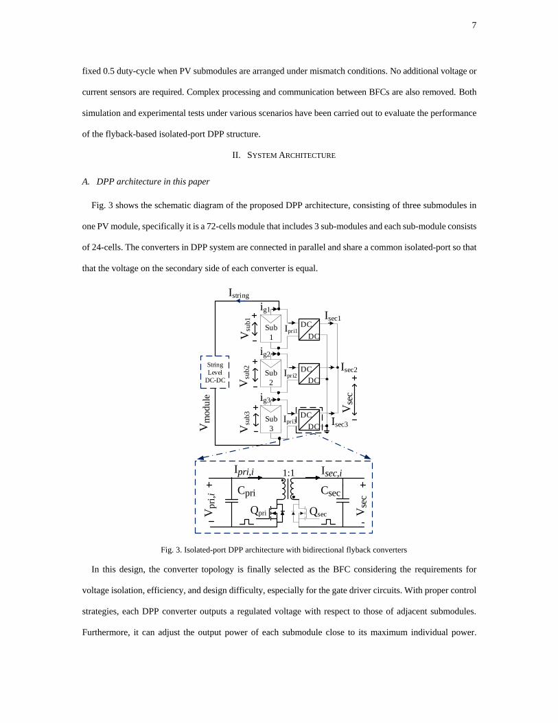
Fig. 3 shows the schematic diagram of the proposed DPP architecture, consisting of three submodules in
one PV module, specifically it is a 72-cells module that includes 3 sub-modules and each sub-module consists
of 24-cells. The converters in DPP system are connected in parallel and share a common isolated-port so that
that the voltage on the secondary side of each converter is equal.
Sub
1Ipri1
Isec1
Isec2
Isec3Vm
od
ule
Vse
c
1:1Ipri,i Isec,i
QpriVp
ri,i
DC
DC
DC
DC
DC
DC
String
Level
DC-DC
Vsu
b1
Vsu
b2
Vsu
b3 V
sec
Qsec
Istring
Sub
2
Sub
3
Cpri Csec
Ipri2
Ipri3
ig1
ig2
ig3
Fig. 3. Isolated-port DPP architecture with bidirectional flyback converters
In this design, the converter topology is finally selected as the BFC considering the requirements for
voltage isolation, efficiency, and design difficulty, especially for the gate driver circuits. With proper control
strategies, each DPP converter outputs a regulated voltage with respect to those of adjacent submodules.
Furthermore, it can adjust the output power of each submodule close to its maximum individual power.

8
Majority current flows directly through the load, and a small fraction of the differential current is processed
by the DPP converter. In this paper, the PV-20 SFP2136 is selected as the PV module, and its main electrical
specifications under the STC are presented in Table I.
TABLE I
PV MODULE SPECIFICATION (PV-20 SFP2136)
Parameter Symbol Value Parameter Symbol Value
Number of cells Ns 24 Maximum power (W) Pmpp 20
Voltage at MPP (V) Vmpp 17.2 Current at MPP (A) Impp 1.11
Open-circuit voltage (V) Voc 21.6 Short-circuit current (A) Isc 1.22
Temperature coeff. Of Voc
(%/oC) NA -0.034
Temperature coeff. Of Isc
(%/oC) NA 0.005
Band energy (eV) Eg 1.12 Ideality factor NA 1.8
Shunt resistance (Ω) Rp 25 Series resistance (Ω) Rs 0.008
B. Control Algorithm
The main objective of the BFCs is to balance the voltage of the submodules, which is called here voltage
equalization. The aim of this control strategy is to keep the voltage in primary and secondary of the DPP
converters same. Specifically, a fixed 50% duty cycle signal is used to control the switches in DPP converter.
The input voltage 𝑉𝑝𝑟𝑖 , output voltage 𝑉𝑠𝑒𝑐 and duty cycle D in flyback converter have the relation as
follows:
sec1
pri
DV V
D
(1)
Furthermore, the secondary sides of the BFCs are connected in parallel. Thus, the output voltage is equal.
Then the equation can be written as follows:
sec _1
sec _ 2
sec _ 3
1
1
1
pri
pri
pri
DV V
D
DV V
D
DV V
D
(2)
where 𝑉𝑝𝑟𝑖_1, 𝑉𝑝𝑟𝑖_2 and 𝑉𝑝𝑟𝑖_3 is the voltage of each substring. Let D is equal to 0.5, then 𝑉𝑠𝑒𝑐 = 𝑉𝑝𝑟𝑖_1 =
𝑉𝑝𝑟𝑖_2 = 𝑉𝑝𝑟𝑖_3. Therefore, the voltage of each substring is controlled to reside on a straight line. Fig. 4
illustrates the operation principle of the submodule flyback converters in DPP architecture to balance the
voltage. To transfer the energy from primary to secondary of BFCs, switch Qpri is controlled by conventional
constant-frequency pulse-width modulation, and the duty cycle is calculated as D=Ton/Ts, where Ton is the

9
switch on time, and Ts is the switching period. Meanwhile, the switch Qsec in the secondary side of BFC is
shut off at all time, and the built-in diode is worked as the flyback diode. If the energy transfer direction is
reversed, the operation of the converters is complete symmetrical: Qpri in primary side is turned off at all time
while its built-in diode acts as the flyback converter, meanwhile, switch Qsec is now controlled by PWM
pulses. Cpri and Csec represent the primary side and secondary side capacitor, respectively.
Transfer power from primary to secondary side
Transfer power from secondary to primary side
VsecQpri QsecCpri Csec
Vsec
Qpri QsecCpri Csec
PWM
PWM Fig. 4. The operation principle of flyback converters in DPP architecture to balance the voltage.
In this paper, voltage equalization, a simple and robust method, is used with no communication or sensing
between primary and secondary of the flyback converter. A complementary signal with frequency 100 kHz
and 0.5 duty ratio are used to control the primary switch Qpri and secondary switch Qsec according to the
power transfer direction. A comparison of the voltage equalization and true MPPT is made in the following
section; it shows that this control method simplifies the system configuration and reduces the cost of hardware.
III. PERFORMANCE EVALUATION
A. Comparison between DPP and bypass diode method
The limitation of the conventional bypass diode method is that the actual output power is significantly
reduced and the output P-V curve shows multi-peaks characteristic under partial shading conditions. Here, a
comparison between the proposed DPP structure and the method of using bypass diodes under different
partial shading scenarios is conducted. Specifically, the following three scenarios are defined: severe
mismatch condition with PV1 fully illuminated, PV2 half illuminated, and PV3 25% illuminated; moderate
mismatch condition with the normalized illumination values for these three submodules 100%, 75%, and
50%; slight mismatch condition, the normalized illumination values for these submodules are 100%, 90%,

10
and 80%. As illustrated in Fig. 5(a) and (b), under the slight mismatch condition, the reduction of output
power produced by the bypass diode method is not distinct, and the improvement with the proposed DPP is
small, specifically 5.32%. It shows that PV module will operate at near the theoretical maximum power
output point and the power proceeded by the BFCs is very small. However, with the increase of partial
shading area, the improvement with the DPP becomes larger, specifically 33.91% for moderate partial
shading condition and 56.25% for serious partial shading condition. Under these two scenarios, the module
current Imodule mainly limited by the weakest submodule and a large portion of the power produced by the
strongest submodule cannot be used without DPP converters.
(a) (b)
(c) (d)
(e) (f)
Fig. 5. Simulation results comparison: (a) P-I curve for slight mismatch condition (PV1: 100%, PV2: 90%, PV3: 80%);
(b) V-I curve for slight mismatch condition (PV1: 100%, PV2: 90%, PV3: 80%); (c) P-I curve for moderate mismatch
condition (PV1: 100%, PV2: 75%, PV3: 50%); (d) V-I curve for moderate mismatch condition (PV1: 100%, PV2: 75%,
PV3: 50%); (e) P-I curve for severe mismatch condition (PV1: 100%, PV2: 50%, PV3: 25%); (f) V-I curve for severe
mismatch condition (PV1: 100%, PV2: 50%, PV3: 25%).
Fig. 6 illustrates the difference of maximum output power between DPP and the bypass diode method in
all irradiance conditions. In this test, the normalized insolation of the submodule 1 is always set to 100%.

11
The normalized insolation of sub-module 2 is set to 25%, 50%, 75% and 100%, and the normalized insolation
of sub-module 3 is swept from 10%to 100%. Fig. 6 shows that the output power improvement is high up to
86% for the mismatch condition of PV1:100%, PV2: 25%, and PV3: 40%. As can be seen, a significant
output power improvement can be achieved using DPP architecture, especially when the partial shading
becomes more severe. In the moderate or severe partial shading scenarios, the string current is limited by the
weakest submodules so that a significant portion of energy cannot be output for the system without DPP
technology. The improvement of the maximum production power is not apparent when the mismatch among
each submodule is slight. In these scenarios, each submodule typically works near the theoretical maximum
output power, most of the energy flows directly into the string level control converters since the DPP
converters only need to process very little power.
Fig. 6. Output power improvement under various insolation conditions
B. Comparison between True MPPT and voltage Equalization
Voltage equalization is used here since it doesn’t require additional voltage or current sensors. Furthermore,
the complex processing and communication between BFCs can also be removed. Thus, it’s well suited for
low-cost integrated hardware scheme. The basic principle of voltage equalization is to keep the voltage of
each substring at the same straight line. However, it cannot ensure the operation point is the exact maximum
power point because the MPP voltage for one PV panel is always changing with the temperature and
irradiance as shown in Fig. 7. Nevertheless, when the mismatch between each submodule is not severe, the
MPP voltage of each substring is nearly same.

12
(a) (b)
Fig. 7. (a) Solar P-V and I-V curve with variation in temperature at constant irradiance (1KW/m2), (b) solar P-V and I-V
curve with variation in irradiance at constant temperature (25oC).
The following simulation has been tested in Matlab/Simulink to quantify the difference between true
MPPT and voltage equalization, and the model is presented Fig. 8. A fixed-step P&O MPPT algorithm is
used in this test. PV 1 is fixed at 100% normalized irradiance, PV 2 is fixed at 50% normalized irradiance
and PV 3 is fixed at 25% normalized irradiance. The specifications of these three insolation conditions for
PV-20 SFP2136 are listed in Table. II. The load used in this test is 40Ω. The output power and voltage of
each PV panel for true MPPT and voltage equalization are observed.
TABLE. II
SPECIFICATION OF PV-20 SFP2136 WITH DIFFERENT IRRADIANCE
Fig. 8. Simulation model of the DPP module.
Irradiance MPP Voltage MPP Current Maximum Power
1000W/m2 18 V 1.11 A 19.98 W
500W/m2 17.8 V 0.556 A 9.9 W
250W/m2 17.41 V 0.278 A 4.845 W

13
(a) (b)
Fig. 9. Voltage waveform, power waveform and duty cycle of each substring by using true MPPT control method: (a)
output voltage; (b) output power.
(a) (b)
Fig. 10. Simulation results of each substring by using the voltage equalization method: (a) voltage waveform, (b) power
waveform.
Fig. 9 presents the voltage waveform, power waveform and duty cycle of each substring by using true
MPPT control. Fig. 10 presents the voltage waveform and power waveform by using method presented in
this paper. The total output power with the true MPPT method is 34.73W, while the total output power of the
voltage equalization method is 34.639 W with high efficiency of 99.73 %. The results can be summarized in
14
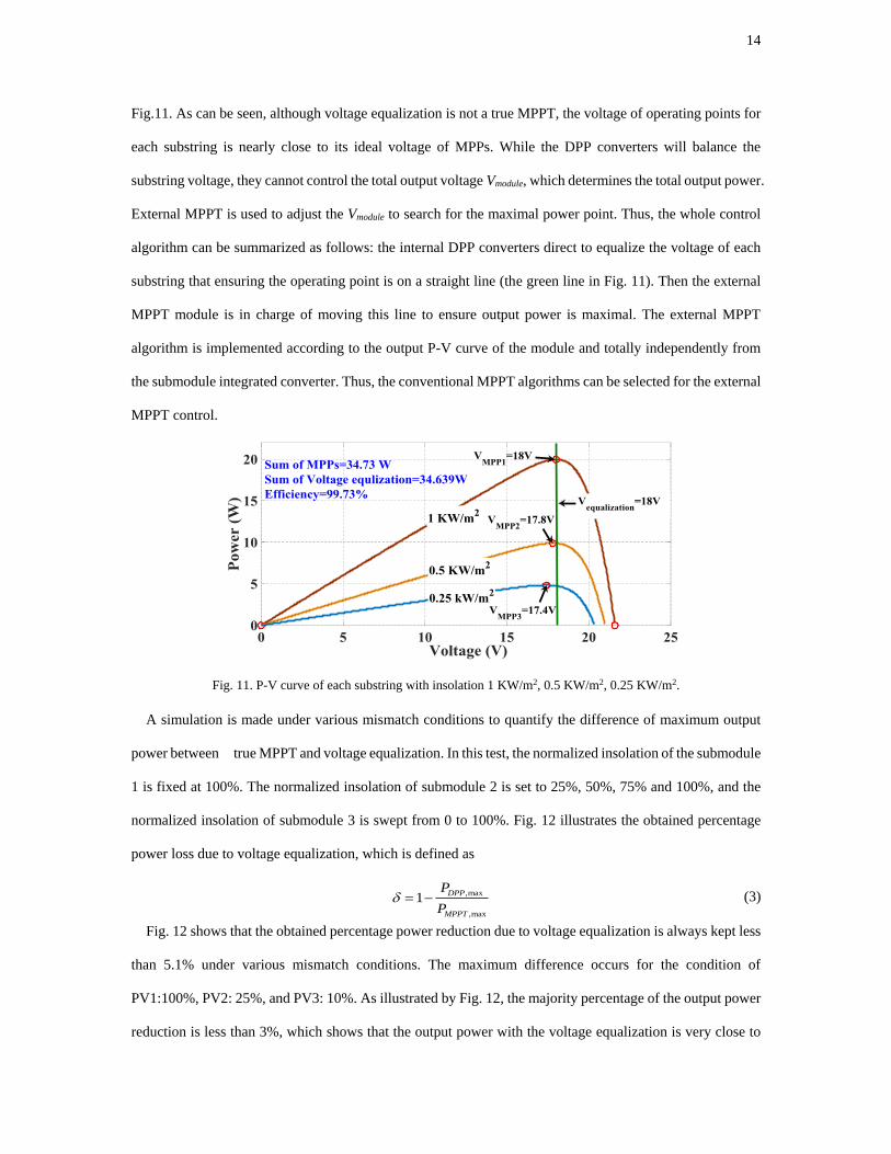
Fig.11. As can be seen, although voltage equalization is not a true MPPT, the voltage of operating points for
each substring is nearly close to its ideal voltage of MPPs. While the DPP converters will balance the
substring voltage, they cannot control the total output voltage Vmodule, which determines the total output power.
External MPPT is used to adjust the Vmodule to search for the maximal power point. Thus, the whole control
algorithm can be summarized as follows: the internal DPP converters direct to equalize the voltage of each
substring that ensuring the operating point is on a straight line (the green line in Fig. 11). Then the external
MPPT module is in charge of moving this line to ensure output power is maximal. The external MPPT
algorithm is implemented according to the output P-V curve of the module and totally independently from
the submodule integrated converter. Thus, the conventional MPPT algorithms can be selected for the external
MPPT control.
Fig. 11. P-V curve of each substring with insolation 1 KW/m2, 0.5 KW/m2, 0.25 KW/m2.
A simulation is made under various mismatch conditions to quantify the difference of maximum output
power between true MPPT and voltage equalization. In this test, the normalized insolation of the submodule
1 is fixed at 100%. The normalized insolation of submodule 2 is set to 25%, 50%, 75% and 100%, and the
normalized insolation of submodule 3 is swept from 0 to 100%. Fig. 12 illustrates the obtained percentage
power loss due to voltage equalization, which is defined as
,max
,max
1DPP
MPPT
P
P (3)
Fig. 12 shows that the obtained percentage power reduction due to voltage equalization is always kept less
than 5.1% under various mismatch conditions. The maximum difference occurs for the condition of
PV1:100%, PV2: 25%, and PV3: 10%. As illustrated by Fig. 12, the majority percentage of the output power
reduction is less than 3%, which shows that the output power with the voltage equalization is very close to

15
the ideal maximum output power by using the complicated MPPT control for each submodule integrated
converter. However, voltage equalization significantly reduces the control complexity since it can operate
with open-loop control simply without real-time communication. Compared with true MPPT algorithm, the
module current Imodule doesn’t be measured, which reduces the system cost. Furthermore, the proposed DPP
can achieve satisfactory tracking efficiency. Consider the fact; the severe mismatch doesn’t frequently occur
in real-world installations. Thus, the voltage equalization is a satisfactory solution for the practical application.
Fig. 12. Percentage power loss due to voltage equalization
C. Transient
Fig. 13 shows simulation results of the primary currents of each sub-module under dynamics. The electronic
load of the whole system is 40Ω. In this simulation, all submodules are supplied with a same current 1.22A
(meaning they have the same insolation level without any mismatch) at t=0. Then, at t=0.4s, the supplied
current of submodule 2 becomes to 0.47A to emulate the mismatch condition. The primary theoretical current
of DPP converters can be calculated by using following equation:
1 2 3
1 1
1 2 3
2 2
1 2 3
3 3
3
3
3
g g g
pri g
g g g
pri g
g g g
pri g
i i ii i
i i ii i
i i ii i
(4)
It should be noted that the sum of the primary current of all BFCs is zero that can be written as 𝐼𝑝𝑟𝑖1 +
𝐼𝑝𝑟𝑖2 + 𝐼𝑝𝑟𝑖3 = 0. Thus, the submodule 1 and submodule 3 eject currents and the mismatched submodule 2
extracts the current from others submodules.

16
Fig. 13. The simulated current of each submodule during the mismatch transient.
The detailed dynamic waveforms during the time from 0.4s to 0.6s are illustrated in Fig. 14. The current
of Ipri1 and Ipri3 are 0.25A and Ipri2 is -0.5A under the mismatch condition. At t=0.6s, the current of submodule
2 recovers to 1.22A and the BFCs stop extracting and ejecting currents. All primary currents of BFCs return
to zero. The process can be illustrated specifically in Fig. 15.
Fig. 14. Detailed primary current transient in each submodule.
Ipri1=0.25A Isec1=0.25A
Vse
c
1:1
Qpri QsecCpri Csec
Ipri2=0.5A Isec2=0.5A
Vse
c
1:1
Qpri QsecCpri Csec
Ipri3=0.25A Isec3=0.25A
Vse
c
1:1
Qpri QsecCpri Csec
1.2
2A
0.4
7 A
1.2
2A
ig1
ig2
ig3
LO
AD
Fig. 15. The current following of each submodule flyback converter under partial shading.
IV. EXPERIMENTAL RESULTS
A. Experimental Setup

17
The system diagram of the experimental test setup and the detailed test bench arrangement are illustrated
in Fig. 16 and Fig. 17, respectively. In the test, a 72-cells module was used, which can be separated into 3
sub-modules and each sub-module consists of 24 cells. In the test, considering the convenience in wire
connecting, each sub-module was implemented by a 24-cells module. In this configuration, current source
Iphi (i=1, 2, 3) is used to emulate the partial shading in three sub-modules. Practically the photo-diode Iph for
each sub-module is implemented by a DC power supply connected in parallel with each submodule and
operated in current-limited mode. Different level of insolation can be easily accomplished by changing the
value of Iph. Thus, thus different partial shading conditions can be emulated. This indoor test was adopted
considering its advantage of easy implementation and the repeatability.
Sub-Module 1
SubMIC 1
FLYBACK
Converter
Sub-Module 2
SubMIC 2
FLYBACK
Converter
Sub-Module 3
SubMIC 3
FLYBACK
Converter
Isola
ted
-po
rt
Vse
c
Electronic
Load
Iph
Iph
Id Ip I Cpv
Id Ip I Cpv
CpvIIpId
Istring
I ph
1I p
h2
I ph3
Iph
Fig. 16. Experimental test setup
The detailed test bench arrangement of the experiment is illustrated in Fig. 17. A prototype system has
been built around PV-20 SFP2136 PV module with three BFCs attached three 24-cell substrings. Bias current
source using in this paper is LK3303D connecting parallel with each submodule to emulate varying
irradiation levels. DSP model TMS320F28335 is utilized in this experiment connecting with the computer to
generate three sets of complementary signals input to the MOSFETs IRF740 in BFCs. Signal channel DC
electronic load IT8514C+ used here to emulated external MPPT to control output module voltage 𝑉𝑚𝑜𝑑𝑢𝑙𝑒.
Voltage probe DP6130A and connecting with the voltage and current probes to read the waveforms.

18
1
2
3 4
56
7
9
Fig. 17. Experimental test bench (1: PV sub-modules, 2: Computer, 3: DSP module, 4: Flyback converters, 5: Driving
power supply, 6: Oscilloscope, 7: Bias Current Source, 8: Electronic Load, 9: Voltage and current probes)
Since the bidirectional flyback converters (BFCs) used in the DPP architecture process only the mismatch
power of the PV submodules, which leads to reduced size, weight, and cost of the BFCs. Furthermore, the
voltage rating of switching devices is reduced, which is same as the output voltage of each sub-module.
Besides, the BFCs are only activated when partial shading is detected, which is also beneficial to the power
loss reduction.
Two possible failure cases are considered: one case is that the primary or secondary port of one BFC
operated under the open-circuit condition, the other case is the short-circuit condition in the secondary port
of one submodule. For the former case, the actual output power is less power than that of MPP. However,
due to the inside bypass diode of this submodule, the submodule still operates normally, and the output power
reduction is relieved to some extent under mismatch conditions. For the latter case, it is usually regarded as
the worth case, and thus all BFCs must be disabled to protect the entire system.
B. Bidirectional Flyback Converter Design and Test
To evaluate the effectiveness of the BFC based DPP architecture for PV system application, a real BFC
prototype was designed and illustrated in Fig. 18.
SubMIC_1SubMIC_2SubMIC_3
Fig. 18. Hardware prototype of the bidirectional flyback converter

19
When one 20W sub-module is fully illuminated, and the other two are completely shaded, the mismatch
power is estimated around 13.3W. Thus, the power rating of the BFC was set as 15W. The switching device
was selected as IRF740 and the switching frequency is 100 kHz. The transformer was designed with 10 turns
of 18# Litz wire on the primary and secondary. The transformer was designed with 10 turns of 18# Litz wire
on the primary and secondary. Litz wire is widely used in high-frequency transformer design since it can
reduce the skin effect and proximity effect losses in conductors for high frequency applications. The magnetic
inductance was 50μH and the leakage inductance was designed nearly 230nH. A snubber circuit with a
diode and a 47pf capacitor was used to protect the main device MOSFET. The specific values of BFC are
shown in Table III.
TABLE III
FLYBACK CONVERTER SPECIFICATION
An experimental test of the conversion efficiencies for the BFC was conducted and Fig. 19 shows key
waveforms of the BFC with a constant duty cycle of 0.5 under different operating conditions. Fig. 19(a)
illustrates the key waveforms of BFC under the slight partial shading condition, which indicates that the
converter is working in discontinuous conduction mode (DCM). Fig. 19 (b) illustrates the key waveforms of
BFC under the severe partial shading condition, which indicates that the converter is working in continuous
conduction mode (CCM). Thus, different operation modes are used to improve the efficiency. Fig. 20 shows
the measured efficiency of the BFC with respect to the output power, which indicates that the design BFC
can achieve efficiency higher than 90% of a wide range of output power.
Parameter Value
Input voltage 4-21V
Flyback converter switching frequency 100kHz
Primary and secondary flyback converter switch IRF740
Flyback converter turn ratio 1:1
Magnetizing inductance 50μH
Power Rating 15W
Primary and secondary capacitor 2200μH

20
(a) (b) Fig. 19. Experimental waveforms of BFCs for two operating conditions: (a) slight partial shading condition; (b) severe
partial shading condition.
Fig. 20. Experimental efficiency for the bidirectional flyback converter with respect to the output power
C. Indoor Test
The experimental test setup is illustrated in Fig. 16. Main experimental setup was described in the section
A. An electronic load, IT5814C+, is used as a central converter. Five multimeters are used to measure the
voltage of each submodule; besides, the module-level voltage and current are also measured. In the indoor
test, the short-circuit currents of the three sub-modules are tuned from 0A to 1.22A to emulate different
partial shading conditions. To evaluate the performance of this BFC based DPP architecture, both the P-I and
V-I curves with and without DPP algorithm are measured. As illustrated by Fig. 17, the electronic load is
connected with the submodules and swept from 10Ω to 200Ω within 60 steps to perform a dc voltage sweep
in order to characterize the P-I and V-I curves of the PV module. Fig. 21 illustrates main experimental results
under three partial shading conditions. The definitions for three scenarios are the same as the simulation.
Table IV also lists the comparison results of output power under different scenarios. As illustrated in Fig. 21
(a) and (b), under the slight mismatch condition, the P-I curves and V-I curves obtained from simulation and
experiments are also overlapped since the BFCs only process a very small portion power. Under this scenario,
as illustrated in Table IV, the improvement with the DPP structure through simulation and experiments is
5.32% and 3%, respectively. Considering the practical power loss of BFCs, the measured power improvement
by experiment is lower than that of simulation. As illustrated in Fig. 21 (c) and (d), under the moderate
mismatch condition, the difference of P-I curves and V-I curves obtained from simulation and experiments
becomes larger. Under this scenario, the improvement with the DPP structure through simulation and
experiments is 33.91% and 26%, respectively. Under the severe mismatch conditions, as illustrated in Table
IV, the improvement with the DPP structure through simulation and experiments is 56.25% and 43.13%,

21
respectively. Consider the power loss in DPP converters during the test, the maximum power measured in
the experiment is less than simulation. Furthermore, this error becomes more apparent when the mismatch
level become severe because of more power loss in DPP converters in the experiment.
TABLE IV
EXPERIMENTAL RESULTS OF OUTPUT POWER UNDER DIFFERENT SCENARIOS
Mismatch Level Slight Moderate Severe
Maximum power with DPP (SIM Results) 53.61 W 44.14 W 32.95 W
Maximum power with DPP (EXP Results) 52.29 W 41.5 W 30.23 W
Maximum power with Bypass Diodes 50.9 W 32.96 W 21.12 W
Improvement with DPP in SIM 5.32% 33.91% 56.25%
Improvement with DPP in EXP 3% 26% 43.13%
(a) (b)
(c) (d)
(e) (f)
Fig. 21. Experimental results comparison: (a) P-I curve for slight mismatch condition (PV1: 100%, PV2: 90%, PV3:
80%); (b) V-I curve for slight mismatch condition (PV1: 100%, PV2: 90%, PV3: 80%); (c) P-I curve for moderate
mismatch condition (PV1: 100%, PV2: 75%, PV3: 50%); (d) V-I curve for moderate mismatch condition (PV1: 100%,
PV2: 75%, PV3: 50%); (e) P-I curve for severe mismatch condition (PV1: 100%, PV2: 50%, PV3: 25%); (f) V-I curve
for severe mismatch condition (PV1: 100%, PV2: 50%, PV3: 25%).

22
The overall efficiency of the DPP system is measured under two operating conditions: no shading
condition (bias current is 1.22A, 1.22A and 1.22A) and severe shading condition (bias current is 1.22A,
0.61A and 0.31A). The measured results under two conditions are illustrated in Table V, which indicates that
an efficiency of 99.8% can be achieved without partial shading. Under this condition, all BFCs are bypassed
and no power loss produced. With severe shading, the overall efficiency is 90% due to more mismatch power
is processed by BFCs. Thus, additional power losses will be produced, and the system efficiency is affected.
However, more output power is achieved by using the DPP structure, as illustrated in Table V.
TABLE V
MEASURED EFFICIENCY RESULTS UNDER TWO OPERATION CONDITIONS
Condition No Shading Severe Shading
Bias Current of each Substring 1.22 A 1.22A 1.22A 1.22A 0.61A 0.31A
Sum of MPPs (ideal output power) 60 W 33.5 W
Measure Maximum String Power 59.1 W 30.23 W
Power loss in BFCs 0.9 W 3.27 W
Efficiency 98.50% 90.23%
D. Transient Test
Transient performance is evaluated since totally three BFCs are used in the DPP structure. Similar to the
transient simulation setting in Fig. 14, initially all submodules are supplied with the same current 1.22A.
Then, at t=1.5s, the injected current to submodule 1 is reducing to 0.47A to emulate the partial shading. The
measured current is: 𝑖𝑝𝑟𝑖1 = −0.5𝐴, 𝐼𝑝𝑟𝑖2 = 𝐼𝑝𝑟𝑖3 = 0.25𝐴 as illustrated in Fig. 22, which verifies the above
theoretical steady-state analysis. The current redistribution dynamics among three branches are almost
finished during the same period. The transient time is measured as 0.26s, which is higher than the simulation
result of 0.06s considering the effect of parasitic effect, and single time delay. At t=3.75s, partial shading is
setting disappeared, and the current for submodule 1 is increased to the normal bias current 1.22A. Fig. 22
shows that and the currents following through the BFCs are reduced to 0A. The current redistribution
dynamics among three branches also shows good consistency.

23
-0.5A
0.25A
0.25A
Time 0.6s/div
Ch2: Ipri 1
Ch3: Ipri 2
Ch4: Ipri 3
0.5A/div
0.5A/div
0.5A/div
Fig. 22. Experimental transient response.
V. CONCLUSION
In this paper, we addressed the problem of submodule mismatch in partially-shaded PV modules by using
bidirectional flyback-based isolated-port differential power-processing optimizers. Different to the PV-to-
PV and PV-to-bus structure, the PV-to-isolated port structure is adopted since it processes the least power
and shows potentially highest efficiency among different DPP structures. Furthermore, with this DPP
structure, the voltage conversion ratio of the submodule DC-DC converters is close to unity, allowing low
voltage components. The bidirectional flyback topology was selected since it can achieve voltage isolation,
high efficiency for a wide range, and easy gate driver circuit design. The flyback converter designed to work
in discontinuous conduction mode (DCM) for the slight mismatch condition and continuous conduction mode
(CMM) for the severe mismatch condition to minimize the power loss. The voltage equalization with open-
loop control is used to regulate the submodule flyback converter. The duty-ratio of submodule flyback
converter is set as a fixed number with 0.5, and the frequency is 100 kHz. It’s simple, easy-to-implement and
well suited for low-cost integrated hardware scheme since it does not require additional voltage or current
sensors. Besides, complex processing and communication between BFCs are removed. Both simulation and
experimental results for a 72-cells PV module are provided. The measured efficiency with the isolated-port
DPP structure was 98.50% with no shading, and 90.23% under severe shading condition. Under the moderate
shading condition, the measured output power improvement was 26%. Under severe mismatch condition, the
corresponding improvement was high up to 43.1%.

24
ACKNOWLEDGEMENTS
This research was supported by the University Research Development Fund (RDF-14-02-03), the State
Key Laboratory of Power Transmission Equipment & System Security and New Technology
(2007DA10512716414), the Jiangsu Science and Technology Programme (BK20161252), and the National
Nature Science Foundation of China (51407145).
REFERENCE
Bai, J., Y. Cao, Y. Hao, Z. Zhang, S. Liu and F. Cao., 2015. Characteristic output of PV systems under partial
shading or mismatch conditions. Solar Energy 112: 41-54.
Bell, R. and R. C. N. Pilawa-Podgurski., 2015. Decoupled and Distributed Maximum Power Point Tracking
of Series-Connected Photovoltaic Submodules Using Differential Power Processing. IEEE Journal of
Emerging and Selected Topics in Power Electronics 3(4): 881-891.
Ben-Yaakov, S., A. Blumenfeld, A. Cervera and M. Evzelman., 2012. Design and evaluation of a modular
resonant switched capacitors equalizer for PV panels. 2012 IEEE Energy Conversion Congress and
Exposition (ECCE).
Daliento, S., F. Di Napoli, P. Guerriero and V. d’Alessandro., 2016. A modified bypass circuit for improved
hot spot reliability of solar panels subject to partial shading. Solar Energy 134(Supplement C): 211-218.
Du, Y. and D. D.-C. Lu., 2011. Battery-integrated boost converter utilizing distributed MPPT configuration
for photovoltaic systems. Solar Energy 85(9): 1992-2002.
Eng, V. and C. Bunlaksananusorn., 2009. Modeling of a SEPIC converter operating in Discontinuous
Conduction Mode. 2009 6th International Conference on Electrical Engineering/Electronics, Computer,
Telecommunications and Information Technology.
Eng, V., U. Pinsopon and C. Bunlaksananusorn., 2009. Modeling of a SEPIC converter operating in
Continuous Conduction Mode. 2009 6th International Conference on Electrical Engineering/Electronics,
Computer, Telecommunications and Information Technology.
Khan, O. and W. Xiao., 2016. An Efficient Modeling Technique to Simulate and Control Submodule-
Integrated PV System for Single-Phase Grid Connection. IEEE Transactions on Sustainable Energy 7(1):
96-107.
Khan, O. and W. Xiao., 2017. Review and qualitative analysis of submodule-level distributed power
electronic solutions in PV power systems. Renewable and Sustainable Energy Reviews 76: 516-528.
Kim, K. A., G. S. Seo, B. H. Cho and P. T. Krein., 2016. Photovoltaic Hot-Spot Detection for Solar Panel
Substrings Using AC Parameter Characterization. IEEE Transactions on Power Electronics 31(2): 1121-
1130.
Kim, K. A., P. S. Shenoy and P. T. Krein., 2015. Converter Rating Analysis for Photovoltaic Differential
Power Processing Systems. IEEE Transactions on Power Electronics 30(4): 1987-1997.

25
Lappalainen, K. and S. Valkealahti., 2017. Effects of PV array layout, electrical configuration and geographic
orientation on mismatch losses caused by moving clouds. Solar Energy 144(Supplement C): 548-555.
Levron, Y., D. R. Clement, B. Choi, C. Olalla and D. Maksimovic., 2014. Control of Submodule Integrated
Converters in the Isolated-Port Differential Power-Processing Photovoltaic Architecture. IEEE Journal
of Emerging and Selected Topics in Power Electronics 2(4): 821-832.
Li, X., H. Wen, L. Jiang, Y. Hu and C. Zhao., 2016. An Improved Beta Method With Autoscaling Factor for
Photovoltaic System. IEEE Transactions on Industry Applications 52(5): 4281-4291.
Mäki, A. and S. Valkealahti., 2012. Power Losses in Long String and Parallel-Connected Short Strings of
Series-Connected Silicon-Based Photovoltaic Modules Due to Partial Shading Conditions. IEEE
Transactions on Energy Conversion 27(1): 173-183.
Mai, T. D., S. De Breucker, K. Baert and J. Driesen., 2017. Reconfigurable emulator for photovoltaic modules
under static partial shading conditions. Solar Energy 141: 256-265.
Olalla, C., D. Clement, M. Rodriguez and D. Maksimovic., 2013. Architectures and Control of Submodule
Integrated DC-DC Converters for Photovoltaic Applications. IEEE Transactions on Power Electronics
28(6): 2980-2997.
Qin, S., C. B. Barth and R. C. N. Pilawa-Podgurski., 2016. Enhancing Microinverter Energy Capture With
Submodule Differential Power Processing. IEEE Transactions on Power Electronics 31(5): 3575-3585.
Qin, S., S. T. Cady, A. D. Domínguez-García and R. C. N. Pilawa-Podgurski., 2015. A Distributed Approach
to Maximum Power Point Tracking for Photovoltaic Submodule Differential Power Processing. IEEE
Transactions on Power Electronics 30(4): 2024-2040.
Radjai, T., L. Rahmani, S. Mekhilef and J. P. Gaubert., 2014. Implementation of a modified incremental
conductance MPPT algorithm with direct control based on a fuzzy duty cycle change estimator using
dSPACE. Solar Energy 110: 325-337.
Rezk, H. and A. M. Eltamaly., 2015. A comprehensive comparison of different MPPT techniques for
photovoltaic systems. Solar Energy 112: 1-11.
Schaef, C., K. Kesarwani and J. T. Stauth., 2013. A coupled-inductor multi-level ladder converter for sub-
module PV power management. 2013 Twenty-Eighth Annual IEEE Applied Power Electronics
Conference and Exposition (APEC).
Shenoy, P. S., K. A. Kim, B. B. Johnson and P. T. Krein., 2013. Differential Power Processing for Increased
Energy Production and Reliability of Photovoltaic Systems. IEEE Transactions on Power Electronics
28(6): 2968-2979.
Solórzano, J. and M. A. Egido., 2014. Hot-spot mitigation in PV arrays with distributed MPPT (DMPPT).
Solar Energy 101: 131-137.
Tey, K. S. and S. Mekhilef., 2014. Modified incremental conductance MPPT algorithm to mitigate inaccurate
responses under fast-changing solar irradiation level. Solar Energy 101: 333-342.

26
Uno, M. and A. Kukita., 2015. Current sensorless single-switch voltage equalizer using multi-stacked buck-
boost converters for photovoltaic modules under partial shading. 2015 9th International Conference on
Power Electronics and ECCE Asia (ICPE-ECCE Asia).
Villa, L. F. L., T. P. Ho, J. C. Crebier and B. Raison., 2013. A Power Electronics Equalizer Application for
Partially Shaded Photovoltaic Modules. IEEE Transactions on Industrial Electronics 60(3): 1179-1190.
Zhou, H., J. Zhao and Y. Han., 2015. PV Balancers: Concept, Architectures, and Realization. IEEE
Transactions on Power Electronics 30(7): 3479-3487.


![Catalogue FLYBACK Equivalent - [PDF Document] FLYBACK Equivalent FlyBack Equivalent flyback reemplazo conversor Flyback tv fly-back Flyback Tester Flyback Converter conversor Flyback](https://img.dokumen.tips/doc/110x75/5a832a447f8b9a9d308e9416/catalogue-flyback-equivalent-pdf-document-flyback-equivalent-flyback-equivalent.jpg)