Embed Size (px)
Citation preview

EECS 247 Lecture 8: SC Filters © 2004 H. K. Page 1A/DDSP
EE247Lecture 8
• Finishing Continuous-time filters– Various Gm-C Filter implementations– Comparison of continuous-time filter topologies
• Switched-Capacitor Filters– “Analog” sampled-data filters:
• Continuous amplitude• Quantized time
– Applications:• First commercial product: Intel 2912 voice-band CODEC chip,
1979• Oversampled A/D and D/A converters• Stand-alone filters
E.g. National Semiconductor LMF100
EECS 247 Lecture 8: SC Filters © 2004 H. K. Page 2A/DDSP
BiCMOS Gm-Cell• MOSFET in triode mode:
• Note that if Vds is kept constant:
• Linearity performance function of how constant Vds can be held
– Gain @ Node X must be minimized
• Since for a given current, gm of BJT is larger compared to MOS preferable to have BJT
• Extra pole at node X
( )C Wox 2V VI 2 V Vgs thd ds ds2 L
I Wd Cg Vm ox dsV Lgs
M1 B1A g gx m m
µ
µ
−= −
∂= =
∂
=
B1
M1X
Iout
Is
Vgs+Vin
Vb
gm can be varied by changing Vb and thus Vds

EECS 247 Lecture 8: SC Filters © 2004 H. K. Page 3A/DDSP
• Differential- needs common-mode feedback ckt
• Freq. tuned by varying Vb
• Design tradeoffs:– Extra poles at the input device
drain junctions– Input devices have to be small
to minimize parasitic poles– Results in high input-referred
offset voltage à could drive ckt into non-linear region
– Small devices à high 1/f noise
BiCMOS Gm-C Integrator
-Vout
+
Cintg/2
Cintg/2
EECS 247 Lecture 8: SC Filters © 2004 H. K. Page 4A/DDSP
7th Order Elliptic Gm-C LPFFor CDMA RX Baseband Application
+A- +B-+ -
+A- +B-+ -
+A- +B-+ -
+A- +B-+ -
+A- +B-
+-
+A- +B-
+-
+A- +B-
+-
Vout
Vin
+C-
• Gm-Cell in previous page used to build a 7th order elliptic filter for CDMA baseband applications (650kHz corner frequency)
• In-band dynamic range of <50dB achieved

EECS 247 Lecture 8: SC Filters © 2004 H. K. Page 5A/DDSP
• Used to build filter for disk-drive applications
• Since high frequency of operation, time-constant sensitivity to parasitic caps significant.à Opamp used
• M2 & M3 added to compensate for phase lag (provides phase lead)
Ref: C. Laber and P.Gray, “A 20MHz 6th Order BiCMOS Parasitic Insensitive Continuous-time Filter &Second Order Equalizer Optimized for Disk Drive Read Channels,” IEEE Journal of Solid State Circuits, Vol. 28, pp. 462-470, April 1993.
BiCMOS Gm-OTA-C Integrator
EECS 247 Lecture 8: SC Filters © 2004 H. K. Page 6A/DDSP
6th Order BiCMOS Continuous-time Filter &
Second Order Equalizer for Disk Drive Read Channels
• Gm-C-opamp of the previous page used to build a 6th order filter for Disk Drive
• Filter consists of 3 biquads with max. Q of 2 each• Performance in the order of 40dB SNDR achieved for
variable corner frequency in discrete steps up to 20MHzRef: C. Laber and P.Gray, “A 20MHz 6th Order BiCMOS Parasitic Insensitive Continuous-time Filter &
Second Order Equalizer Optimized for Disk Drive Read Channels,” IEEE Journal of Solid State Circuits, Vol. 28, pp. 462-470, April 1993.

EECS 247 Lecture 8: SC Filters © 2004 H. K. Page 7A/DDSP
Gm-CellSource-Coupled Pair with Degeneration
Ref: I.Mehr and D.R.Welland, "A CMOS Continuous-Time Gm-C Filter for PRML Read Channel Applications at 150 Mb/s and Beyond", IEEE Journal of Solid-State Circuits, April 1997, Vol.32, No.4, pp. 499-513.
– Gm-cell intended for low Q disk drive filter
EECS 247 Lecture 8: SC Filters © 2004 H. K. Page 8A/DDSP
Gm-CellSource-Coupled Pair with Degeneration
– M7,8 operating in triode mode determine the gm of the cell– Feedback provided by M5,6 maintains the gate-source voltage of M1,2
constant by forcing their current to be constantà helps linearize rds of M7,8
– Current mirrored to the output via M9,10 with a factor of k– Performance level of about 50dB SNDR at fcorner of 25MHz achieved

EECS 247 Lecture 8: SC Filters © 2004 H. K. Page 9A/DDSP
• Needs higher supply voltage compared to the previous design
• M5 & M6 configured as capacitors added to compensate for RHP zero due to Cgd of M1 & M2 (moves it to LHP) size of M5-6 is 1/3 of M1-2
• Current ID used to tune filter critical frequency
• M3, M4 operate in triode mode and added to provide CMFB
Ref: R. Alini, A. Baschirotto, and R. Castello, “Tunable BiCMOS Continuous-Time Filter for High-Frequency Applications,” IEEE Journal of Solid State Circuits, Vol. 27, No. 12, pp. 1905-1915, Dec. 1992.
BiCMOS Gm-C Integrator
EECS 247 Lecture 8: SC Filters © 2004 H. K. Page 10A/DDSP
BiCMOS Gm-C Filter For Disk-Drive Application
Ref: R. Alini, A. Baschirotto, and R. Castello, “Tunable BiCMOS Continuous-Time Filter for High-Frequency Applications,” IEEE Journal of Solid State Circuits, Vol. 27, No. 12, pp. 1905-1915, Dec. 1992.
• Using the integrators shown in the previous page• Biquad filter for disk drives• gm1=gm2=gm4=2gm3• Q=2• Tunable from 8MHz to 32MHz
EECS 247 Lecture 8: SC Filters © 2004 H. K. Page 11A/DDSP
Summary Continuous-Time Filters
• Opamp RC filters– Good linearity à High dynamic range (60-90dB)– Only discrete tuning possible– Medium usable signal bandwidth (<10MHz)
• Opamp MOSFET-C– Linearity compromised (typical dynamic range 40-60dB)– Continuous tuning possible– Low usable signal bandwidth (<5MHz)
• Opamp MOSFET-RC– Improved linearity compared to Opamp MOSFET-C (D.R. 50-90dB)– Continuous tuning possible– Low usable signal bandwidth (<5MHz)
• Gm-C – Highest frequency performance (at least an order of magnitude higher
compared to the rest <100MHz)– Dynamic range not as high as Opamp RC but better than Opamp
MOSFET-C (40-70dB)
EECS 247 Lecture 8: SC Filters © 2004 H. K. Page 12A/DDSP
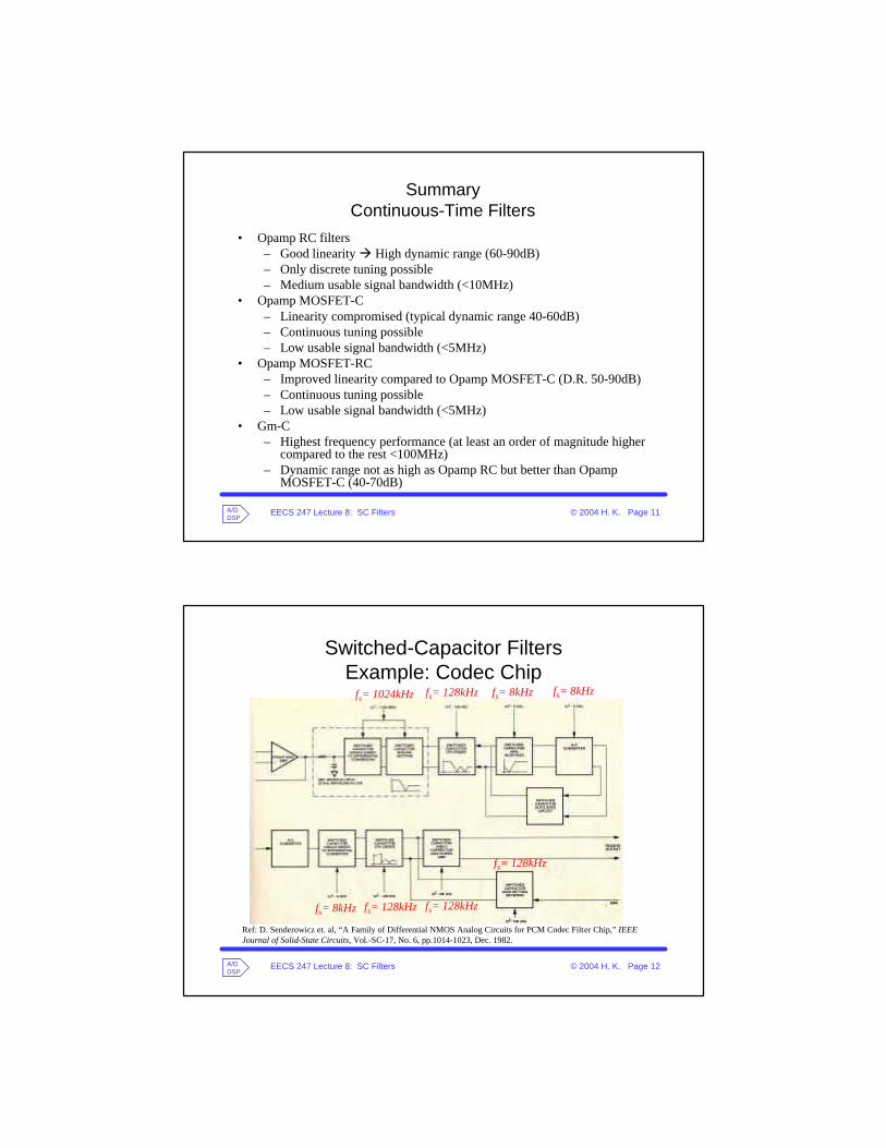
Switched-Capacitor FiltersExample: Codec Chip
Ref: D. Senderowicz et. al, “A Family of Differential NMOS Analog Circuits for PCM Codec Filter Chip,” IEEE Journal of Solid-State Circuits, Vol.-SC-17, No. 6, pp.1014-1023, Dec. 1982.
fs= 1024kHz fs= 128kHz fs= 8kHz fs= 8kHz
fs= 8kHz fs= 128kHz fs= 128kHz
fs= 128kHz
EECS 247 Lecture 8: SC Filters © 2004 H. K. Page 13A/DDSP
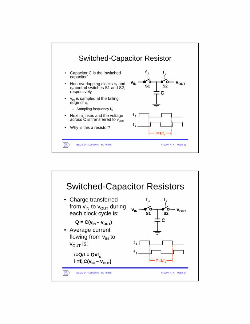
Switched-Capacitor Resistor
• Capacitor C is the “switched capacitor”
• Non-overlapping clocks φ1 and φ2 control switches S1 and S2, respectively
• vIN is sampled at the falling edge of φ1
– Sampling frequency fS
• Next, φ2 rises and the voltage across C is transferred to vOUT
• Why is this a resistor?
vIN vOUT
CS1 S2
φ1 φ2
φ1
φ2
T=1/fs
EECS 247 Lecture 8: SC Filters © 2004 H. K. Page 14A/DDSP
Switched-Capacitor Resistors
vIN vOUT
CS1 S2
φ1 φ2
φ1
φ2
T=1/fs
• Charge transferred from vIN to vOUT during each clock cycle is:
• Average current flowing from vIN to vOUT is:
Q = C(vIN – vOUT)
i=Q/t = Qxfsi =fSC(vIN – vOUT)

EECS 247 Lecture 8: SC Filters © 2004 H. K. Page 15A/DDSP
Switched-Capacitor Resistors
With the current through the switched capacitor resistor proportional to the voltage across it, the equivalent “switched capacitor resistance” is:
vIN vOUT
CS1 S2
φ1 φ2
φ1
φ2
T=1/fs
i = fS C(vIN – vOUT)
1Req f CsExamplef 1MHz ,C 1pF
R 1Megaeq
=
= =→ = Ω
EECS 247 Lecture 8: SC Filters © 2004 H. K. Page 16A/DDSP
Switched-Capacitor Filter• Let’s build a “SC” filter …
• We’ll start with a simple RC LPF
• Replace the physical resistor by an equivalent SC resistor
• 3-dB bandwidth: vIN vOUT
C1
S1 S2
φ1 φ2
C2
vOUT
C2
REQvIN
C1 1f3dB sR C Ceq 2 2C1 1f f3dB s2 C2
ω
π
= = ×−
= ×−

EECS 247 Lecture 8: SC Filters © 2004 H. K. Page 17A/DDSP
Switched-Capacitor Filter Advantage versus Continuous-Time Filters
Vin Vout
C1
S1 S2
φ1 φ2
C2
Vout
C2
Req
Vin
3dB1
s2
C1f f2 Cπ− = × 2eqCR1
21
f dB3 ×=− π
• Corner freq. proportional to:System clock (accurate to few ppm)C ratio accurate à < 0.1%
• Corner freq. proportional to:Absolute value of Rs & CsPoor accuracy à 20 to 50%
ÑMain advantage of SC filter inherent corner frequency accuracy
EECS 247 Lecture 8: SC Filters © 2004 H. K. Page 18A/DDSP
Typical Sampling ProcessContinuous-Time(CT) ⇒ Sampled Data (SD)
Continuous-Time Signal
Sampled Data+ ZOH
Clock
time
Sampled Data

EECS 247 Lecture 8: SC Filters © 2004 H. K. Page 19A/DDSP
Uniform Sampling
Nomenclature:Continuous time signal x(t)Sampling interval TSampling frequency fs = 1/TSampled signal x(kT) = x(k)
• Problem: Multiple continuous time signals can yield exactly the same discrete time signal
• Let’s look at samples taken at 1µs intervals of several sinusoidal waveforms … time
x(kT) ≡ x(k)
T
x(t)
EECS 247 Lecture 8: SC Filters © 2004 H. K. Page 20A/DDSP
Sampling Sine Waves
timevolt
age
v(t) = sin [2π(101000)t]
T = 1µsfs = 1/T = 1MHzfin = 101kHz
y(nT)

EECS 247 Lecture 8: SC Filters © 2004 H. K. Page 21A/DDSP
Sampling Sine Waves
timevolt
age
v(t) = - sin [2π(899000)t]
T = 1µsfs = 1MHzfin = 899kHz
EECS 247 Lecture 8: SC Filters © 2004 H. K. Page 22A/DDSP
Sampling Sine Waves
timevolt
age
v(t) = sin [2π(1101000)t]
T = 1µsfs = 1MHzfin = 1101kHz

EECS 247 Lecture 8: SC Filters © 2004 H. K. Page 23A/DDSP
Sampling Sine Waves
fs = 1/T
y(nT) time
fs1MHz
Time domain
… fA
mpl
itude
fin101kHz
2fs
Frequency domain
fs1MHz
… f
Am
plitu
de
fin101kHz
2fs
fs - fin899kHz
fs + fin1101kHz
Vol
tage
Before Sampling After Sampling
EECS 247 Lecture 8: SC Filters © 2004 H. K. Page 24A/DDSP
Frequency Domain Interpretation
fs …….. f
Am
plitu
de
fin 2fs
Frequency domain
fs f
Am
plitu
de
fin 2fs
Frequency domain
Signal scenariobefore sampling
Signal scenarioafter sampling & filteringàSignals @nfS ± fmax__signal fold back into band of interestàAliasing
fs /2
fs /2

EECS 247 Lecture 8: SC Filters © 2004 H. K. Page 25A/DDSP
Aliasing
• Multiple continuous time signals can produce identical series of sampled voltages
• The folding back of signals from nfS±fsig down to ffin is called aliasing– Sampling theorem: fs > 2fmax_Signal
• If aliasing occurs, no signal processing operation downstream of the sampling process can recover the original continuous time signal
EECS 247 Lecture 8: SC Filters © 2004 H. K. Page 26A/DDSP
How to Avoid Aliasing
• Must obey sampling theorem:fmax_Signal < fs/2
• Two possibilities:1. Sample fast enough to cover all spectral
components, including "parasitic" ones outside band of interest
2. Limit fmax_Signal through filtering

EECS 247 Lecture 8: SC Filters © 2004 H. K. Page 27A/DDSP
How to Avoid Aliasing
fs_old …….. f
Am
plitu
de
fin 2fs_old
Frequency domain
fs f
Am
plitu
de
fin 2fs
Frequency domain
1- Push sampling frequency to x2 of the highest freq. à In most cases not practical
2- Pre-filter signal to eliminate signals above 1/2 sampling frequency- then sample
fs /2
fs_new
EECS 247 Lecture 8: SC Filters © 2004 H. K. Page 28A/DDSP
Anti-Aliasing Filter
Case1- B= fmax_Signal = fs/2
• Non-practical since an extremely high order anti-aliasing filter (close to an ideal brickwall filter) is required
• Practical anti-aliasing filter àNonzero filter "transition band"• In order to make this work, we need to sample much faster than 2x the
signal bandwidthà"Oversampling"
0 fs 2fs ... f
Am
plitu
de
BrickwallAnti-Aliasing
Pre-Filter
fs/2
Anti-Aliasing Filter
Switched-CapacitorFilter
RealisticAnti-Aliasing
Pre-Filter
DesiredSignalBand
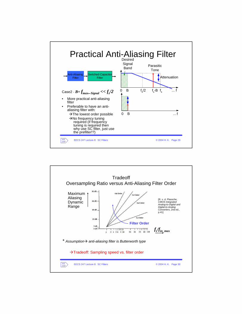
EECS 247 Lecture 8: SC Filters © 2004 H. K. Page 29A/DDSP
Practical Anti-Aliasing Filter
0 fs ... f
DesiredSignalBand
fs/2B fs-B
ParasiticTone
Attenuation
0 ... fB
Anti-Aliasing Filter
Switched-CapacitorFilter
Case2 - B= fmax_Signal << fs/2• More practical anti-aliasing
filter• Preferable to have an anti-
aliasing filter with:àThe lowest order possibleàNo frequency tuning
required (if frequency tuning is required then why use SC filter, just use the prefilter!?)
EECS 247 Lecture 8: SC Filters © 2004 H. K. Page 30A/DDSP
TradeoffOversampling Ratio versus Anti-Aliasing Filter Order
àTradeoff: Sampling speed vs. filter order
Maximum Aliasing Dynamic Range
fs/fin_max
Filter Order
[R. v. d. Plassche, CMOS Integrated Analog-to-Digital and Digital-to-Analog Converters, 2nd ed., p.41]
* Assumptionà anti-aliasing filter is Butterworth type

EECS 247 Lecture 8: SC Filters © 2004 H. K. Page 31A/DDSP
Effect of Sample & Hold
p
p
s
p
fT
fT
T
TfH
π
π )sin()( =
......
Tp
Ts
......
Ts
Sample &Hold
•Using the Fourier transform of a rectangular impulse:
EECS 247 Lecture 8: SC Filters © 2004 H. K. Page 32A/DDSP
0 0.5 1 1.5 2 2.5 30
0.1
0.2
0.3
0.4
0.5
0.6
0.7
0.8
0.9
1
f / fs
abs(
H(f
))
Effect of Sample & Hold on
Frequency Response
p
p
s
p
fT
fT
T
TfH
π
π )sin(|)(| =
Tp=Ts
Tp=0.5Ts
More practical

EECS 247 Lecture 8: SC Filters © 2004 H. K. Page 33A/DDSP
Sample & Hold Effect (Reconstruction of Analog Signals)
Time domain
timevolt a
ge
ZOH
fs …….. f
Am
plitu
de
fin 2fs
Frequency domainsin( )( )
fTsH ffTs
π
π=
Tp=Ts
Magnitude droop due to sinx/xeffect
EECS 247 Lecture 8: SC Filters © 2004 H. K. Page 34A/DDSP
Sample & Hold Effect (Reconstruction of Analog Signals)
Time domain
timevolta
ge
fs f
Am
plitu
de
fin
Frequency domain
Magnitude droop due to sinx/x effect:
Case 1) fsig=fs /4
Droop= -1dB
-1dB

EECS 247 Lecture 8: SC Filters © 2004 H. K. Page 35A/DDSP
Sample & Hold Effect (Reconstruction of Analog Signals)
Time domainMagnitude droop due to sinx/x effect:
Case 2) fsig=fs /32
Droop= -0.0035dB
à High oversampling ratio desirable
fs f
Am
plitu
de
fin
Frequency domain-0.0035dB
0 0.5 1 1.5 2 2.5 3 3.5
x 10-5
-1
-0.8
-0.6
-0.4
-0.2
0
0.2
0.4
0.6
0.8
1
Time
Am
plitu
de
sampled dataafter ZOH
EECS 247 Lecture 8: SC Filters © 2004 H. K. Page 36A/DDSP
Summary
• Sampling theorem à fs > 2fmax_Signal
• Signals at frequencies nfS± fsig fold back down to desired signal band, fsig
à This is called aliasing & usually dictates use of anti-aliasing pre-filters
• Oversampling helps reduce order of anti-aliasing filter
• S/H function shapes the frequency response with sinx/x
à Need to pay attention to droop in passband due to sinx/x
• If the above requirements is not met, CT signal can NOT be recovered from SD or DT without loss of information

EECS 247 Lecture 8: SC Filters © 2004 H. K. Page 37A/DDSP
1st Order FilterTransient Analysis
SC response:extra delay and steps withfinite rise time.Impractical
No problem
exaggerated
EECS 247 Lecture 8: SC Filters © 2004 H. K. Page 38A/DDSP
1st Order FilterTransient Analysis
ZOH
• ZOH: pick signal after settling(usually at end of clock phase)
• Adds delay and sin(x)/x distortion• When in doubt, use a ZOH in
periodic ac simulations

EECS 247 Lecture 8: SC Filters © 2004 H. K. Page 39A/DDSP
Periodic AC Analysis
EECS 247 Lecture 8: SC Filters © 2004 H. K. Page 40A/DDSP
Magnitude Response
1. RC filter output2. SC output after ZOH3. Input after ZOH4. Corrected output
• (2) over (3)• Repeats filter shape
around nfs• Identical to RC for
f <<fs/2
RC filter output
SC output after ZOH
Corrected output no ZOH
Sinc
fs 2fs 3fs

EECS 247 Lecture 8: SC Filters © 2004 H. K. Page 41A/DDSP
Periodic AC Analysis
• SPICE frequency analysis– ac linear, time-invariant circuits– pac linear, time-variant circuits
• SpectreRF statementsV1 ( Vi 0 ) vsource type=dc dc=0 mag=1 pacmag=1PSS1 pss period=1u errpreset=conservativePAC1 pac start=1 stop=1M lin=1001
• Output– Divide results by sinc(f/fs) to correct for ZOH distortion
EECS 247 Lecture 8: SC Filters © 2004 H. K. Page 42A/DDSP
Spectre Circuit Filerc_pacsimulator lang=spectreahdl_include "zoh.def"
S1 ( Vi c1 phi1 0 ) relay ropen=100G rclosed=1 vt1=-500m vt2=500mS2 ( c1 Vo_sc phi2 0 ) relay ropen=100G rclosed=1 vt1=-500m vt2=500mC1 ( c1 0 ) capacitor c=314.159fC2 ( Vo_sc 0 ) capacitor c=1pR1 ( Vi Vo_rc ) resistor r=3.1831MC2rc ( Vo_rc 0 ) capacitor c=1pCLK1_Vphi1 ( phi1 0 ) vsource type=pulse val0=-1 val1=1 period=1u
width=450n delay=50n rise=10n fall=10nCLK1_Vphi2 ( phi2 0 ) vsource type=pulse val0=-1 val1=1 period=1u
width=450n delay=550n rise=10n fall=10nV1 ( Vi 0 ) vsource type=dc dc=0 mag=1 pacmag=1PSS1 pss period=1u errpreset=conservativePAC1 pac start=1 stop=3.1M log=1001ZOH1 ( Vo_sc_zoh 0 Vo_sc 0 ) zoh period=1u delay=500n aperture=1n tc=10pZOH2 ( Vi_zoh 0 Vi 0 ) zoh period=1u delay=0 aperture=1n tc=10p

EECS 247 Lecture 8: SC Filters © 2004 H. K. Page 43A/DDSP
ZOH Circuit File// Copy from the SpectreRF Primer
module zoh (Pout, Nout, Pin, Nin) (period, delay, aperture, tc)
node [V,I] Pin, Nin, Pout, Nout;parameter real period=1 from (0:inf);parameter real delay=0 from [0:inf);parameter real aperture=1/100 from (0:inf);parameter real tc=1/500 from (0:inf);integer n; real start, stop;node [V,I] hold;analog // determine the point when aperture beginsn = ($time() - delay + aperture) / period + 0.5;start = n*period + delay - aperture;$break_point(start);
// determine the time when aperture endsn = ($time() - delay) / period + 0.5;stop = n*period + delay;$break_point(stop);
// Implement switch with effective series // resistence of 1 Ohmif ( ($time() > start) && ($time() <= stop))I(hold) <- V(hold) - V(Pin, Nin);
elseI(hold) <- 1.0e-12 * (V(hold) - V(Pin, Nin));
// Implement capacitor with an effective // capacitance of tcI(hold) <- tc * dot(V(hold));
// Buffer outputV(Pout, Nout) <- V(hold);
// Control time step tightly during // aperture and loosely otherwiseif (($time() >= start) && ($time() <= stop))$bound_step(tc);
else$bound_step(period/5);
EECS 247 Lecture 8: SC Filters © 2004 H. K. Page 44A/DDSP
time
Vo
Output Frequency Spectrum
Antialiasing Pre-filter
fs 2fsf-3dB
First Order S.C. Filter
Vin Vout
C1
S1 S2
φ1 φ2
C2
Vin time
Switched-Capacitor Filters à problem with aliasing

EECS 247 Lecture 8: SC Filters © 2004 H. K. Page 45A/DDSP
Antialiasing Pre-filter
fs 2fsf-3dB
Example : Anti-Aliasing Filter
• Voice-band SC filter f-3dB =4kHz & fs =256kHz • Anti-aliasing filter requirements:
– Need 40dB attenuation at clock freq. – Incur no phase-error from 0 to 4kHz– Gain error 0 to 4kHz < 0.05dB– Allow +-30% variation for anti-aliasing corner frequency (no tuning)à2-pole Butterworth LPF with nominal corner freq. of 17kHz & no
tuning (12kHz to 22kHz corner frequency )
Ease of anti-aliasing à high ratio for fsampling / f-3dB
EECS 247 Lecture 8: SC Filters © 2004 H. K. Page 46A/DDSP
Switched-Capacitor Noise
• Resistance of switch S1 produces a noise voltage on C with variance kT/C
• The corresponding noise charge is Q2=C2V2=kTC
• This charge is sampled when S1 opens
vIN vOUT
CS1 S2
φ1 φ2
φ1
φ2
T=1/fs

EECS 247 Lecture 8: SC Filters © 2004 H. K. Page 47A/DDSP
Switched-Capacitor Noise
• Resistance of switch S2 contributes to an uncorrelated noise charge on C at the end of φ2
• Mean-squared noise charge transferred from vIN to vOUT each sample period is Q2=2kTC
vIN vOUT
CS1 S2
φ1 φ2
φ1
φ2
T=1/fs
EECS 247 Lecture 8: SC Filters © 2004 H. K. Page 48A/DDSP
• The mean-squared noise current due to S1 and S2’s kT/C noise is :
• This noise is approximately white and distributed between 0 and fs/2(noise spectra à single sided by convention) The spectral density of the noise is:
à S.C. resistor noise equals a physical resistor noise with same value!
Switched-Capacitor Noise
( )22 2s B si Q f 2k TCf= =
c
22
B s BB s E Q
E Q ss
2k T C 4k Ti 14k T C f u s i n g R
f R f C2
ff= = = =
∆

EECS 247 Lecture 8: SC Filters © 2004 H. K. Page 49A/DDSP
Periodic Noise Analysis
PSS pss period=100n maxacfreq=1.5G errpreset=conservativePNOISE ( Vrc_hold 0 ) pnoise start=0 stop=20M lin=500 maxsideband=10
ZOH1T = 100ns
ZOH1T = 100ns
S1R100kOhm
R100kOhm
C1pFC1pF
PNOISE Analysissweep from 0 to 20.01M (1037 steps)
PNOISE1
Netlistahdl_include "zoh.def"ahdl_include "zoh.def"
Vclk100ns
Vrc Vrc_hold
Sampling Noise from SC S/H
C11pFC11pFC11pFC11pF
R1100kOhm
R1100kOhm
R1100kOhm
R1100kOhm
Voltage NOISEVNOISE1
NetlistsimOptions options reltol=10u vabstol=1n iabstol=1psimOptions options reltol=10u vabstol=1n iabstol=1psimOptions options reltol=10u vabstol=1n iabstol=1psimOptions options reltol=10u vabstol=1n iabstol=1p
SpectreRF PNOISE: checknoisetype=timedomainnoisetimepoints=[…]
as alternative to ZOH.noiseskipcount=large
might speed up things in this case.
EECS 247 Lecture 8: SC Filters © 2004 H. K. Page 50A/DDSP
Sampled Noise Spectrum
Density of sampled noise with sinc distortion.
Normalized density of sampled noise, corrected for sinc distortion.
EECS 247 Lecture 8: SC Filters © 2004 H. K. Page 51A/DDSP
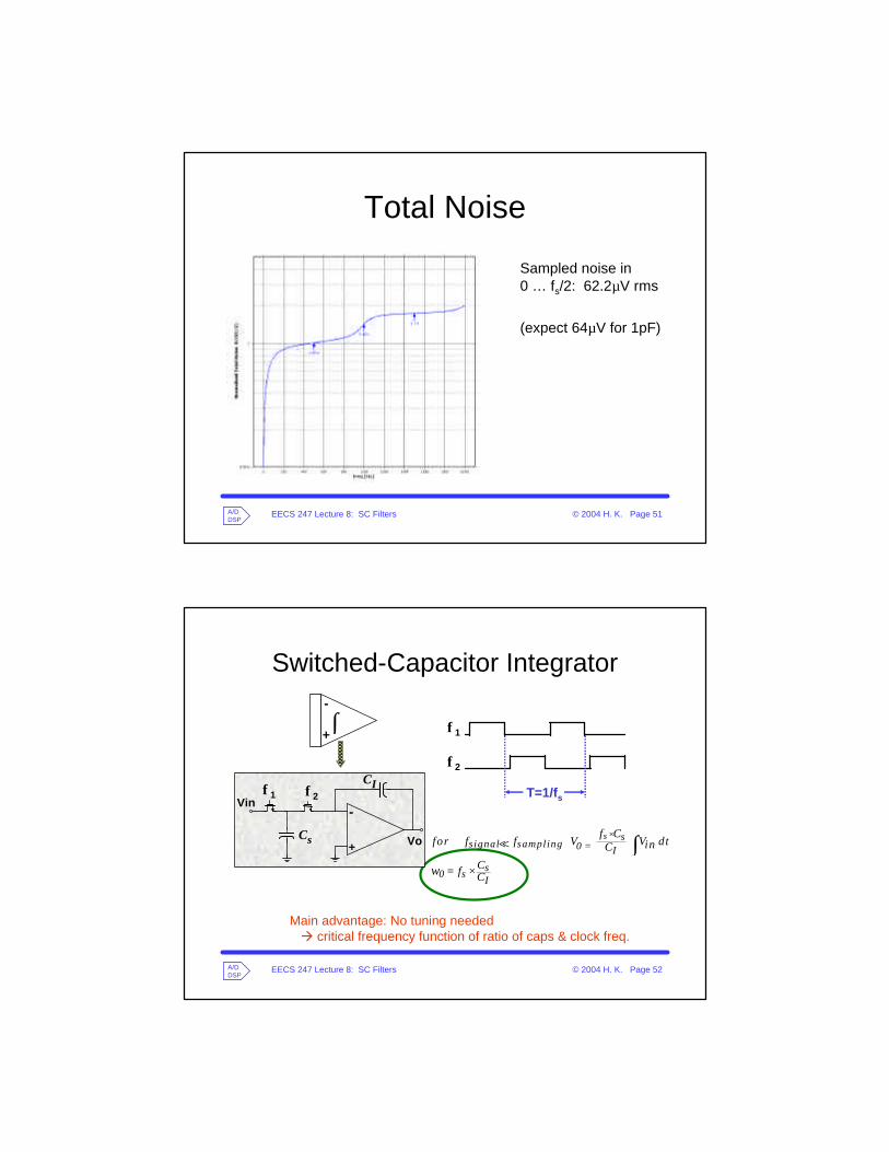
Total Noise
Sampled noise in 0 … fs/2: 62.2µV rms
(expect 64µV for 1pF)
EECS 247 Lecture 8: SC Filters © 2004 H. K. Page 52A/DDSP
Switched-Capacitor Integrator
-
+
Vin
Vo
φ1 φ2
CI
Cs s ssignal sampling 0 I
s0 sI
f Cfor f f V V dtinC
Cf Cω
×=
= ×
∫=
-
+∫ φ1
φ2
T=1/fs
Main advantage: No tuning needed à critical frequency function of ratio of caps & clock freq.
EECS 247 Lecture 8: SC Filters © 2004 H. K. Page 53A/DDSP
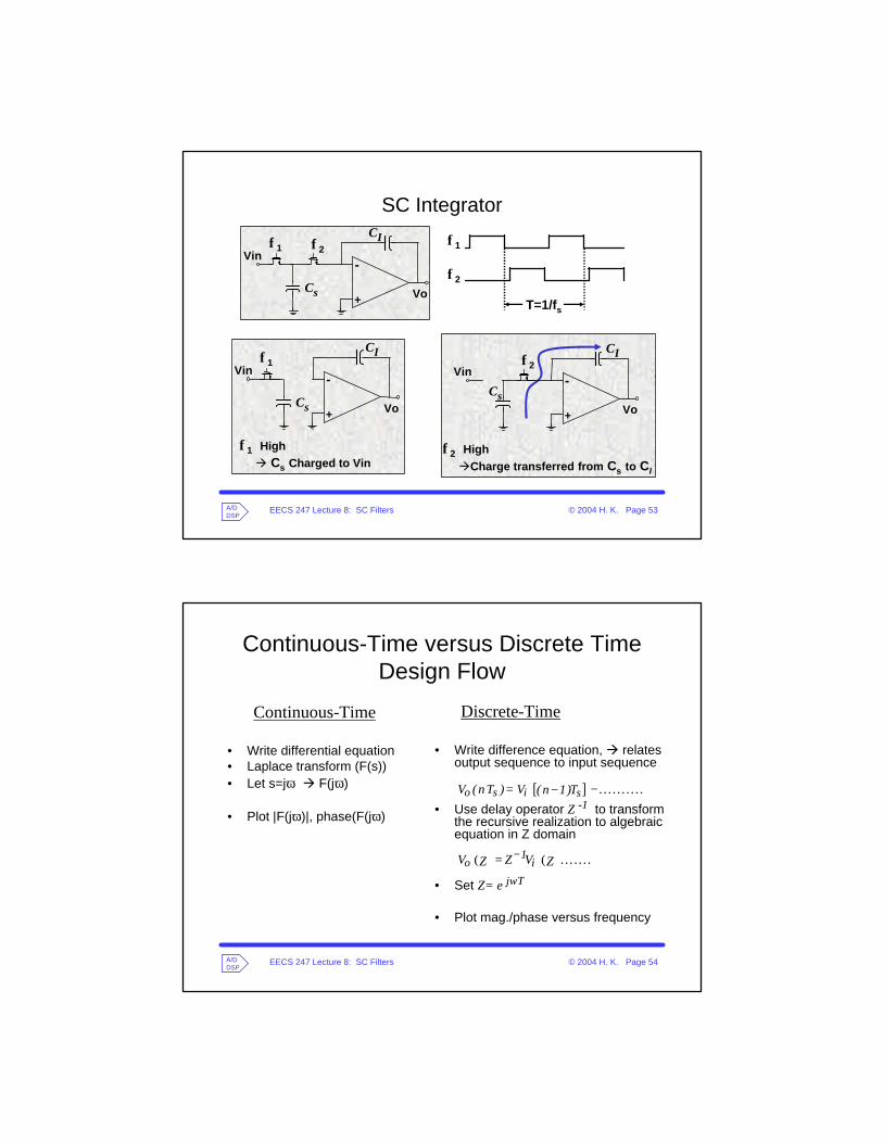
SC Integrator
-
+
Vin
Vo
φ1 φ2
CI
Cs
-
+
Vin
Vo
φ1
CI
Cs
-
+
Vin
Vo
φ2
CI
Cs
φ1
φ2
T=1/fs
φ1 High à Cs Charged to Vin
φ2 HighàCharge transferred from Cs to CI
EECS 247 Lecture 8: SC Filters © 2004 H. K. Page 54A/DDSP
Continuous-Time versus Discrete Time Design Flow
Continuous-Time
• Write differential equation• Laplace transform (F(s))• Let s=jω à F(jω)
• Plot |F(jω)|, phase(F(jω)
Discrete-Time
• Write difference equation, à relates output sequence to input sequence
• Use delay operator Z -1 to transform the recursive realization to algebraic equation in Z domain
• Set Z= e jωT
• Plot mag./phase versus frequency
[ ]
( ) ( )
o s i s
1o i
V (nT ) V . . . . . . . . . .( n 1)T
V Z V .. . . . . .Z Z−
= −−
=

EECS 247 Lecture 8: SC Filters © 2004 H. K. Page 55A/DDSP
SC Integrator
-
+
Vin
Vo
φ1 φ2
CI
Cs
Vs
φ1 φ2 φ1 φ2φ1
Vin
Vo
Vs
Clock
EECS 247 Lecture 8: SC Filters © 2004 H. K. Page 56A/DDSP
φ1 φ2 φ1 φ2φ1
Vin
Vo
Vs
Clock
SC Integrator(n-1)Ts nTs(n-1/2)Ts (n+1)Ts
Φ1 à Qs [(n-1)Ts]= Cs Vi [(n-1)Ts] , QI [(n-1)Ts] = QI[(n-3/2)Ts]
Φ2 à Qs [(n-1/2) Ts] = 0 , QI [(n-1/2) Ts] = QI [(n-3/2) Ts] + Qs [(n-1) Ts]
Φ1 _à Qs [nTs ] = Cs Vi [nTs ] , QI [nTs ] = QI[(n-1) Ts ] + Qs [(n-1) Ts]
Since Vo= - QI /CI & Vi = Qs / Csà CI Vo(nTs) = CI Vo [(n-1) Ts ] -Cs Vi [(n-1) Ts ]
(n-3/2)Ts

EECS 247 Lecture 8: SC Filters © 2004 H. K. Page 57A/DDSP
Discrete Time Design Flow
• Transforming the recursive realization to algebraic equation in Z domain:– Use Delay operator Z :
s1s1/ 2s1s1/ 2s
nT ..................... 1............. Z( n 1)T
.......... Z( n 1/ 2 )T
............. Z( n 1)T
.......... Z( n 1/ 2 )T
−
−
+
+
→→−
→−→+
→+
EECS 247 Lecture 8: SC Filters © 2004 H. K. Page 58A/DDSP
SC Integrator
sIsI
1s1I
o s o ss sI I inCo s o s sinCC1 1o o inC
CC 1
in
C V (nT ) C V C V( n 1)T ( n 1)T
V (nT ) V V( n 1)T ( n 1)T
V ( Z ) Z V ( Z ) Z V ( Z )
Vo Z( Z )ZV
−−
− −
−
− = − +− −
= −− −
= −
= − ×
DDI (Direct-Transform Discrete Integrator)
-
+
Vin
Vo
φ1 φ2
CI
Cs
φ1

EECS 247 Lecture 8: SC Filters © 2004 H. K. Page 59A/DDSP
z-Plane
• Consider variable Z=esT for any s in left-half-plane (LHP):
S= - a+jbZ= e-aT . e jbT = e-aT (cosbT + jsin bT)
|Z|= e-aT , angle(Z)= bTà For values of S in LHP |Z|<1à For a =0 (imag. axis in s-plane) |Z|=1 (unit circle)
if angle(Z)=π=bT then b=π/T=ωThen ω=ωs/2
EECS 247 Lecture 8: SC Filters © 2004 H. K. Page 60A/DDSP
z-Domain Frequency Response• LHP singularities in
s-plane map into inside of unit-circle in Z domain
• RHP singularities in s-plane map into outside of unit-circle in Z domain
• The jω axis maps onto the unit circle
LHP in s domain
Z plane imag. axis in s domain

EECS 247 Lecture 8: SC Filters © 2004 H. K. Page 61A/DDSP
z-Domain Frequency Response
• Particular values:– f = 0 à z = 1– f = fs/2 à z = -1
• The frequency response is obtained by evaluating H(z) on the unit circle at z = ejωT = cos(ωT)+jsin(ωT)
• Once z=1 (fs/2) is reached, the frequency response repeats, as expected
(cos(ωT),sin(ωT))
f = 0
f = fs/2
EECS 247 Lecture 8: SC Filters © 2004 H. K. Page 62A/DDSP
z-Domain Frequency Response• The angle to the
pole is equal to 360° (or 2π radians) times the ratio of the pole frequency to the sampling frequency
(cos(ωT),sin(ωT))
2πffS
f = 0
f = fs/2

EECS 247 Lecture 8: SC Filters © 2004 H. K. Page 63A/DDSP
s-Plane versus z-PlaneExample: 2nd Order LDI Bandpass Filter
σ
jωs-plane z-plane
EECS 247 Lecture 8: SC Filters © 2004 H. K. Page 64A/DDSP
Pole-Zero Map in z-PlaneZero from fàinfinityin s-plane mapped to z=0, a non-physical frequency.
Zero from fà0in s-plane mapped to z=+1
Distance from the pole to the unit circle is inversely proportional to pole Q
Pole on unit-circle à Q of infinity
z-plane

EECS 247 Lecture 8: SC Filters © 2004 H. K. Page 65A/DDSP
DDI SC IntegratorCI
Ideal Integrator) Magnitude Error Phase Error
( )
( )
1s1I
j T / 2s sj T j T / 2 j T / 2I I
sI
sI
C j TC 1
in
C CC C1
C j T / 2C
C j T / 2C j T
Vo Z( Z ) , Z eZV
e1e e e
1j e 2sin T / 2
T / 21 esin T / 2
ωω ω ω
ω
ω
ω
ω
ωω ω
−−
−−
−
− −
−
−
= − × =
= × = ×
= − × ×
= − × ×
-
+
Vin
Vo
φ1 φ2
CI
Cs
φ1
EECS 247 Lecture 8: SC Filters © 2004 H. K. Page 66A/DDSP
DDI SC IntegratorCI
Ideal Integrator) Magnitude Error Phase Error( )
sI
C j T / 2C j T
in
V T / 2o 1( Z ) esin T / 2V
ωωω ω
−= − × ×
-
+
Vin
Vo
φ1 φ2
CI
Cs
φ1
Example: Mag. & phase error for:1- f / fs=1/12 àMag. Error = 1% or 0.1dB
Phase error=15 degreeQintg = -3.8
2- f / fs=1/32 àMag. Error=0.16% or 0.014dBPhase error=5.6 degreeQintg = -10.2
DDI Integratorà magnitude error no problem
phase error major problem

EECS 247 Lecture 8: SC Filters © 2004 H. K. Page 67A/DDSP
SC Integrator
CI
-
+
Vin
Vo
φ1 φ2
CI
Cs
φ2
Sample output ½ clock cycle earlier
à Sample output on φ2
EECS 247 Lecture 8: SC Filters © 2004 H. K. Page 68A/DDSP
φ1 φ2 φ1 φ2φ1
Vin
Vo
Vs
Clock
SC Integrator(n-1)Ts nTs(n-1/2)Ts (n+1)Ts
Φ1 à Qs [(n-1)Ts]= Cs Vi [(n-1)Ts] , QI [(n-1)Ts] = QI[(n-3/2)Ts]
Φ2 à Qs [(n-1/2) Ts] = 0 , QI [(n-1/2) Ts] = QI [(n-3/2) Ts] + Qs [(n-1) Ts]
Φ1 _à Qs [nTs ] = Cs Vi [nTs ] , QI [nTs ] = QI[(n-1) Ts ] + Qs [(n-1) Ts]
Φ2 à Qs [(n+1/2) Ts] = 0 , QI [(n+1/2) Ts] = QI [(n-1/2) Ts] + Qs [n Ts]
(n-3/2)Ts