Embed Size (px)
Citation preview
Bias-Line Compensation in Multi-Stage Amplifiers
Punith R. Surkanti and Paul M. Furth
Klipsch School of Electrical and Computer Engineering,
New Mexico State University, Las Cruces, NM 88003, USA
Email: [email protected], [email protected]
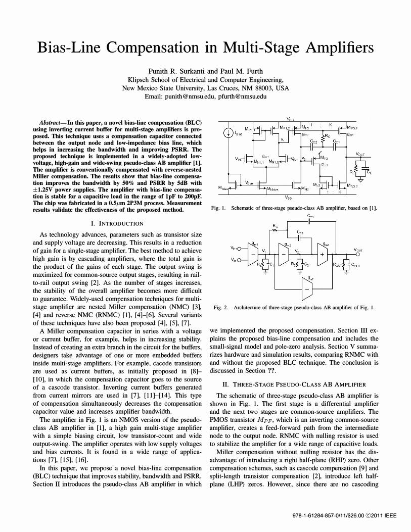
Abstract- In this paper, a novel bias-line compensation (BLC) using inverting current buffer for multi-stage amplifiers is proposed. This technique uses a compensation capacitor connected between the output node and low-impedance bias line, which helps in increasing the bandwidth and improving PSRR. The proposed technique is implemented in a widely-adopted lowvoltage, high-gain and wide-swing pseudo-class AB amplifier [1]. The amplifier is conventionally compensated with reverse-nested Miller compensation. The results show that bias-line compensation improves the bandwidth by 50% and PSRR by 5dB with ±1.25V power supplies. The amplifier with bias-line compensation is stable for a capacitive load in the range of IpF to 200pF. The chip was fabricated in a 0.5JLm 2P3M process. Measurement results validate the effectiveness of the proposed method. Fig. I. Schematic of three-stage pseudo-class AB amplifier, based on [1].
I. INTRODUCTION
As technology advances, parameters such as transistor size
and supply voltage are decreasing. This results in a reduction
of gain for a single-stage amplifier. The best method to achieve
high gain is by cascading amplifiers, where the total gain is
the product of the gains of each stage. The output swing is
maximized for common-source output stages, resulting in rail
to-rail output swing [2]. As the number of stages increases,
the stability of the overall amplifier becomes more difficult
to guarantee. Widely-used compensation techniques for multi
stage amplifier are nested Miller compensation (NMC) [3],
[4] and reverse NMC (RNMC) [ 1], [4]-[6]. Several variants
of these techniques have also been proposed [4], [5], [7].
A Miller compensation capacitor in series with a voltage
or current buffer, for example, helps in increasing stability.
Instead of creating an extra branch in the circuit for the buffers,
designers take advantage of one or more embedded buffers
inside multi-stage amplifiers. For example, cacode transistors
are used as current buffers, as initially proposed in [8]
[ 10], in which the compensation capacitor goes to the source
of a cascode transistor. Inverting current buffers generated
from current mirrors are used in [7], [ 1 1]-[ 14]. This type
of compensation simultaneously decreases the compensation
capacitor value and increases amplifier bandwidth.
The amplifier in Fig. 1 is an NMOS version of the pseudo
class AB amplifier in [ 1], a high gain multi-stage amplifier
with a simple biasing circuit, low transistor-count and wide
output-swing. The amplifier operates with low supply voltages
and bias currents. It is found in a wide range of applica
tions [7], [ 15], [ 16].
In this paper, we propose a novel bias-line compensation
(BLC) technique that improves stability, bandwidth and PSRR.
Section II introduces the pseudo-class AB amplifier in which
Fig. 2. Architecture of three· stage pseudo·c1ass AB amplifier of Fig. 1.
we implemented the proposed compensation. Section III ex
plains the proposed bias-line compensation and includes the
small-signal model and pole-zero analysis. Section V summa
rizes hardware and simulation results, comparing RNMC with
and without the proposed BLC technique. The conclusion is
discussed in Section ??
II. THREE-STAGE PSEUDO-CLASS AB AMPLIFIER
The schematic of three-stage pseudo-class AB amplifier is
shown in Fig. 1. The first stage is a differential amplifier
and the next two stages are common-source amplifiers. The
PMOS transistor MpF, which is an inverting common-source
amplifier, creates a feed-forward path from the intermediate
node to the output node. RNMC with nulling resistor is used
to stabilize the amplifier for a wide range of capacitive loads.
Miller compensation without nulling resistor has the dis
advantage of introducing a right half-plane (RHP) zero. Other
compensation schemes, such as cascode compensation [9] and
split-length transistor compensation [2], introduce left half
plane (LHP) zeros. However, since there are no cascoding
978-1-61284-857-0/11/$26.00 <92011 IEEE

transistors in Fig. 1, using cascode compensation would nec
essarily increase static power and transistor count. Moreover,
both cascode and split-length transistor compensation have
no simple means of moving a LHP zero so as to cancel
an undesirable non-dominant pole. Miller compensation with
nulling resistor not only moves the RHP zero to the LHP, but
also offers freedom in selecting the exact location of the zero.
Fig. 2 is the small-signal architecture of the pseudo
class AB amplifier shown in Fig. 1. Parameters gMt. gM2, gM3 and g M F refer to the transconductance of the first, second,
third and feed-forward stages, respectively. The impedance at
the output of the first-stage VI are RIIICI, at the output of
the second-stage V2 are R211C2 and at the output of the final
stage VOUT are ROUTIICoUT. The gain of the amplifier is
the product of gains of all the cascade stages, as in
ADC = gMIRI· (gM2R2· gM3ROUT + gMFROUT). (1)
The amplifier has four poles. Compensation capacitance
CCI creates the dominant pole. The effect of the next two
non-dominant poles can be nullified by proper adjustment of
the two LHP zeros created by RNMC. The fourth pole is
at very high frequencies. As a result, the overall amplifier
response can be designed to behave as a single-pole system.
The equations of all the poles and zeros are shown in Table I.
III. PROPOSED BIAS-LINE COMPENS ATION TECHNIQUE
The proposed bias-line compensation (BLC) technique con
sists of negative feedback through a capacitor from the output
node to the bias-line. The bias transistor MN2 of the second
stage common-source amplifier acts as an inverted current
buffer. The three-stage pseudo-class AB amplifier shown in
Fig. 1 is initially compensated with RNMC. Bias-line compen
sation is applied to the amplifier with the addition of capacitor
CCB from the output node VOUT to the bias-line VBias, as
shown in Fig. 3.
A. Inverting Current Buffer
The amplifier has three bias transistors. One is the diode
connected transistor Mbias, that generates a bias voltage for
the rest of the circuit through the node VBias. The second
transistor is the tail transistor MNbiasl of the differential
amplifier and the other is MN2, which is a current source for
the second-stage common-source amplifier. The compensation
capacitor CCB from the output node is connected to VBias line. Since the bias transistor MNbias is the tail transistor for
the differential amplifier, the compensation has no effect on
it. Though the compensation induces feedback current into
the tail transistor MNbias, the PMOS current-mirror inside the
differential amplifier cancels the effect.
On the other hand, bias transistor M N2 creates an effect on
node V2 with current induced by the compensation capacitor.
This creates a path from the output node to the internal node
V2 through compensation capacitor CCB. Transistor MN2 has
inverting gain from its gate V Bias to drain V2. Therefore,
the transistor MN2 acts as an inverted current-buffer. The
compensation behaves as a capacitor in series with an inverted
Inverting Current-Buffer
Fig. 3. Schematic of three-stage pseudo-class AB amplifier with proposed bias-line comQensation.
"in-
Fig. 4. Small-signal architecture of three-stage pseudo-class AB amplifier with proposed bias-line compensation.
current-buffer, connected between the output VOUT and the
intermediate node V2. Since the compensation capacitor is
connected to a diode-connected transistor Mbias, the input
resistance of the current buffer is 1/ g M C B .
B. Small-Signal Model
The small-signal model of the amplifier with the proposed
bias-line compensation is shown in Fig. 4. The gain of the
amplifier is unchanged from (1).
The equations of all the poles and zeros are computed in
Table I. The RNMC moves the dominant pole WPI to low
frequencies. The effect of two non-dominant LHP poles WP2 and WP3 are cancelled by properly adjusting location of two
dominant LHP zeros WZI and WZ2 created by the RNMC. The
bias-line compensation creates a third LHP zero. Therefore the
amplifier is approximated as a double-pole and single-zero sys
tem. The LHP zero is located before the high frequency non
dominant LHP pole. Fig. 5 shows the approximate pole/zero
locations. The zero created by the proposed compensation
helps in improving the phase margin and bandwidth of the
amplifier.
IV. F ABRIC ATED TEST CHIP
The amplifiers were designed and fabricated in O.5J.Lm 2P3M
process with the device dimensions mentioned in Table II. The
micrograph of the fabricated circuits of Fig. 1 and Fig. 3 are
shown in Fig. 6. The amplifiers in the chip contains an output
capacitance of lOpF. The chip was tested with supply voltages

TABLE I
EQUATIONS OF PSEUDO-CLASS AB AMPLIFIERS SHOWN IN FIG. I AND FIG. 3
Pseudo-Class AB Pseudo-Class AB with BLC Poles Zeros
Wpl = - RlCCl9M2R29M3ROUT Wzl = - RC<CCl +CC2)
W - _ 9M3CGJ p2 - CC2(CCl+COUT) W - _ 9M29M3(CCl +CC2) z2 - (9M2+9M3)CClCC2
W - 9M3(CGJ +COUT) p3 - - CCl CCOUT
W - 1 p4 - - RCCl
RNMCR
RNMCR+ BLC
Fig. 5. Diagram illustrating poles and zeros (not to scale).
± 1.25V and an input bias current of lOpA. The total quiescent
current is 170p,A.
TABLE II
DEVICE DIMENSIONS
Pseudo-class AB
MNI,I, MNI,2, MN2, J.�,m = 2 MN3,1 MpI,}' MpI,2, Mp2, f.�,m=2 Mp3
MN3 & MpF J.�& f.�,m = 8
Mbias g,m=l
MNbias J.�,m = 4
RCI 20kn
CCI, CC2 7.5pF, 7.5pF
CCB -
Pseudo-class AB with BLC
J.�,m=2
f.�,m=2
J.�& f.�,m = 8
J.�,m = 1
g,m=4
20kn
3pF, 3pF
3pF
V. SIMUL ATED AND EXPERIMENTAL RESULTS
The values of the compensation capacitor CCb CC2, and
Cc B are adjusted so as to achieve the same phase margin with
out CCB. It is found that the total compensation capacitance
(CC1 +CC2+CCB) is reduced from 15pF without CCB to 9pF
with CCB. The reduction in compensation capacitance and the
creation of third zero WZ3 results in increased bandwidth.
A. Simulated Results
The amplifier in open-loop configuration is simulated to
find the gain, bandwidth, phase margin and gain margin. The
frequency plot of the amplifier with inverted current-buffer
compensation is shown in Fig. 7. The plot clearly shows
the cancellation of non-dominant poles with the zeros and
therefore the phase plot is nearly constant in the mid-range
frequencies.
Poles
WpI = - RlCCl9M2R29M3ROUT
W - _ 9MZCGJ p2 - CC2COUT
Wp3 =- �
Zeros
WzI = - RC<CCl +CC2)
Wz2 = -gM3(C�l + c�z> Wz3=- �
-20 � O'o· ��I"'O I��I"'O
:��I"'O'''''''''�uL
lO'''''''''�"'-;--�'''''''.,--'-�'"'-;-�'""''''
FI·�qu�ur�· (Hz)
Fig. 7. Simulated frequency response of the amplifier with proposed compensation for variable load.
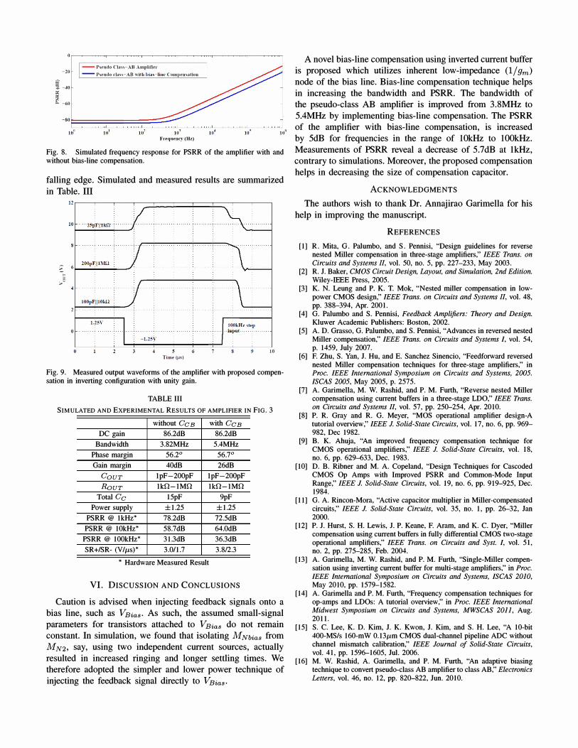
The simulated frequency plot of PSRR of the three-stage
amplifier with and without bias-line inverted current-buffer
compensation is shown in Fig. 8. From the waveforms, we
predict that PSRR is increased from 7-8 dB over a wide range
of frequencies.
B. Experimental Results
Transient measurements were performed for the amplifier
in inverting configuration. The input is a 100kHz square wave
with peak-to-peak voltage of 2.5Y. The amplifier was tested
for different combinations of load. Three of the combination
outputs are shown in Fig. 9. The measured slew rates of the
pseudo-class AB amplifier for a nominal load of lOk!11 I lOOpF
are 3.8V/p,s and 2.3V/p,s. Because of the difference in gains
of the feed-forward path and the three-stage path, the settling
time for the rising edge is higher than the settling time for the
-20
� -40 '" '" '" .. -60
- Pstudo Class-AB AmpUfifr
- Pst'udo class-AD ",lib blas-lIut' Compfusation
A novel bias-line compensation using inverted current buffer
is proposed which utilizes inherent low-impedance (l/gm) node of the bias line. Bias-line compensation technique helps
in increasing the bandwidth and PSRR. The bandwidth of
the pseudo-class AB amplifier is improved from 3.8MHz to
-80====�==::;:�==::������-,-,,-,,--;----,��
5.4MHz by implementing bias-line compensation. The PSRR
L,- of the amplifier with bias-line compensation, is increased 10° 101 I O! 103 lO� lOS 10'
r"'q"''''J' (Hz) by 5dB for frequencies in the range of 10kHz to 100kHz.
Fig. 8. Simulated frequency response for PSRR of the amplifier with and without bias-line compensation.
falling edge. Simulated and measured results are summarized
in Table. III
� 6
S >0
10 Timf'(J.ts)
Fig. 9. Measured output waveforms of the amplifier with proposed compensation in inverting configuration with unity gain.
TABLE III
SIMULATED AND EXPERIMENTAL RESULTS OF AMPLIFIER IN FIG. 3
without GCB with GCB DC gain 86.2dB 86.2dB
Bandwidth 3.82MHz 5.4MHz
Phase margin 56.2° 56.7°
Gain margin 40dB 26dB
GOUT IpF-200pF IpF-200pF
ROUT lkO-lMO lkO-lMO
Total Gc 15pF 9pF
Power supply ±1.25 ±1.25
PSRR @ 1kHz· 78.2dB n.5dB
PSRR @ 10kHz· 58.7dB 64.0dB
PSRR @ 100kHz· 31.3dB 36.3dB
SR+/SR- (V//l-s)· 3.0/1.7 3.812.3
• Hardware Measured Result
VI. DISCUSSION AND CONCLUSIONS
Caution is advised when injecting feedback signals onto a
bias line, such as VBias' As such, the assumed small-signal
parameters for transistors attached to V Bias do not remain
constant. In simulation, we found that isolating MNbias from
MN2, say, using two independent current sources, actually
resulted in increased ringing and longer settling times. We
therefore adopted the simpler and lower power technique of
injecting the feedback signal directly to VBias.
Measurements of PSRR reveal a decrease of 5.7dB at 1kHz,
contrary to simulations. Moreover, the proposed compensation
helps in decreasing the size of compensation capacitor.
ACKNOWLEDGMENT S
The authors wish to thank Dr. Annajirao Garimella for his
help in improving the manuscript.
[1]
[2]
[3]
[4]
[5]
[6]
REFERENCES
R. Mita, G. Palumbo, and S. Pennisi, "Design guidelines for reverse nested Miller compensation in three-stage amplifiers," IEEE Trans. on Circuits and Systems II, vol. 50, no. 5, pp. 227-233, May 2003. R. J. Baker, CMOS Circuit Design, Layout, and Simulation, 2nd Edition. Wiley-IEEE Press, 2005. K. N. Leung and P. K. T. Mok, "Nested miller compensation in lowpower CMOS design," IEEE Trans. on Circuits and Systems II, vol. 48, pp. 388-394, Apr. 2001. G. Palumbo and S. Pennisi, Feedback Amplifiers: Theory and Design. Kluwer Academic Publishers: Boston, 2002. A. D. Grasso, G. Palumbo, and S. Pennisi, "Advances in reversed nested Miller compensation," IEEE Trans. on Circuits and Systems I, vol. 54, p. 1459, July 2007. F. Zhu, S. Yan, 1. Hu, and E. Sanchez Sinencio, "Feedforward reversed nested Miller compensation techniques for three-stage amplifiers," in Proc. IEEE International Symposium on Circuits and Systems, 2005. ISCAS 2005, May 2005, p. 2575.
[7] A. Garimella, M. W. Rashid, and P. M. Furth, "Reverse nested Miller compensation using current buffers in a three-stage LDO," IEEE Trans. on Circuits and Systems II, vol. 57, pp. 250-254, Apr. 2010.
[8] P. R. Gray and R. G. Meyer, "MOS operational amplifier design-A tutorial overview," IEEE J. Solid-State Circuits, vol. 17, no. 6, pp. 969-982, Dec 1982.
[9] B. K. Ahuja, "An improved frequency compensation technique for CMOS operational amplifiers," IEEE J. Solid-State Circuits, vol. 18, no. 6, pp. 629-{)33, Dec. 1983.
[10] D. B. Ribner and M. A. Copeland, "Design Techniques for Cascoded CMOS Op Amps with Improved PSRR and Common-Mode Input Range," IEEE 1. Solid-State Circuits, vol. 19, no. 6, pp. 919-925, Dec. 1984.
[11] G. A. Rincon-Mora, "Active capacitor multiplier in Miller-compensated circuits," IEEE 1. Solid-State Circuits, vol. 35, no. 1, pp. 26-32, Jan 2000.
[12] P. 1. Hurst, S. H. Lewis, 1. P. Keane, F. Aram, and K. C. Dyer, "Miller compensation using current buffers in fully differential CMOS two-stage operational amplifiers," IEEE Trans. on Circuits and Syst. I, vol. 51, no. 2, pp. 275-285, Feb. 2004.
[13] A. Garimella, M. W. Rashid, and P. M. Furth, "Single-Miller compensation using inverting current buffer for multi-stage amplifiers," in Proc. IEEE International Symposium on Circuits and Systems, ISCAS 2010, May 2010, pp. 1579-1582.
[14] A. Garimella and P. M. Furth, "Frequency compensation techniques for op-amps and LDOs: A tutorial overview," in Proc. IEEE International Midwest Symposium on Circuits and Systems, MWSCAS 2011, Aug. 2011.
[15] S. C. Lee, K. D. Kim, 1. K. Kwon, 1. Kim, and S. H. Lee, "A 10-bit 4oo-MS/s 160-mW O.13/l-m CMOS dual-channel pipeline ADC without channel mismatch calibration," IEEE Journal of Solid-State Circuits, vol. 41, pp. 1596-1605, Jul. 2006.
[16] M. W. Rashid, A. Garimella, and P. M. Furth, "An adaptive biasing technique to convert pseudo-class AB amplifier to class AB," Electronics Letters, vol. 46, no. 12, pp. 820-822, Jun. 2010.