Embed Size (px)
Citation preview

External Use
TM
Program Model Differences
Between Power Architecture® and
ARM® Technologies
FTF-NET-F0143
A P R . 2 0 1 4
Satoshi Iida | Application Manager

TM
External Use 1
Session Introduction
This session highlights some of programming model differences between Power Architecture and ARM Architecture. The session will provide:
• A reference point for users of both architectures if they are familiar with one of the architectures
• Familiarity with a new architecture if users have not yet had exposure to it
• An understanding of the similarities and differences of the two architectures
• This is a two hour session
• Please ask questions as they arise
About Me
• I manage Application engineering for Freescale digital networking and have been working to lead the effort in working with ARM based products
TM
External Use 2
Session Objectives
• Understand some key differences between Power Architecture and
ARM Architecture versions
• Understand key programing models of Power Architecture and
ARM Architecture

TM
External Use 3
Agenda
• Architecture versions
• Registers and instruction sets
• Exception model
• Memory model
• Coprocessors
• Architecture extensions
• Endian
• ARM ISA

TM
External Use 4
e200 ↔ e300 ↔ e500 ↔ e500mc ↔ e5500 ↔ e6500 Cores
Relative Optimized Performance
• Frequency overlap allows for incremental performance boosts as required
− e6500 frequency range: 1.6 GHz –
− e5500 frequency range: 1.2 GHz – 2.2 GHz
− e500mc frequency range: 1 GHz – 1.5 GHz
− e500 frequency range: 533 MHz – 1.333 GHz
− e300 frequency range: 266 MHz – 667 Mhz
− e200 frequency range: 80 Mhz – 475GHz
e6500 Platform
• 64 bit ISA
• Back side L2
• Dual Precision FPU
e500 Platform
Each platform architecture leads to higher efficiency/cycle
• More efficient core
• Multi Thread support
• AltiVec™ SIMD vector processor
• Advanced power saving modes
e5500 Platform

TM
External Use 5
ARM Architecture: Core and Processor Family Overview
ARM Processor Family ARM Architecture Core C
lass
ic A
RM
ARM7 ARMv3 ARM700
ARM710
ARM710a
ARM11 ARMv6
ARM1136J
ARM1156T2
ARM1176JZ
ARM11MPCore
Emb
ed
de
d
Cortex-M
ARMv6-M Cortex-M0
Cortex-M1
ARMv7-M CortexM3
ARMv7E-M Cortex-M4
Re
al-T
ime
Cortex-R ARMv7-R
Cortex-R4
Cortex-R5
Cortex-R7
Ap
plic
atio
n
Cortex-A ARMv7-A
Cortex-A5
Cortex-A7
Cortex-A8
Cortex-A9
Cortex-A15
64
-bit
Co
re
Cortex-A50 ARMv8-A Cortex-A53
Cortex-A57

TM
External Use 6
Freescale Solutions Based on ARM Architecture
Example of ARM core device family:
ARM7, ARM9, ARM11, Cortex-M, Cortex-R and Cortex-A
Classic ARM Processors ARM11 − ARM11 (Freescale i.MX3x)
Application Processors Cortex-A − Cortex-A8 (Freescale i.MX5x)
− Cortex-A9 (Freescale i.MX6x)
− Cortex-A7 (Freescale LS1021)
− Cortex-A5x (Freescale LS2 family)
Embedded Microcontroller Cortex-M
- Cortex-M0 (Freescale Kinetis L)
- Cortex-M4 (Freescale Kinetis K)

TM
External Use 7
Agenda
• Architecture versions
• Registers and instruction sets
• Exception model
• Memory model
• Coprocessors
• Architecture extensions
• Endian
• ARM ISA

TM
External Use 8
Data Size and Instruction Sets
• Both Power and ARM technologies are RISC architectures
− Most instructions execute in a single cycle
− Both are superscalar cores with out-of-order execution and in-order completion
− (ARM) Every instruction can be conditionally executed
• e200, e300, e500, e500mc 603e and ARM Cortex v7 are 32-bit load / store architectures
− The only memory accesses allowed are loads and stores
− (Power) Most internal registers are 64 bits wide
• e5500, e6500 and ARM Cortex A5x are 64bit load/store architectures
• Most ARM cores support two instruction sets
− ARM 32-bit instruction set
− Thumb instruction set mixed 16-bit and some 32-bit

TM
External Use 9
Power Architecture User Mode Registers
GPR 31
GPR 1
GPR 0
63 0
CR
0 63
CTR
0 63
LR
0 63
XER
0 63
…
TBL
63
TBU
0 31
0
ACC
63
0
SPEFSCR
32 63
VRSAVE
32 63
Base
Category
GPR31 hi
GPR1 hi
GPR0 hi
31 0
… GPR 31
GPR 1
GPR 0
63 32
…
63 0
FPR0
FPR1
FPR31
FPSCR
32 63
…
VSCR
Floating Point Category
VR0
VR1
VR31
…
Vector Category 127 0
SPE Category
Embedded.Performance
Monitor Category:
13 PMRs
63
Alternate Time Base
Category
ATB (ATBU)
0 63

TM
External Use 10
ARM Register Set
• 37 registers in total
• 16 general purpose registers
• 20 banked register
• Registers are all 32 bits wide
• The registers are arranged into several banks, with the accessible bank being governed by the processor mode
• Some of the registers have special significance
− R13 – stack pointer (SP)
− R14- link registers (LR)
− R15 – 1 dedicated program counter (PC)
• Status registers
• 1 dedicated Current Program Status Register (CPSR)
• 5 dedicated Saved Program Status Register (SPSR)
• There are banked SPs, LRs, and SPSRs for each privileged mode
Banked out
registers
Current
mode
ARM state general purpose register and Program counter
User
mode
r0-r7,
r15 and
CPSR
User
mode
r0-r12,
r15 and
CPSR
User
mode
r0-r12,
r15 and
CPSR
User
mode
r0-r12,
r15 and
CPSR
User
mode
r0-r12,
r15 and
CPSR

TM
External Use 11
Thumb Register Set
• The Thumb state register set is a subset of the ARM state set
• 27 registers in total
• 11 general purpose registers
• 15 banked register
• Registers are all 32 bits wide
• The registers are arranged into several banks, with the accessible bank being governed by the processor mode
• Some of the registers have special significance
− R13 – stack pointer (SP)
− R14- link registers (LR)
− R15 – 1 dedicated program counter (PC)
• Status registers
• 1 dedicated Current Program Status Register (CPSR)
• 5 dedicated Saved Program Status Register (SPSR)
• There are banked SPs, LRs, and SPSRs for each privileged mode
Current
mode Banked out
registers
Thumb state general purpose register and Program counter
User
mode
r0-r7,
r15 and
CPSR
User
mode
r0-r7,
r15 and
CPSR
User
mode
r0-r7,
r15 and
CPSR
User
mode
r0-r7,
r15 and
CPSR
User
mode
r0-r7,
r15 and
CPSR
Thumb state r8-r12
are not available.
Only have access to
half of the general
purpose registers
TM
External Use 12
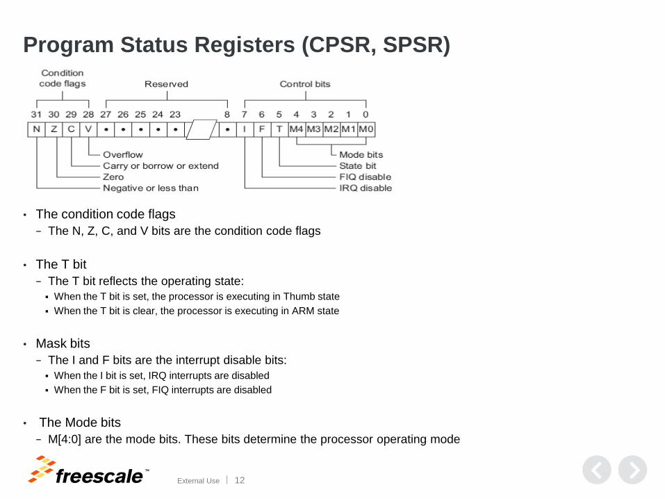
Program Status Registers (CPSR, SPSR)
• The condition code flags
− The N, Z, C, and V bits are the condition code flags
• The T bit
− The T bit reflects the operating state:
When the T bit is set, the processor is executing in Thumb state
When the T bit is clear, the processor is executing in ARM state
• Mask bits
− The I and F bits are the interrupt disable bits:
When the I bit is set, IRQ interrupts are disabled
When the F bit is set, FIQ interrupts are disabled
• The Mode bits
− M[4:0] are the mode bits. These bits determine the processor operating mode
TM
External Use 13
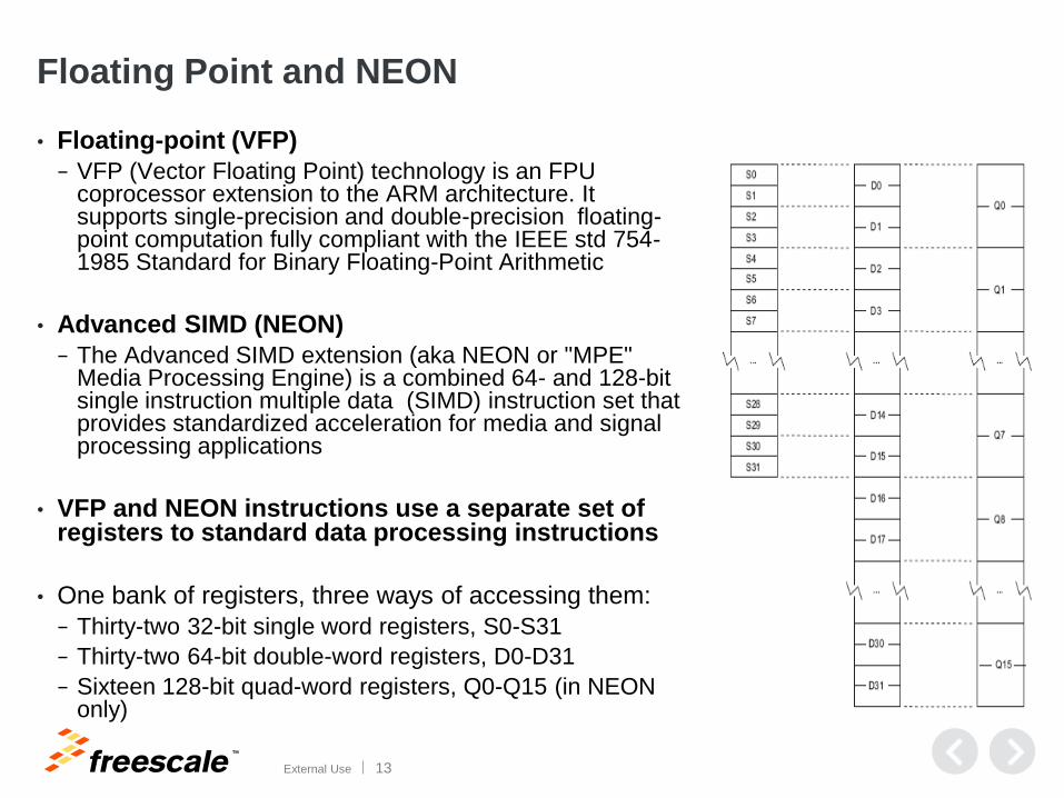
Floating Point and NEON
• Floating-point (VFP)
− VFP (Vector Floating Point) technology is an FPU coprocessor extension to the ARM architecture. It supports single-precision and double-precision floating-point computation fully compliant with the IEEE std 754-1985 Standard for Binary Floating-Point Arithmetic
• Advanced SIMD (NEON)
− The Advanced SIMD extension (aka NEON or "MPE" Media Processing Engine) is a combined 64- and 128-bit single instruction multiple data (SIMD) instruction set that provides standardized acceleration for media and signal processing applications
• VFP and NEON instructions use a separate set of registers to standard data processing instructions
• One bank of registers, three ways of accessing them:
− Thirty-two 32-bit single word registers, S0-S31
− Thirty-two 64-bit double-word registers, D0-D31
− Sixteen 128-bit quad-word registers, Q0-Q15 (in NEON only)

TM
External Use 14
Power ISA SIMD Numeric Acceleration
• AltiVec A 128-bit wide SIMD attacks parallel data-oriented compute
application
− 32, 128-bit vector registers
− 16 x 8, 8 x 16, 4 x 32-bit integer operations per clock
− 4 x 32-bit IEEE floating point operations per clock
− Powerful ‘permute’ unit (splats, shifts, rotates)
• Signal Processing Engine (SPE), area-efficient 64-bit SIMD
− 2-wide operations on 16- and 32-bit integers and fractions
− Embedded FP subcategories: Single, Double, and Vector (2 Single)
− Integer/fraction ops include saturating arithmetic
− Extends 32-bit GPRs to 64-bits
− Attacks DSP applications
Automotive powertrain: knock detect, signal conditioning, combustion modeling; uses
FIR’s, FFTs, Kalman filters
VoIP: convolutions, correlation, FIRs, excitation functions

TM
External Use 15
Signal Processing Engine GPRs Use
• GPRs are 64-bits, even though e500/e200 are 32-bit implementations
GPR
0 32 63
SPE lower
element
Normal 32-bit
Instructions
SPE upper
element
• Non category SPE instructions modify only
the lower 32 bits leaving the upper 32-bits
unchanged

TM
External Use 16
Embedded Floating Point
• Single-precision scalar and vector
• Double-precision scalar
• No FPRs: DP and vector SP use 64-bit extended GPRs. Scalar SP
uses lower word only in 32-bit implementations (as do non-SPE
instructions)
• Computation is saturating unless exceptions are enabled
• IEEE compliance requires software handlers for exceptions to
handle boundary conditions
• Found in the e200/e500

TM
External Use 17
Increased Code Density
• Cost is a key factor in some embedded applications − On-chip memory required to store software code is
inherently system cost
− Traditionally, RISC architectures have poorer code density than CISC architectures
• Book VLE (Variable Length Encoding) provides significant improvement in code density − Re-encoding of Power ISA instructions from
fixed 32-bit instructions into a mixture of 16- and 32-bit instructions
− 30% or greater code footprint reduction
− e200 family cores have best-in-class code density

TM
External Use 18
ARM Architecture Instruction Set Examples
Data processing instructions:
<operation><condition> Rd, Rm, <Op2> ADDEQ r4, r5, r6 ;r4 = r5 + r6
SUB r5, r7, #4 ;r5 = (r7 - #4)
MOV r4, #7 ;move immediate 7 into r4
Memory access instructions:
<operation><size> Rd, [<address>] LDR r0, [r6, #4] ; loading a 32 bit value
; adding 4 to address in r6
; loading the address result into r0
STRB r4,[r7], #8 ; storing a byte
; store the lower byte of r4 in to the address pointing to by r7
; then update r7 with 8
Program flow instructions:
<branch>{<condtion>} <label> <branch>{<condtion>} <sub_routine_label> B func_1 ; branch
BL func_2 ;branch with link
<operation>
<condition> Is an optional field. It specifies the condition under
which the instruction is executed.
<Op2> optional 2nd operand
<Rd> The destination register.
<Rm> The first operand register.
.

TM
External Use 19
Power Architecture Instruction Set Examples
Data processing instructions:
<operation> rD, rA, rB Add r4, r5, r6 ;r4 = r5 + r6
Subfic r5, r7, 0x4 ;r5 = (0x4 – r7)
addi r4, r0, 0x7 ;move immediate 7 into r4
Memory access instructions:
<operation><size> Rd, [<address>] lwz r0, 0x4(r6) ; loading a 32 bit value
; adding 4 to address in r6
; loading the address result into r0
stbu r4,0x8(r7) ; storing a byte
; store the lower byte of r4 in to the address pointing to by r7+0x8
; then update r7 with r7 + 0x8
Program flow instructions:
<branch>{<condtion>} <label> <branch>{<condtion>} <sub_routine_label> b func_1 ; branch
bl func_2 ; branch with link
<operation>
<rD> The destination register.
<rA rB> Source or destination general purpose register
SIMM/UIMM Signed/Unsigned immediate 16 bit value
.

TM
External Use 20
Agenda
• Architecture versions
• Registers and instruction sets
• Exception model
• Memory model
• Coprocessors
• Architecture extensions
• Endian
• ARM ISA

TM
External Use 21
Exceptions and Interrupts
• Interrupts
− Action where processor saves current context and begins execution at
predetermined interrupt handler
• Exceptions
− Events which cause the
processor to take an interrupt
Synchronous
Asynchronous
• Exception syndromes
− The ‘syndrome’ is the reason for the exception
Reported in the Exception Syndrome Register (ESR)
Exception
User
Privilege
Level
Supervisor
Privilege
Level
Context Switching
Errors,
Traps,
Interrupts
Applications NORMAL
rfi
Operating System (Exception Handlers)
TM
External Use 22
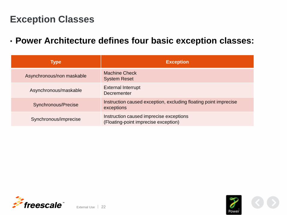
Exception Classes
• Power Architecture defines four basic exception classes:
Type Exception
Asynchronous/non maskable Machine Check
System Reset
Asynchronous/maskable External Interrupt
Decrementer
Synchronous/Precise Instruction caused exception, excluding floating point imprecise
exceptions
Synchronous/imprecise Instruction caused imprecise exceptions
(Floating-point imprecise exception)

TM
External Use 23
Interrupt Processing Power Architecture (e500)
Address SRR0/CSRR0/MCSRR0
Info on exception ESR/MESR
MSR SRR1/CSRR1/MCSRR1
MSR[SPE, WE, EE, PR,
RP, FE0 FE1, IS, DS] is
cleared for all interrupts
MSR[CE, DE] cleared only
for critical interrupts
MSR[ME] cleared only for
machine check
MSR
IVPR[32-47]||IVORn[48-
59]||0b0000 Instruction pointer

TM
External Use 24
IVOR

TM
External Use 25
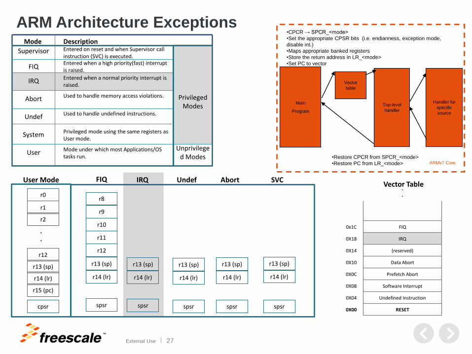
ARM Architecture Processor Modes
Processor
mode Abbreviations
Mode
encoding Privilege Description
USER usr 10000 Unprivileged Suitable for application code and other unprivileged processes.
FIQ fiq 10001 Privileged Entered as a result of a fast interrupt.
IRQ irq 10010 Privileged Entered as a result of a normal interrupt
Supervisor svc 10011 Privileged Suitable for running most kernel code.
Entered on Reset, and on execution of a Supervisor Call (SVC) instruction.
Abort abt 10111 Privileged Entered as a result of a Data Abort exception or Prefetch Abort exception.
Undefined und 11011 Privileged Entered as a result of an instruction-related error.
System SYS 11111 Privileged Suitable for processes that require privileged access to system resources, and for
privileged access to User mode registers
The ARM architecture defines seven basic modes:

TM
External Use 26
Vector Table
• The ARM architecture defines a
vector table containing a single
entry for each of the seven defined
exception types
• The size of the ARM vector table is
fixed at 8 words
• Each entry in the table is a single
executable ARM instruction which
is normally a branch instruction to
branch to the relevant exception
handler
• This vector table is located by
default at 0x0000:0000 or
0xFFFF:0000
0x0000:0000
IRQ
0 31
FIQ
(Reserved)
Data Abort
Software Interrupt
Prefetch Abort
Undefined Instruction
Reset
0x0000:0004
0x0000:0008
0x0000:000C
0x0000:0010
0x0000:0014
0x0000:0018
0x0000:001C
TM
External Use 27
FIQ
IRQ
(reserved)
Data Abort
Prefetch Abort
Software Interrupt
Undefined Instruction
RESET
0x1C
0X18
0X14
0X10
0X0C
0X08
0X04
0X00
Supervisor
IRQ
FIQ
Abort
Undef
System
User
Entered on reset and when Supervisor call instruction (SVC) is executed. Entered when a high priority(fast) interrupt is raised.
Entered when a normal priority interrupt is raised.
Used to handle memory access violations.
Used to handle undefined instructions.
Privileged mode using the same registers as User mode.
Mode under which most Applications/OS tasks run.
Privileged Modes
Unprivileged Modes
Mode Description
r0
r1
r2
r12
r13 (sp)
r14 (lr)
r15 (pc)
cpsr
.
.
User Mode
r13 (sp)
r14 (lr)
spsr
IRQ FIQ
spsr
Undef
spsr
Abort
spsr
SVC
r12
r13 (sp)
r14 (lr)
spsr
r9
r10
r11
r8
r13 (sp)
r14 (lr)
r13 (sp)
r14 (lr)
r13 (sp)
r14 (lr)
Vector Table .
.
.
Main
Program
Top-level
handler
Handler for
specific
source
•CPCR → SPCR_<mode>
•Set the appropriate CPSR bits (i.e. endianness, exception mode,
disable int.)
•Maps appropriate banked registers
•Store the return address in LR_<mode>
•Set PC to vector
ARMv7 Core
•Restore CPCR from SPCR_<mode>
•Restore PC from LR_<mode>
Vector
table
ARM Architecture Exceptions

TM
External Use 28
Agenda
• Architecture versions
• Registers and instruction sets
• Exception model
• Memory model
• Coprocessors
• Architecture extensions
• Endian
• ARM ISA
TM
External Use 29
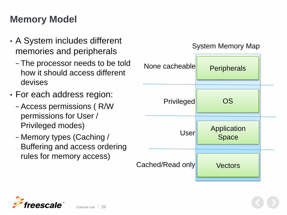
Memory Model
• A System includes different
memories and peripherals
− The processor needs to be told
how it should access different
devises
• For each address region:
− Access permissions ( R/W
permissions for User /
Privileged modes)
− Memory types (Caching /
Buffering and access ordering
rules for memory access)
OS
Peripherals
Application
Space
Vectors
None cacheable
System Memory Map
Privileged
User
Cached/Read only

TM
External Use 30
Power Architecture Memory Management Functions
• Address Translation
− Implements virtual memory
− Each process can have its own unique address space (232 for 32-bit
implementations or 264 for 64-bit implementations)
− Dynamic management of memory
• Protection and memory control
− Protection distinguishes between supervisor and user accesses
− Read, write, execute permissions
− Page attributes
Cache inhibited, write-through, guarded (speculative access protection)
Page size
Page types (normal, VLE, endianess)

TM
External Use 31
Evolution of the PowerPC to Power ISA Embedded MMU
PowerPC 1.10 MMU Power ISA 2.03 Embedded
Book III-E MMU
Segmented virtual address space
16 segment registers.
Unsegmented virtual address space No segment registers
Hardware managed TLB using hashed
reverse page tables
Software managed TLB H/W assist for TLB replacement No required page table format
Fixed 4KB sized pages
Variable sized translation via BATs Fixed and variable size pages supported
Separate instruction and data side TLB Unified instruction and data TLB
Real mode (translation off)
Virtual mode (translation on) No real mode (real mode can be emulated)

TM
External Use 32
Embedded Address Translation
Effective Page Address PID AS Offset
TLB
-multiple entry –
(real page number [RPN])
Real Page Number Offset
effective address
virtual address
64-bit real address
MSRDS for data accesses
MSRIS for instruction access

TM
External Use 33
Memory Management Registers
• Memory Management
− MMU Configuration Register (MMUCFG) – describes capabilities of
MMU such as number of TLB arrays, real address bits, etc.
− MMU Control and Status Register (MMUCSR0) – basic MMU controls
such as TLB invalidate-all and TLB page size
− TLB Configuration Registers (TLBnCFG) – describes capabilities of TLB
entries such as min and max page size, invalidation protect, number of
entries, associatively
− MMU Assist Registers (MASn) – used by software to read and write TLB
entries
− Process ID Registers (PIDn) – used by software as an address space
identifier to match TLB entries

TM
External Use 34
ARM Architecture Memory Types
• In ARM core architecture (ARMv6/ARMv7) address locations must be described in terms of
type
• The “type” tells the processor who can access that location
• There are three mutually exclusive memory types specified. These are: Normal, Device and
Strongly-ordered
• Normal and Device memory type have additional cache policy and whether the memory
region is shared.
Memory types
Normal Typically, memory used for program code and for data storage is Normal memory.
Device Memory map accesses to system are defined as Device/ peripherals.
Strongly- ordered A more restrictive accesses to memory-mapped regions. Examples of Strongly-ordered are memory-
mapped peripherals and I/O locations.(data used by legacy code)

TM
External Use 35
ARM Architecture - Memory Management Unit (MMU)
• MMU controls:
− Address translation
− Access permissions
− Memory attribute determination
• The Cortex-A7 includes a two stage MMU:
− First stage is owned by the guest OS (virtual to an intermediate physical
address IPA mapping)
− Second stage is owned by the hypervisor, and used for IPA to PA
mapping. Each software layer (OS and hypervisor) can manipulate
tables independent

TM
External Use 36
Data Alignment ( ARMv6/v7)
• ARM technology cores supporting architecture v6 and later are
capable of supporting unaligned accesses in hardware
− Data access can be unaligned
− Address marked as “Normal” can be accessed unaligned
• Load and store unit will access memory with aligned
memory access
TM
External Use 37
Agenda
• Architecture versions
• Registers and instruction sets
• Exception model
• Memory model
• Coprocessors
• Architecture extensions
• Endian
• ARM ISA
TM
External Use 38
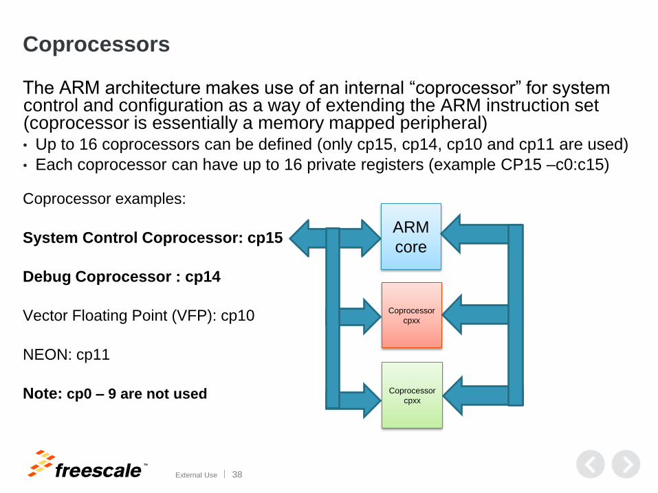
Coprocessors
The ARM architecture makes use of an internal “coprocessor” for system control and configuration as a way of extending the ARM instruction set (coprocessor is essentially a memory mapped peripheral) • Up to 16 coprocessors can be defined (only cp15, cp14, cp10 and cp11 are used)
• Each coprocessor can have up to 16 private registers (example CP15 –c0:c15)
Coprocessor examples:
System Control Coprocessor: cp15
Debug Coprocessor : cp14
Vector Floating Point (VFP): cp10
NEON: cp11
Note: cp0 – 9 are not used
ARM
core
Coprocessor
cpxx
Coprocessor
cpxx

TM
External Use 39
CP15.c1 registers
• CP15 c1, System Control Register (SCTLR)
• CP15 c1, Implementation defined Auxiliary Control Register (ACTLR)
• CP15 c1, Coprocessor Access Control Register (CPACR)
• CP15 c1, Secure Configuration Register (SCR)
• CP15 c1, Secure Debug Enable Register (SDER)
• CP15 c1, Non-Secure Access Control Register (NSACR)
Example: CP15.c1 from ARM TRM

TM
External Use 40
Example of CP15.c1 Register
CP15.c1, System Control Register (SCTLR)
• The SCTLR:
− Is a 32-bit read/write register, with different access rights for some bits of the register
− Is accessible only in privileged modes
− Has a defined reset value. The reset value is IMPLEMENTATION DEFINED
• TE, bit [30] Thumb Exception enable. This bit controls whether exceptions are taken in ARM or Thumb
• EE, bit [25] Exception Endianness bit. The value of this bit defines the value of the CPSR.E bit on entry to an exception vector, including reset
• V, bit [13] Vectors bit. This bit selects the base address of the exception vectors
• I, bit [12] Instruction cache enable bit: This is a global enable bit for instruction caches

TM
External Use 41
Agenda
• Architecture versions
• Registers and instruction sets
• Exception model
• Memory model
• Coprocessors
• Architecture extensions
• Endian
• ARM ISA

TM
External Use 42
Architecture Extensions
• TrustZone: (Secure_mode)
− The security of the system is achieved by partitioning all of the SoC’s hardware
and software resources so that they exist in one of two worlds - the Secure world
for the security subsystem, and the Normal world for everything else
• Virtualization: (Hypervisor_mode)
− Virtualization is a software security mechanism in which a highly trusted
management layer, known as a hypervisor, runs in a privileged mode of a
general purpose processor
Application Application
Guest OS Guest OS
Hypervisor
Normal World
Trusted Service
Trusted OS
Secure World
Secure
Monitor

TM
External Use 43
Agenda
• Architecture versions
• Registers and instruction sets
• Exception model
• Memory model
• Coprocessors
• Architecture extensions
• Endian
• ARM ISA
TM
External Use 44
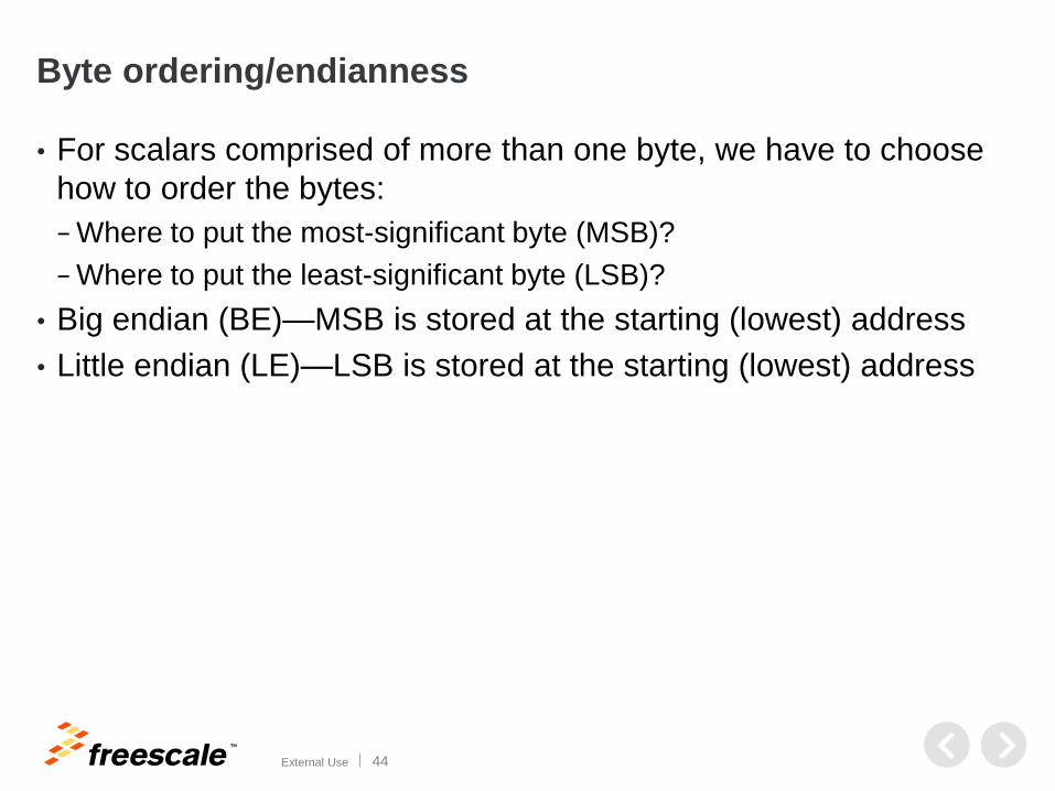
Byte ordering/endianness
• For scalars comprised of more than one byte, we have to choose
how to order the bytes:
− Where to put the most-significant byte (MSB)?
− Where to put the least-significant byte (LSB)?
• Big endian (BE)—MSB is stored at the starting (lowest) address
• Little endian (LE)—LSB is stored at the starting (lowest) address

TM
External Use 45
Big endian stores the MSB first
• Store a word in memory:
0x2021_2223
MSB LSB
• Putting the MSB first, memory looks like this:
20 21 22 23
[0] [1] [2] [3]
Increasing Address
[4] [5] [6] [7]
TM
External Use 46
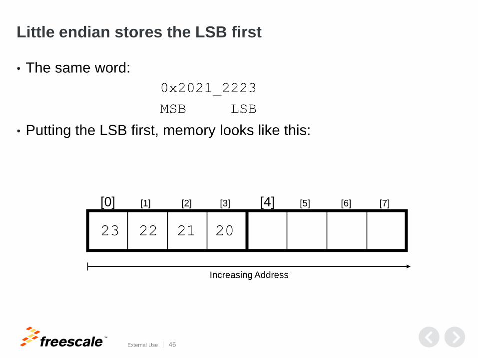
Little endian stores the LSB first
• The same word:
0x2021_2223
MSB LSB
• Putting the LSB first, memory looks like this:
23 22 21 20
[0] [1] [2] [3]
Increasing Address
[4] [5] [6] [7]

TM
External Use 47
Little endian—an alternate view
• To preserve positional order, most prefer to show LE data with the
address increasing from right-to-left
• The same word:
0x2021_2223
MSB LSB
• For LE, putting the LSB at the lowest address, memory looks like
this:
20 21 22 23
[0] [3] [2] [1]
Increasing Address
[4] [7] [6] [5]

TM
External Use 48
20 21 22 23
[0] [1] [2] [3]
23 22 21 20
[0] [1] [2] [3]
Big Endian
Little Endian
MSB
MSB
Offset of 1 needed to get the
second MSB of a big endian
word, given its starting
address
Offset of 2 needed to get the
second MSB of a little-endian
word, given its starting
address
myPointer
myPointer
Endianness changes the offset

TM
External Use 49
Agenda
• Architecture versions
• Registers and instruction sets
• Exception model
• Memory model
• Coprocessors
• Architecture extensions
• ARM ISA

TM
External Use 50
ARM Instruction Set
ARM architecture supports both ARM and Thumb instruction sets
ARM Instruction Set Thumb Instruction Set
32-bit instructions Mix of 16- and 32-bit instructions
Larger, more flexible instruction set Some instructions are less flexible than the ARM equivalent,
but C/C++ code is normally compiled as Thumb instructions
because it provides the best mix of performance and code
density
Supports the ability to make most instructions conditional
via certain defined suffixes
The instructions themselves cannot be made conditional,
but conditions can be added in code via IT instructions
• Instruction types
− Load/Store instructions – for memory access
− Data processing instructions – operate on register content
− Flow control instructions – branching
− Miscellaneous instructions – breakpoint, wait for interrupt/event, no-op
− DSP instructions – SIMD instructions for data packing/unpacking and data processing

TM
External Use 51
Agenda
• ARM V7 ISA Overview
− Load/Store instruction sets
− Data Processing instruction sets
− Flow Control instruction sets
− Coprocessor instructions

TM
External Use 52
Load/Store Instructions
• Multiple Data transfer from / to memory use LDM and STM instructions
• The instruction syntax:
• xxM <type> <cond> < Rb>, {<register list>}
• xx = LD or ST ( load or store )
• IA = increment after ( do the LD or ST then increment )
• IB = increment before ( do the increment then LD or ST)
• DA = decrement after ( do the LD or ST then decrement )
• DB = decrement before ( do the decrement then LD or ST)
• Rb = memory location base register
r5
r3
r1 r8
0x100
r3
r1
r5
r8
0x100 r3
r5
r1 r8
0x100 r1
r3
r5
r8
0x100
STMIA r8, { r1,r3,r5} ; store r8 then increment
STMIB r8, { r1,r3,r5} ; Increment r8 base then store
STMDA r8, { r5,r3,r1} ; store r8 then decrement
STMDB r8, { r5,r3,r1} ;decrement r8 base then store
memory .
.
.
memory .
.
.
memory ,
,
,
memory .
.
.

TM
External Use 53
Agenda
• ARM V7 ISA Overview
− Load/Store instruction sets
− Data Processing instruction sets
− Flow Control instruction sets
− Coprocessor instructions

TM
External Use 54
Data Processing Instructions
Logical Shift Lift Immediate – LSL LSL r3, r4, #5
n is the number of bit positions by which the value is shifted lift.
N = 0…31
x
bit
31
bit
0 Before
bit
30 0 After shift left by 1
bit
0 bit
31
Carry
n “0” bits have been shifted in on the right and the carry is set to bit 32-n of the original word.
Logical Shift Right Immediate – LSR LSR r3, r4, #5
n is the number of bit positions by which the value is shifted right.
N = 0…31
x
bit
31
bit
0 Before
0 bit
1 After shift right by 1
bit
31 bit
0
Carry
n “0” bits have been shifted in on the lift and the carry is set to bit n-1 of the original word.
Shift Operation
TM
External Use 55
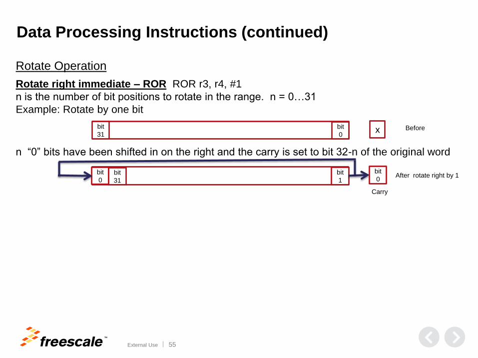
Data Processing Instructions (continued)
Rotate right immediate – ROR ROR r3, r4, #1
n is the number of bit positions to rotate in the range. n = 0…31
Example: Rotate by one bit
x bit
31
bit
0 Before
bit
0
bit
1 After rotate right by 1 bit
31
bit
0
Carry
n “0” bits have been shifted in on the right and the carry is set to bit 32-n of the original word
Rotate Operation

TM
External Use 56
Data Processing Instructions (continued)
Multiply operation
There are two types of multiply operation:
• Normal -32-bit result stores in register
• Long -64-bit result stores in register
Example:
• 32-bit multiplication
• MUL r1, r3, r5 r1 = r3 * r5
Example:
• 64-bit multiplication
• MULL r8, r7, r3, r5 r7:r8 = r3 * r5
• Both types can perform accumulate operation
MUL Mult.
MLA Mult. Accum
MLS Mult. Signed
UMULL Mult. Unsigned Long
UMLAL Mult. Accum Unsigned Long
SMULL Mult. Signed Long
SMLAL Mult. Accum Signed Long

TM
External Use 57
Data Processing Instructions (continued)
• Comparison and Test operation
• The result of comparison or test operation are not stored. These instruction only set the appropriate N,Z, C, and V bits of CPSR
Example:
• Compare
• CMP Rn, Op2 Rn – Op2
• Compare Negative
• CMN Rn, Op2 Rn + Op2
• Bit Test
• TST Rn, Op2 Rn ^ Op2
• Test Equal
• TEQ Rn,Op2 Rn = Op2
Flags
Status Flag Description
N Negative – bit 31 of the result has been set.
Z Zero – result of operation was zero.
C Carry – result was grater than 32 bits.
V Overflow- result was grater than 31 bits.

TM
External Use 58
Condition codes and Flags
• ARM instructions can be made conditional through the
addition of a list of defined condition suffixes
• For example an add instruction:
• ADD r0, r1, r2 ;r0 = r1 + r2
• Now execute the add instruction only is zero flag is
set:
• ADDEQ r0, r1, r2 ;if zero flag is set
;than r0 = r1 + r2
• By default, data processing operations do not affect the
condition. To cause the condition flags to be updated,
the S bit of the instruction needs to be set by appending
the instruction with an S
• For example to add two numbers and set the condition
flags:
• ADDS r0,r1,r2 ;r0 = r1 + r2
;and set flags
Condition codes
Suffix Description
EQ Equal
NE Not equal
CS/HS Unsigned higher or same
CC/LO Unsigned lower
MI Minus
PL Positive or zero
VS Overflow
VC No overflow
HI Unsigned higher
LS Unsigned lower or same
GE Greater than or equal
LT Less than
GR Greater than
LE Less than or equal
AL Always (default)
Flags
Status Flag Description
N Negative – bit 31 of the result has been set.
Z Zero – result of operation was zero.
C Carry – result was grater than 32 bits.
V Overflow- result was grater than 31 bits.

TM
External Use 59
Agenda
• ARM V7 ISA Overview
− Load/Store instruction sets
− Data Processing instruction sets
− Flow Control instruction sets
− Coprocessor instructions

TM
External Use 60
Flow control instructions
Branch Operation
The branch group provides the ability to locate any point in the program with a single operation
Simple branch:
The basic branch instruction is: B{cond} <expression>
<expression> is the address within the program to which you wish to transfer control. Usually, it is just a label
which is defined elsewhere in the program
Branch with link:
The branch with link instruction is: BL{cond} <sub_routine_expression>
The branch with link operation is to perform a link operation before the branch is executed. This
means storing the current value of R15(pc) in R14(lr) before the branch is taken, so that the program
has some way of returning. MOV r15,r14 or MOV pc,lr
Store return address in LR STMFD sp!, {r0,lr} ; push to stack
Return by restoring PC from LR LDMFD sp! ,{r0,pc} ; pop from stack
Main prog. func_1 func_2
:
:
:
BL func_1
:
:
:
:STMFD sp!, {r0,lr}
:
:
BL func_2
:
LDMFD sp!,{r0,pc}
:
:
:
:
:
:
MOV pc,lr

TM
External Use 61
Agenda
• ARM V7 ISA Overview
− Load/Store instruction sets
− Data Processing instruction sets
− Flow Control instruction sets
− Coprocessor instructions

TM
External Use 62
Coprocessor Instructions
• There are 3 types of coprocessor instructions:
− Data processing
− Register transfer
− Memory transfer
Op Code Coprocessor Instructions Description
CDP Data processing Initiate a coprocessor data processing operation
MRC Register transfer Move to ARM register from coprocessor register
MCR Register transfer Move to coprocessor register from ARM register
LDC Memory transfer Load coprocessor register from memory
STC Memory transfer
Store from coprocessor register to memory
TM
External Use 63
Session Summary
This session covered various difference and similarity between
programming model of Power Architecture and ARM Architecture.
The session will provided:
• Architectural versions on both PowerPC and ARM Architecture
• Registers and instruction sets
• Exception model
• Coprocessors
• Architecture Extensions
• ARM ISA

TM
External Use 64
Introducing The
QorIQ LS2 Family
Breakthrough,
software-defined
approach to advance
the world’s new
virtualized networks
New, high-performance architecture built with ease-of-use in mind Groundbreaking, flexible architecture that abstracts hardware complexity and
enables customers to focus their resources on innovation at the application level
Optimized for software-defined networking applications Balanced integration of CPU performance with network I/O and C-programmable
datapath acceleration that is right-sized (power/performance/cost) to deliver
advanced SoC technology for the SDN era
Extending the industry’s broadest portfolio of 64-bit multicore SoCs Built on the ARM® Cortex®-A57 architecture with integrated L2 switch enabling
interconnect and peripherals to provide a complete system-on-chip solution

TM
External Use 65
QorIQ LS2 Family Key Features
Unprecedented performance and
ease of use for smarter, more
capable networks
High performance cores with leading
interconnect and memory bandwidth
• 8x ARM Cortex-A57 cores, 2.0GHz, 4MB L2
cache, w Neon SIMD
• 1MB L3 platform cache w/ECC
• 2x 64b DDR4 up to 2.4GT/s
A high performance datapath designed
with software developers in mind
• New datapath hardware and abstracted
acceleration that is called via standard Linux
objects
• 40 Gbps Packet processing performance with
20Gbps acceleration (crypto, Pattern
Match/RegEx, Data Compression)
• Management complex provides all
init/setup/teardown tasks
Leading network I/O integration
• 8x1/10GbE + 8x1G, MACSec on up to 4x 1/10GbE
• Integrated L2 switching capability for cost savings
• 4 PCIe Gen3 controllers, 1 with SR-IOV support
• 2 x SATA 3.0, 2 x USB 3.0 with PHY
SDN/NFV
Switching
Data
Center
Wireless
Access

TM
External Use 66
See the LS2 Family First in the Tech Lab!
4 new demos built on QorIQ LS2 processors:
Performance Analysis Made Easy
Leave the Packet Processing To Us
Combining Ease of Use with Performance
Tools for Every Step of Your Design

TM
© 2014 Freescale Semiconductor, Inc. | External Use
www.Freescale.com