Embed Size (px)
Citation preview

○Product structure:Silicon monolithic integrated circuit ○This product has no designed protection against radioactive rays
1/25 TSZ22111・14・001
TSZ02201-0T1T0C700150-1-2
09.Dec.2015 Rev.001
www.rohm.com © 2015 ROHM Co., Ltd. All rights reserved.
Constant Current LED Drivers
50V 200mA 1ch Source Driver for Automotive BD8372HFP-M BD8372EFJ-M
General Description BD8372HFP-M and BD8372EFJ-M are LED source drivers capable of withstanding high input voltage (50V MAX). The constant current output is set by either of two external resistors. It has built-in LED open/short protection, external resistance open/short protection and overvoltage protection that can achieve high reliability. It is possible to control all LEDs together and turn OFF even if LED causes short/open in a certain row when driving two or more LEDs by using multiple ICs.
Features Variable form Constant- Current Source H/L Current Setting Switch Control LED Open/Short Protection Circuit Integrated ISET Open/Short Protection Circuit Integrated Overvoltage Mute and Temperature Protection
Function Integrated Abnormal Output Detection and Output Functions
(PBUS)
Applications For automotive (Rear lamp, Interior light, etc.).
Basic Application Circuit
Key Specifications
Input Voltage Range: 5.5V to 40V Max Output Current: 200mA(MAX) Output Current Accuracy: ±8%(Max) Operating Temperature Range: -40°C to +125°C
Packages W (Typ) x D (Typ) x H (Max)
HRP7 9.395mm x 10.540mm x 2.005mm HTSOP-J8 4.90mm x 6.00mm x 1.00mm
HRP7
HTSOP-J8
BD8372HFP-M
BD8372EFJ-M
VIN
STOP
ISETHISETL
PBUS GND
FIN
IOUT
Figure 1. Typical Application Circuit
Datasheet
Datasheet

2/25
BD8372HFP-M BD8372EFJ-M
© 2015 ROHM Co., Ltd. All rights reserved. www.rohm.com
TSZ22111・15・001 09.Dec.2015 Rev.001
TSZ02201-0T1T0C700150-1-2
Pin Configurations
Figure 2. HRP7 Package Pin Configuration Figure 3. HTSOP-J8 Package Pin Configuration
Pin Descriptions
HRP7 HTSOP-J8
Pin No. Pin Name Description Pin No. Pin Name Description
1 STOP Input terminal for Brake lamp 1 VIN Power supply input
2 PBUS Error detection I/O terminal 2 IOUT Current output terminal
3 ISETL Current setting terminal (L mode) 3 GND GND
4 GND GND 4 GND GND
5 ISETH Current setting terminal (H mode) 5 STOP Input terminal for Brake lamp
6 VIN Power supply input 6 PBUS Error detection I/O terminal
7 IOUT Current output terminal 7 ISETL Current setting terminal (L mode)
8 ISETH Current setting terminal (H mode)
HRP7 (TOP VIEW)
HTSOP-J8 (TOP VIEW)
1 2 3 4
8 7 6 5

3/25
BD8372HFP-M BD8372EFJ-M
© 2015 ROHM Co., Ltd. All rights reserved. www.rohm.com
TSZ22111・15・001 09.Dec.2015 Rev.001
TSZ02201-0T1T0C700150-1-2
Block Diagram
VREF
VIN
STOP
Current
CONTROL
VIN
VIN-0.2V
VREF
VREF
PBUS
led off
H/L MODE
SET
Iref_l Iref_h
Iref_l Iref_h
PROTECTled open
mode
LED OPEN
DET
led short
0.8V0.8V GND
IOUT
ISETL ISETH
0.6V
Figure 4. Block Diagram

4/25
BD8372HFP-M BD8372EFJ-M
© 2015 ROHM Co., Ltd. All rights reserved. www.rohm.com
TSZ22111・15・001 09.Dec.2015 Rev.001
TSZ02201-0T1T0C700150-1-2
Absolute Maximum Ratings (Ta=25°C)
Parameter Symbol Rating Unit
Power Supply Voltage VIN -0.3 to +50 V
STOP, IOUT, PBUS Terminal VSTOP, VIOUT, VPBUS -0.3 to VIN+0.3 V
ISETH, ISETL Terminal VISETH, VISETL -0.3 to +7 V
Power Consumption Pd
HRP7 2.3 (Note 1)
W
HTSOP-J8 1.1 (Note 2)
Operating Temperature Range Topr -40 to +125 °C
Storage Temperature Range Tstg -55 to +150 °C
Junction Temperature Tjmax 150 °C
IOUT Output Maximum Current IIOUT 200 mA
(Note 1) HRP7 IC mounted on glass epoxy 2-layer board area 15mmx15mm of the back copper foil, measuring 70mmx70mmx1.6mm. Pd decreased at 18.4mw/°C for temperatures above Ta=25°C.
(Note 2) HTSOP-J8 IC mounted on glass epoxy 2-layer board area 15mmx15mm of the back copper foil, measuring 70mmx70mmx1.6mm. Pd decreased at 8.8mW/°C for temperatures above Ta=25°C. Caution: Operating the IC over the absolute maximum ratings may damage the IC. The damage can either be a short circuit between pins or an open circuit between pins and the internal circuitry. Therefore, it is important to consider circuit protection measures, such as adding a fuse, in case the IC is operated over the absolute maximum ratings.
Recommended Operating Conditions (Ta=-40°C to +125°C) (Please set after considering power consumption for the power-supply voltage.)
Parameter Symbol
Rating
Unit Conditions
Min Typ Max
Power Supply Voltage VIN 5.5 13 40 V -
Current Setting Resistor
RISETH 10 - 100 kΩ STOP=H
RISETL 10 - 100 kΩ STOP=L
Minimum Capacitor connecting IOUT terminal
CIOUT 0.1 - - μF

5/25
BD8372HFP-M BD8372EFJ-M
© 2015 ROHM Co., Ltd. All rights reserved. www.rohm.com
TSZ22111・15・001 09.Dec.2015 Rev.001
TSZ02201-0T1T0C700150-1-2
Electrical Characteristics (Unless otherwise specified, Ta=-40°C to 125°C, VIN=13V, RISETL=RISETH=40kΩ, RPBUS=10kΩ)
Parameter Symbol
Limit
Unit Conditions
Min Typ Max
Circuit Current IIN - 2.9 5 mA
IOUT Output Current H IOUT_H
48.5 50 51.5 mA 50mA setting (ISET=40kΩ) STOP=High, Ta=25°C
46 50 54 mA 50mA setting (ISET=40kΩ) STOP=High, Ta=-40°C to +125°C
IOUT Output Current L IOUT_L
4.85 5 5.15 mA 5mA setting (ISET=40kΩ) STOP=Low, Ta=25°C
4.6 5 5.4 mA 5mA setting (ISET=40kΩ) STOP=Low, Ta=-40°C to +125°C
IOUT Drop Voltage H VDRH_IOUT - 0.7 1.2 V 200mA setting(ISET=10kΩ) STOP=High
IOUT Drop Voltage L VDRL_IOUT - 0.5 0.7 V 20mA setting(ISET=10kΩ) STOP=Low
IOUT OFF Current IIOUT_OFF - - 1 µA VIOUT=2V, PBUS=L, Ta=25°C
IOUT Current at GND Short IIOUT_SHORT - - 40 µA VIOUT=0V
ISET Terminal Voltage VISET - 0.8 - V At ISETL or ISETH pins
ISET Short Detection Resistor RISET_SHORT - 5.1k 7.5k Ω At ISETL or ISETH pins
ISET Open Detection Resistor RISET_OPEN 125k 400k - Ω At ISETL or ISETH pins
IOUT LED OPEN Detection VIOUT_OPEN VIN-0.3 VIN-0.2 VIN-0.1 V
IOUT LED Short Detection VIOUT_SHORT 0.2 0.6 1.0 V
STOP Input Voltage H VIH_STOP 4.0 - VIN+0.2 V
STOP Input Voltage L VIL_STOP GND - 1.0 V
STOP Input Current VIN_STOP - 40 100 µA VSTOP=13V
PBUS Input Voltage H VIH_PBUS 4.0 - VIN+0.2 V
PBUS Input Voltage L VIL_PBUS GND - 2.0 V
PBUS Low Voltage VOL_PBUS - - 1.5 V IPBUS=20mA
PBUS Input Current IIN_PBUS - 38 100 µA VPBUS=13V
IN Under Voltage Open Detection Mask Voltage
VUVLO_IOPEN 7.5 8.0 8.5 V
IN Over Voltage Mute Current VIN_OVPMUTE 16 19 24 V 200mA setting (ISET=10kΩ) STOP=High

6/25
BD8372HFP-M BD8372EFJ-M
© 2015 ROHM Co., Ltd. All rights reserved. www.rohm.com
TSZ22111・15・001 09.Dec.2015 Rev.001
TSZ02201-0T1T0C700150-1-2
Typical Performance Curves (Reference Data)
(Unless otherwise specified Ta=25°C, VIN=13V)
Figure 5. IOUT vs RISETL (STOP=Low)
Figure 6. IOUT vs RISETH (STOP=High)
Figure 7. IOUT vs VIN (STOP=Low)
Figure 8. IOUT vs VIN (STOP=High)
VIOUT=3V
RISETH=10kΩ
RISETH=20kΩ
RISETH=40kΩ
VIOUT=3V
RISETL=10kΩ
RISETL=20kΩ
RISETL=40kΩ
7/25
BD8372HFP-M BD8372EFJ-M
© 2015 ROHM Co., Ltd. All rights reserved. www.rohm.com
TSZ22111・15・001 09.Dec.2015 Rev.001
TSZ02201-0T1T0C700150-1-2
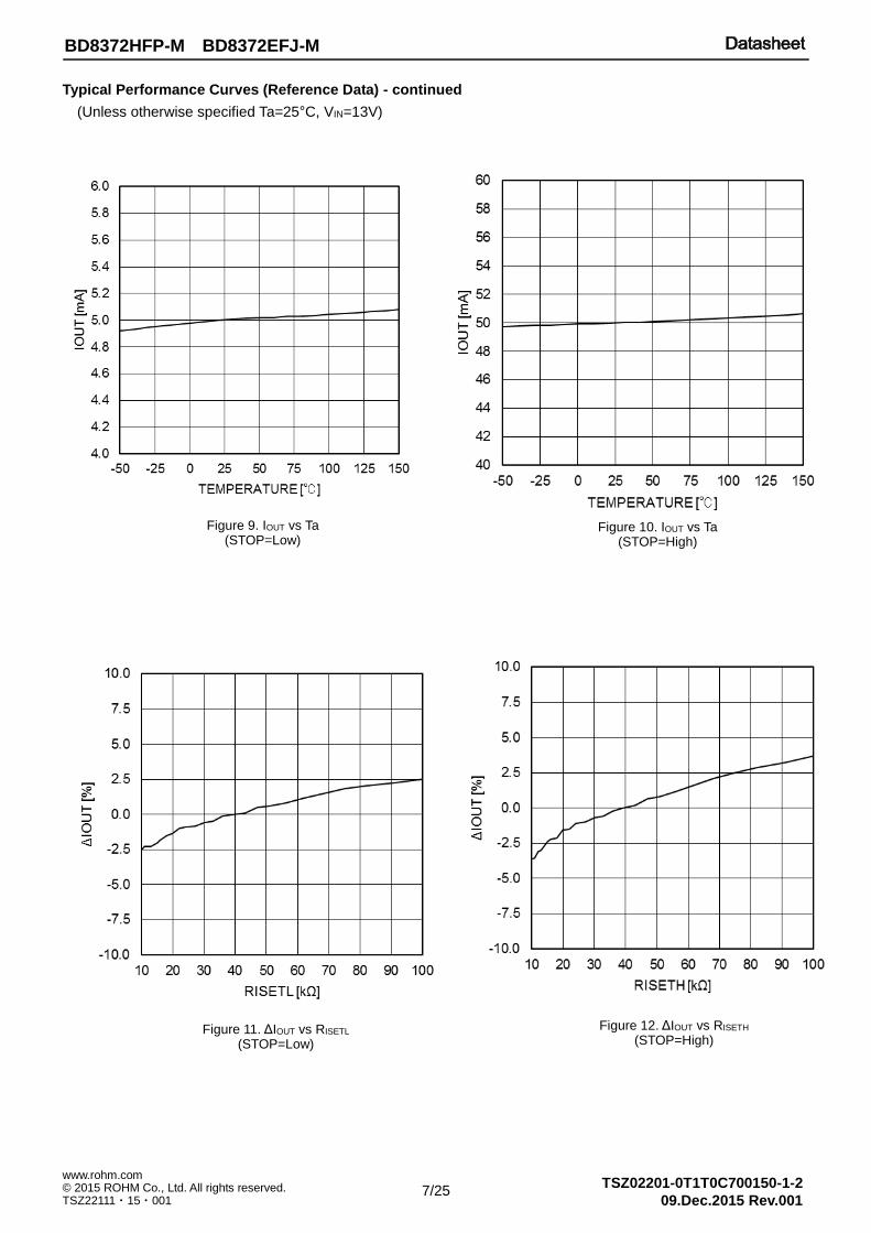
Typical Performance Curves (Reference Data) - continued
(Unless otherwise specified Ta=25°C, VIN=13V)
Figure 9. IOUT vs Ta (STOP=Low)
Figure 10. IOUT vs Ta (STOP=High)
Figure 11. ΔIOUT vs RISETL (STOP=Low)
Figure 12. ΔIOUT vs RISETH (STOP=High)

8/25
BD8372HFP-M BD8372EFJ-M
© 2015 ROHM Co., Ltd. All rights reserved. www.rohm.com
TSZ22111・15・001 09.Dec.2015 Rev.001
TSZ02201-0T1T0C700150-1-2
Timing Chart
VIN
STOP
IOUT
PBUS
Current
Control
H/Lmode
Switch
LEDSHORT
LEDOPEN
VIN
STOP
PBUS
ISETL ISETH
LED SHORT
VIN
LED OPEN
STOP
VIOUT
ISETL
IIOUTH
IIOUTL
VIH_STOPVIL_STOP
ISETH
PBUS
IIOUTL
VIN
VIOUT
ISETL
ISETH
IIOUTH
VIH_STOP
VIL_STOP
Figure 13. Timing Chart
9/25
BD8372HFP-M BD8372EFJ-M
© 2015 ROHM Co., Ltd. All rights reserved. www.rohm.com
TSZ22111・15・001 09.Dec.2015 Rev.001
TSZ02201-0T1T0C700150-1-2
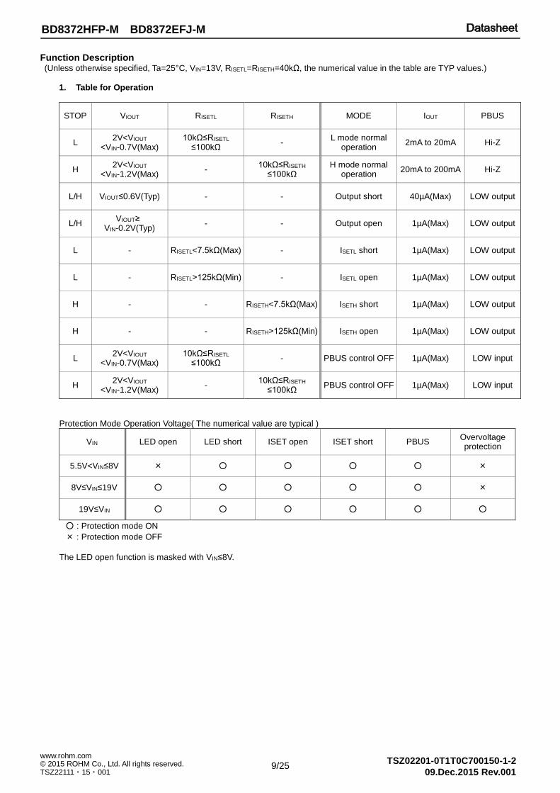
Function Description (Unless otherwise specified, Ta=25°C, VIN=13V, RISETL=RISETH=40kΩ, the numerical value in the table are TYP values.)
1. Table for Operation
STOP VIOUT RISETL RISETH MODE IOUT PBUS
L 2V<VIOUT
<VIN-0.7V(Max) 10kΩ≤RISETL
≤100kΩ -
L mode normal operation
2mA to 20mA Hi-Z
H 2V<VIOUT
<VIN-1.2V(Max) -
10kΩ≤RISETH
≤100kΩ H mode normal
operation 20mA to 200mA Hi-Z
L/H VIOUT≤0.6V(Typ) - - Output short 40µA(Max) LOW output
L/H VIOUT≥
VIN-0.2V(Typ) - - Output open 1µA(Max) LOW output
L - RISETL<7.5kΩ(Max) - ISETL short 1µA(Max) LOW output
L - RISETL>125kΩ(Min) - ISETL open 1µA(Max) LOW output
H - - RISETH<7.5kΩ(Max) ISETH short 1µA(Max) LOW output
H - - RISETH>125kΩ(Min) ISETH open 1µA(Max) LOW output
L 2V<VIOUT
<VIN-0.7V(Max) 10kΩ≤RISETL
≤100kΩ - PBUS control OFF 1µA(Max) LOW input
H 2V<VIOUT
<VIN-1.2V(Max) -
10kΩ≤RISETH
≤100kΩ PBUS control OFF 1µA(Max) LOW input
Protection Mode Operation Voltage( The numerical value are typical )
VIN LED open LED short ISET open ISET short PBUS Overvoltage protection
5.5V<VIN≤8V × ○ ○ ○ ○ ×
8V≤VIN≤19V ○ ○ ○ ○ ○ ×
19V≤VIN ○ ○ ○ ○ ○ ○
○ : Protection mode ON
× : Protection mode OFF
The LED open function is masked with VIN≤8V.

10/25
BD8372HFP-M BD8372EFJ-M
© 2015 ROHM Co., Ltd. All rights reserved. www.rohm.com
TSZ22111・15・001 09.Dec.2015 Rev.001
TSZ02201-0T1T0C700150-1-2
2. Method of Setting Current
The IC regulates the voltage at ISETL/ISETH to VISET (0.8V typ) across the external resistor to set IOUT. Then IOUT is set by setting STOP High or Low.
VIN
STOP
IOUT
PBUS
+B
LED
OPEN
Current
Control
H/Lmode
Switch
0.8V(typ)
GND
Iref_lIref_l
ISETL ISETH
0.8V(typ)
RISETL RISETH
Figure 14. Current setting method
L mode (STOP=Low) H mode (STOP=High)
exp) exp)
AR
VI
ISETLIOUT 250
8.0
mAk
VIkR OUTIISETL 5250
40
8.06.1
AR
VI
ISETHIOUT 2500
8.0
mAk
VIkR OUTIISETH 502500
40
8.040
IOUT Output current VS ISET connect resistance
0.0010
0.0100
0.1000
1.0000
1.00E+03 1.00E+04 1.00E+05 1.00E+06
RISET[Ω ]
IOU
T[A
]
H mode
L mode
R_ISET setting range
short protection open protection
RISET[Ω]
I OU
T[A
]
IOUT Output Current vs ISET Connect Resistance
11/25
BD8372HFP-M BD8372EFJ-M
© 2015 ROHM Co., Ltd. All rights reserved. www.rohm.com
TSZ22111・15・001 09.Dec.2015 Rev.001
TSZ02201-0T1T0C700150-1-2
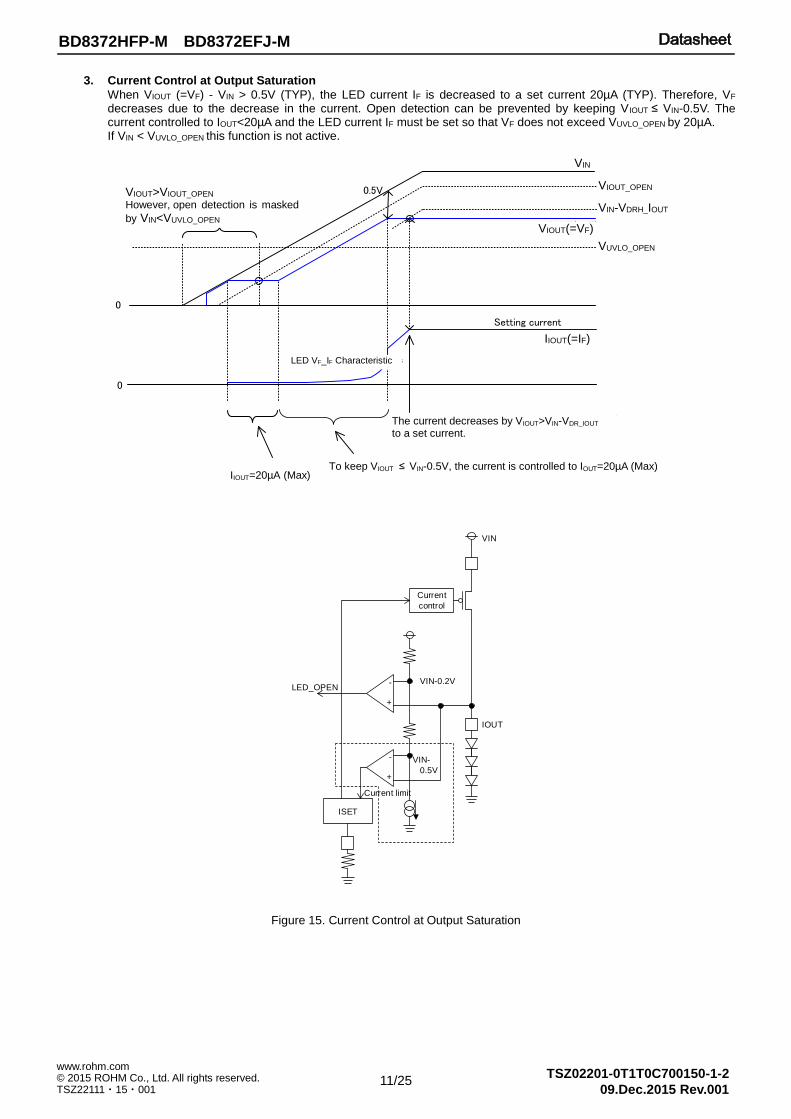
3. Current Control at Output Saturation
When VIOUT (=VF) - VIN > 0.5V (TYP), the LED current IF is decreased to a set current 20µA (TYP). Therefore, VF decreases due to the decrease in the current. Open detection can be prevented by keeping VIOUT ≤ VIN-0.5V. The current controlled to IOUT<20µA and the LED current IF must be set so that VF does not exceed VUVLO_OPEN by 20µA. If VIN < VUVLO_OPEN this function is not active.
VIOUT(=VF)
VIOUT_OPEN
VUVLO_OPEN
VIN
IIOUT(=IF)
LED VF_IF Characteristic
IOUT=20uA(max)To keep VIOUT≦VIN-0.4V, the current is controlled. ※To IOUT=20uA(max)
VIOUT>VIOUT_OPENHowever, open detection is masked by VIN<VUVLO_OPEN.
Setting current
0
0
VIN-VDRH_IOUT
0.5V
The current decreases by VIOUT>VIN-VDR_IOUT for a set current.
Current
control
+
-
+
-
ISET
Current limit
VIN-0.2V
VIN-
0.5V
LED_OPEN
IOUT
VIN
Figure 15. Current Control at Output Saturation
VIOUT>VIOUT_OPEN VIOUT>VIOUT_OPEN
However, open detection is masked
by VIN<VUVLO_OPEN
VIN
VIOUT_OPEN
VIN-VDRH_IOUT
VIOUT(=VF)
VUVLO_OPEN
IIOUT(=IF)
To keep VIOUT ≤ VIN-0.5V, the current is controlled to IOUT=20µA (Max) IIOUT=20µA (Max)
The current decreases by VIOUT>VIN-VDR_IOUT
to a set current.
LED VF_IF Characteristic

12/25
BD8372HFP-M BD8372EFJ-M
© 2015 ROHM Co., Ltd. All rights reserved. www.rohm.com
TSZ22111・15・001 09.Dec.2015 Rev.001
TSZ02201-0T1T0C700150-1-2
4. PROTECT BUS (PBUS) PBUS is an I/O terminal that outputs any detected error by switching PBUS from Hi-Z (Note 1) to Low. The output current can also be turned OFF by pulling the PBUS Low. When driving multiple LEDs through multiple ICs, as shown in the figure below, all the rows of LEDs can be turned OFF by any fault by connecting PBUS terminal to each IC. (Note1) PBUS terminal is an open drain terminal. Even when used separately, please be pulled up(10kΩ) to power supply voltage.
VIN IOUT
PBUS=Hi-Z ⇒ LOW
LEDOPENSTOP
PBUS
ISE
TL
ISE
TH
GN
D
+B
IOUTVIN
STOP
PBUS
ISE
TL
ISE
TH
GN
D
LEDOFF
IOUTVIN
STOP
PBUS
ISE
TL
ISE
TH
GN
D
LEDOFF
PROTECT BUS
Figure 16. PBUS Function
● Example of operating protection for an LED open condition
VIOUT
PBUS
CH2
CH3
VIOUT_SHORT
VIOUT-OPEN
VIOUT
IIOUT
VIOUT
IIOUT
clamps to 1.4V
LED Open
IIOUTCH1
LOWHi-Z Hi-Z
0
0
VIOUT_SHORT
0
0
0
0
Figure 17. Example of protective Operation When LED becomes open on the first IC, PBUS of IC1 is switched from Hi-Z to Low. As PBUS becomes Low, the other ICs detect the error and turns OFF their own LEDs. VIOUT clamps to 1.4V during the OFF period in order to prevent ground short protection.
VIOUT_OPEN
VIOUT_SHORT
VIOUT_SHORT
IIOUT
VIOUT
IIOUT
VIOUT
VIOUT
IIOUT

13/25
BD8372HFP-M BD8372EFJ-M
© 2015 ROHM Co., Ltd. All rights reserved. www.rohm.com
TSZ22111・15・001 09.Dec.2015 Rev.001
TSZ02201-0T1T0C700150-1-2
5. Protection Function This IC has built-in short/open protection function for the external components. Any error detected will pull the PBUS terminal low.
Figure 18. LED Open detection function
CurrentControl
0.6V
PBUS
VIN IOUT
Short
OFF+B
OFF control
Figure 19. LED Short detection function
CurrentControl
4.3V
PBUS
VIN IOUT
OFF+B
ISET
×
Figure 20. ISET Pin open detection function
CurrentControl
PBUS
VIN IOUT
OFF+B
ISET
0.05V
Figure 21. ISET Pin short detection function
CurrentControl
VIN-0.2VPBUS
VIN IOUT
×
OFFする+B
オープン
Open
(1) LED Open Detecting Function When any LED connected at the IOUT becomes open, VIOUT will go HIGH. When an error is detected at VIOUT < VIOUT_OPEN the PBUS is pulled LOW.
(2) LED Short Detecting Function When the LEDs connected at the IOUT terminal are shorted to ground, VIOUT will go LOW. When an error is detected at VIOUT < VIOUT_SHORT 0.6V (TYP) the output current is turned OFF to prevent IC heating and the PBUS is pulled LOW.
(3) ISET(H/L) Open Detecting Function When the external resistance connected at ISETL or ISETH terminal > RISET_OPEN 400k (TYP), the output current is turned OFF to prevent IC heating and the PBUS is pulled LOW. This detection is not affected by the current setting mode.
(4) ISET(H/L) Short Detecting Function
When the external resistance connected at ISETL or ISETH terminal < RISET_SHORT 5.1k (TYP), the output current is turned OFF to protect the LEDs and the PBUS is pulled LOW. This detection is not affected by the current setting mode.

14/25
BD8372HFP-M BD8372EFJ-M
© 2015 ROHM Co., Ltd. All rights reserved. www.rohm.com
TSZ22111・15・001 09.Dec.2015 Rev.001
TSZ02201-0T1T0C700150-1-2
6. Over Voltage Protection
Overvoltage protection works in (RISETH=40kΩ), 18V (TYP) ≤ VIN at IOUT=200mA setting and limits output current to suppress the upswing in heat generation of LSI. The overvoltage mute protection is effective only for (STOP=High) at H mode time.
200mA
10mA
Iomax
VIN19V0V 13V 40V24V
電源過電圧による
出力電流ミュート
Figure 22. Overvoltage mute function
Over Voltage Protection Current Limit
IOMAX

15/25
BD8372HFP-M BD8372EFJ-M
© 2015 ROHM Co., Ltd. All rights reserved. www.rohm.com
TSZ22111・15・001 09.Dec.2015 Rev.001
TSZ02201-0T1T0C700150-1-2
Recommended application circuit
BD8372
+B
TAILD1
D2
D3
STOP
FL1
2.5kΩ@100MHz
10k0.1μF 10k
ZD1 4.7μF
10k
STOP
PBUS
ISETL
39k
ISETH
39k
GND
VIN
IOUT
0.1μF
Figure 23. Recommended application circuit
(Note) EMC ISO 11452-2 (ALSE) ISO 11452-4 (BCI) ISO 7637-2
・ pulse1
・ Pulse2a,2b (level4)
・ Pulse3a,3b (level4)
No.
Component Name
Component Value
Product Name
Company
1 D1 - RF201L2S ROHM
2 D2 - RF201L2S ROHM
3 D3 - RF201L2S ROHM
4 ZD1 - TNR12H-220K NIPPON CHEMICON
5 FL1 - HMZ2012R102A TDK
6 CVIN 4.7µF GCM32ER71H475KA40 murata
7 CIOUT 0.1µF GCM188R11H104KA42 murata
8 CSTOP 0.1µF GCM188R11H104KA42 murata
9 RISETL 39kΩ MCR03 Series ROHM
10 RISETH 39kΩ MCR03 Series ROHM
11 RPBUS 10kΩ MCR03 Series ROHM
12 R1 10kΩ MCR03 Series ROHM
13 R2 10kΩ MCR03 Series ROHM
Table 1. BOM List

16/25
BD8372HFP-M BD8372EFJ-M
© 2015 ROHM Co., Ltd. All rights reserved. www.rohm.com
TSZ22111・15・001 09.Dec.2015 Rev.001
TSZ02201-0T1T0C700150-1-2
Power Dissipation HRP7 Package HTSOP-J8 Package (Caution1) When mounted with 70.0mm x 70.0mm x 1.6mm glass epoxy substrate. (Caution2) Abobe copper foil area indicates backside copper foil area. (Caution3) Value changes according to number of substrate layers and copper foil area.Note that this value is a measured value. Not a guaranteed value.
Figure 24. Thermal Dissipation Curve
5.0
0.0
4.0
0 25 50 75 100 125 150
Temp Ta [℃]
Po
wer
dis
sip
atio
n P
d [
W]
4.16W
2 layer copper foil 50mm x 50mm
θ ja = 30℃/W
3.0
2.0
1.0
2.3W
1.6W
2 layer copper foil 15mm x 15mm
θ ja = 54.4℃/W
1 layer
θ ja = 78.1℃/W
2.0
0.00 25 50 75 100 125 150
Temp Ta [℃]
Po
wer
dis
sip
atio
n P
d [
W]
1.0
2 layer copper foil 50mm x 50mm
θ ja = 69℃/W
2 layer copper foil 15mm x 15mm
θ ja = 113.6℃/W
1 layer
θ ja = 153.2℃/W
0.82W
1.1W
1.81W
17/25
BD8372HFP-M BD8372EFJ-M
© 2015 ROHM Co., Ltd. All rights reserved. www.rohm.com
TSZ22111・15・001 09.Dec.2015 Rev.001
TSZ02201-0T1T0C700150-1-2
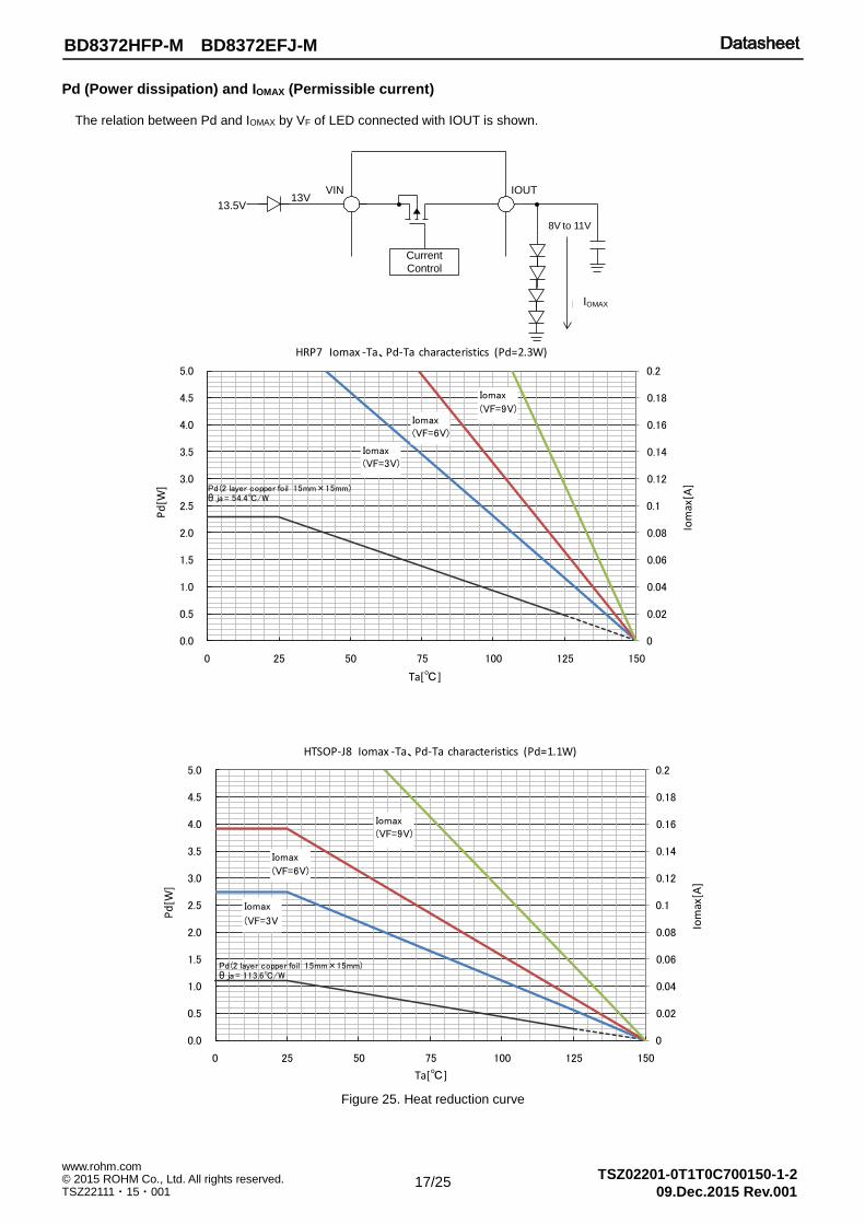
Pd (Power dissipation) and IOMAX (Permissible current) The relation between Pd and IOMAX by VF of LED connected with IOUT is shown.
Figure 25. Heat reduction curve
HRP7
0
0.02
0.04
0.06
0.08
0.1
0.12
0.14
0.16
0.18
0.2
0.0
0.5
1.0
1.5
2.0
2.5
3.0
3.5
4.0
4.5
5.0
0 25 50 75 100 125 150
HRP7 Iomax -Ta、Pd-Ta characteristics (Pd=2.3W)
Pd
[W]
Iom
ax[A
]Pd (2 layer copper foil 15mm×15mm)θ ja = 54.4℃/W
Iomax(VF=6V)
Iomax (VF=3V)
Iomax
(VF=9V)
Ta[℃]
0
0.02
0.04
0.06
0.08
0.1
0.12
0.14
0.16
0.18
0.2
0.0
0.5
1.0
1.5
2.0
2.5
3.0
3.5
4.0
4.5
5.0
0 25 50 75 100 125 150
HTSOP-J8 Iomax -Ta、Pd-Ta characteristics (Pd=1.1W)
Pd
[W]
Iom
ax[A
]
Pd (2 layer copper foil 15mm×15mm)θ ja = 113.6℃/W
Iomax
(VF=6V)
Iomax
(VF=3V
Iomax(VF=9V)
Ta[℃]
VIN IOUT
8V~11V
Iomax
13.5V
Current
Control
13V
IOMAX
8V to 11V

18/25
BD8372HFP-M BD8372EFJ-M
© 2015 ROHM Co., Ltd. All rights reserved. www.rohm.com
TSZ22111・15・001 09.Dec.2015 Rev.001
TSZ02201-0T1T0C700150-1-2
I/O Equivalent Circuit
Pin No. Pin Name I/O Equivalent Circuit
1 STOP
2 PBUS
3 ISETL
4 GND -
300kΩ
VIN
(6pin)
GND
(4pin)
STOP
(1pin)
100kΩ
5V
VIN
(6pin)
GND
(4pin)
PBUS
(28pin)
5V
200kΩ
5V
VIN
(6pin)
GND
(4pin)
ISETL
(3pin)
5V
5V

19/25
BD8372HFP-M BD8372EFJ-M
© 2015 ROHM Co., Ltd. All rights reserved. www.rohm.com
TSZ22111・15・001 09.Dec.2015 Rev.001
TSZ02201-0T1T0C700150-1-2
I/O Equivalent Circuit – continued
Pin No. Pin Name I/O Equivalent Circuit
5 ISETH
6 VIN -
7 IOUT
VIN
(6pin)
GND
(4pin)
ISETH
(5pin)
5V
5V
VIN
(6pin)
GND
(4pin)
IOUT
(7pin)
5V

20/25
BD8372HFP-M BD8372EFJ-M
© 2015 ROHM Co., Ltd. All rights reserved. www.rohm.com
TSZ22111・15・001 09.Dec.2015 Rev.001
TSZ02201-0T1T0C700150-1-2
Operational Notes
1. Reverse Connection of Power Supply
Connecting the power supply in reverse polarity can damage the IC. Take precautions against reverse polarity when connecting the power supply, such as mounting an external diode between the power supply and the IC’s power supply pins.
2. Power Supply Lines
Design the PCB layout pattern to provide low impedance supply lines. Separate the ground and supply lines of the digital and analog blocks to prevent noise in the ground and supply lines of the digital block from affecting the analog block. Furthermore, connect a capacitor to ground at all power supply pins. Consider the effect of temperature and aging on the capacitance value when using electrolytic capacitors.
3. Ground Voltage
Ensure that no pins are at a voltage below that of the ground pin at any time, even during transient condition.
4. Ground Wiring Pattern
When using both small-signal and large-current ground traces, the two ground traces should be routed separately but connected to a single ground at the reference point of the application board to avoid fluctuations in the small-signal ground caused by large currents. Also ensure that the ground traces of external components do not cause variations on the ground voltage. The ground lines must be as short and thick as possible to reduce line impedance.
5. Thermal Consideration
Should by any chance the power dissipation rating be exceeded the rise in temperature of the chip may result in deterioration of the properties of the chip. In case of exceeding this absolute maximum rating, increase the board size and copper area to prevent exceeding the Pd rating.
6. Recommended Operating Conditions
These conditions represent a range within which the expected characteristics of the IC can be approximately obtained. The electrical characteristics are guaranteed under the conditions of each parameter.
7. Inrush Current
When power is first supplied to the IC, it is possible that the internal logic may be unstable and inrush current may flow instantaneously due to the internal powering sequence and delays, especially if the IC has more than one power supply. Therefore, give special consideration to power coupling capacitance, power wiring, width of ground wiring, and routing of connections.
8. Operation Under Strong Electromagnetic Field
Operating the IC in the presence of a strong electromagnetic field may cause the IC to malfunction.
9. Testing on Application Boards
When testing the IC on an application board, connecting a capacitor directly to a low-impedance output pin may subject the IC to stress. Always discharge capacitors completely after each process or step. The IC’s power supply should always be turned off completely before connecting or removing it from the test setup during the inspection process. To prevent damage from static discharge, ground the IC during assembly and use similar precautions during transport and storage.
10. Inter-pin Short and Mounting Errors
Ensure that the direction and position are correct when mounting the IC on the PCB. Incorrect mounting may result in damaging the IC. Avoid nearby pins being shorted to each other especially to ground, power supply and output pin. Inter-pin shorts could be due to many reasons such as metal particles, water droplets (in very humid environment) and unintentional solder bridge deposited in between pins during assembly to name a few.

21/25
BD8372HFP-M BD8372EFJ-M
© 2015 ROHM Co., Ltd. All rights reserved. www.rohm.com
TSZ22111・15・001 09.Dec.2015 Rev.001
TSZ02201-0T1T0C700150-1-2
Operational Notes – continued
11. Unused Input Pins
Input pins of an IC are often connected to the gate of a MOS transistor. The gate has extremely high impedance and extremely low capacitance. If left unconnected, the electric field from the outside can easily charge it. The small charge acquired in this way is enough to produce a significant effect on the conduction through the transistor and cause unexpected operation of the IC. So unless otherwise specified, unused input pins should be connected to the power supply or ground line.
12. Regarding the Input Pin of the IC
This monolithic IC contains P+ isolation and P substrate layers between adjacent elements in order to keep them isolated. P-N junctions are formed at the intersection of the P layers with the N layers of other elements, creating a parasitic diode or transistor. For example (refer to figure below):
When GND > Pin A and GND > Pin B, the P-N junction operates as a parasitic diode. When GND > Pin B, the P-N junction operates as a parasitic transistor.
Parasitic diodes inevitably occur in the structure of the IC. The operation of parasitic diodes can result in mutual interference among circuits, operational faults, or physical damage. Therefore, conditions that cause these diodes to operate, such as applying a voltage lower than the GND voltage to an input pin (and thus to the P substrate) should be avoided.
Figure 26. Example of monolithic IC structure
13. Thermal Shutdown Circuit(TSD)
This IC has a built-in thermal shutdown circuit that prevents heat damage to the IC. Normal operation should always be within the IC’s power dissipation rating. If however the rating is exceeded for a continued period, the junction temperature (Tj) will rise which will activate the TSD circuit that will turn OFF all output pins. When the Tj falls below the TSD threshold, the circuits are automatically restored to normal operation. Note that the TSD circuit operates in a situation that exceeds the absolute maximum ratings and therefore, under no circumstances, should the TSD circuit be used in a set design or for any purpose other than protecting the IC from heat damage.
14. Sudden Voltage Surge on VIN
Because MOSFETs are used in the output, a very steep change in the VCC voltage may cause the transistors to conduct large current. Take this condition into account when selecting the value of external circuit constants for a certain application.
N NP
+ P
N NP
+
P Substrate
GND
NP
+
N NP
+N P
P Substrate
GND GND
Parasitic
Elements
Pin A
Pin A
Pin B Pin B
B C
E
Parasitic
Elements
GNDParasitic
Elements
CB
E
Transistor (NPN)Resistor
N Region
close-by
Parasitic
Elements

22/25
BD8372HFP-M BD8372EFJ-M
© 2015 ROHM Co., Ltd. All rights reserved. www.rohm.com
TSZ22111・15・001 09.Dec.2015 Rev.001
TSZ02201-0T1T0C700150-1-2
Ordering Information
B D 8 3 7 2 H F P - M T R
Form name Package HFP : HRP7
Packaging and forming specification TR: Embossed tape and reel
(HRP7)
B D 8 3 7 2 E F J - M E 2
Form name Package EFJ : HTSOP-J8
Packaging and forming specification E2: Embossed tape and reel
(HTSOP-J8)
Marking Diagrams
Part Number Marking Package Part Number
BD8372HFP HRP7 Reel of 2000 BD8372HFP-MTR
BD8372 HTSOP-J8 Reel of 2500 BD8372EFJ-ME2
HTSOP-J8(TOP VIEW)
B D 8 3 7 2
Part Number Marking
LOT Number
1PIN MARK
HRP7 (TOP VIEW)
BD8372HFP
Part Number Marking
LOT Number
1PIN MARK
23/25
BD8372HFP-M BD8372EFJ-M
© 2015 ROHM Co., Ltd. All rights reserved. www.rohm.com
TSZ22111・15・001 09.Dec.2015 Rev.001
TSZ02201-0T1T0C700150-1-2
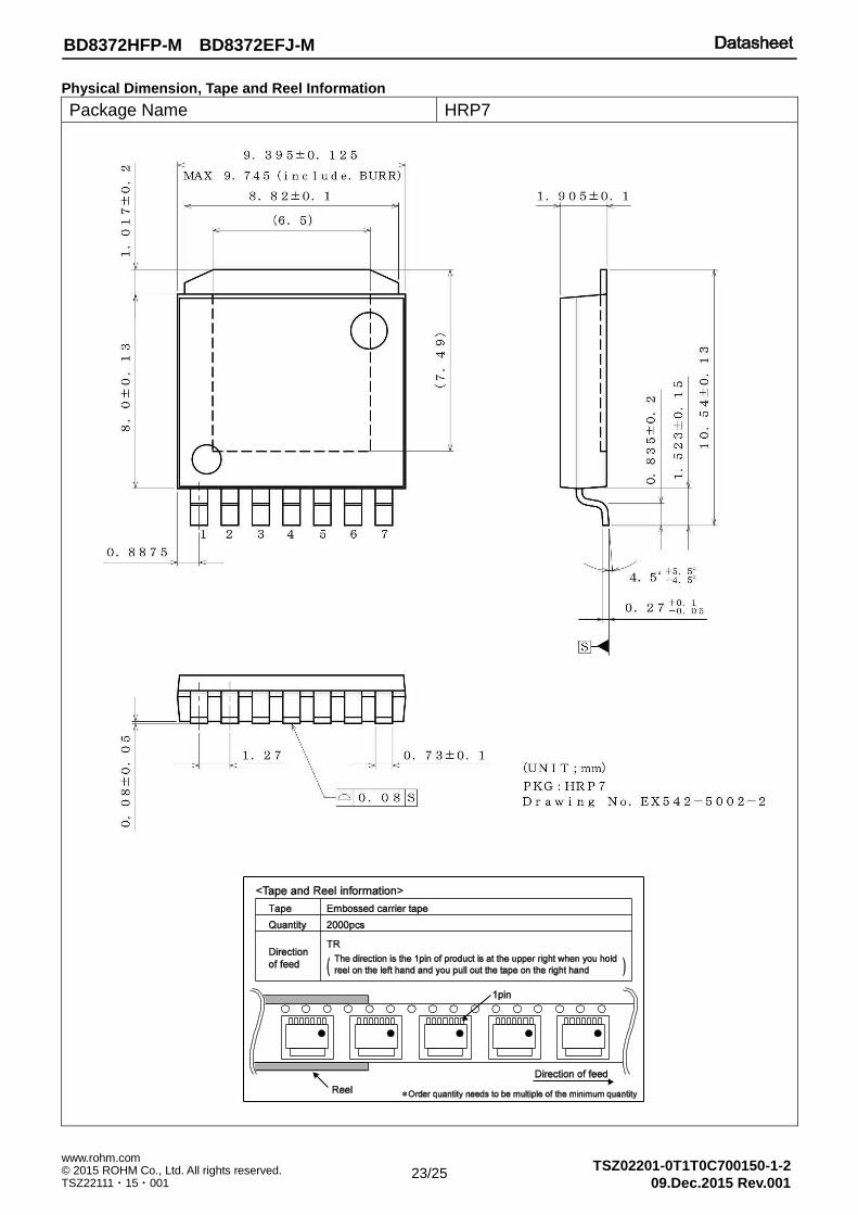
Physical Dimension, Tape and Reel Information
Package Name HRP7

24/25
BD8372HFP-M BD8372EFJ-M
© 2015 ROHM Co., Ltd. All rights reserved. www.rohm.com
TSZ22111・15・001 09.Dec.2015 Rev.001
TSZ02201-0T1T0C700150-1-2
Physical Dimension, Tape and Reel Information – continued
Package Name HTSOP-J8

25/25
BD8372HFP-M BD8372EFJ-M
© 2015 ROHM Co., Ltd. All rights reserved. www.rohm.com
TSZ22111・15・001 09.Dec.2015 Rev.001
TSZ02201-0T1T0C700150-1-2
Revision History
Date Revision Changes
09.Dec.2015 001 New Release

Notice-PAA-E Rev.002
© 2015 ROHM Co., Ltd. All rights reserved.
Notice
Precaution on using ROHM Products 1. If you intend to use our Products in devices requiring extremely high reliability (such as medical equipment
(Note 1),
aircraft/spacecraft, nuclear power controllers, etc.) and whose malfunction or failure may cause loss of human life, bodily injury or serious damage to property (“Specific Applications”), please consult with the ROHM sales representative in advance. Unless otherwise agreed in writing by ROHM in advance, ROHM shall not be in any way responsible or liable for any damages, expenses or losses incurred by you or third parties arising from the use of any ROHM’s Products for Specific Applications.
(Note1) Medical Equipment Classification of the Specific Applications
JAPAN USA EU CHINA
CLASSⅢ CLASSⅢ
CLASSⅡb CLASSⅢ
CLASSⅣ CLASSⅢ
2. ROHM designs and manufactures its Products subject to strict quality control system. However, semiconductor
products can fail or malfunction at a certain rate. Please be sure to implement, at your own responsibilities, adequate safety measures including but not limited to fail-safe design against the physical injury, damage to any property, which a failure or malfunction of our Products may cause. The following are examples of safety measures:
[a] Installation of protection circuits or other protective devices to improve system safety [b] Installation of redundant circuits to reduce the impact of single or multiple circuit failure
3. Our Products are not designed under any special or extraordinary environments or conditions, as exemplified below. Accordingly, ROHM shall not be in any way responsible or liable for any damages, expenses or losses arising from the use of any ROHM’s Products under any special or extraordinary environments or conditions. If you intend to use our Products under any special or extraordinary environments or conditions (as exemplified below), your independent verification and confirmation of product performance, reliability, etc, prior to use, must be necessary:
[a] Use of our Products in any types of liquid, including water, oils, chemicals, and organic solvents [b] Use of our Products outdoors or in places where the Products are exposed to direct sunlight or dust [c] Use of our Products in places where the Products are exposed to sea wind or corrosive gases, including Cl2,
H2S, NH3, SO2, and NO2
[d] Use of our Products in places where the Products are exposed to static electricity or electromagnetic waves [e] Use of our Products in proximity to heat-producing components, plastic cords, or other flammable items [f] Sealing or coating our Products with resin or other coating materials [g] Use of our Products without cleaning residue of flux (even if you use no-clean type fluxes, cleaning residue of
flux is recommended); or Washing our Products by using water or water-soluble cleaning agents for cleaning residue after soldering
[h] Use of the Products in places subject to dew condensation
4. The Products are not subject to radiation-proof design. 5. Please verify and confirm characteristics of the final or mounted products in using the Products. 6. In particular, if a transient load (a large amount of load applied in a short period of time, such as pulse. is applied,
confirmation of performance characteristics after on-board mounting is strongly recommended. Avoid applying power exceeding normal rated power; exceeding the power rating under steady-state loading condition may negatively affect product performance and reliability.
7. De-rate Power Dissipation depending on ambient temperature. When used in sealed area, confirm that it is the use in
the range that does not exceed the maximum junction temperature. 8. Confirm that operation temperature is within the specified range described in the product specification. 9. ROHM shall not be in any way responsible or liable for failure induced under deviant condition from what is defined in
this document.
Precaution for Mounting / Circuit board design 1. When a highly active halogenous (chlorine, bromine, etc.) flux is used, the residue of flux may negatively affect product
performance and reliability. 2. In principle, the reflow soldering method must be used on a surface-mount products, the flow soldering method must
be used on a through hole mount products. If the flow soldering method is preferred on a surface-mount products, please consult with the ROHM representative in advance.
For details, please refer to ROHM Mounting specification

Notice-PAA-E Rev.002
© 2015 ROHM Co., Ltd. All rights reserved.
Precautions Regarding Application Examples and External Circuits 1. If change is made to the constant of an external circuit, please allow a sufficient margin considering variations of the
characteristics of the Products and external components, including transient characteristics, as well as static characteristics.
2. You agree that application notes, reference designs, and associated data and information contained in this document
are presented only as guidance for Products use. Therefore, in case you use such information, you are solely responsible for it and you must exercise your own independent verification and judgment in the use of such information contained in this document. ROHM shall not be in any way responsible or liable for any damages, expenses or losses incurred by you or third parties arising from the use of such information.
Precaution for Electrostatic This Product is electrostatic sensitive product, which may be damaged due to electrostatic discharge. Please take proper caution in your manufacturing process and storage so that voltage exceeding the Products maximum rating will not be applied to Products. Please take special care under dry condition (e.g. Grounding of human body / equipment / solder iron, isolation from charged objects, setting of Ionizer, friction prevention and temperature / humidity control).
Precaution for Storage / Transportation 1. Product performance and soldered connections may deteriorate if the Products are stored in the places where:
[a] the Products are exposed to sea winds or corrosive gases, including Cl2, H2S, NH3, SO2, and NO2 [b] the temperature or humidity exceeds those recommended by ROHM [c] the Products are exposed to direct sunshine or condensation [d] the Products are exposed to high Electrostatic
2. Even under ROHM recommended storage condition, solderability of products out of recommended storage time period may be degraded. It is strongly recommended to confirm solderability before using Products of which storage time is exceeding the recommended storage time period.
3. Store / transport cartons in the correct direction, which is indicated on a carton with a symbol. Otherwise bent leads
may occur due to excessive stress applied when dropping of a carton. 4. Use Products within the specified time after opening a humidity barrier bag. Baking is required before using Products of
which storage time is exceeding the recommended storage time period.
Precaution for Product Label QR code printed on ROHM Products label is for ROHM’s internal use only.
Precaution for Disposition When disposing Products please dispose them properly using an authorized industry waste company.
Precaution for Foreign Exchange and Foreign Trade act Since concerned goods might be fallen under listed items of export control prescribed by Foreign exchange and Foreign trade act, please consult with ROHM in case of export.
Precaution Regarding Intellectual Property Rights 1. All information and data including but not limited to application example contained in this document is for reference
only. ROHM does not warrant that foregoing information or data will not infringe any intellectual property rights or any other rights of any third party regarding such information or data.
2. ROHM shall not have any obligations where the claims, actions or demands arising from the combination of the Products with other articles such as components, circuits, systems or external equipment (including software).
3. No license, expressly or implied, is granted hereby under any intellectual property rights or other rights of ROHM or any third parties with respect to the Products or the information contained in this document. Provided, however, that ROHM will not assert its intellectual property rights or other rights against you or your customers to the extent necessary to manufacture or sell products containing the Products, subject to the terms and conditions herein.
Other Precaution 1. This document may not be reprinted or reproduced, in whole or in part, without prior written consent of ROHM.
2. The Products may not be disassembled, converted, modified, reproduced or otherwise changed without prior written consent of ROHM.
3. In no event shall you use in any way whatsoever the Products and the related technical information contained in the Products or this document for any military purposes, including but not limited to, the development of mass-destruction weapons.
4. The proper names of companies or products described in this document are trademarks or registered trademarks of ROHM, its affiliated companies or third parties.

DatasheetDatasheet
Notice – WE Rev.001© 2015 ROHM Co., Ltd. All rights reserved.
General Precaution 1. Before you use our Pro ducts, you are requested to care fully read this document and fully understand its contents.
ROHM shall n ot be in an y way responsible or liabl e for fa ilure, malfunction or acci dent arising from the use of a ny ROHM’s Products against warning, caution or note contained in this document.
2. All information contained in this docume nt is current as of the issuing date and subj ect to change without any prior
notice. Before purchasing or using ROHM’s Products, please confirm the la test information with a ROHM sale s representative.
3. The information contained in this doc ument is provi ded on an “as is” basis and ROHM does not warrant that all
information contained in this document is accurate an d/or error-free. ROHM shall not be in an y way responsible or liable for any damages, expenses or losses incurred by you or third parties resulting from inaccuracy or errors of or concerning such information.