Embed Size (px)
Citation preview

Basic Electrical & Electronics Engineering Laboratory
Dos and Don’ts in Laboratory
1. Do not handle any equipment before reading the instructions /Instruction manuals. 2. Read carefully the power ratings of the equipment before it is switched ON, whether ratings 230
V/50 Hz or 115V/60 Hz. For Indian equipment, the power ratings are normally 230V/50Hz. If you
have equipment with 115/60 Hz ratings, do not insert power plug, as our normal supply is
230V/50Hz., which will damage the equipment. 3. Observe type of sockets of equipment power to avoid mechanical damage. 4. Do not forcefully place connectors to avoid the damage. 5. Strictly observe the instructions given by the Teacher/ Lab Instructor.
Instructions to Students
Pre-lab activities:
Prepare observation note book which contains the following :
o Aim/Apparatus/Procedure/precautions to design the circuits discussed in the theory
class
o Verify the characteristics of the circuits discussed in previous lab.
Refer the topics covered in theory class
In-lab activities:
Be caution while designing the circuits and while handling the Transformers.
Avoid parallax errors while calculating the values.
Note down corrections made to the code during the lab session.
Answer to viva-voice.
Get the observation corrected.
Post-lab activities:
Completed experiments should be recorded in the lab record and corrected within one week
after completion of the experiment.
After completion of every module, a test will be conducted, and assessment results will have
weight in the final internal marks.

DEPARTMENT OF EEE BEE LAB
LENDI INSTITUTE OF ENGINEERING & TECHNOLOGY 1
General Instructions:
Student should sign in the log register before going to the test bench (experiment bench).
Student is only responsible for any damage caused to the equipment in the laboratory during
his session.
If a problem is observed in any hardware equipment, please report to the lab staff
immediately; do no attempt to fix the problem yourself.
After completion of the experiment, components must be submitted properly to the lab
Faculty.
Please be considerate of those around you, especially in terms of noise level. While labs are
a natural place for conversations regarding designing the circuit, kindly keep the volume
turned down
Instruction for Laboratory Teachers:-
1. Submission related to whatever lab work has been completed should be done during the next lab session.
2. Students should be instructed to switch on the power supply after getting the checked by the
lab assistant / teacher. After the experiment is over, the students must hand over the circuit
board, wires, CRO probe to the lab assistant/teacher.
3. The promptness of submission should be encouraged by way of marking and evaluation patterns that will benefit the sincere students.
DEPARTMENT OF EEE BEE LAB
LENDI INSTITUTE OF ENGINEERING & TECHNOLOGY 2
List of Experiments
Section A: Electrical Engineering:
1. Swimburne's test on D.C. Shunt machine (predetermination of efficiency of a given
D.C. shunt machine working as motor and generator).
2. O.C and S.C test on single phase transformer (predetermination of efficiency and
regulation at given power factor.
3. Brake test on 3- phase induction motor (determination of performance characteristics).
4. Regulation of alternator by Synchronous impendence method.
5. Speed control of DC shunt motor by a) Armature voltage control b) Field flux control
method.
6. Brake test on DC shunt motor.
Section B: Electronics Engineering:
7. PN junction Diode Characteristics.
a) Forward bias
b) Reverse bias (Cut-in voltage and resistance calculations).
8. Transistor CE characteristics (Input and Output).
9. Full wave rectifier with and without filters.
10. CE Amplifiers.
11. Class A Power Amplifier.
12. RC Phase Shift Oscillator.

DEPARTMENT OF EEE BEE LAB
LENDI INSTITUTE OF ENGINEERING & TECHNOLOGY 3
Exp No: 1 Date:
SWINBURNE’S TEST
AIM: To perform Swinburne’s test on a given DC Shunt machine and predetermine its efficiency
at any desired load, both as a motor & as a generator.
NAME PLATE DETAILS:
APPARATUS:
THEORY: This test is to find out the efficiency of the machine .It is a simple indirect method in which
losses are determined separately and from their knowledge, efficiency at any desired load can be
predetermined. The only test needed is no-load test. This test cannot be performed on DC series
motor. The machine is run as a no load shunt motor at rated speed and with a rated terminal voltage
.However, this test is applicable to those machines in which flux is practically constant. The
constant losses in a dc shunt machine = Wc = stray losses (magnetic & mechanical losses) +shunt
field copper losses

DEPARTMENT OF EEE BEE LAB
LENDI INSTITUTE OF ENGINEERING & TECHNOLOGY 4
CIRCUIT DIAGRAM:
CIRCUIT DIAGRAM TO FIND ARMATURE RESISTANCE:
PROCEDURE:
1. The connections are made as per the circuit diagram.
2. Initially the starter is in OFF position & the field rheostat is kept in minimum position.
3. 220V DC supply is applied by closing the DPST Switch.
4. The DC motor is started slowly with the starter and brought to the rated speed by varying field
rheostat.
5. The no load readings of the motor (input current, field current and input voltage) are noted.
6. Bring the rheostat to initial position and switch OFF of the machine by opening the DPST switch.
PROCEDURE TO FIND Ra:
1. Connections are made as per the circuit diagram.
2. 20V DC supply is applied by closing the DPST Switch.
3. Readings of ammeter & voltmeter are noted by varying the rheostat from maximum position to
minimum position.

DEPARTMENT OF EEE BEE LAB
LENDI INSTITUTE OF ENGINEERING & TECHNOLOGY 5
TABULAR FORM:
S.No Input voltage(V)
volts
Input Current IL(amps) Field current Ish(amps)
1
Armature Resistance Ra = 3.4 Ω
For Motor:
Load
Supply
Voltage
(V)
Line
Current IL
(A)
Arm.
Current,
Ia(A)
Speed,
N
(rpm)
Field
Current
, Ish(A)
Wc
Pout,
(W)
η (%)
Full
3/4
1/2
1/4
For Generator:
S.N
o
Supply
Voltage
(V)
Line
Current IL
(A)
Arm.
Current,
Ia(A)
Speed,
N
(rpm)
Field
Curren
t, Ish(A)
Wc
Pin,
(W)
η (%)
Full
3/4
1/2
1/4
MODEL CALUCALATIONS:
Constant Losses Wc = VIL – (Ia)2 Ra
Efficiency of a Generator at Full load:
Full Load Output = V*IL = -------- W
Armature Copper losses at full load =
Total Losses = Wc + Ia2 R a =-------------W
% = Output / (Output +Total Losses) X 100= -------------
Efficiency of a Motor:
Let Ia is armature current at which efficiency is required.
Input = V*IL = --------W
Armature Cu loss =
= -------------W
Total losses = Ia2 R a + Wc = ----------------W
% = (Input –Total Losses / Input)* 100

DEPARTMENT OF EEE BEE LAB
LENDI INSTITUTE OF ENGINEERING & TECHNOLOGY 6
Model Graph:
PRECAUTIONS:
1. Avoid loose connections.
2. Switch off the Supply before making connections.
3. Rheostat positions are checked before switching on the motor
4. Do not touch the bare conductors.
5. Avoid parallax error while making observations.
RESULT:
OUTCOME:
Viva questions:
1. What is the significance of swinburn’s test?
2. What are the advantages & disadvantages of the test?
3. Why it is not suitable for D.C series motor?
4. What is the purpose of starter?
5. What happened if field is open in D.C motor?
6. Why we have to keep the field rheostat in minimum position?

DEPARTMENT OF EEE BEE LAB
LENDI INSTITUTE OF ENGINEERING & TECHNOLOGY 7
Exp No: 2 Date:
O C AND S C TEST ON SINGLE PHASE TRANSFORMER
AIM: To obtain the regulation and efficiency of a single phase transformer by conducting OC and
SC test..
NAME PLATE DETAILS:
Transformer Specifications:
S.No Specifications Rating
1 Transformer Rating :( in KVA) 2 KVA
2 LV (in Volts) 230V
3 LV side current 8.7A
4 HV (in Volts) 440V
5 HV side Current 4.5A
6 Type (Shell/Core) Core
7 Frequency(Hz) 50Hz
APPARATUS:
Sl.
EQUIPMENT TYPE RANGE
QUANTITY
No.
(0-150)V 1 no
1 Voltmeter MI
(0-60)V 1 no
(0-2)A 1 no
2 Ammeter MI
(0-10)A 1 no
(0-150)V LPF
3 Wattmeter Dynamo type 1 no
(0-2.5)A
(0-150)V UPF
4 Wattmeter Dynamo type 1 no
(0-10)A
5 Connecting Wires ***** ***** Required
DEPARTMENT OF EEE BEE LAB
LENDI INSTITUTE OF ENGINEERING & TECHNOLOGY 8
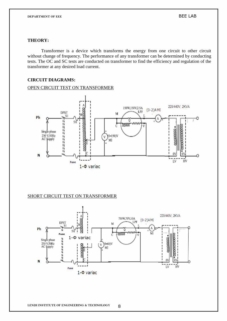
THEORY:
Transformer is a device which transforms the energy from one circuit to other circuit
without change of frequency. The performance of any transformer can be determined by conducting
tests. The OC and SC tests are conducted on transformer to find the efficiency and regulation of the
transformer at any desired load current.
CIRCUIT DIAGRAMS:
OPEN CIRCUIT TEST ON TRANSFORMER
SHORT CIRCUIT TEST ON TRANSFORMER
1-Φ variac Fuse

DEPARTMENT OF EEE BEE LAB
LENDI INSTITUTE OF ENGINEERING & TECHNOLOGY 9
PROCEDURE:
OPEN CIRCUIT TEST
1. Connections are made as per the circuit diagram.
2. By varying single phase variac, the rated input voltage to be applied on low voltage side of the
transformer.
3. Now take down the readings of ammeter, voltmeter and wattmeter.
SHORT CIRCUIT TEST
1. Connections are made as per the circuit diagram.
2. By varying the single phase varic, the rated current is applied to high voltage side of the
transformer.
3. Now take down the readings of voltmeter and wattmeter
TABULAR FORMS:
OPEN CIRCUIT TEST:
S.NO Voc (Volts) Ioc (Amps) Woc(watts)
1
SHORT CIRCUIT TEST:
S.NO Vsc (Volts) Isc (Amps) Wsc(watts)
1
VOLTAGE REGULATION CHARACTERISTICS:
S.No % load Sin Φ Lagging P.F full load
Regulation
Leading P.F full load
Regulation
1 0 1
2 0.2 0.97
3 0.4 0.91
4 0.6 0.8
5 0.8 0.6
6 1 0
EFFICIENCY CHARACTERISTICS:
Load ,X
Let Cos
Φ=0.8
Let Cos Φ=1
Efficiency, η Efficiency, η
x=1/4
x=1/2
x=3/4
x=1

DEPARTMENT OF EEE BEE LAB
LENDI INSTITUTE OF ENGINEERING & TECHNOLOGY 10
MODEL CALUCALATIONS:
=
=
=
Efficiency at Full load,
KVA = ___ ,Woc =_____W , Wsc = ____W
Percentage Regulation for lagging Power Factor:
% R =
=
Percentage Regulation for leading Power Factor:
% R =
=
MODEL GRAPHS:
Efficiency Graph:
Percentage Regulation Graph:
DEPARTMENT OF EEE BEE LAB
LENDI INSTITUTE OF ENGINEERING & TECHNOLOGY 11
PRECAUTIONS:
1. Avoid the loose connections.
2. Avoid connecting of meters directly to the machines.
3. Switch OFF the supply before making the connections.
4. Do not touch the bare conductors.
5. Avoid parallax error while making observations.
RESULT:
OUTCOME:
Viva questions:
1. What is a transformer?
2. Why transformer rated in KVA?
3. What are the losses present in a transformer?
4. What are the applications of transformer?
5. What is voltage regulation of a transformer?

DEPARTMENT OF EEE BEE LAB
LENDI INSTITUTE OF ENGINEERING & TECHNOLOGY 12
Exp No: 3 Date:
BRAKE TEST ON THREE PHASE INDUCTION MOTOR
AIM: To find the performance characteristics of three phase induction motor.
NAME PLATE DETAILS:
S.No Specifications Rating
1 Power 3 HP
2 Voltage 415V
3 Current 6A
4 Speed 1440rpm
5 Frequency 50Hz
6 PF 0.8
APPARATUS:
Sl.
Equipment Type Range Quantity
No.
1 Voltmeter MI (0-600)V 1 no
2 Ammeter MI (0-10)A 1 no
10A/600V UPF 1 no
3 Wattmeter Electro dynamo meter type
10A/600V LPF 1 no
4 Tachometer Digital 0-9999 RPM 1 no
5 Connecting Wires ***** ***** Required
CIRCUIT DIAGRAM:

DEPARTMENT OF EEE BEE LAB
LENDI INSTITUTE OF ENGINEERING & TECHNOLOGY 13
THEORY: It is the direct method to find the efficiency of the induction motor. In this test the braking
of the rotor is done with the help of the belt which surrounds the pulley by using spring balances.
When the braking power is increased by tightening the springs then the line current is increased.
PROCEDURE:
1. Connections are made as per the circuit diagram.
2. With the help of three phase variac, start the machine and run it at no-load. Take the
readings of all meters and measure the speed.
3. Gradually tightening the belt, apply the load in steps.
4. At each load take the readings of all meters and measure the speed.
5. Pour water into pulley and cool it when motor is heated.
6. When the full load is reached, slowly reduce the load and stop the machine by disconnected
the supply.
S.
No
Input
Voltage
(V)
Input
Current
(A)
Speed,
N
(rpm)
W1 W2
Spring
Balance
Torque
N-m Pin=
W1+W2
(W)
Pout,
(W)
η=Pout/
Pin X 100
(%) S1 S2
1
2
3
4
5
6
7
8
CALCULATIONS:
Torque = 9.81(S1-S2) R N-m
Output Power = 2πNT/60
Input Power = W1+W2
% Efficiency = (Output/ Input) x100
PRECAUTIONS:
1. Avoid loose connections.
2. Take the readings without parallax error.
3. Double check the circuit before giving the supply.
4. The motor armature rheostat in maximum position and motor field rheostat in minimum position.

DEPARTMENT OF EEE BEE LAB
LENDI INSTITUTE OF ENGINEERING & TECHNOLOGY 14
RESULT:
OUTCOME:
Viva questions:
1. Explain the working principle of an Induction Motor?
2. What are the types of Induction Motor?
3. Draw the performance characteristics of Induction Motor?
4. Draw the equivalent circuit of Induction Motor?
5. What are the applications of Induction Motor?

DEPARTMENT OF EEE BEE LAB
LENDI INSTITUTE OF ENGINEERING & TECHNOLOGY 15
Exp No: 4 Date:
REGULATION OF A THREE-PHASE ALTERNATOR
AIM: To predict the regulation of Three Phase Alternator using synchronous impedance method.
NAME PLATE DETAILS:
S.No Specifications Rating
DC Motor(Prime
Mover) 3- ɸ Alternator
1 KW 5HP 3.2KW
2 Voltage 220V 415V
3 Current 12A 4.2A
4 Speed 1500 rpm 1500 rpm
5 Exctn Shunt Wound External
6 Voltage 220V 220
7 Field current 0.6A 1.4
APPARATUS:
Sl.
Equipment
Type
Range Quantity
No.
1 Voltmeter MI (0-300/600)V 1 no
2 Ammeter MI (0-10)A 1 no
300 Ω /2A 2 no
3 Rheostat Wire-wound
4 Tachometer Digital 0-10000 rpm 1 no
5 Connecting Wires ***** ***** Required
THEORY:
As the load changes the terminal voltage of an alternator is also changes the magnitude of
this change depends not only on the load but also on load power factor. The voltage regulation of an
alternator is defined as the raise in voltage when the full load is removed (Field excitation and
speed remaining same) divided by the rated terminal voltage.
%Regulation = (Eo – V)/V X100

DEPARTMENT OF EEE BEE LAB
LENDI INSTITUTE OF ENGINEERING & TECHNOLOGY 16
CIRCUIT DIAGRAM:
PROCEDURE:
1. Connections are made as per the circuit diagram.
2. Switch ON the 220v DC supply.
3. Start the DC Motor using 3 point starter.
4. Adjust the speed of the motor to the rated speed using armature regulator and if necessary with
field regulators.
5. Excite the field winding and vary the field current in steps of 0.1 amps and note down the
corresponding readings of voltmeter, keeping the speed constant.
6. Repeat the procedure till 110 to 129 % of the rated voltage is reached.
7. Reduce the field current to ‘0’ and close the ‘TPST’ switch.
8. Vary the field current to ‘0’ and close the ‘TPST’ switch in steps of 0.1 amps and note down the
corresponding ammeter readings, keeping the speed constant.
9. The procedure is Repeated till rated current is reached

DEPARTMENT OF EEE BEE LAB
LENDI INSTITUTE OF ENGINEERING & TECHNOLOGY 17
TABULAR FORM:
OPEN CIRCUIT CHARACTERITICS:
S.NO If (amps) Voc (volts)
1
2
3
4
5
6
SHORT CIRCUIT CHARACTERITICS:
S.NO If (amps) Isc (amps)
1
VOLTAGE REGULATION CHARACTERISTICS:
S.No Cos Φ Sin Φ Lagging P.F full load Eo Leading P.F full load Eo
1 0.2 0.97
2 0.4 0.91
3 0.6 0.8
4 0.8 0.6
5 1 0
MODEL CALUCALATIONS:
= ________V
Z
=______Ω
= 1.5 X 4.2 = 6.3Ω
= ________Ω
For lagging P.F: By substituting all the values in Eo, We will get

DEPARTMENT OF EEE BEE LAB
LENDI INSTITUTE OF ENGINEERING & TECHNOLOGY 18
For leading P.F:
By substituting all the values in Eo, We will get
Percentage Regulation: % R =
MODEL GRAPH:
PRECAUTIONS:
1. Avoid loose connections.
2. Switch OFF the Supply before making connections.
3. Do not touch the bare conductors.
4. Avoid parallax error while making observations.
RESULT:
OUTCOME:
Viva questions:
1. What is an Alternator?
2. What is the principle of alternator?
3. Define regulation of an Alternator?
4. What are the different methods for finding regulation of an alternator?
5. What are the applications of an alternator?

DEPARTMENT OF EEE BEE LAB
LENDI INSTITUTE OF ENGINEERING & TECHNOLOGY 19
Exp No: 5 Date:
SPEED CONTROL OF DC SHUNT MACHINE
AIM: To determine the speed characteristics of D.C. shunt motor by
1. Field Control Method
2. Armature Control Method
NAME PLATE DETAILS:
S.No Specifications Rating
1 Rated Voltage 220V
2 Rated Speed 1500rmp
3 Field Current 1.2A
APPARATUS:
THEORY:
The term speed control means intentional sped variation, carried out manually or
automatically. DC motors are most suitable for wide range speed control and are therefore
indispensible for many adjustable speed drives. The speed of a motor is given by Wm = (Vt-
IaRa)/Kaф Where Ka – armature constant = PZ/2∏A and ф is the flux per pole. Hence it follows
that, for a DC motor, there are basically two methods of speed control and these are:
1. Variation of the field flux.
2. Variation of armature terminal voltage.
Variation of the field flux: This method of speed control, also called as flux weakening method or
filed current control method gives speeds above the base speed only. Base speed is nothing but the
rated speed of the machine. This is one of the simplest and economical methods and is, therefore
extensively used in modern electric drives. Under steady state running conditions, if the field circuit
resistance is increased, the field current and hence the field flux are reduced. Since the rotor speed
cannot change suddenly due to inertia, a decrease in field current causes a reduction of counter emf.
As a result of it, more current flows through armature. The percentage increase in armature current
is much more than the percentage decrease in the field current. In view of this, the electromagnetic
torque is increased and this being more than the load torque, the motor gets accelerated.
The disadvantages of this method are:
a) The armature may get over heated at higher speeds, because the increased armature
current results in more ohmic losses whereas cooling by ventilation does not improve
proportionally.
b) If the field flux is weakened considerably, the speed becomes very high and due to these
changes; the motor operation may become unstable.

DEPARTMENT OF EEE BEE LAB
LENDI INSTITUTE OF ENGINEERING & TECHNOLOGY 20
Variation of armature terminal voltage: If the voltage applied to the armature changes the speed
changes directly with it. Using this method, speeds below rated speeds are attained.
CIRCUIT DIAGRAM:
For Field Control Method:
For Armature Control Method:
PROCEDURE:
For Field Control method:
1. The connections are made as per the circuit diagram.
2. The field rheostat is kept at minimum position.
3. The motor is started with the help of three point starter.
4. Rf is increased in steps thereby decreasing the field current. The values of If and speed are noted
down.
For Armature Control Method:
1. The connections are made as per the circuit diagram.
2. The armature rheostat is kept at maximum position.
3. The motor is started with the help of the starter.
Fuse

DEPARTMENT OF EEE BEE LAB
LENDI INSTITUTE OF ENGINEERING & TECHNOLOGY 21
4. The armature rheostat is varied from maximum value to minimum value in steps.
5. The speed for each value of Va is noted down.
TABULAR FORM:
For Field Control Method:
S.No. Field Current, ISh(A) Speed,N(rpm)
1
2
3
4
5
For Armature Control Method:
S.No. Arm. Voltage,Va (v) Speed,N(rpm)
1
2
3
4
5
MODEL GRAPH:
Armature voltage control: Field control method:
PRECAUTIONS:
1. Avoid loose connections.
2. Switch OFF the Supply before making connections.
3. Rheostat positions are checked before switching on the motor
4. Do not touch the bare conductors.

DEPARTMENT OF EEE BEE LAB
LENDI INSTITUTE OF ENGINEERING & TECHNOLOGY 22
5. Avoid parallax error while making observations.
RESULT:
OUTCOME:
Viva questions:
1. Why to control the speed of a DC Motor?
2. What is ment by armature reaction?
3. Draw the characteristics of DC shunt motor?
4. What is the expression for back EMF?
5. What are the applications of Dc Motors?

DEPARTMENT OF EEE BEE LAB
LENDI INSTITUTE OF ENGINEERING & TECHNOLOGY 23
Exp No: 6 Date:
BRAKE TEST ON A DC SHUNT MOTOR
AIM: To obtain the performance characteristic curves of a D.C. shunt motor by conducting brake
test on it
NAME PLATE DETAILS:
APPARATUS:
THEORY:
It is a simple method testing DC machines and consists of applying a brake to a water
cooled drum mounted on the motor shaft. A rope is wound round the pulley and its two ends are
attached to two spring balances S1 & S2. The tension of the rope can be adjusted with the help of
swivels. The force acting tangentially on the drum is equal to the difference between the readings of
the
a) This test can be used for small motors only, as, in the case of large motors, it is difficult to
dissipate the large amount of heat generated at the brake.
b) Where the output power exceeds about 2 H.P., or where the test is of long duration, it’s
necessary to use water –cooled pulley.

DEPARTMENT OF EEE BEE LAB
LENDI INSTITUTE OF ENGINEERING & TECHNOLOGY 24
CIRCUIT DIAGRAM:
PROCEDURE:
1. The connections are made as per the circuit diagram.
2. Initially the starter is in off position.
3. The field rheostat is in minimum position.
3. 220V DC supply is applied by closing the DPST Switch.
4. The DC motor is started slowly with the starter and brought to the rated speed.
5. Load is applied on the drum gradually in steps by tightening the belt around it.
6. The readings of the ammeter & voltmeter, two spring balances and the speed at every step are
noted.
7. Drum is cooled throughout the loading period by pouring water.
8. The experiment is continued till the full load on the motor is impressed.
9. The machine is switched OFF by opening the DPST switch.
TABULAR FORM:
S.No
Supply
Voltage(
V)
Arm
Current Ia
(A)
Speed,
N
(rpm)
Spring
Balance Field
Current
, Ish(A)
Torqu
e,
T(N-
m)
Pin,
(W)
Pout,
(W)
η=Pou
t/Pin X
100
(%) S1 S2
1
2
3
4
5
6
7

DEPARTMENT OF EEE BEE LAB
LENDI INSTITUTE OF ENGINEERING & TECHNOLOGY 25
MODEL CALUCALATIONS:
Let
S1 = Readings on spring balance 1 in Kgf.wt.
S2 = Readings on spring balance 2 in Kgf.wt.
The net force applied on the brake drum is (S1 – S2) Kgf.Wt.
If R = radius of the pulley in meters (15.2 Cm)
N = Motor speed in rpm then,
Shaft torque, T, developed by the motor is:
T = 9.81 × (S1 – S2) × R N-m
Output power = 2πNT/60 Watts
Input power = V (Ia + Ish) Watts
%Efficiency = Output power / Input power X 100
MODEL GRAPH:
PRECAUTIONS:
1. Avoid loose connections.
2. Switch OFF the Supply before making connections.
3. Rheostat positions are checked before switching on the motor
4. Do not touch the bare conductors.
5. Avoid parallax error while making observations.
RESULT:

DEPARTMENT OF EEE BEE LAB
LENDI INSTITUTE OF ENGINEERING & TECHNOLOGY 26
OUTCOME:
Viva questions:
1. What is the principle of DC Motor?
2. What is the need of starter?
3. What are the types of speed control methods for DC motor?
4. What are the parts of a DC motor?
5. What are losses present in Dc motor?

DEPARTMENT OF EEE BEE LAB
LENDI INSTITUTE OF ENGINEERING & TECHNOLOGY 27
Exp No: 7 Date:
P-N JUNCTION DIODE CHARACTERISTICS
AIM: a) To observe and draw the V-I Characteristics of a P-N Junction diode in Forward and
Reverse bias. b) To calculate the cut-in voltage at which diode conducts.
c) To calculate static and dynamic resistance.
APPARATUS REQUIRED:
S.No Name of the apparatus Qty Range
1 PN Diode IN4007 1 -
2 Regulated power supply 1 0-30V
3 Voltmeter 2 0-20V,0-1V
4 Ammeter 2 0-20mA,0-750 µA
5 Resistor 1 1KΩ
6 Bread board 1 -
7 Connecting wires - -
THEORY: A p-n junction diode conducts only in one direction, the V-I characteristics of p-n diode is a
curve plotted between the voltage across diode and current through the diode. When external voltage is zero, circuit is open and the potential barrier does not allow the current to flow. Therefore, the circuit current is zero. When P-type Anode is connected to +ve terminal and N- type Cathode is connected to the –ve terminal of supply voltage the diode is considered to be operating under forward bias condition. When the voltage across the diode is increased in the forward biased condition, the potential barrier is reduced and is altogether eliminated at some forward voltage, resulting in the current to flow through the diode and the circuit. The diode is now said to be in the ON state and the current keeps on increasing with an increase in the forward voltage.
A p-n junction diode is considered to be operating under reverse bias condition when the N-type cathode is connected to +ve terminal and P-type Anode is connected to the –ve terminal of supply voltage. Under reverse bias condition potential barrier across the junction increases with a corresponding rise in the supply voltage, hence junction resistance becomes very high and a very small reverse saturation current flows in the circuit due to minority charge carriers. The diode is now said to be in the OFF state.
CIRCUIT DIAGRAM:
Forward Bias:

DEPARTMENT OF EEE BEE LAB
LENDI INSTITUTE OF ENGINEERING & TECHNOLOGY 28
Reverse Bias:
Model Waveform:
PROCEDURE:
Forward Bias:- 1. Connections are made as per the circuit diagram. 2. Under forward bias, the RPS +ve terminal is connected to the anode of diode and RPS –ve
Terminal is connected to the cathode of the diode. 3. Switch on the power supply and increase the input voltage (supply voltage) in Steps. 4. Note down the corresponding current flowing through the diode and voltage across the Diode for
each and every step of the input voltage. 5. Tabulate the readings of voltage and current. 6. Plot the graph between voltage and current. 7. Find the cut-in voltage in forward bias. 8. Calculate the static and dynamic resistances. Reverse Bias: 1. Connections are made as per the circuit diagram. 2. Under reverse bias, the RPS -ve terminal is connected to the anode of diode and RPS +ve
Terminal is connected to the cathode of the diode. 3. Switch on the power supply and increase the input voltage (supply voltage) in Steps. 4. Note down the corresponding current flowing through the diode and voltage across the Diode for
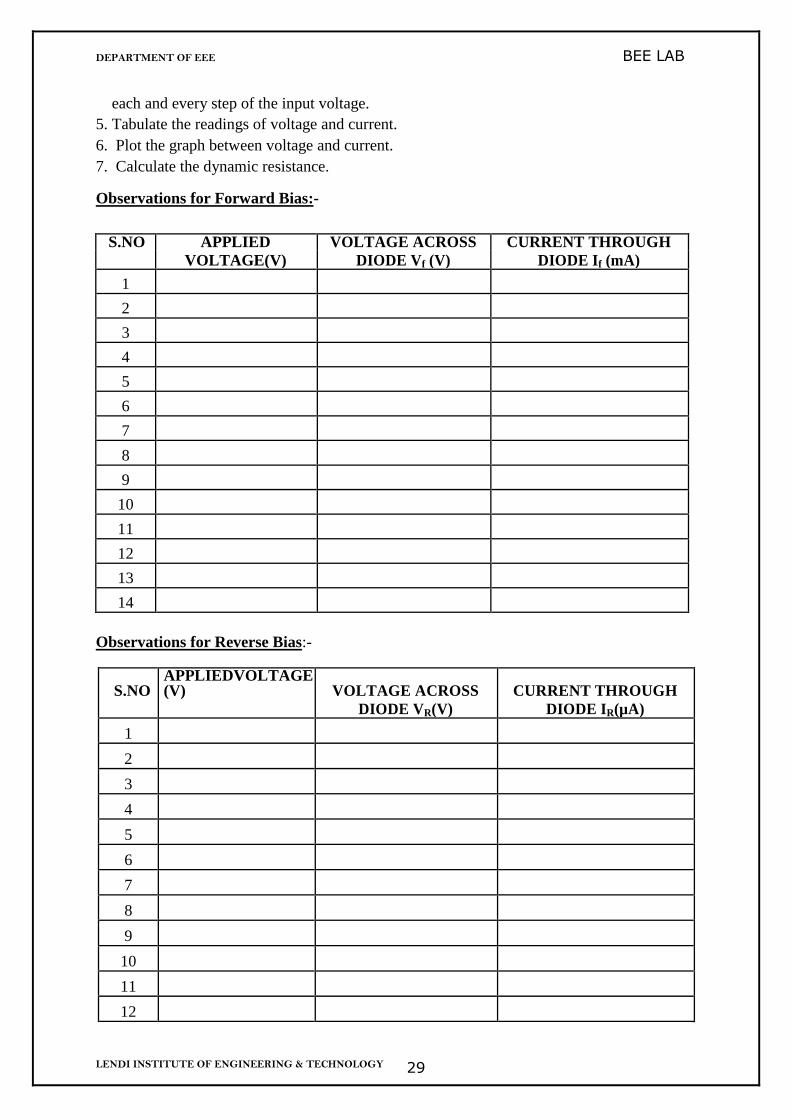
DEPARTMENT OF EEE BEE LAB
LENDI INSTITUTE OF ENGINEERING & TECHNOLOGY 29
each and every step of the input voltage. 5. Tabulate the readings of voltage and current. 6. Plot the graph between voltage and current. 7. Calculate the dynamic resistance. Observations for Forward Bias:-
S.NO APPLIED VOLTAGE ACROSS CURRENT THROUGH VOLTAGE(V) DIODE Vf (V) DIODE If (mA)
1
2
3
4
5
6
7
8
9
10
11
12
13
14
Observations for Reverse Bias:-
S.NO APPLIEDVOLTAGE(V) VOLTAGE ACROSS CURRENT THROUGH
DIODE VR(V) DIODE IR(µA)
1
2
3
4
5
6
7
8
9
10
11
12
DEPARTMENT OF EEE BEE LAB
LENDI INSTITUTE OF ENGINEERING & TECHNOLOGY 30
Calculations: Forward Bias:
Static resistance RD = VD/ID=_____KΩ
Dynamic resistance rd = ∆Vd/ ∆Id =_______KΩ Reverse Bias:
Static resistance RD = VD/ID =____KΩ
Dynamic resistance rd = ∆Vd/ ∆Id=_____KΩ
Applications: As Rectifier in DC Power Supplies.
In Demodulation or Detector Circuits.
As DC Restorer in clamping networks.
In clipping circuits used for waveform generation.
As switches in digital logic circuits.
PRECAUTIONS:
1. Avoid loose connections.
2. The supply voltage should not exceed the rating of the component.
3. Meters should be connected properly according there polarity.
RESULTS:
Forward and Reverse Bias characteristics of p-n diode are obtained. Cut-in voltage = Static Resistance in Forward Bias = Dynamic resistance in Forward Bias = Static Resistance in Reverse Bias = Dynamic resistance in Reverse Bias =
OUTCOME:
Viva Questions: 1. Define depletion region of a diode?
2. What is meant by transition & space charge capacitance of a diode?
3. Is the V-I relationship of a diode Linear or Exponential?
4. Define cut-in voltage of a diode and specify the values for Si and Ge diodes?
5. What are the applications of a p-n diode?
6. Draw the ideal characteristics of P-N junction diode? 7. What is the diode equation? 8. What is PIV? 9. What is the break down voltage? 10. What is the effect of temperature on PN junction diodes? 11. How does the diode act as a switch? 12. Differentiate cut-in and cut-off voltages?

DEPARTMENT OF EEE BEE LAB
LENDI INSTITUTE OF ENGINEERING & TECHNOLOGY 31
Exp No: 8 Date:
TRANSISTOR COMMON EMITTER CHARACTERSTICS
AIM: To draw the input and output characteristics of transistor connected in CE Configuration
APPARATUS REQUIRED:
S.No Name of the apparatus Qty Range
1 Transistor(BC 107) 1 -
2 Regulated power supply 2 0-30V
3 Voltmeter 2 0-20V
4 Ammeter 2 0-20mA,0-750 µA
5 Resistor 1 1KΩ
6 Bread board 1 -
THEORY: A transistor is a three terminal device. The terminals are emitter, base, collector. In common
emitter configuration, input voltage is applied between base and emitter terminals and output is
taken across the collector and emitter terminals. Therefore the emitter terminal is common to both
input and output.
The input characteristics resemble that of a forward biased diode curve. This is expected
since the Base-Emitter junction of the transistor is forward biased. As compared to CB arrangement
IB increases less rapidly with VBE. Therefore input resistance of CE circuit is higher than that of CB
circuit.
The output characteristics are drawn between Ic and VCE at constant IB. The collector current
varies with VCE until few volts only. After this the collector current becomes almost constant, and
independent of VCE. The value of VCE up to which the collector current changes with VCE is known
as Knee voltage. The transistor always operated in the region above Knee voltage, IC is always
constant and is approximately equal to IB. It operates in three regions: active region, cut-off region
and saturation region.
Active region: When E-B junction is forward biased and C-B junction is reverse biased then the transistor is said to be in active region. Cut-off region: When E-B junction is reverse biased and C-B junction is reverse biased then the transistor is said to be in cut-off region. Saturation region: When E-B junction is forward biased and C-B junction is forward biased then the transistor is said to be in saturation region.
The current amplification factor of CE configuration is given by β = ΔIC/ΔIB

DEPARTMENT OF EEE BEE LAB
LENDI INSTITUTE OF ENGINEERING & TECHNOLOGY 32
CIRCUIT DIAGRAM:
Input Characteristics: PROCEDURE:
Input Characteristics: 1. Connect the circuit as per the circuit diagram. 2. For plotting the input characteristics the output voltage VCE is kept constant at 1V
and for different values of VBE. Note down the values of IC. 3. Repeat the above step by keeping VCE at 2V and 4V. 4. Tabulate all the readings. 5. Plot the graph between VBE and IB for constant VCE.
Observations:
Input Characteristics:
S.No
VCE = 1V VCE = 2V
VBE(V) IB(μA) VBE(V) IB(μA)
1
2
3
4
5
6
7
8
9
10

DEPARTMENT OF EEE BEE LAB
LENDI INSTITUTE OF ENGINEERING & TECHNOLOGY 33
Output Characteristics:
Output characteristics:
1. Connect the circuit as per the circuit diagram.
2. For plotting the output characteristics the input current IB is kept constant at 10μA and for
different values of VCE, note down the values of IC. 3. Repeat the above step by keeping IB at 75 μA and 100 μA. 4. Tabulate the all the readings. 5. Plot the graph between VCE and IC for constant IB.
Output Characteristics:
S.No IB = 50 μA IB = 70μA
VCE(V) IC(mA) VCE(V) IC(mA)
1
2
3
4
5
6
7
8
9
10
Model Graphs:
Input Characteristics:- Output Characteristics:-
DEPARTMENT OF EEE BEE LAB
LENDI INSTITUTE OF ENGINEERING & TECHNOLOGY 34
Applications:
1. Acts as a switch
2. As an amplifier
3. As an inverter
4. In oscillators
PRECAUTIONS:
1. Avoid loose connections.
2. The supply voltage should not exceed the rating of the component.
3. Meters should be connected properly according there polarity.
RESULT:
Outcome:
Viva Questions:
1. What are the input and output impedances of CE configuration?
2. Identify various regions in the output characteristics?
3. Define current gain in CE configuration?
4. Why CE configuration is preferred for amplification?
5. What is the phase relation between input and output?
6. Draw diagram of CE configuration for PNP transistor?
7. What is the power gain of CE configuration?
8. What are the applications of CE configuration?

DEPARTMENT OF EEE BEE LAB
LENDI INSTITUTE OF ENGINEERING & TECHNOLOGY 35
Exp No: 9 Date:
FULL-WAVE RECTIFIER AIM: - Design the Full-Wave Rectifier
a) To obtain the load regulation characteristics of full-wave rectifier b) To determine the ripple factor and efficiency of a full-wave rectifier.
1. with Filter
2. without Filter
APPARATUS REQUIRED:
S.No Name of the apparatus Qty Range
1 Transformer 1 (9-0-9)
2 PN diode,(IN4007) 2 -
3 Multimeter 1 -
4 Filter Capacitor 1 100μF/25v
5 Load Resistor 1 Decade Resistance
Box
6 Bread board 1 -
7 CRO 1 -
THEORY: The circuit of a center-tapped full wave rectifier uses two diodes D1&D2. During positive
half cycle of secondary voltage (input voltage), the diode D1 is forward biased and D2 is reverse biased. The diode D1 conducts and current flows through load resistor RL. During negative half cycle, diode D2 becomes forward biased and D1 reverse biased. Now, D2 conducts and current flows through the load resistor RL in the same direction. There is a continuous current flow through the load resistor RL, during both the half cycles making the direction of current unidirectional as show in the model graph.
The difference between full wave and half wave rectification is that a full wave rectifier
allows unidirectional (one way) current to the load during the entire 360 degrees of the input signal
and half-wave rectifier allows the current only during one half cycle (180 degree).
CIRCUIT DIAGRAM:
With Out Filter:
DEPARTMENT OF EEE BEE LAB
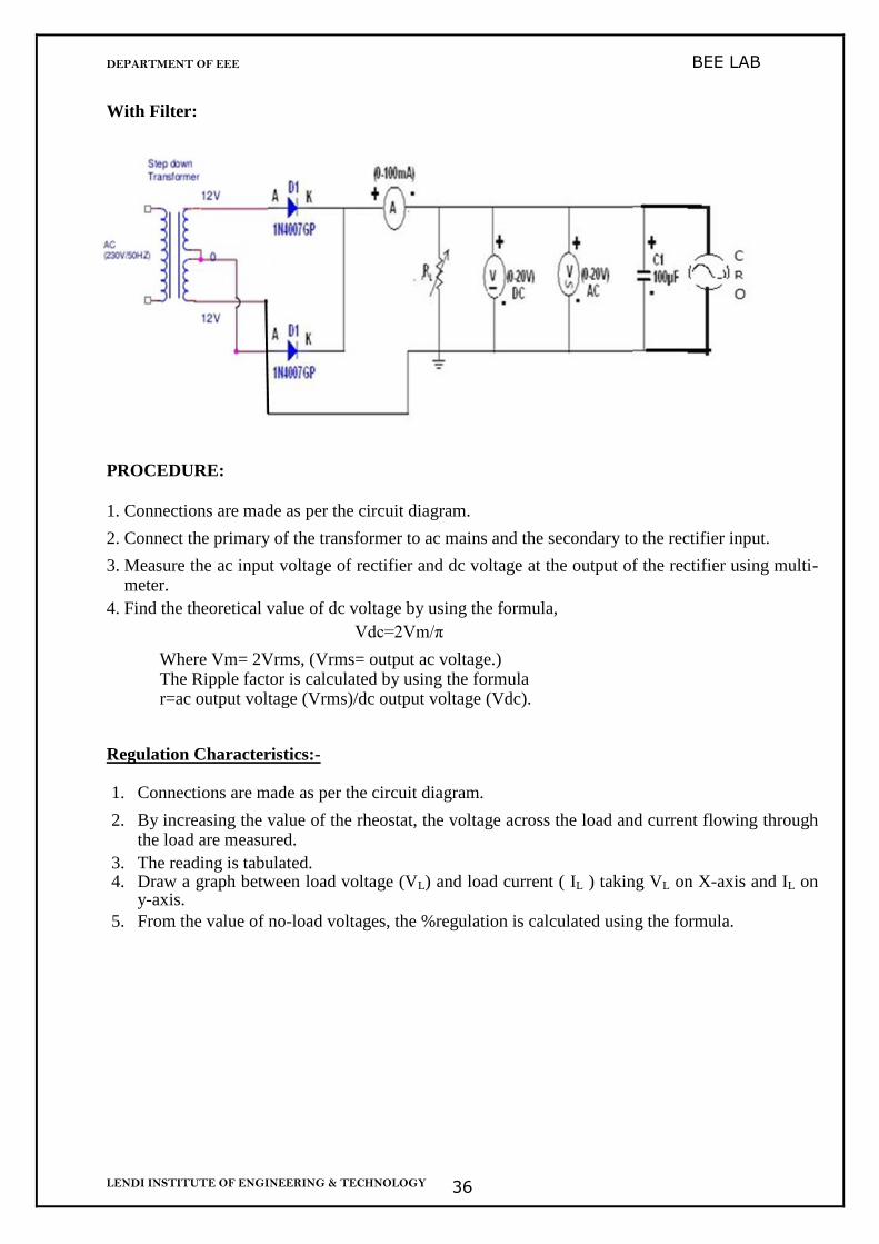
LENDI INSTITUTE OF ENGINEERING & TECHNOLOGY 36
With Filter: PROCEDURE:
1. Connections are made as per the circuit diagram. 2. Connect the primary of the transformer to ac mains and the secondary to the rectifier input. 3. Measure the ac input voltage of rectifier and dc voltage at the output of the rectifier using multi-
meter. 4. Find the theoretical value of dc voltage by using the formula,
Vdc=2Vm/π
Where Vm= 2Vrms, (Vrms= output ac voltage.) The Ripple factor is calculated by using the formula r=ac output voltage (Vrms)/dc output voltage (Vdc).
Regulation Characteristics:- 1. Connections are made as per the circuit diagram.
2. By increasing the value of the rheostat, the voltage across the load and current flowing through
the load are measured. 3. The reading is tabulated. 4. Draw a graph between load voltage (VL) and load current ( IL ) taking VL on X-axis and IL on
y-axis. 5. From the value of no-load voltages, the %regulation is calculated using the formula.
DEPARTMENT OF EEE BEE LAB
LENDI INSTITUTE OF ENGINEERING & TECHNOLOGY 37
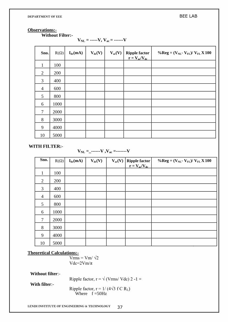
Observations:-
Without Filter:- VNL = -----V, Vac = ------V
Sno. R(Ω) Idc(mA) Vdc(V) Vac(V) Ripple factor %Reg = (VNL- VFL)/ VFL X 100
r = Vac/Vdc
1 100
2 200
3 400
4 600
5 800
6 1000
7 2000
8 3000
9 4000
10 5000
WITH FILTER:- VNL =_------V ,Vac =-------V
Sno. R(Ω) Idc(mA) Vdc(V) Vac(V) Ripple factor %Reg = (VNL- VFL)/ VFL X 100
r = Vac/Vdc
1 100
2 200
3 400
4 600
5 800
6 1000
7 2000
8 3000
9 4000
10 5000 Theoretical Calculations:-
Vrms = Vm/ √2 Vdc=2Vm/π
Without filter:-
Ripple factor, r = √ (Vrms/ Vdc) 2 -1 =
With filter:- Ripple factor, r = 1/ (4√3 f C RL)
Where f =50Hz

DEPARTMENT OF EEE BEE LAB
LENDI INSTITUTE OF ENGINEERING & TECHNOLOGY 38
C =100µF RL=1KΩ
Practical Calculations:-
Without filter:- Vac= Vdc= Ripple factor, r=Vac/Vdc =
With filters:- Vac= Vdc= Ripple factor, r=Vac/Vdc =
PRECAUTIONS:
1. Avoid loose connections.
2. The supply voltage should not exceed the rating of the component.
3. Meters should be connected properly according there polarity.
RESULT:
OUTCOME:
Viva Questions:-
1. Define regulation of the full wave rectifier? 2. Define peak inverse voltage (PIV)? And write its value for Full-wave rectifier? 3. If one of the diode is changed in its polarities what wave form would you get? 4. Does the process of rectification alter the frequency of the waveform? 5. What is ripple factor of the Full-wave rectifier? 6. What is the necessity of the transformer in the rectifier circuit?
DEPARTMENT OF EEE BEE LAB
LENDI INSTITUTE OF ENGINEERING & TECHNOLOGY 39
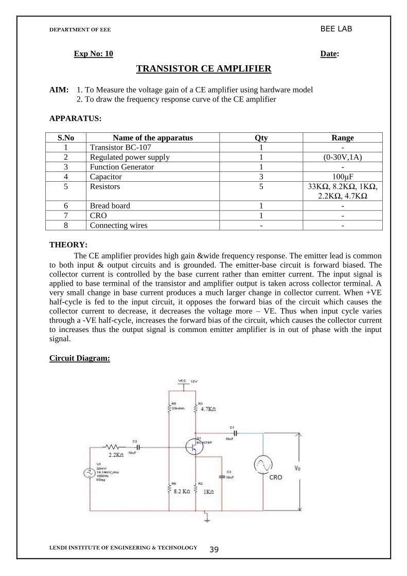
Exp No: 10 Date:
TRANSISTOR CE AMPLIFIER
AIM: 1. To Measure the voltage gain of a CE amplifier using hardware model
2. To draw the frequency response curve of the CE amplifier
APPARATUS:
S.No Name of the apparatus Qty Range
1 Transistor BC-107 1 -
2 Regulated power supply 1 (0-30V,1A)
3 Function Generator 1 -
4 Capacitor 3 100μF
5 Resistors 5 33KΩ, 8.2KΩ, 1KΩ,
2.2KΩ, 4.7KΩ
6 Bread board 1 -
7 CRO 1 -
8 Connecting wires - -
THEORY: The CE amplifier provides high gain &wide frequency response. The emitter lead is common
to both input & output circuits and is grounded. The emitter-base circuit is forward biased. The collector current is controlled by the base current rather than emitter current. The input signal is applied to base terminal of the transistor and amplifier output is taken across collector terminal. A very small change in base current produces a much larger change in collector current. When +VE half-cycle is fed to the input circuit, it opposes the forward bias of the circuit which causes the collector current to decrease, it decreases the voltage more – VE. Thus when input cycle varies through a -VE half-cycle, increases the forward bias of the circuit, which causes the collector current to increases thus the output signal is common emitter amplifier is in out of phase with the input signal.
Circuit Diagram:

DEPARTMENT OF EEE BEE LAB
LENDI INSTITUTE OF ENGINEERING & TECHNOLOGY 40
PROCEDURE: 1. Connect the circuit as shown in circuit diagram. 2. Apply the input of 20mV peak-to-peak and 1 KHz frequency using Function Generator.
3. Measure the Output Voltage Vo (p-p) for various load resistors.
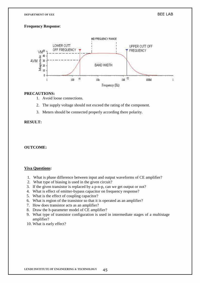
4. Tabulate the readings in the tabular form. 5. The voltage gain can be calculated by using the expression Av= (V0/Vi) . 6. For plotting the frequency response the input voltage is kept Constant at 20mV peak-to-peak and the frequency is varied from 100Hz to 1MHz Using function generator. 7. Note down the value of output voltage for each frequency. 8. All the readings are tabulated and voltage gain in dB is calculated by Using The expression Av=20 log10 (V0/Vi) 9. A graph is drawn by taking frequency on x-axis and gain in dB on y-axis On Semi-log graph.
The band width of the amplifier is calculated from the graph Using the expression, Bandwidth, BW=f2-f1
Where f1 lower cut-off frequency of CE amplifier, and f2 upper cut-off frequency of CE amplifier
The bandwidth product of the amplifier is calculated using the Expression Gain Bandwidth product =3-dBmidband gain X Bandwidth
Observations: Input voltage Vi=20mV
Frequency Response: Vi=20mv
FREQUENCY(Hz) OUTPUT GAIN IN dB VOLTAGE (V0) Av=20 log10 (V0/Vi)
300
600
900
1K
2K
3K
4K
5K
6K
7K
8K
9K
10K
20K
30K
40K
50K
60K
70K
80K
90K
100K
200K
300K
400K
500K
600K

DEPARTMENT OF EEE BEE LAB
LENDI INSTITUTE OF ENGINEERING & TECHNOLOGY 41
Model Graphs:
Input Wave Form:
Output Wave Form Frequency Response:
PRECAUTIONS:
1. Avoid loose connections.
2. The supply voltage should not exceed the rating of the component.
3. Meters should be connected properly according there polarity.

DEPARTMENT OF EEE BEE LAB
LENDI INSTITUTE OF ENGINEERING & TECHNOLOGY 42
RESULT:
OUTCOME:
Viva Questions:
1. What is phase difference between input and output waveforms of CE amplifier? 2. What type of biasing is used in the given circuit? 3. If the given transistor is replaced by a p-n-p, can we get output or not? 4. What is effect of emitter-bypass capacitor on frequency response? 5. What is the effect of coupling capacitor? 6. What is region of the transistor so that it is operated as an amplifier? 7. How does transistor acts as an amplifier? 8. Draw the h-parameter model of CE amplifier?
9. What type of transistor configuration is used in intermediate stages of a multistage
amplifier? 10. What is early effect?
DEPARTMENT OF EEE BEE LAB
LENDI INSTITUTE OF ENGINEERING & TECHNOLOGY 43
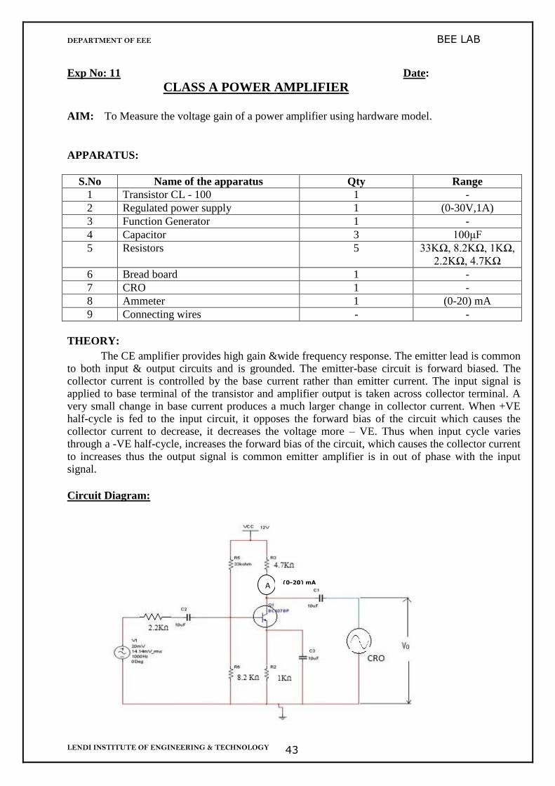
Exp No: 11 Date:
CLASS A POWER AMPLIFIER
AIM: To Measure the voltage gain of a power amplifier using hardware model.
APPARATUS:
S.No Name of the apparatus Qty Range
1 Transistor CL - 100 1 -
2 Regulated power supply 1 (0-30V,1A)
3 Function Generator 1 -
4 Capacitor 3 100μF
5 Resistors 5 33KΩ, 8.2KΩ, 1KΩ,
2.2KΩ, 4.7KΩ
6 Bread board 1 -
7 CRO 1 -
8 Ammeter 1 (0-20) mA
9 Connecting wires - -
THEORY: The CE amplifier provides high gain &wide frequency response. The emitter lead is common
to both input & output circuits and is grounded. The emitter-base circuit is forward biased. The collector current is controlled by the base current rather than emitter current. The input signal is applied to base terminal of the transistor and amplifier output is taken across collector terminal. A very small change in base current produces a much larger change in collector current. When +VE half-cycle is fed to the input circuit, it opposes the forward bias of the circuit which causes the collector current to decrease, it decreases the voltage more – VE. Thus when input cycle varies through a -VE half-cycle, increases the forward bias of the circuit, which causes the collector current to increases thus the output signal is common emitter amplifier is in out of phase with the input signal.
Circuit Diagram:
A (0-20) mA

DEPARTMENT OF EEE BEE LAB
LENDI INSTITUTE OF ENGINEERING & TECHNOLOGY 44
PROCEDURE: 1. Connect the circuit as shown in circuit diagram. 2. Apply the input of 20mV peak-to-peak and 1 KHz frequency using Function Generator
3. By keeping the input voltage signal constant, measure the output voltage Vo peak to peak and
current.
Observations: Input voltage Vi=20mV
Rc = 4.7KΩ , Vdc=12V
Load frequency = 1K Hz
Ic=1.6A , Vmax = 5/2 = 2.5V
Vo= 5V
Pac= V2
max / 2Rc =__________
W
Pdc= Vdc X Ic = -------W
% η = (Pac/Pdc) X 100 =
Model Graphs:
Input Wave Form:
Output Wave Form:
DEPARTMENT OF EEE BEE LAB
LENDI INSTITUTE OF ENGINEERING & TECHNOLOGY 45
Frequency Response:
PRECAUTIONS:
1. Avoid loose connections.
2. The supply voltage should not exceed the rating of the component.
3. Meters should be connected properly according there polarity.
RESULT:
OUTCOME:
Viva Questions:
1. What is phase difference between input and output waveforms of CE amplifier?
2. What type of biasing is used in the given circuit?
3. If the given transistor is replaced by a p-n-p, can we get output or not?
4. What is effect of emitter-bypass capacitor on frequency response?
5. What is the effect of coupling capacitor?
6. What is region of the transistor so that it is operated as an amplifier?
7. How does transistor acts as an amplifier?
8. Draw the h-parameter model of CE amplifier?
9. What type of transistor configuration is used in intermediate stages of a multistage
amplifier?
10. What is early effect?
DEPARTMENT OF EEE BEE LAB
LENDI INSTITUTE OF ENGINEERING & TECHNOLOGY 46
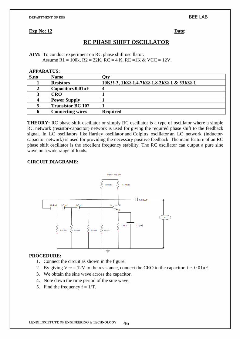
Exp No: 12 Date:
RC PHASE SHIFT OSCILLATOR
AIM: To conduct experiment on RC phase shift oscillator.
Assume R1 = 100k, R2 = 22K, RC = 4 K, RE =1K & VCC = 12V.
APPARATUS:
S.no Name Qty
1 Resistors 10KΩ-3, 1KΩ-1,4.7KΩ-1,8.2KΩ-1 & 33KΩ-1
2 Capacitors 0.01μF 4
3 CRO 1
4 Power Supply 1
5 Transistor BC 107 1
6 Connecting wires Required
THEORY: RC phase shift oscillator or simply RC oscillator is a type of oscillator where a simple
RC network (resistor-capacitor) network is used for giving the required phase shift to the feedback
signal. In LC oscillators like Hartley oscillator and Colpitts oscillator an LC network (inductor-
capacitor network) is used for providing the necessary positive feedback. The main feature of an RC
phase shift oscillator is the excellent frequency stability. The RC oscillator can output a pure sine
wave on a wide range of loads.
CIRCUIT DIAGRAME:
PROCEDURE:
1. Connect the circuit as shown in the figure.
2. By giving Vcc = 12V to the resistance, connect the CRO to the capacitor. i.e. 0.01μF.
3. We obtain the sine wave across the capacitor.
4. Note down the time period of the sine wave.
5. Find the frequency f = 1/T.

DEPARTMENT OF EEE BEE LAB
LENDI INSTITUTE OF ENGINEERING & TECHNOLOGY 47
CALCULATIONS:
Theoretical value
=___________Hz
Where R= 10KΩ , C= 0.01μF
Practical value
f = 1/T = __________Hz
PRECAUTIONS:
1. Avoid loose connections.
2. The supply voltage should not exceed the rating of the component.
3. Meters should be connected properly according there polarity.
RESULT:
OUTCOME:
Viva Questions:
1. What is an Oscillator circuit?
2. What is the main difference between an amplifier and an oscillator?
3. State Barkhausen criterion for oscillation.
4. State the factors on which oscillators can be classified.
5. Give the expression for the frequency of oscillation and the minimum gain required for
sustained oscillations of the RC phase shift oscillator.
6.Why three RC networks are needed for a phase shift oscillator? Can it be two or four?