Embed Size (px)
Citation preview

Basic electrical circuits on the protoboard Darko Androić, Željko Brenčić, Nedeljko Mandić
School exercises in electrical circuits are generally performed using elements on a specific stand with the corresponding connectors for connecting using wires. This allows for simpler and safer connecting of the elements. To perform independent lab exercises, you require a lot of elements (resistors, light bulbs, capacitors, inductor coils, diodes, transistors etc.). They are very expensive and, because of that, schools generally have only one set for frontal exercises. You can also perform exercises on computers, but that way students cannot get the real perception of the real elements nor learn to connect electrical circuits and measure using instruments. Instead of one of these ways, you can perform electrical circuit exercises using a protoboard. A protoboard is a board used to connect different circuits. It is generally used in electronics to check circuits before making printed circuit boards (PCB). The protoboard consists of a series of holes in which you place real circuit elements without using banana connectors. The red line marks the positive pole, and the blue one the negative pole of the power source. Every hole in the same row are on the same electrical potential. The pros of the protoboard are simple usage and a low price, allowing a larger number of students to simultaneously perform independent excercises. The visual design of the circuits on the protoboard is closer to real PCB circuits. This is specifically designed for students of vocational schools and high school students planning on studying electrical science. A minor difficulty is that during the first few uses the protoboard requires the student to be skilled in placing the elements and wires in the holes. Using the protoboard, the students quickly acquire that skill. On the workshop the participants had ten sets to perform their excercises at their disposal. Each set came with a protoboard with a regulated voltage source (3 V, 5 V, 6 V, 9 V, 12 V and 15 V), a universal measuring instrument as well as passive (resistors) and active (diodes and transistors) elements. Using the protoboard and elements, the students performed the following excercises: Ohm's law, Series, parallel and combined resistor connections, recording the I-V graph of a semiconductor diode and transistor amplification.
Protoboard Protoboard connections
116
3. Basic electronic circuits
INTRODUCTION The same exercises are performed on an electronic module and by using Electronics Workbench 1) (The electronics lab in a computer). The aim of this exercise, besides being educational, is: To examine the functionality and ease of use electronic module. To compare the results between the simulation and reality. Electronics Workbench is an electronic lab in a computer. You can easily build an analog or digital circuit schematic, attach simulated test instrument, and turn on the power to see how it works.
RECTIFIER CIRCUITS Half-Wave Rectifier Circuit
General In circuits in which semiconductor diodes are inserted, a current can only flow (on-state range) when the applied current has a certain polarity. If the polarity of the voltage is reversed, the off-state range of the diode becomes effective, preventing current from flowing. In circuits such as these are fed with AC voltage, current only flows during the half-wave at which diode is in the on-state. The other half wave is suppressed. The current in the circuit only flows in one direction. Experiments Examine the rectifying effect of a semiconductor diode in a half-wave rectifier and examine its properties (with and without smoothing capacitor) with the multimeter and the oscilloscope. Procedure Set up the circuit according to Fig.1.1. with the support of Electronics Workbench and measure the DC output voltage Ud with the multimeter and calculate ratio Ud/24VAC. Then record 24VAC and the DC output voltage with the oscilloscope and transfer their curve shape onto the diagram. Do the same with the smoothing capacitor. Then do the same measurement on the electronic module and compare results Bridge Rectifier Circuit (Graetz bridge) General The half-wave rectifier circuit only makes use of the one half-wave of the AC voltage. This has the disadvantage of a low DC voltage and a high ripple. This disadvantage is avoided with the
117
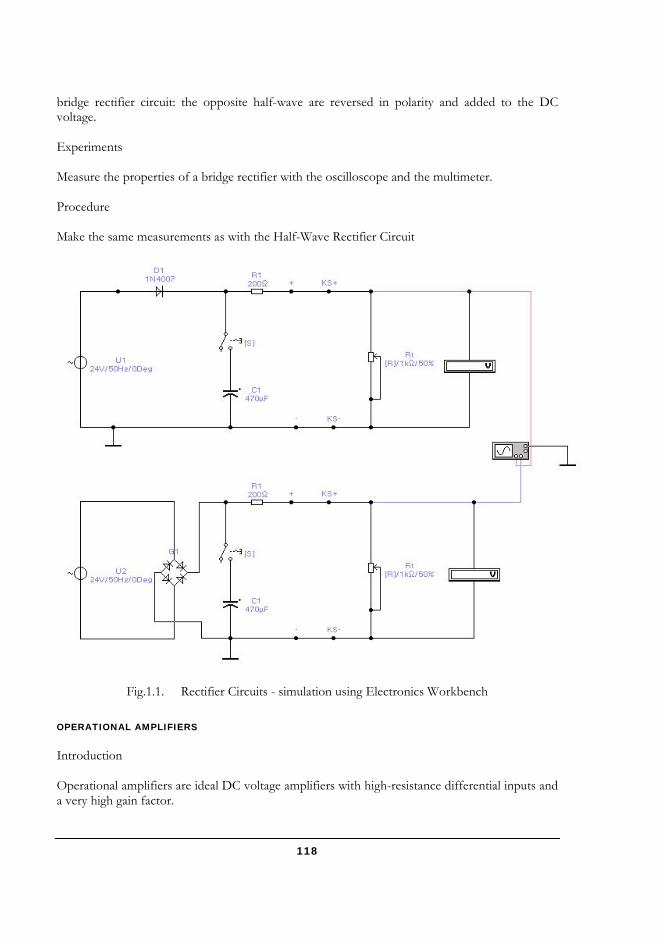
bridge rectifier circuit: the opposite half-wave are reversed in polarity and added to the DC voltage. Experiments Measure the properties of a bridge rectifier with the oscilloscope and the multimeter. Procedure Make the same measurements as with the Half-Wave Rectifier Circuit
Fig.1.1. Rectifier Circuits - simulation using Electronics Workbench OPERATIONAL AMPLIFIERS Introduction Operational amplifiers are ideal DC voltage amplifiers with high-resistance differential inputs and a very high gain factor.
118

Operational amplifiers are available as integrated standard components (e.g. μA741). The following experiments are designed to examine the basic properties of these components.
Operating Amplifier as Inverting Amplifier
Inverting amplifiers are circuit arrangements in which the input voltage is inverted at the output. With AC voltage there is a phase shift of 1800 between the input and output voltages. An
Fig.1.2. Record of the output voltages with the Electronics Workbench oscilloscope
inverting amplifier can be used to amplify or to reduce the input signal according to the size of resistors R2 and R1.
Gain factor : A = -R2/R1 => Uiz = -R27R1*Uul1
Experiments
Measure the properties of an inverting amplifier with the oscilloscope and the multimeter.
Procedure
119

Set up the circuit according to Fig.2.1. with the support of Electronics Workbench. Then record output voltages with the oscilloscope and transfer their curve shape onto the diagram. Then do the same measurement on the electronic module and compare the results.
Operating Amplifier as Non-Inverting Amplifier
In non-inverting amplifiers, input and output voltage have the same polarity; the phase shift with AC voltage is 00.
Gain factor: A = 1 + R2/R1 => Uiz = (1+R2/R1)*Uul1
Experiments
Measure the properties of an inverting amplifier with the oscilloscope and the multimeter.
Procedure
Make the same measurements as with the Inverting Amplifier
Fig.2. Operational amplifiers
120

Fig.2.1. Operational Amplifiers - simulation using Electronics Workbench
Fig.2.2. Record the output voltages with the Electronics Workbench oscilloscope
121

Fig.2.3. Record the output voltages on Electronic module
122

RCS - Robot Control Systems
Laboratory 1
Robots - general structure - components - features
1. Aim The purpose of this paper is to familiarize students with the concept of robot functioning, applications, components (joints, motors, sensors) thereof.
2. Proceedings
In carrying out the work it will be taken into account that there are different types of robots, different classes, different applications and different structures.
Fig. 1. a) industrial robot
b) mobile robot (proximity sensors); c) toy robot
123

3. Conducting work
Students will choose one type of robot and seek the Internet using search engines, information about it; The documentation made will take into account the following elements: - the use of the robot; - type / class robot; - structure; - components (types, operation): - sensors / transducers - motors / actuators - joints - user. 4. Issues Make a PowerPoint presentation and a written report describing the operation of a robot, components, fittings, sensors and applications of this robot.
124

Summer school of robotics exercises
Automated garage door Design an automated system of opening/closing the garage door using Robopro- Fischertechnik. The door is opened by the I1 entrance key (remote control). At the upper side, the door has got an I2 on switch, which shows that the door has been opened, while at the lower side, there is an I3 on switch showing that the door has been closed. When the door is completely open, it is necessary to keep it open for 10 seconds and then the door will be automatically closed. There is an optical sensor built in the door-case, which prevents the closing of the door in case there is someone underneath.
By interrupting the optical sensor beam, the door is automatically lifted to the upper end position and is kept in this position for 10 seconds after which it is automatically lowered!
In the garage there is an I5 key which makes it possible to keep the garage door open while cleaning it and by pressing the key again, the door is closed!
While opening/closing the door warning lights blink as well as messages appearing on the PC monitor.
125

Operational amplifiers
In this exercise we will review the operational amplifier μA741, make an expression for the amplification (closed-loop A), and record the input and output signals of the operational amplifier with an oscilloscope according to the following schematics! Materials and instruments: NI myDAQ Program Multisim 12.0 Experimental board 4 1/4W resistors (1k1;10k;100k;1MΩ) Trimmer potentiometer 10 kΩ x 2 Operational amplifier μA741 Set of counductors Draw the schematics of the non-invertive operational amplifier in NI MULTISIM 12.0! Use the specific ANALOG/ANALOG_VIRTUAL/OPAM_3T_VIRTUAL operational amplifier and SOURCES/POWER_SOURCES/AC_POWER AC voltage source blocks. Set the frequency to 100 Hz sinusoidal and the peak voltage to 0.5 V. Connect the TETRONIX oscilloscope to the amp output (TEST_PT1) and make a SCREEN SHOT for trimmer positions 0% and 100% as seen in the figure. Set the oscilloscope according to the figure from which is visible that the maximal amplification is Closed-loop A=10. Excerpt an expression for the closed-loop amplification A depending on the feedback factor β. The operational amplifier has a gain bandwidth product of GPB=1 MHz, meaning that the product of the throughput frequency range and the open loop gain Av=1Mhz, that means that with a higher amplification comes a lower throughput range. Try to set the input frequency to 1kHz, and then to 100kHz!
126

Since we set the ideal operational amplifier in NI Multisim, does the amplification change with the input frequency?
Write down your observations and excerpt an expression for the amplification A:
Connect the elements of the circuit according to the schematics on the experimental board! Keep in mind to connect the power supply for the OA (note that the +15V goes to pin 7, and the -15V to pin 4).
127

On the left figure there is the pin layout of the OA μA741. On the right is the offset calibration (when the input voltage is zero – short circuited input – then the output voltage must be zero).
Using the function generator and NI ELVISmx instrument launcher (FGEN) you will get the input voltage V1 (100 Hz signal, 0.02 Vpp). On the non-invertive input of the OA (pin 3) connect AO 0. Connect AGDN to ground (GND). Between pins 1 and 5 OA connect a 10kOhm trimmer potentiometer so that the slider is connected to -15V according to the schematics on the right. Set the R1=1MOhm resistor in the feedback loop. Open the oscilloscope (SCOPE) and set Scope CH0 AI0 to the input of the OA (pin 3), and observe the amplified signal on the output of the OA (pin 6) (Scope CH1 AI1). Change the FGEN frequency from 100Hz to 10kHz and record SCREEN SHOT for 100Hz, 1kHz and 10kHz! Check the output amplification in decibels (A=20log Vout/Vin), and check the phase shift (how much is the output signal late compared to the input signal in degrees). Express your observations :
Compare your results with the Bode's diagrams given in the figures for all listed frequency settings.
128

R1=1Mohm GBW=1 Mhz A=1+1000k/1k1=910 fg=1000k/910=1,098 kHz R1=100k GBW=1 Mhz Av=1+100k/1k1=91,9 fg=1000k/91=10,88 kHz
Write down the measurements in the table!
Feedback
resistance R1
10 kΩ
100 kΩ
1 MΩ
100 Hz
1 kHz
10 kHz
100 Hz
1 kHz
10 kHz
100 Hz
1 kHz
10 kHz
Gain A(x)
Gain A(dB)
Phase shift φ(º)
129
Bode's diagrams given in the figures can be recorded by connecting AO 0 and AO 0+ on the non-invertive input of the OA (pin 3), AI1+ to the output of the OA (pin 6), and the AGND, AI0- and AI1- signals to the GND on the experimental board. Using the NI ELVISmx instrument launcher (BODE) you will get an amplitudal-phase-frequency diagram called Bode's diagram where the amplification, output phase shift and the upper peak frequency, which is for a feedback resistance of R1=100kOhm 10.88 kHz, are nicely visible in a logarithmical measure. You can check this with a cursor. Set the Bode analyzer like this: Start frequency 100 Hz Stop frequency 20 kHz 5 steps per decade Peak 0,01V Press the run icon and wait for the PC to draw Bode's diagrams for the non-invertive operational amplifier. You can use the cursor to measure the upper peak frequency of the OA fu. That's the frequency where the amplification drops for 3 dB compared to DC signals, that is to 70.7%. Check the signal phase, too. What's the output phase shift at the upper peak frequency? Determine the slope of the amplitude characteristics from Bode's diagram in dB/sec! Explain what does a decade mean in Bode's diagrams and why are the characteristics drawn in a log-log measure? Express your observations :
130

Microphone preamplifiers In the figure there are schematics of an non-invertive OA with a capacitive microphone connected to its input. Materials and instruments: NI myDAQ Program Multisim 12.0 Experimental board 4 1/4W resistors (1k1 x 2;10k x 2;100k) Trimmer potentiometer 10 kΩ Capacitor 10 μF Operational amplifier μA741 x 2 Capacitive microphone Speaker Set of conductors The microphone (red conductor) is powered through the R2=10kOhm resistor connected to +15V. The signal we need to amplify is taken through the C1=10μF capacitor and is lead to the non-invertive input of the OA (excerpt 3). The capacitor is used to separate the directional voltage component, and lets through to the amp only the useful alternating signal that we need to amplify, the resistor is used to receive the input voltage on the non-invertive inout, and together they make a filter of low permeability. We get the lower peak frequency from the amplification expression, that is when the amplification on the CR output falls for 3 dB compared to the input. fl= 1/(2πR1C1) and in this case it is equal to fd=1/(2π*1k1*10μF)=14,47 Hz! How do we get to the amplification and lower peak frequency expressions? Our CR input network looks like this:
Output voltage expression
Vout=Vin*R1/(Xc+R1).
From which you get the amplification expression A=Vout/Vin. A=R1/(1/j ωC1+R1) deriving this equation... A=1/(1+1/j ωR1C1) If 1/(R1C1) is the lower peak frequency ωd we get: A=1/(1-j ωd/ ω) We get the amplification in dB like this: A(dB)= 20 log A that is when ω= ωd A(dB)=20 log( ) = - 3 dB
131

R11.1kΩ
R210kΩ
R3
100kΩR41.1kΩ
C1
10µF
MIC
15V
-15V
U17413
2
4
7
6
51
VSS
1
0 0
0
4
VDD
2
3
The amplification of the non-invertive OA is determined only by outer elements, that is the resistance ratio as follows: A=1+R3/R4
A= 1+100k/1k1 giving us amplification of about 92 times or about 39 dB.
The upper peak frequency of the preamp fu is determined by the characteristics of the OA itself (bandwith=1MHz). Dividing that with the amplification 92 we get the upper peak frequency of 10.87 kHz.
Microphone preamp
Connect the elements according to the schematics. Make sure that the plus pole of the capacitive microphone (red conductor) is connected to the plus of the capacitor, and then place a 10kOhm resistor int hat node and tie it ti +15V. Try the preamp out and see how it works. Start NI ELVISmx. Start the oscilloscope. Choose two channels. Connect the AI0+ and AI1+ inputs to OA pins 2 and 6, respectively. Connect the AI0- and AI1- inputs to minus (blue line) on the left side of the experimental board. Set the oscilloscope and press RUN.
You will notice that the output is amplified multiple times compared to the input. You probably notice that the output is shifted to plus for about 100mV. Set the drift to zero like described in exercise 4 or simply connect the trimmer 10kOhm between 1 and 5, the slider to -15V and set the signal on channel 2 to 0V. Test the preamplifier with different sounds. Set the time base to 1ms and try again.
132

Microphone signal (CH0) and OA output signal (CH1)
133
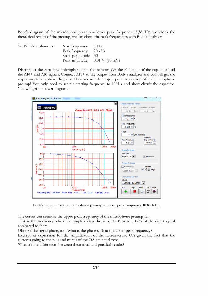
Bode's diagram of the microphone preamp – lower peak frequency 15,85 Hz. To check the theoretical results of the preamp, we can check the peak frequencies with Bode's analyser
Set Bode's analyser to : Start frequency 1 Hz Peak frequency 20 kHz Steps per decade 30 Peak amplitude 0,01 V (10 mV)
Disconnect the capacitive microphone and the resistor. On the plus pole of the capacitor lead the AI0+ and AI0 signals. Connect AI1+ to the output! Run Bode's analyzer and you will get the upper amplitude-phase diagram. Now record the upper peak frequency of the microphone preamp! You only need to set the starting frequency to 100Hz and short circuit the capacitor. You will get the lower diagram.
Bode's diagram of the microphone preamp – upper peak frequency 10,85 kHz
The cursor can measure the upper peak frequency of the microphone preamp fu. That is the frequency where the amplification drops by 3 dB or to 70.7% of the direct signal compared to them. Observe the signal phase, too! What is the phase shift at the upper peak frequency? Excerpt an expression for the amplification of the non-invertive OA given the fact that the currents going to the plus and minus of the OA are equal zero. What are the differences between theoretical and practical results?
134

Express your observations :
Using the FGEN function generator we will generate a 2kHz signal and connect it to a speaker. Given the fact that the analogue output of NI myDAQ isn't capable of outputting a strong enough current for a 50 Ohm speaker, we will make a voltage follower with the OA, connecting its output to the speaker. Now the analogue output AO0 is loaded with the 10kOhm resistor, and the OA with the 50Ohm resistance. It is on the following figure.
135
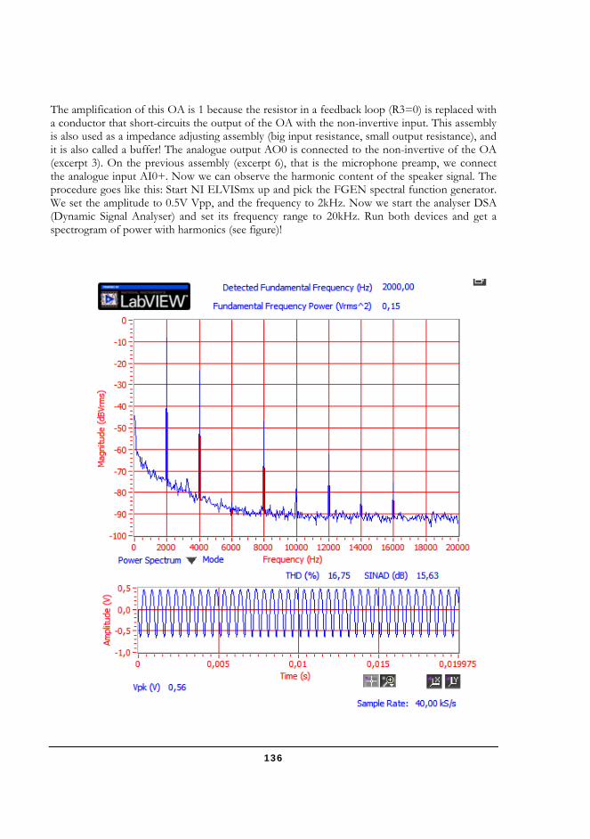
The amplification of this OA is 1 because the resistor in a feedback loop (R3=0) is replaced with a conductor that short-circuits the output of the OA with the non-invertive input. This assembly is also used as a impedance adjusting assembly (big input resistance, small output resistance), and it is also called a buffer! The analogue output AO0 is connected to the non-invertive of the OA (excerpt 3). On the previous assembly (excerpt 6), that is the microphone preamp, we connect the analogue input AI0+. Now we can observe the harmonic content of the speaker signal. The procedure goes like this: Start NI ELVISmx up and pick the FGEN spectral function generator. We set the amplitude to 0.5V Vpp, and the frequency to 2kHz. Now we start the analyser DSA (Dynamic Signal Analyser) and set its frequency range to 20kHz. Run both devices and get a spectrogram of power with harmonics (see figure)!
136

Voltage splitter
In this exercise we will review a voltage splitter and voltage calculations on it. We will see how it works given the load! Materials and instruments: NI myDAQ Experimental board 4 1/4W resistors 4k7 Trimmer potentiometer 10 kΩ Operational amplifier μA 741 Set of conductors Connect the elements according to the schematics to get a voltage splitter. Because we're using equal resistors it is the assumption that both will have the same voltage.
Check the resistors so that you measure every resistor by itself with a special virtual instrument DMM. Connect the resistors according to the schematics to the voltage source +15V and AGND. Using a digital multimeter measure the voltages on each resistor and the current going through them. Excerpt the expression for the output voltage Vout (using general numbers), calculate Vout and compare it to the measurements. Express your observations :
137
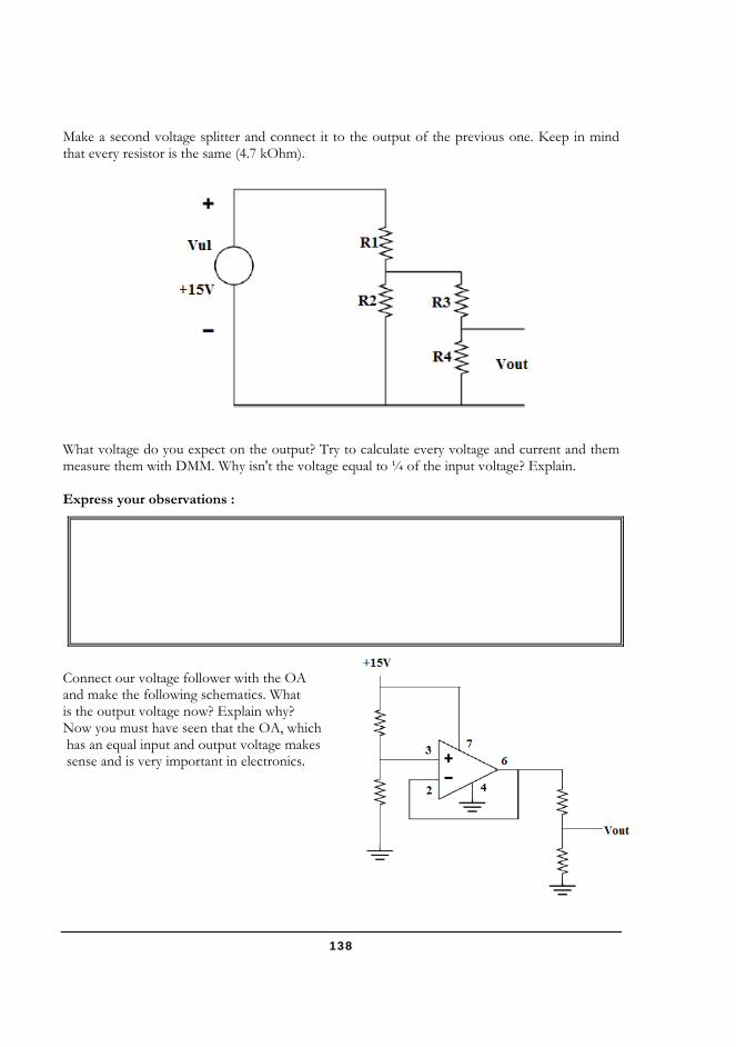
Make a second voltage splitter and connect it to the output of the previous one. Keep in mind that every resistor is the same (4.7 kOhm).
What voltage do you expect on the output? Try to calculate every voltage and current and them measure them with DMM. Why isn't the voltage equal to ¼ of the input voltage? Explain.
Express your observations :
Connect our voltage follower with the OA and make the following schematics. What is the output voltage now? Explain why? Now you must have seen that the OA, which has an equal input and output voltage makes sense and is very important in electronics.
138
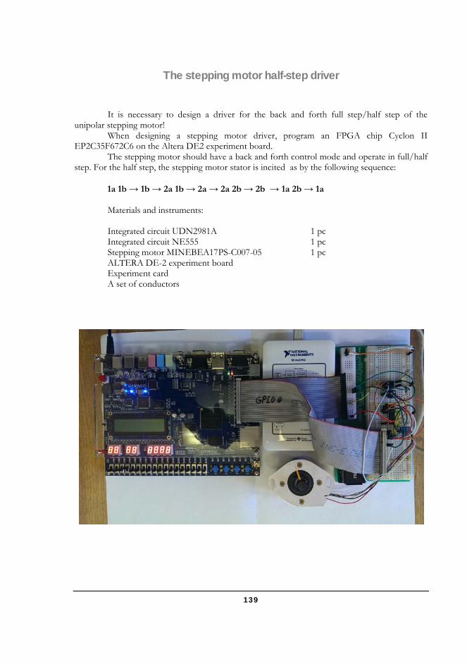
The stepping motor half-step driver
It is necessary to design a driver for the back and forth full step/half step of the unipolar stepping motor!
When designing a stepping motor driver, program an FPGA chip Cyclon II EP2C35F672C6 on the Altera DE2 experiment board.
The stepping motor should have a back and forth control mode and operate in full/half step. For the half step, the stepping motor stator is incited as by the following sequence: 1a 1b → 1b → 2a 1b → 2a → 2a 2b → 2b → 1a 2b → 1a
Materials and instruments: Integrated circuit UDN2981A 1 pc Integrated circuit NE555 1 pc Stepping motor MINEBEA17PS-C007-05 1 pc ALTERA DE-2 experiment board Experiment card A set of conductors
139
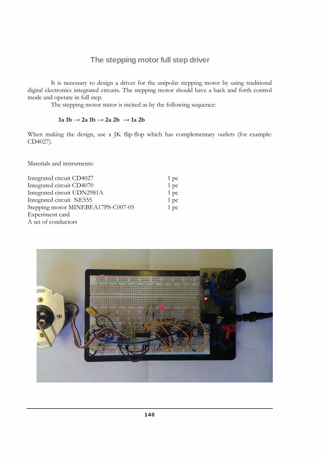
The stepping motor full step driver
It is necessary to design a driver for the unipolar stepping motor by using traditional digital electronics integrated circuits. The stepping motor should have a back and forth control mode and operate in full step. The stepping motor stator is incited as by the following sequence: 1a 1b → 2a 1b → 2a 2b → 1a 2b When making the design, use a JK flip-flop which has complementary outlets (for example: CD4027). Materials and instruments: Integrated circuit CD4027 1 pc Integrated circuit CD4070 1 pc Integrated circuit UDN2981A 1 pc Integrated circuit NE555 1 pc Stepping motor MINEBEA17PS-C007-05 1 pc Experiment card A set of conductors
140

4 x 3 phone dial scanning This task will teach you how to use the 8-bit port NImyDAQ in order to detect the phone dial keys arranged into a 4 x 3 matrix (4 rows, 3 columns). The Labview program detects the pressed key and turns into a 7-bit code which contains the row and column address of the pressed key. The 7-bit code is transformed into a Nybble that contains the information about the pressed key, which is then illuminated on the phone dial (PC monitor). Materials and instruments: NI my DAQ 4 x 3 phone dial experiment card a set of conductors
141