Embed Size (px)
Citation preview

Subscriber access provided by Caltech Library Services
Nano Letters is published by the American Chemical Society. 1155 SixteenthStreet N.W., Washington, DC 20036
Letter
Electrooptic Modulation in Thin FilmBarium Titanate Plasmonic InterferometersMatthew J. Dicken, Luke A. Sweatlock, Domenico Pacifici,
Henri J. Lezec, Kaushik Bhattacharya, and Harry A. AtwaterNano Lett., 2008, 8 (11), 4048-4052• DOI: 10.1021/nl802981q • Publication Date (Web): 11 October 2008
Downloaded from http://pubs.acs.org on April 16, 2009
More About This Article
Additional resources and features associated with this article are available within the HTML version:
• Supporting Information• Access to high resolution figures• Links to articles and content related to this article• Copyright permission to reproduce figures and/or text from this article

Electrooptic Modulation in Thin FilmBarium Titanate PlasmonicInterferometersMatthew J. Dicken,† Luke A. Sweatlock,‡ Domenico Pacifici,† Henri J. Lezec,§Kaushik Bhattacharya,† and Harry A. Atwater*,†
Applied Physics, California Institute of Technology, Pasadena, California 91125,Northrop Grumman Space Technology, Redondo Beach, California 90278, and Centerfor Nanoscale Science and Technology, National Insitiute of Standards andTechnology, Gaithersburg, Maryland 20899
Received October 1, 2008
ABSTRACT
We demonstrate control of the surface plasmon polariton wavevector in an active metal-dielectric plasmonic interferometer by utilizingelectrooptic barium titanate as the dielectric layer. Arrays of subwavelength interferometers were fabricated from pairs of parallel slits milledin silver on barium titanate thin films. Plasmon-mediated transmission of incident light through the subwavelength slits is modulated by anexternal voltage applied across the barium titanate thin film. Transmitted light modulation is ascribed to two effects, electrically induceddomain switching and electrooptic modulation of the barium titanate index.
The optical transmittance of arrays of subwavelength surfaceapertures in metal films, such as holes and slits, has generatedenormous scientific interest, and surface plasmons have beenfound to play a governing role.1-5 Surface apertures havebeen studied extensively as a means for coupling electro-magnetic waves into and out of surface plasmon polariton(SPP) modes. Recently, passive plasmonic interferometerswere constructed from pairs of slits as a means to enhanceunderstanding of slit array transmittance.6 Although at presentthese devices are only prototypical, ultracompact modulatorsderived from subwavelength slit arrays could have activeareas less than 10 µm2, compared to 1000 µm2 for conven-tional electrooptic modulators.
SPPs are highly confined electromagnetic waves thatpropagate along a metal-dielectric interface by coupling toa polarization of the electron gas in the metal. Light can becoupled into and out of these modes by scattering from abruptstructural features such as grooves or slits.7 The groundworkfor passive plasmonic structures has been laid throughintensive studies of SPP propagation in metal-dielectricstructures.8 It has been shown that these waves can interactwith light transmitted through slits to create an interferencepattern in the overall transmission intensity and this interfer-ence pattern can be affected by changes to the imaginary
part of the SPP wavevector.9 SPP modulation via theelectrooptic effect has been studied previously in polymerfilms by coupling light into surface plasmon modes at ametal-polymer interface.10 Here, we investigate dynamicmodulation of the real part of the SPP wavevector byreplacing the “dielectric” layer in the structure with anelectrooptically active barium titanate thin solid film.
Barium titanate is a well-known perovskite ferroelectricmaterial that exhibits a large electrooptic coefficient, on theorder of r ) 100 pm/V, and large birefringence due to itsatomic structure, ∆n ) 0.05.11,12 Thin films of barium titanateare deposited by numerous techniques, and their opticalproperties have been widely investigated and employed inelectrooptic waveguides and modulators.13-15 Barium titanatehas a tetragonal crystal structure with an ordinary index, no
) 2.412, corresponding to the shorter a-axis, which is largerthan the extraordinary index, ne ) 2.36, along the c-axis.Ferroelectric domains form when the film is cooled belowthe Curie temperature (∼120 °C) and their final orientationis affected by film stresses, as well as lattice and thermalexpansion mismatch. Ferroelectric domains in barium titanatecan be characterized by their orientation in-plane (a-axis)or out-of-plane (c-axis). Barium titanate thin films depositedon oxide thin film electrodes have been characterized bypiezoresponse force microscopy and show both in-plane andout-of-plane domains.16 These domains can be manipulatedby applying an electric field across the material, and in-planedomains can be forced to switch out-of-plane under an
* Corresponding author.† California Institute of Technology.‡ Northrop Grumman Space Technology.§ Center for Nanoscale Science and Technology.
NANOLETTERS
2008Vol. 8, No. 11
4048-4052
10.1021/nl802981q CCC: $40.75 2008 American Chemical SocietyPublished on Web 10/11/2008

applied field greater than the coercive field. This domainswitching event is accompanied by a large change in theindex of the barium titanate thin film due to the birefringencein the material. Using barium titanate thin films, we modulatethe real part of the index of refraction at the Ag/BaTiO3
interface and thereby modulate the SPP wavevector.Discussion. A schematic of the plasmonic interferometer
based on double-slit transmission and electrooptic modulationof the SPP wavevector is shown in Figure 1. The opticallyactive oxide thin film stack used for these SPP mediateddouble-slit interferometers was deposited without breakingvacuum in a pulsed laser deposition system (Neocera 180).Strontium ruthenate and barium titanate thin films weredeposited on double-side polished magnesium oxide sub-strates (MTI Crystal). MgO substrates with dimensions 10mm × 10 mm × 0.5 mm were attached to a molybdenumholder with silver paste for good thermal contact. Substrateswere annealed at 900 °C for 1 h in vacuum (P ) 1 × 10⁻⁷
Torr) prior to growth. The SrRuO3 and BaTiO3 films weredeposited at 700 °C with background oxygen partial pressuresPO2 ) 150 mTorr and PO2 ) 10 mTorr, respectively. Thesubstrates were rotated 60 deg/s, and the target-substratedistance was kept at 9 cm during growth. A KrF excimerlaser (λ ) 248 nm) focused onto sintered targets of 99.9%pure SrRuO3 and 99.99% pure BaTiO3 was used to ablatethe material at a pulse rate of 10 Hz with a pulse power of300 mJ. After deposition, the films were cooled to roomtemperature at a rate of 5 deg/min at PO2 ) 1 Torr. The filmthicknesses grown under these conditions were 400 nmbarium titanate and 200 nm strontium ruthenate. The crystalstructure of the samples was characterized by X-ray diffrac-tion and reflection high-energy electron diffraction (RHEED).θ-2θ X-ray scans were performed in a Panalytical X’PERTdiffractometer using Cu KR radiation (λ ) 1.5406 Å). θ-2θX-ray scans show the epitaxial, single-crystalline phase (100/001), of the BaTiO3/SrRuO3/MgO structure. RHEED wasperformed ex situ in a separate chamber equipped with a 25keV electron gun. Silver (300 nm) and chromium (30 nm)films were vacuum deposited by evaporation onto the samplethrough a shadow mask to expose only a rectangular areaon the sample. The structures consist of pairs of parallel slitsetched into the metal layer by FIB milling (FEI Nova 600dual beam focused ion beam system, Ga+ ions, 30 keV).
The slits are 5 µm long by 100 nm wide with slit pitchstarting at 500 nm and increasing by 20 nm for each devicealong a row. Each device is laterally separated by 5 µm(Figure 2). Electrical contacts are made to the strontiumruthenate film by mechanically etching the barium titanatefilm and contacting the strontium ruthenate using conven-tional silver paste. The final device is mounted onto a glassslide, and copper tape is used to contact the top chromium/silver layer and bottom strontium ruthenate layer. A total of240 plasmonic interferometers were investigated using thesemethods.
The device array is illuminated by a TM-polarized (H fieldparallel to the long axis of the slit) light source causing afraction of the energy to be coupled into SPP modes at theAg/BaTiO3 interface and the remaining to be transmitted orreflected. The SPP mode extends evanescently into both themetal and ferroelectric films, and the SPP wavevector, kSPP,is determined by the optical properties of both layers. Thetwo counterpropagating surface waves are scattered out fromthe interface into radiative modes at the opposite slit. TheSPPs interfere with the transmitted light at each slit corre-sponding to their phase accumulation during propagationalong the interface. Interference with the transmitted lightcan be modulated by changing the SPP phase via slit pitchor SPP wavevector. We designed experiments, comple-mented by full field electromagnetic simulations, based onplanar arrays of these devices (Figure 2) to investigate opticalmodulation in SPP-mediated double-slit interferometers.
A simple analytical treatment of the total transmittedintensity resulting from interference between the incidentfield and the SPP field can be used to show that smallchanges in the index of refraction of the dielectric layer can
Figure 1. Schematic of a plasmonic modulator based on interferenceof SPPs launched from a set of parallel slits milled into a planarmetal film. The counterpropagating SPPs travel with wavevectorkSPP along the Ag/BaTiO3 interface. The interference of these SPPswith the transmitted fields can be affected by an applied voltageacross the BaTiO3 layer, by means of electrooptic modulation andelectrically induced domain switching.
Figure 2. Double-slit SPP interferometer array. CCD image,collected with a 10× objective, of an array of double-slit devicespatterned in Cr/Ag on BaTiO3 illuminated by TM-polarized (H-field parallel to the long axis of the slit) 688 nm laser light. Theslit pitch starts at 0.50 µm and increases by 20 nm for each devicealong a row. The observed intensity oscillation as a function of slitpitch is due to SPP interference with light transmitted through eachslit. Insets: Scanning electron micrograph of slit pairs milled byfocused ion beam in a chromium on silver layer. 50× image ofdevices with slit pitches varying from 1.50 to 1.98 µm showingone full period of transmitted intensity oscillation.
Nano Lett., Vol. 8, No. 11, 2008 4049

lead to significant changes in the transmitted intensity profile.For this work, the double-slit device is governed by plasmoninterference at the bottom interface of the Ag, due to thehighly absorbing chromium layer at the top surface. Con-sidering the transmission at each slit to be the sum of atransmitted field and a SPP field that has acquired somephase, φ ) kSPPx + φo, the resulting normalized transmittedintensity can be expressed as17
IT
Io) 1+ (�o�o′)
2e-Rx + 2��o′e-(R/2)x cos[kSPPx+ φo] (1)
where �o and �o′ are scattering efficiencies for SPP couplingat each slit, R is the absorption coefficient, kSPP is the SPPwavevector, and φo is the phase imparted by scattering fromthe slit. Data from experiments and full field electromagneticsimulations have been fit by this model to extract the relativeindex change of the active barium titanate layer from
nSPP ) √εAgεEff /(εAg + εEff)
where εEff is an effective dielectric constant describing theproperties of all nonmetallic layers.18
To explore the physics of this double-slit device, simula-tions were performed using full field finite-difference time-domain software (FDTD).19 A multioscillator Lorentz-Drudemodel is used for the chromium and silver layers withparameters given by Rakic et al.20 The barium titanate andstrontium ruthenate complex refractive index data werederived from variable-angle spectroscopic ellipsometry mea-surements.21 Figure 3a shows the magnetic field profile (Hy)for one device with a slit pitch of 1.50 µm and an index ofrefraction, nBTO, of 2.20 for the barium titanate layer. Theinput plane wave (λ ) 688 nm) from Z ) 1 µm is transmittedthrough the 100 nm wide slits, and a fraction is scatteredinto surface plasmon polariton modes propagating along theAg/BaTiO3 interface to the left and right of each slit.Counterpropagating SPPs along the interferometer armformed between the slits interfere constructively or destruc-tively depending on slit pitch and SPP wavevector. Figure3b shows the absolute magnetic field (Hy
2) from the samesimulation. The resonant mode formed by the two counter-propagating SPPs inside the cavity can be identified in thisfigure. SPPs propagating away from each slit appear in theform of a continuously decaying intensity profile along theAg/BaTiO3 interface. Figure 3b also shows fields beingcoupled into a waveguide mode formed by the 400 nmbarium titanate film.
At each slit, a fraction of the incoming energy scattersout of the SPP mode and interferes with the transmitted lightto create an overall modulation in the transmitted power.The optical power flow through the device can be analyzedfor these simulations by plotting the Poynting vector (Sz)(Figure 3c). A monitor line placed along the bottom of thesimulation (Z ) -1 µm) can be used to monitor the net“transmission”, that is, the power flow away from the slitpair in the -z direction. Plotting the integrated power flowout of the device for each slit pitch yields an interferencepattern as predicted from theory (Figure 4a). Simulationswere done for these devices using input barium titanateindices of refraction of 2.20 and 2.21 to approximate the
index change under applied bias. The range of indicessimulated is indicative of a change in index due to somedegree of a-domain to c-domain switching under bias. TheseFDTD data were fit using eq 1 to extract nSPP and nEff
following from εEff ) nEff2. We find that comparing simula-
tions with nBTO ) 2.20 and 2.21, the model fit yields nSPP )2.626 and 2.646 from which nEff ) 2.24 and 2.25, respec-tively, corresponding to a change ∆nEff ) 0.01 (Figure 4a).The difference in nEff from the input nBTO is due to SPPinteraction with the entire material stack beneath the bariumtitanate, which is naturally addressed in the FDTD simulation,but not the analytical model. This does not affect the overallchange in index, both the input and simulated index changeare ∆n ) 0.01. It is important to note that the intensity ofthe modulation is indicative of the change in nSPP for a givenslit pitch and material index and can be used to put a lowerlimit on the index change for a given device. The percentchange in integrated power flow for each device, as nBTO ischanged from 2.20 to 2.21, is plotted in Figure 4b. We caninfer that the smallest change in nEff to yield 15% modulationfor a device with pitch 2.26 µm with the optical materialproperties simulated here is ∆nEff ) 0.01.
We fabricated an array of double-slit interferometerstructures in silver on barium titanate (Figure 2). The double-slit device array was illuminated from the topside, normalto the sample, with a TM-polarized (λ ) 688 nm) diode lasersource. The diode laser was aligned to the optical axis of aZeiss Axiovert 135 inverted microscope using a quartz cube
Figure 3. FDTD device simulations. Full-field finite difference timedomain simulations of a double-slit SPP interferometer device witha slit pitch of 1.50 µm illuminated by λ ) 688 nm plane-wavelight. (a) Magnetic field (Hy) distribution for the device structureshowing the destructive interference of the counterpropagating SPPsbetween the slits. (b) Absolute magnetic field (Hy
2) showing thestanding wave mode formed by the counterpropagating SPPs aswell as the slowly decaying SPPs propagating away from each slit.(c) Power flow (Sz) simulation used to quantify the relative powerleaving the modeled devices at position Z ) -1 along the Xposition.
4050 Nano Lett., Vol. 8, No. 11, 2008
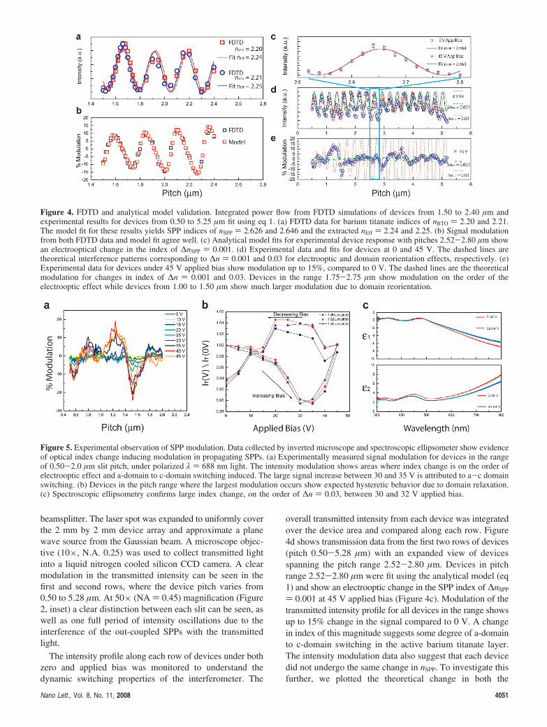
beamsplitter. The laser spot was expanded to uniformly coverthe 2 mm by 2 mm device array and approximate a planewave source from the Gaussian beam. A microscope objec-tive (10×, N.A. 0.25) was used to collect transmitted lightinto a liquid nitrogen cooled silicon CCD camera. A clearmodulation in the transmitted intensity can be seen in thefirst and second rows, where the device pitch varies from0.50 to 5.28 µm. At 50× (NA ) 0.45) magnification (Figure2, inset) a clear distinction between each slit can be seen, aswell as one full period of intensity oscillations due to theinterference of the out-coupled SPPs with the transmittedlight.
The intensity profile along each row of devices under bothzero and applied bias was monitored to understand thedynamic switching properties of the interferometer. The
overall transmitted intensity from each device was integratedover the device area and compared along each row. Figure4d shows transmission data from the first two rows of devices(pitch 0.50-5.28 µm) with an expanded view of devicesspanning the pitch range 2.52-2.80 µm. Devices in pitchrange 2.52-2.80 µm were fit using the analytical model (eq1) and show an electrooptic change in the SPP index of ∆nSPP
) 0.001 at 45 V applied bias (Figure 4c). Modulation of thetransmitted intensity profile for all devices in the range showsup to 15% change in the signal compared to 0 V. A changein index of this magnitude suggests some degree of a-domainto c-domain switching in the active barium titanate layer.The intensity modulation data also suggest that each devicedid not undergo the same change in nSPP. To investigate thisfurther, we plotted the theoretical change in both the
Figure 4. FDTD and analytical model validation. Integrated power flow from FDTD simulations of devices from 1.50 to 2.40 µm andexperimental results for devices from 0.50 to 5.25 µm fit using eq 1. (a) FDTD data for barium titanate indices of nBTO ) 2.20 and 2.21.The model fit for these results yields SPP indices of nSPP ) 2.626 and 2.646 and the extracted nEff ) 2.24 and 2.25. (b) Signal modulationfrom both FDTD data and model fit agree well. (c) Analytical model fits for experimental device response with pitches 2.52-2.80 µm showan electrooptical change in the index of ∆nSPP ) 0.001. (d) Experimental data and fits for devices at 0 and 45 V. The dashed lines aretheoretical interference patterns corresponding to ∆n ) 0.001 and 0.03 for electrooptic and domain reorientation effects, respectively. (e)Experimental data for devices under 45 V applied bias show modulation up to 15%, compared to 0 V. The dashed lines are the theoreticalmodulation for changes in index of ∆n ) 0.001 and 0.03. Devices in the range 1.75-2.75 µm show modulation on the order of theelectrooptic effect while devices from 1.00 to 1.50 µm show much larger modulation due to domain reorientation.
Figure 5. Experimental observation of SPP modulation. Data collected by inverted microscope and spectroscopic ellipsometer show evidenceof optical index change inducing modulation in propagating SPPs. (a) Experimentally measured signal modulation for devices in the rangeof 0.50-2.0 µm slit pitch, under polarized λ ) 688 nm light. The intensity modulation shows areas where index change is on the order ofelectrooptic effect and a-domain to c-domain switching induced. The large signal increase between 30 and 35 V is attributed to a-c domainswitching. (b) Devices in the pitch range where the largest modulation occurs show expected hysteretic behavior due to domain relaxation.(c) Spectroscopic ellipsometry confirms large index change, on the order of ∆n ) 0.03, between 30 and 32 V applied bias.
Nano Lett., Vol. 8, No. 11, 2008 4051

interference pattern and the percent modulation approximat-ing electrooptic switching (∆neo ) 0.001) and domainswitching (∆na-c ) 0.03) effects (Figure 4e). We alsoobserved that in some regions the device transmittancedeparted from the prediction of the analytic model due tolocal changes in nEff arising from changes in either the Ag/BaTiO3 index or local film inhomogeneities. Intensity datawere compiled in 5 V increments from 0 to 45 V and thepercent change in intensity compared to 0 V is plotted inFigure 5a. We see a reasonable comparison of the modulationdata for devices with pitches in the range 0.50-1.00 µmwith theoretical modulation due to electrical modulation ofthe SPP wavevector, via domain switching effects on theorder of ∆nEff ) 0.03. For slit pitches less than 1.00 µm, themaxima and minima of the intensity modulation correspondwell with the inflection points of the 0 V interference pattern.This implies that the change in index from device to devicewas similar in this range. Devices between 1.00 and 1.80µm slit pitch show the largest change in intensity modulation.By comparing the data in this range to the percentagemodulation of the analytical model, we can put a lower limitof ∆nEff ) 0.03 on the index change in these devices. Thislarger effect is attributed to domain switching or piezoelectricactivity in the barium titanate film, such that devices showingvery large intensity modulation are undergoing 90° domainswitching from c-axis in-plane to c-axis out-of-plane.16 Thiseffect would yield a change in the index of refraction on theorder of the birefringence of the material, ∆n ) 0.05. Thefraction of domains that switch between the slits of eachdevice will dictate the change in effective index for thedevice.
To investigate this further, the bias across the devices wascycled from 0 to 45 to 0 V. A plot of the response of threedevices (1.60, 1.62, 1.64 µm slit pitch) to the voltage cycleis shown in Figure 5b. The intensities of these devices werenormalized to their values at 0 V. The device response showshysteresis demonstrative of ferroelectric domain switching.As the bias is increased, devices in this range show a decreasein output intensity as the index changed up to 35 V, and thefollowing increase in intensity suggests that the index changewas sufficient to move the response through a minimum inthe interference pattern. As the bias is decreased, the domainsthat have switched from c-axis in-plane to c-axis out-of-planerelax slowly to their original state. At 15 V, decreasing bias,the index begins to follow the same path through the intensityminimum.
Finally, we performed an independent confirmation of thelarge refractive index change due to domain switching. Thiseffect was investigated using spectroscopic ellipsometry ina separate planar sample with a 20 nm, optically transparent,silver film evaporated on the same BaTiO3/SrRuO3/MgO filmstack. Shown here (Figure 5c) are the ε1 and ε2 data, asmeasured by variable angle spectroscopic ellipsometry, underapplied voltage from 0 to 35 V. The change in ε1 and ε2 at30 V corresponds to ∆n ) 0.03 at 688 nm, which is on theorder of the change due to domain switching seen in theplasmonic interferometers.
The phenomenon of SPP-mediated interference using apair of subwavelength slits in silver on barium titanate thinfilms has been investigated by a simple analytical model,full field finite difference simulations, and experiment.Electrical modulation of the SPP wavevector was achievedby utilizing the electrooptic effect as well as 90° domainswitching in barium titanate. The degree of optical switchingobtained in these devices is potentially useful for designingnew plasmonic and metamaterial structures in which activeoxide replaces a static dielectric material. As photonicnetworks become more prevalent in chip-based microelec-tronic systems, the need for active nanoscale devices isincreasingly apparent. Active plasmonic devices, based onelectrooptic modulation, are well suited to fill this nanopho-tonic niche.
Acknowledgment. We acknowledge financial supportfrom the National Science Foundation, under Grant DMR0606472, and the Army Research Office; portions of thiswork were performed in facilities sponsored by the Centerfor Science and Engineering of Materials, an NSF MRSEC.We also gratefully acknowledge helpful discussions withJennifer Dionne, Rene DeWaele, and Stanley Burgos.
References(1) Thio, T.; Pellerin, K. M.; Linke, R. A.; Lezec, H. J.; Ebbesen, T. W.
Opt. Lett. 2001, 26 (24), 1972–1974.(2) Ebbesen, T. W.; Lezec, H. J.; Ghaemi, H. F.; Thio, T.; Wolff, H. J.
Nature 1998, 391, 667–669.(3) Garcia-Vidal, F. J.; Lezec, H. J.; Ebbesen, T. W.; Martin-Moreno, L.
Phys. ReV. Lett. 2003, 90, 213901.(4) Lezec, H. J.; Thio, T. Opt. Express 2004, 12, 3629–3651.(5) Gay, G.; Alloschery, O.; Lesegno, B. V. e.; O’Dwyer, C.; Weiner, J.;
Lezec, H. J. Nat. Phys. 2006, 2, 262–267.(6) Schouten, H. F.; Kuzmin, N.; Dubois, G.; Visser, T. D.; Gbur, G.;
Alkemade, P. F. A.; Blok, H.; tHooft, G. W.; Lenstra, D.; Eliel, E. R.Phys. ReV. Lett. 2005, 94, 053901.
(7) Lalanne, P.; Hugonin, J. P.; Roier, J. C. Phys. ReV. Lett. 2005, 95,263902.
(8) Dionne, J. A.; Lezec, H. J.; Atwater, H. A. Nano Lett. 2006, 6, 1928–1932.
(9) Pacifici, D.; Lezec, H. J.; Atwater, H. A. Nat. Photonics 2007, 1, 402–406.
(10) Chyou, J. J.; Chu, C. S.; Shih, Z. H.; Lin, C. Y. Opt. Eng. 2005, 44(3), 034001.
(11) Zgonik, M.; Bernasconi, P.; Duelli, M.; Schlesser, R.; Gunter, P. Phys.ReV. B 1994, 50, 5941–5949.
(12) Beckers, L.; Schubert, J.; Zander, W.; Ziesmann, J.; Eckau, A.;Leinenbach, P.; Buchal, C. J. Appl. Phys. 1998, 83, 3305–3310.
(13) Petraru, A.; Schubert, J.; Schmid, M.; Buchal, C. Appl. Phys. Lett.2002, 81, 1375–1377.
(14) Tang, P.; Towner, D. J.; Hamano, T.; Meier, A. L.; Wessels, B. W.Opt. Express 2004, 12, 5962–5967.
(15) Tang, P.; Towner, D. J.; Meier, A. L.; Wessels, B. W. Appl. Phys.Lett. 2004, 85, 4615–4617.
(16) Kim, I. D.; Avrahami, Y.; Tuller, H. L.; Park, Y. B.; Dicken, M. J.;Atwater, H. A. Appl. Phys. Lett. 2005, 86, 192907.
(17) Pacifici, D.; Lezec, H. J.; Weiner, J.; Atwater, H. A. Phys. ReV. B2008, 77, 115411.
(18) Raether, H. Surface plasmons on smooth and rough surfaces and ongratings; Springer: Berlin, 1988; Vol. 111, pp 1-133.
(19) Finite-Difference Time-Domain Simulation Design Software (Op-tiFDTD); Optiwave Systems Inc., 2005.
(20) Rakic, A. D.; Djurisic, A. B.; Elazar, J. M.; Majewski, M. L. Appl.Opt. 1998, 37 (22), 5271–5283.
(21) Dicken, M. J.; Diest, K.; Park, Y. B.; Atwater, H. A. J. Cryst. Growth2007, 300, 330–335.
NL802981Q
4052 Nano Lett., Vol. 8, No. 11, 2008


![Materials Chemistry and Physics · 2020. 3. 5. · ferent natural or synthetic piezoelectric ceramics (e.g. calcium titanate, barium titanate and lead zirconate titanate (PZT)) [2]](https://img.dokumen.tips/doc/110x75/60b88a1c38582264692512fa/materials-chemistry-and-physics-2020-3-5-ferent-natural-or-synthetic-piezoelectric.jpg)