Embed Size (px)
Citation preview

Wireless Control
Bandwidth Reduct ion
for ASK Modulat ion (Signal Shaping)
According to ETSI EN 300 220
Appl icat ion Note
Revision 1.1, 2012-06-06
TDK510X(F)
TDK511X(F)
TDA7100
TDA711X(F)
Edition 2012-06-06
Published by Infineon Technologies AG 81726 Munich, Germany
© 2012 Infineon Technologies AG All Rights Reserved.
Legal Disclaimer
The information given in this document shall in no event be regarded as a guarantee of conditions or characteristics. With respect to any examples or hints given herein, any typical values stated herein and/or any information regarding the application of the device, Infineon Technologies hereby disclaims any and all warranties and liabilities of any kind, including without limitation, warranties of non-infringement of intellectual property rights of any third party.
Information
For further information on technology, delivery terms and conditions and prices, please contact the nearest Infineon Technologies Office (www.infineon.com).
Warnings
Due to technical requirements, components may contain dangerous substances. For information on the types in question, please contact the nearest Infineon Technologies Office.
Infineon Technologies components may be used in life-support devices or systems only with the express written approval of Infineon Technologies, if a failure of such components can reasonably be expected to cause the failure of that life-support device or system or to affect the safety or effectiveness of that device or system. Life support devices or systems are intended to be implanted in the human body or to support and/or maintain and sustain and/or protect human life. If they fail, it is reasonable to assume that the health of the user or other persons may be endangered.

Bandwidth Reduction for ASK Modulation According ETSI EN 300 220
Template: central_a4_template_20090126.dot / 3.00 / 2009-01-26
Electromagnetic Radiation
Revision History: 2012-06-06
Previous Revision: V1.0; 2012-05-09
Page Subjects (major changes since last revision)
10, 11, 12 Additional explanation and figures (Figure 10, Figure 11 and Figure 13)
Trademarks of Infineon Technologies AG
AURIX, C166, CanPAK, CIPOS, CIPURSE, EconoPACK, CoolMOS, CoolSET, CORECONTROL, CROSSAVE,
DAVE, EasyPIM, EconoBRIDGE, EconoDUAL, EconoPIM, EiceDRIVER, eupec, FCOS, HITFET, HybridPACK,
I²RF, ISOFACE, IsoPACK, MIPAQ, ModSTACK, my-d, NovalithIC, OptiMOS, ORIGA, PRIMARION,
PrimePACK, PrimeSTACK, PRO-SIL, PROFET, RASIC, ReverSave, SatRIC, SIEGET, SINDRION, SIPMOS,
SmartLEWIS, SOLID FLASH, TEMPFET, thinQ!, TRENCHSTOP, TriCore.
Other Trademarks
Advance Design System (ADS) of Agilent Technologies, AMBA, ARM, MULTI-ICE, KEIL, PRIMECELL,
REALVIEW, THUMB, µVision of ARM Limited, UK. AUTOSAR is licensed by AUTOSAR development
partnership. Bluetooth of Bluetooth SIG Inc. CAT-iq of DECT Forum. COLOSSUS, FirstGPS of Trimble
Navigation Ltd. EMV of EMVCo, LLC (Visa Holdings Inc.). EPCOS of Epcos AG. FLEXGO of Microsoft
Corporation. FlexRay is licensed by FlexRay Consortium. HYPERTERMINAL of Hilgraeve Incorporated. IEC of
Commission Electrotechnique Internationale. IrDA of Infrared Data Association Corporation. ISO of
INTERNATIONAL ORGANIZATION FOR STANDARDIZATION. MATLAB of MathWorks, Inc. MAXIM of Maxim
Integrated Products, Inc. MICROTEC, NUCLEUS of Mentor Graphics Corporation. Mifare of NXP. MIPI of MIPI
Alliance, Inc. MIPS of MIPS Technologies, Inc., USA. muRata of MURATA MANUFACTURING CO.,
MICROWAVE OFFICE (MWO) of Applied Wave Research Inc., OmniVision of OmniVision Technologies, Inc.
Openwave Openwave Systems Inc. RED HAT Red Hat, Inc. RFMD RF Micro Devices, Inc. SIRIUS of Sirius
Satellite Radio Inc. SOLARIS of Sun Microsystems, Inc. SPANSION of Spansion LLC Ltd. Symbian of Symbian
Software Limited. TAIYO YUDEN of Taiyo Yuden Co. TEAKLITE of CEVA, Inc. TEKTRONIX of Tektronix Inc.
TOKO of TOKO KABUSHIKI KAISHA TA. UNIX of X/Open Company Limited. VERILOG, PALLADIUM of
Cadence Design Systems, Inc. VLYNQ of Texas Instruments Incorporated. VXWORKS, WIND RIVER of WIND
RIVER SYSTEMS, INC. ZETEX of Diodes Zetex Limited.
Last Trademarks Update 2011-02-24

Bandwidth Reduction for ASK Modulation According ETSI EN 300 220 Table of Contents
Application Note 4 Revision 1.0, 2012-06-06
Table of Contents
1 Introduction ........................................................................................................................................ 6
2 ASK Modulation Bandwidth (Issue) ................................................................................................. 7
3 Findings and Counter Measures .................................................................................................... 10 3.1 Data Signal: 1.4 V peak-peak / 2.4 kHz ............................................................................................. 12 3.2 Data Signal: 3 V peak-peak / 2.4 kHz ................................................................................................ 13 3.3 Alternative circuit ................................................................................................................................ 14
4 Measurement Results ...................................................................................................................... 15 4.1 Frequency range fe to fe + 200 kHz & fe + 200 kHz to fe + 400 kHz ................................................... 15 4.2 Frequency range fe + 400 kHz to fe + 1 MHz ..................................................................................... 16 4.3 Frequency range fe + 1 MHz and above ............................................................................................ 17
5 Conclusion ........................................................................................................................................ 19
Bandwidth Reduction for ASK Modulation According ETSI EN 300 220 List of Figures
Application Note 5 Revision 1.0, 2012-06-06
List of Figures
Figure 1 Modulation BW according to ETSI EN 300 220 Version 2.3.1 ........................................................ 7 Figure 2 Measurement 1 Span = 1 kHz & RBW = 1kHz ................................................................................. 8 Figure 3 Measurement 2 Span = 1 kHz & RBW = 1 kHz ................................................................................ 8 Figure 4 Measurement 3 Span = 2.5 MHz & RBW = 10 kHz ........................................................................... 8 Figure 5 Measurement 4 Span = 2.5 MHz & RBW = 10 kHz ........................................................................... 8 Figure 6 Measurement 5 Span = 6.5 MHz & RBW = 100 kHz ........................................................................ 9 Figure 7 Measurement 6 Span = 6.5 MHz & RBW = 100 kHz ........................................................................ 9 Figure 8 Measurement 7 Span = 6.5 MHz & RBW = 100 kHz ......................................................................... 9 Figure 9 Measurement 8 Span = 6.5 MHz & RBW = 100 kHz ......................................................................... 9 Figure 10 ASKDTA-pin Input Circuit ............................................................................................................... 10 Figure 11 Lowpass Filter: Filtered & Un-Filtered Signal vs. Threshold ....................................................... 10 Figure 12 Low-pass Filter & Centering around Threshold Level independent of Temperature-Drift ....... 11 Figure 13 Signal-Shaping: Filtered & Un-Filtered Signal vs. Threshold ...................................................... 12 Figure 14 Signal Shaping Circuit 1 Transfer Function .................................................................................. 12 Figure 15 Signal Shaping Circuit 2 Transfer Function .................................................................................. 13 Figure 16 No Signal-Shaping Span = 1.4 MHz & RBW = 1 kHz ..................................................................... 15 Figure 17 With Signal-Shaping Span = 1.4 MHz & RBW = 1 kHz .................................................................. 15 Figure 18 No Signal-Shaping Span = 2.5 MHz & RBW = 10 kHz .................................................................. 16 Figure 19 With Signal-Shaping Span = 2.6 MHz & RBW = 10 kHz ............................................................... 16 Figure 20 No Signal-Shaping Span = 6.5 MHz & RBW = 100 k .................................................................... 17 Figure 21 With Signal-Shaping Span = 6.5 MHz & RBW = 100 kHz .............................................................. 17 Figure 22 No Signal-Shaping Span = 6.5 MHz & RBW = 100 kHz ................................................................. 17 Figure 23 With Signal-Shaping Span = 6.5 MHz & RBW = 100 kHz .............................................................. 17 Figure 24 No Signal-Shaping Span = 6.5 MHz & RBW = 100 kHz ................................................................. 18 Figure 25 With Signal-Shaping Span = 6.5 MHz & RBW = 100 kHz .............................................................. 18 Figure 26 No Signal-Shaping Span = 6.5 MHz & RBW = 100 kHz ................................................................. 18 Figure 27 With Signal-Shaping Span = 6.5 MHz & RBW = 100 kHz .............................................................. 18

Bandwidth Reduction for ASK Modulation According ETSI EN 300 220
Introduction
Application Note 6 Revision 1.0, 2012-06-06
1 Introduction
Using the bipolar transmitter TDK5116F, TDA7116F or any other transmitter out of this transmitter family requires a proper layout concept to avoid the so called “Load-Pulling Effect”, which slightly shifts the frequency, when switching on or off the power amplifier and to avoid a frequency shift due to back-radiation. Even if the layout requirements are known, there are usually many other requirements and restrictions like predetermined and fixed board size and board shape for instance, which are the reasons that the GND concept usually is by far not optimized for the RF requirements in customer applications. In addition it is not trivial and easy to understand how the current across the different GND sections causes or influences this effect and how to get rid of it. Since the more restrictive regulation of the “Modulation Bandwidth” of the version 2.3.1 of the “ETSI EN 300 220” of 2010 or newer, the limiting the ASK bandwidth becomes even more important.
Bandwidth Reduction for ASK Modulation According ETSI EN 300 220
ASK Modulation Bandwidth (Issue)
Application Note 7 Revision 1.0, 2012-06-06
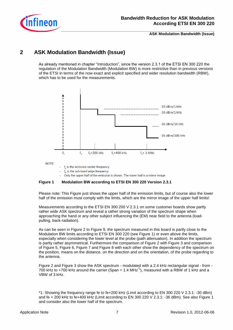
2 ASK Modulation Bandwidth (Issue)
As already mentioned in chapter “Introduction”, since the version 2.3.1 of the ETSI EN 300 220 the regulation of the Modulation Bandwidth (Modulation BW) is more restrictive than in previous versions of the ETSI in terms of the now exact and explicit specified and wider resolution bandwidth (RBW), which has to be used for the measurements.
Figure 1 Modulation BW according to ETSI EN 300 220 Version 2.3.1
Please note: This Figure just shows the upper half of the emission limits, but of course also the lower half of the emission must comply with the limits, which are the mirror image of the upper half limits! Measurements according to the ETSI EN 300 200 V 2.3.1 on some customer boards show partly rather wide ASK spectrum and reveal a rather strong variation of the spectrum shape when approaching the hand or any other subject influencing the (EM) near field to the antenna (load-pulling, back-radiation). As can be seen in Figure 2 to Figure 9, the spectrum measured in this board is partly close to the Modulation BW limits according to ETSI EN 300 220 (see Figure 1) or even above the limits, especially when considering the lower level at the probe (path attenuation). In addition the spectrum is partly rather asymmetrical. Furthermore the comparison of Figure 2 with Figure 3 and comparison of Figure 5, Figure 6, Figure 7 and Figure 8 with each other show the dependency of the spectrum on the position, means on the distance, on the direction and on the orientation, of the probe regarding to the antenna. Figure 2 and Figure 3 show the ASK spectrum - modulated with a 2.4 kHz rectangular signal - from -700 kHz to +700 kHz around the carrier (Span = 1.4 MHz
*1), measured with a RBW of 1 kHz and a
VBW of 3 kHz.
*1: Showing the frequency range fe to fe+200 kHz (Limit according to EN 300 220 V 2.3.1: -30 dBm) and fe + 200 kHz to fe+400 kHz (Limit according to EN 300 220 V 2.3.1: -36 dBm). See also Figure 1 and consider also the lower half of the spectrum.

Bandwidth Reduction for ASK Modulation According ETSI EN 300 220
ASK Modulation Bandwidth (Issue)
Application Note 8 Revision 1.0, 2012-06-06
Figure 2 Measurement 1 Span = 1 kHz & RBW = 1kHz
Figure 3 Measurement 2 Span = 1 kHz & RBW = 1 kHz
Figure 4 and Figure 5 show the ASK spectrum - modulated with a 2.4 kHz rectangular signal - from -1250 kHz to +1250 kHz around the carrier (Span = 2.5 MHz
*2), measured with a RBW of 10 kHz and
a VBW of 30 kHz.
Figure 4 Measurement 3 Span = 2.5 MHz & RBW = 10 kHz
Figure 5 Measurement 4 Span = 2.5 MHz & RBW = 10 kHz
*2: Including the frequency range fe+400 kHz to fe+1 MHz (Limit according to EN 300 220 V 2.3.1: -36 dBm @ RBW = 10 kHz). See also Figure 1 and consider also the lower half of the spectrum.
Bandwidth Reduction for ASK Modulation According ETSI EN 300 220
ASK Modulation Bandwidth (Issue)
Application Note 9 Revision 1.0, 2012-06-06
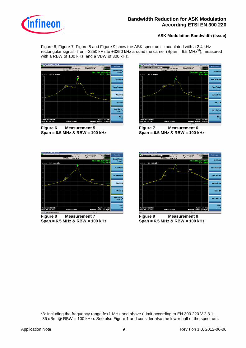
Figure 6, Figure 7, Figure 8 and Figure 9 show the ASK spectrum - modulated with a 2.4 kHz rectangular signal - from -3250 kHz to +3250 kHz around the carrier (Span = 6.5 MHz
*3), measured
with a RBW of 100 kHz and a VBW of 300 kHz.
Figure 6 Measurement 5 Span = 6.5 MHz & RBW = 100 kHz
Figure 7 Measurement 6 Span = 6.5 MHz & RBW = 100 kHz
Figure 8 Measurement 7 Span = 6.5 MHz & RBW = 100 kHz
Figure 9 Measurement 8 Span = 6.5 MHz & RBW = 100 kHz
*3: Including the frequency range fe+1 MHz and above (Limit according to EN 300 220 V 2.3.1: -36 dBm @ RBW = 100 kHz). See also Figure 1 and consider also the lower half of the spectrum.

Bandwidth Reduction for ASK Modulation According ETSI EN 300 220
Findings and Counter Measures
Application Note 10 Revision 1.0, 2012-06-06
3 Findings and Counter Measures
Analysis shows that the high steepness of the rising and/or falling edge and the asymmetry
*4 of the
data signal relating to the threshold levels of “ASK-modulator” (see Figure 11) enables or “amplifies” the effect of the back-radiation and load pulling, caused by the layout. Figure 10 shows the ASKDTA input circuit, which explains the typical threshold level of 1.1V.
+1.2 V
90 kW
6
50 pF 30 mA
60 kW
+1.1 V
VS
Figure 10 ASKDTA-pin Input Circuit
Figure 11 Lowpass Filter: Filtered & Un-Filtered Signal vs. Threshold
*4: The data signal is not centered around the logic low and logic high level (threshold) of the ASKDTA-input, consequently the steepness of the rising edge and the steepness of the falling edge are usually significantly different around the threshold level and the steepness of one of these edges (rather the rising edge) are rather high even when using a low-pass filter.
Bandwidth Reduction for ASK Modulation According ETSI EN 300 220
Findings and Counter Measures
Application Note 11 Revision 1.0, 2012-06-06
Figure 11 shows a 3V (low level is 0V, high level is 3V) ASK data signal once un-filtered (blue curve) and once filtered by a lowpass filter (red curve) compared to the typical threshold level (green doted line) and compared to the guaranteed minimum low level
*5 (brown doted line) and maximum high
level*5
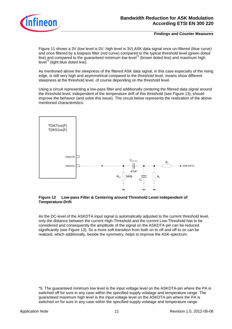
(light blue doted line). As mentioned above the steepness of the filtered ASK data signal, in this case especially of the rising edge, is still very high and asymmetrical compared to the threshold level, means show different steepness at the threshold level, of course depending on the threshold level. Using a circuit representing a low-pass filter and additionally centering the filtered data signal around the threshold level, independent of the temperature drift of this threshold (see Figure 13), should improve the behavior (and solve this issue). The circuit below represents the realization of the above mentioned characteristics:
TDA71xx(F)
TDK51xx(F)
ASKDTA
FSKDTA
ASK-DATA
CAC-OUT
RDC
R1
R2
C1
560k
47nF
Figure 12 Low-pass Filter & Centering around Threshold Level independent of Temperature-Drift
As the DC-level of the ASKDTA input signal is automatically adjusted to the current threshold level, only the distance between the current High-Threshold and the current Low-Threshold has to be considered and consequently the amplitude of the signal on the ASKDTA-pin can be reduced significantly (see Figure 13). So a more soft transition from both on to off and off to on can be realized, which additionally, beside the symmetry, helps to improve the ASK-spectrum.
*5: The guaranteed minimum low level is the input voltage level on the ASKDTA-pin where the PA is switched off for sure in any case within the specified supply volatage and temperature range. The guaranteed maximum high level is the input voltage level on the ASKDTA-pin where the PA is switched on for sure in any case within the specified supply volatage and temperature range

Bandwidth Reduction for ASK Modulation According ETSI EN 300 220
Findings and Counter Measures
Application Note 12 Revision 1.0, 2012-06-06
Figure 13 Signal-Shaping: Filtered & Un-Filtered Signal vs. Threshold
Please note that this circuit consists of only one more capacitor and two more resistors than a simple ordinary low-pass filter.
3.1 Data Signal: 1.4 V peak-peak / 2.4 kHz
Figure 11 shows the (calculated) transfer function of the circuit realized with the component values indicated below. These values given below are more or less adjusted for a 1.4 V peak-peak rectangular signal with a (fundamental) frequency of 2.4 kHz: R1 = 47k R2 = not used RDC = 560k C1 = 470pF CAC-OUT = 47nF
. Figure 14 Signal Shaping Circuit 1 Transfer Function

Bandwidth Reduction for ASK Modulation According ETSI EN 300 220
Findings and Counter Measures
Application Note 13 Revision 1.0, 2012-06-06
As can be seen at Figure 11, the transfer function of this circuit represents a band-pass characteristic, but with a lower cut-off frequency by far below the assumed (fundamental) frequency of the data signal of 2.4 kHz. The upper cut-off frequency is 10.08 kHz, which is 4.2 times higher than the assumed fundamental of the data signal and consequently yields still sufficiently steep edges for most applications. For some applications even a lower cut-off frequency or a lower ratio between the cut-off frequency and the data rate will be sufficient. The calculation is also considering the input impedance on the ASKDTA-pin.
3.2 Data Signal: 3 V peak-peak / 2.4 kHz
The given values given at 3.1 are more or less optimized for an applied (2.4 kHz) rectangular signal showing a peak-peak amplitude of 1.4V. For a 2.4 kHz rectangular signal with a peak-peak amplitude of e.g. ~3V the following values are recommended:
R1 = 100k R2 = 91k (approaching 88k) RDC = 560k C1 = 470pF CAC-OUT = 47nF
Figure 15 Signal Shaping Circuit 2 Transfer Function
Bandwidth Reduction for ASK Modulation According ETSI EN 300 220
Findings and Counter Measures
Application Note 14 Revision 1.0, 2012-06-06
3.3 Alternative circuit
Caution: The circuit shown in Figure 10 works pretty well for balanced codes
*6 like Manchester for
instance. In case of a very long low or high period the capacitor CAC-OUT has to be increased. Furthermore the values given at 3.1 and 3.2 are more or less optimized for a 2.4 kHz rectangular signal showing an amplitude of ~1.4 V peak-peak and ~3V peak-peak respectively, but if a battery is used and the data signal depends on the battery voltage, the lowest battery voltage has to be considered. On the other hand a more or less slight extension of the ASK bandwidth at the maximum supply voltage can be caused when adjusting the circuit to the lowest supply (battery) voltage, depending on the difference between the maximum and minimum supply voltage. An alternative (modified) circuit could be used if an asymmetrical data signal (NRZ) is used or if the “start-up” procedure and behavior e.g. preamble, …, causes an issue. This alternative circuit also regulates the signal level on the ASKDTA-pin - to the proper value - independent of the input signal level and consequently independent on the battery voltage of a battery driven application. So this alternative circuit can be used in case of an asymmetrical data signal and for regulating the signal on the ASKDTA-pin always to the optimum value, independent of the battery voltage. *6: The low and high time are equal over a certain (minimum) period of time.
Bandwidth Reduction for ASK Modulation According ETSI EN 300 220
Measurement Results
Application Note 15 Revision 1.0, 2012-06-06
4 Measurement Results
4.1 Frequency range fe to fe + 200 kHz & fe + 200 kHz to fe + 400 kHz
The measurements shown on the next pages (Figure 13 to Figure 24) in fact clearly proves that this simple signal shaping circuit significantly decreases the ASK-BW and makes it much less sensitive when the hand approaches the antenna, almost independent of the layout and matching.
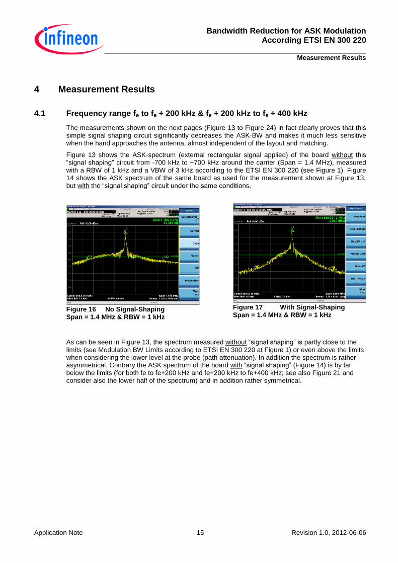
Figure 13 shows the ASK-spectrum (external rectangular signal applied) of the board without this “signal shaping” circuit from -700 kHz to +700 kHz around the carrier (Span = 1.4 MHz), measured with a RBW of 1 kHz and a VBW of 3 kHz according to the ETSI EN 300 220 (see Figure 1). Figure 14 shows the ASK spectrum of the same board as used for the measurement shown at Figure 13, but with the “signal shaping” circuit under the same conditions.
Figure 16 No Signal-Shaping Span = 1.4 MHz & RBW = 1 kHz
Figure 17 With Signal-Shaping Span = 1.4 MHz & RBW = 1 kHz
As can be seen in Figure 13, the spectrum measured without “signal shaping” is partly close to the limits (see Modulation BW Limits according to ETSI EN 300 220 at Figure 1) or even above the limits when considering the lower level at the probe (path attenuation). In addition the spectrum is rather asymmetrical. Contrary the ASK spectrum of the board with “signal shaping” (Figure 14) is by far below the limits (for both fe to fe+200 kHz and fe+200 kHz to fe+400 kHz; see also Figure 21 and consider also the lower half of the spectrum) and in addition rather symmetrical.
Bandwidth Reduction for ASK Modulation According ETSI EN 300 220
Measurement Results
Application Note 16 Revision 1.0, 2012-06-06
4.2 Frequency range fe + 400 kHz to fe + 1 MHz
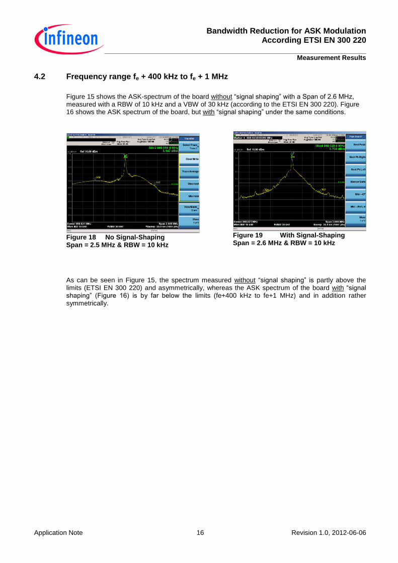
Figure 15 shows the ASK-spectrum of the board without “signal shaping” with a Span of 2.6 MHz, measured with a RBW of 10 kHz and a VBW of 30 kHz (according to the ETSI EN 300 220). Figure 16 shows the ASK spectrum of the board, but with “signal shaping” under the same conditions.
Figure 18 No Signal-Shaping Span = 2.5 MHz & RBW = 10 kHz
Figure 19 With Signal-Shaping Span = 2.6 MHz & RBW = 10 kHz
As can be seen in Figure 15, the spectrum measured without “signal shaping” is partly above the limits (ETSI EN 300 220) and asymmetrically, whereas the ASK spectrum of the board with “signal shaping” (Figure 16) is by far below the limits (fe+400 kHz to fe+1 MHz) and in addition rather symmetrically.
Bandwidth Reduction for ASK Modulation According ETSI EN 300 220
Measurement Results
Application Note 17 Revision 1.0, 2012-06-06
4.3 Frequency range fe + 1 MHz and above
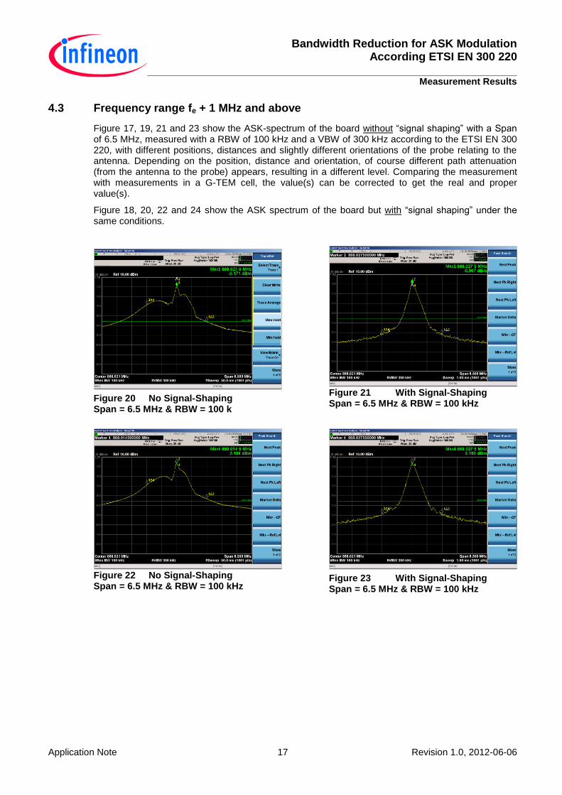
Figure 17, 19, 21 and 23 show the ASK-spectrum of the board without “signal shaping” with a Span of 6.5 MHz, measured with a RBW of 100 kHz and a VBW of 300 kHz according to the ETSI EN 300 220, with different positions, distances and slightly different orientations of the probe relating to the antenna. Depending on the position, distance and orientation, of course different path attenuation (from the antenna to the probe) appears, resulting in a different level. Comparing the measurement with measurements in a G-TEM cell, the value(s) can be corrected to get the real and proper value(s).
Figure 18, 20, 22 and 24 show the ASK spectrum of the board but with “signal shaping” under the same conditions.
Figure 20 No Signal-Shaping Span = 6.5 MHz & RBW = 100 k
Figure 21 With Signal-Shaping Span = 6.5 MHz & RBW = 100 kHz
Figure 22 No Signal-Shaping Span = 6.5 MHz & RBW = 100 kHz
Figure 23 With Signal-Shaping Span = 6.5 MHz & RBW = 100 kHz

Bandwidth Reduction for ASK Modulation According ETSI EN 300 220
Measurement Results
Application Note 18 Revision 1.0, 2012-06-06
Figure 24 No Signal-Shaping Span = 6.5 MHz & RBW = 100 kHz
Figure 25 With Signal-Shaping Span = 6.5 MHz & RBW = 100 kHz
Figure 26 No Signal-Shaping Span = 6.5 MHz & RBW = 100 kHz
Figure 27 With Signal-Shaping Span = 6.5 MHz & RBW = 100 kHz
The measurements (Figure 17, 19, 21 and 23) clearly show that the spectrum measured without “signal shaping” is partly by far above the limits (ETSI EN 300 220) and asymmetrical, whereas the ASK spectrum of the board with “signal shaping” is by far below the limits (fe+400 kHz to fe+1 MHz) and in addition rather symmetrical. Furthermore Figure 17, 19, 21 and 23 show that the spectrum of the board without “signal shaping” changes significantly when changing the position of the probe relative to the antenna, whereas the board with “signal shaping” (Figure 18, 20, 22 and 24) is quite insensitive to the influence of the probe, although the probe was extreme close or even toughing the antenna at the measurement shown at Figure 24. PS: Note that instead of the real data signal an external rectangular signal was applied as ASK-data signal, which means even disadvantageous condition / wider spectrum.

Bandwidth Reduction for ASK Modulation According ETSI EN 300 220
Conclusion
Application Note 19 Revision 1.0, 2012-06-06
5 Conclusion
1. The “signal shaping” circuit significantly reduces the ASK BW and makes it much less sensitive
when the hand (or anything else) approaches the antenna. 2. The measurement results are achieved with a cut-off frequency of the signal shaping circuit
(10.08 kHz), which is even 4.2 times higher than the frequency of the modulation signal (2.4 kHz). For some applications even a lower ratio between the cut-off frequency and the data rate will be sufficient, which would yield even better results.
3. This improvement is (almost) independent of the layout and matching. 4. Consequently the matching can also be optimized for a low level of the harmonics, like the 2
nd
and 3rd
harmonic. 5. The circuit only consists of 2 capacitors and 2 - 3 resistors, means only one more capacitor and
1 - 2 more resistor(s) than an “ordinary” low-pass filter circuit.

w w w . i n f i n e o n . c o m
Published by Infineon Technologies AG