Embed Size (px)
Citation preview

Band offsets and heterostructures of two-dimensional semiconductors
Jun Kang,1 Sefaattin Tongay,2 Jian Zhou,2 Jingbo Li,1,a) and Junqiao Wu2,3,a)
1Institute of Semiconductors, Chinese Academy of Sciences, PO Box 912, Beijing 100083,People’s Republic of China2Department of Materials Science and Engineering, University of California, Berkeley, California 94720, USA3Materials Sciences Division, Lawrence Berkeley National Laboratory, Berkeley, California 94720, USA
(Received 7 November 2012; accepted 18 December 2012; published online 9 January 2013)
The band offsets and heterostructures of monolayer and few-layer transition-metal dichalcogenides
MX2 (M¼Mo, W; X¼S, Se, Te) are investigated from first principles calculations. The band
alignments between different MX2 monolayers are calculated using the vacuum level as reference,
and a simple model is proposed to explain the observed chemical trends. Some of the monolayers
and their heterostructures show band alignments suitable for potential applications in spontaneous
water splitting, photovoltaics, and optoelectronics. The strong dependence of the band offset on the
number of layers also implicates a possible way of patterning quantum structures with thickness
engineering. VC 2013 American Institute of Physics. [http://dx.doi.org/10.1063/1.4774090]
After graphene became experimentally accessible in
2004,1 two-dimensional (2D) materials have attracted great
attention mainly due to their unique physical properties and
capability to fulfill the demands of future nanoelectronic
industry on flexibility, adaptability, and multi-functionality.2
Transition metal dichalcogenides MX2 (where M and X corre-
spond to transition metal and chalcogen, respectively) are
members of the layered materials like graphite. Soon after the
discovery of graphene, it was demonstrated that monolayer
MX2, such as MoS2 and NbSe2, could also be achieved using
mechanical exfoliation.3 More recently, various experimental
studies have reported the synthesis of MX2 monolayers, such
as MoS2, WS2, MoSe2, MoTe2, TiS2, TaS2, TaSe2, NiTe2, and
ZrS2.4–6 Bulk MoX2 and WX2 are indirect band-gap semicon-
ductors, whereas their monolayers have direct bandgaps,7–9
which are favorable for optoelectronic applications. The exis-
tence of the native bandgap provides an excellent current on/
off ratio of 108 in single-layer MoS2 based field-effect transis-
tors,10 and the application of monolayer MoS2 in integrated
circuits and logic operations has already been realized.11
Recently, the band structure of single- and few-layer
MX2 has been studied using first principles ab-initio calcula-
tions, focusing mostly on their bandgap values, while their
band offsets are much less explored. Band offsets of semicon-
ductors are important and necessary parameters in material
and device design. More specifically, the band offset is critical
to many properties such as quantum confinement,12 dopabil-
ity,13 and chemical activity.14 Moreover, designing hetero-
structure devices based on 2D semiconductors requires
accurate band offset parameters across different materials.
Heterojunctions interfacing different 2D materials would ena-
ble the so-called van der Waals epitaxy,15 in which the lattice
matching condition in traditional epitaxy is drastically relaxed,
allowing the formation of a wide range of 2D/2D, 2D/3D, or
even more advanced 3D/2D/3D heterostructures. Finally,
chemical trends of the band offsets provide a useful tool for
predicting physical properties of materials and heterostructure
geometries. Previously, the band offset between several bulk
MX2 has been investigated by Jiang.16 However, due to the
quantum confinement effect, the physical properties of the 2D
semiconductors are very different compared to their 3D coun-
terparts, and therefore the band offsets of single layer MX2 are
expected to show stark differences from the 3D case. So far,
band offsets of monolayer MX2 are completely unknown. In
this work, we study the electronic properties of MX2 mono-
layers and few layers (M¼Mo, W, and X¼S, Se, Te) using
first principles calculations, but focus on their band offsets and
interesting heterostructure geometries enabled by the band off-
sets. On the basis of the observed chemical trends, we discuss
implications for potential device applications.
The calculations were performed using the Vienna ab ini-tio simulation package (VASP).17 The six outmost electrons for
transition-metal and chalcogen were treated as valence elec-
trons. The core-valence interaction was described by the
frozen-core projector augmented wave (PAW) method.18 The
generalized gradient approximation of Perdew-Burke-Ernzer-
hof (GGA-PBE)19 was adopted for exchange-correlation
functional. Part of the calculations were also performed using
the Heyd-Scuseria-Ernzerhof (HSE06) hybrid functional.20
Energy cut off for plane-wave expansion was set to 400 eV.
Brillouin zone sampling was performed with Monkhorst-Pack
(MP) special k point meshes.21 For the hexagonal unit cell, a
grid of 24� 24� 1 was used (24� 24� 5 in bulk calcula-
tions), and the k-point grid scaled with respect to the supercell
size. A vacuum layer larger than 10 A was added to avoid
interaction between adjacent images. All atoms were allowed
to relax until the calculated Hellmann-Feynman force on each
atom was smaller than 0.01 eV/A. Spin-orbit interaction (SOI)
is included when calculating band structures. The vacuum
level was taken as zero reference in the calculations of band
alignment.
The monolayers of MX2 considered in this work have
hexagonal lattices with honeycomb structures (1 H-MX2)
similar to graphene. Basic lattice parameters and physical
properties of single-layer MX2 are listed in Table I, and the
calculated bandgap values are consistent with previous stud-
ies.9,22 Figure 1 shows the calculated band structure of
a)Authors to whom correspondence should be addressed. Electronic
addresses: [email protected] and [email protected].
0003-6951/2013/102(1)/012111/4/$30.00 VC 2013 American Institute of Physics102, 012111-1
APPLIED PHYSICS LETTERS 102, 012111 (2013)

MoS2, MoSe2, and WS2. While the lattice constants of
monolayer MX2 calculated by HSE06 are in excellent agree-
ment with known bulk values, those obtained by PBE are
slightly overestimated. Despite this slight discrepancy, we
note that these two methods provide similar physical trends;
i.e., when X goes from S to Te, the lattice constant and bond
length of MX2 increase associated with the increase in ionic
radius of X. We also note that the lattice constants of MoX2
and WX2 are very close to each other, indicating that synthe-
sizing MoX2-WX2 heterostructures might allow one to engi-
neer optical and physical properties with minimum structural
defects. Finally, elastic parameters which are obtained by fit-
ting the strain-energy relationship of MX2 monolayers show
that the in-plane stiffness decreases when X changes from S
to Te, and M changes from W to Mo. The calculated Pois-
son’s ratios of MX2 monolayer are around 0.2, and the Pois-
son’s ratio of MoX2 is found to be slightly larger than that of
WX2.
Previous studies have shown that MX2 monolayers pos-
sess direct bandgaps, with the conduction band maximum
(CBM) and valence band minimum (VBM) located at the K
symmetry points,7,9 as well as a significant spin-orbit split-
ting in valence band,5,23 consistent with our results as listed
in Table I. Comparing to the experimental values, we
observe that the bandgap values are underestimated by PBE
while they are slightly overestimated by HSE06. Here, we
note that regardless of the choice of the method (PBE/
HSE06), the observed general trends display similar behav-
ior. Therefore, the deviation from the experimentally
reported bandgap values can be omitted when comparing the
band offsets between MX2 monolayers, and hence the chem-
ical trends of band structures of MX2 can be properly
described by both PBE and HSE06.
The band alignment for MX2 monolayers is shown in
Fig. 2(a). In the following, we discuss the results in Fig. 2
based on PBE calculations, but similar results can be
deduced from the HSE06. Overall, the band offsets show the
following trends:
1. As the atomic number of X increases (from S to Te), the
energies of CBM and VBM of MX2 also increase. More-
over, the conduction band offset (CBO) is smaller than
the valence band offset (VBO). More specifically, the
VBM of MoSe2 is 0.63 eV higher than that of MoS2
while its CBM is 0.37 eV higher than that of MoS2.
Here, the only exception is WTe2 where its CBM is
slightly lower (by 0.06 eV) than that of WSe2.
2. For common-X system, the CBM and VBM of WX2 are
higher than those of MoX2, i.e., MoX2-WX2 lateral het-
erostructures have a type-II band alignment. For exam-
ple, the VBM of WS2 is 0.39 eV higher than that of
MoS2, and its CBM is 0.35 eV higher.
To understand the observed trends in the band offsets,
we look at the physical origin of the observed CBM and
VBM values. For simplifying, the following discussions are
made based on the band structure calculated without SOI.
(SOI only affects the CBM and VBM energies, while the
general trends of the band offsets were found to be the
same.) Taking MoS2 as an example, the VBM of MoS2
mainly consists of the dx2�y2 and dxy orbitals of Mo and the
px and py orbitals of S. In addition, it is found that the 5th
band at the K points, which locates about 4 eV lower than
the VBM, has the same character as VBM. Therefore, the
VBM of MoS2 originates mainly from the repulsion between
the dx2�y2 and dxy orbitals of Mo and the px and py orbitals of
S. The d orbital of Mo is higher than the p orbital of S, so it
is pushed up by D1, forming the VBM, and the p orbital is
pushed down by D10 , as shown in Fig. 2(b). The CBM of
MoS2 has the character of the dz2 orbital of Mo and the px
and py orbitals of S, while the 4th band at the K points,
located about 4.5 eV lower than the VBM, has the same char-
acter. Thus, the CBM of MoS2 originates from the repulsion
between the dz2 orbital of Mo and the px and py orbitals of S.
The dz2 orbital is pushed up by D2, forming the CBM, and
the p orbital is pusheddown by D20 . Using this model, we can
understand the trends of the band offsets of MX2.
For common-M systems, the VBO and CBO are deter-
mined by the repulsion strength D1 and D2 between the cat-
ion d orbitals and anion p orbitals. The magnitude of the
repulsion solely depends on the overlap integral of d and porbitals and their difference in energy. In principle, a larger
overlap integral or a smaller energy difference leads to larger
TABLE I. Calculated properties of MX2 monolayers: lattice constant a, M-X bond length d, bandgap Eg, spin-orbit splitting DSO in valence band, cohesive
energy EC per unit cell, charge transfer Dq of the M atom, Poisson’s ratio �, and in-plane stiffness C. a, d, Eg, and DSO calculated by HSE06 are also shown.
a (A) aHSE (A) d (A) dHSE (A) Eg (eV) EgHSE (eV) DSO (eV) DSO
HSE (eV) EC (eV) Dq (e) � C (N/m)
MoS2 3.18 3.16 2.41 2.40 1.59 2.02 0.15 0.20 15.31 1.09 0.25 124.24
MoSe2 3.32 3.29 2.54 2.51 1.33 1.72 0.19 0.27 13.70 0.85 0.23 103.40
MoTe2 3.55 3.52 2.73 2.70 0.94 1.28 0.22 0.35 12.01 0.52 0.24 78.90
WS2 3.18 3.16 2.42 2.40 1.55 1.98 0.43 0.56 17.28 1.24 0.22 139.54
WSe2 3.32 3.29 2.55 2.53 1.25 1.63 0.47 0.63 15.45 0.96 0.19 115.52
WTe2 3.55 3.52 2.74 2.71 0.75 1.03 0.49 0.69 13.51 0.57 0.18 86.93
FIG. 1. Band structure of monolayer MoS2, MoSe2, and WS2 calculated by
PBE.
012111-2 Kang et al. Appl. Phys. Lett. 102, 012111 (2013)
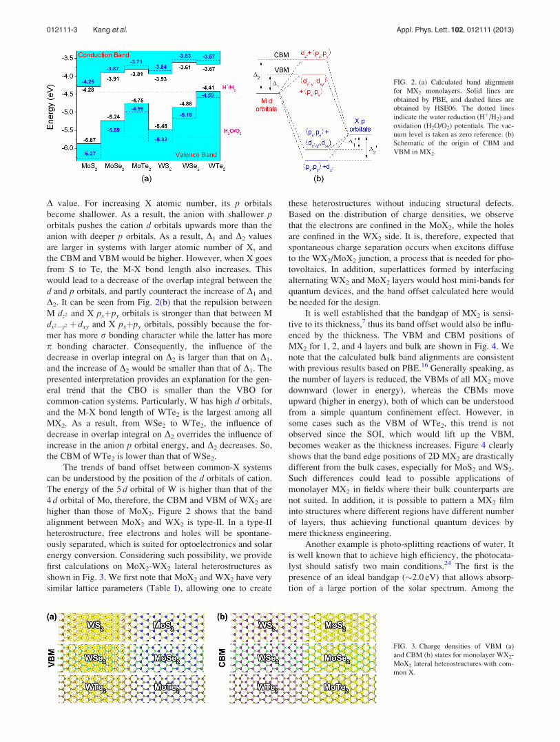
D value. For increasing X atomic number, its p orbitals
become shallower. As a result, the anion with shallower porbitals pushes the cation d orbitals upwards more than the
anion with deeper p orbitals. As a result, D1 and D2 values
are larger in systems with larger atomic number of X, and
the CBM and VBM would be higher. However, when X goes
from S to Te, the M-X bond length also increases. This
would lead to a decrease of the overlap integral between the
d and p orbitals, and partly counteract the increase of D1 and
D2. It can be seen from Fig. 2(b) that the repulsion between
M dz2 and X pxþpy orbitals is stronger than that between M
dx2�y2 þ dxy and X pxþpy orbitals, possibly because the for-
mer has more r bonding character while the latter has more
p bonding character. Consequently, the influence of the
decrease in overlap integral on D2 is larger than that on D1,
and the increase of D2 would be smaller than that of D1. The
presented interpretation provides an explanation for the gen-
eral trend that the CBO is smaller than the VBO for
common-cation systems. Particularly, W has high d orbitals,
and the M-X bond length of WTe2 is the largest among all
MX2. As a result, from WSe2 to WTe2, the influence of
decrease in overlap integral on D2 overrides the influence of
increase in the anion p orbital energy, and D2 decreases. So,
the CBM of WTe2 is lower than that of WSe2.
The trends of band offset between common-X systems
can be understood by the position of the d orbitals of cation.
The energy of the 5 d orbital of W is higher than that of the
4 d orbital of Mo, therefore, the CBM and VBM of WX2 are
higher than those of MoX2. Figure 2 shows that the band
alignment between MoX2 and WX2 is type-II. In a type-II
heterostructure, free electrons and holes will be spontane-
ously separated, which is suited for optoelectronics and solar
energy conversion. Considering such possibility, we provide
first calculations on MoX2-WX2 lateral heterostructures as
shown in Fig. 3. We first note that MoX2 and WX2 have very
similar lattice parameters (Table I), allowing one to create
these heterostructures without inducing structural defects.
Based on the distribution of charge densities, we observe
that the electrons are confined in the MoX2, while the holes
are confined in the WX2 side. It is, therefore, expected that
spontaneous charge separation occurs when excitons diffuse
to the WX2/MoX2 junction, a process that is needed for pho-
tovoltaics. In addition, superlattices formed by interfacing
alternating WX2 and MoX2 layers would host mini-bands for
quantum devices, and the band offset calculated here would
be needed for the design.
It is well established that the bandgap of MX2 is sensi-
tive to its thickness,7 thus its band offset would also be influ-
enced by the thickness. The VBM and CBM positions of
MX2 for 1, 2, and 4 layers and bulk are shown in Fig. 4. We
note that the calculated bulk band alignments are consistent
with previous results based on PBE.16 Generally speaking, as
the number of layers is reduced, the VBMs of all MX2 move
downward (lower in energy), whereas the CBMs move
upward (higher in energy), both of which can be understood
from a simple quantum confinement effect. However, in
some cases such as the VBM of WTe2, this trend is not
observed since the SOI, which would lift up the VBM,
becomes weaker as the thickness increases. Figure 4 clearly
shows that the band edge positions of 2D MX2 are drastically
different from the bulk cases, especially for MoS2 and WS2.
Such differences could lead to possible applications of
monolayer MX2 in fields where their bulk counterparts are
not suited. In addition, it is possible to pattern a MX2 film
into structures where different regions have different number
of layers, thus achieving functional quantum devices by
mere thickness engineering.
Another example is photo-splitting reactions of water. It
is well known that to achieve high efficiency, the photocata-
lyst should satisfy two main conditions.24 The first is the
presence of an ideal bandgap (�2.0 eV) that allows absorp-
tion of a large portion of the solar spectrum. Among the
FIG. 2. (a) Calculated band alignment
for MX2 monolayers. Solid lines are
obtained by PBE, and dashed lines are
obtained by HSE06. The dotted lines
indicate the water reduction (Hþ/H2) and
oxidation (H2O/O2) potentials. The vac-
uum level is taken as zero reference. (b)
Schematic of the origin of CBM and
VBM in MX2.
FIG. 3. Charge densities of VBM (a)
and CBM (b) states for monolayer WX2-
MoX2 lateral heterostructures with com-
mon X.
012111-3 Kang et al. Appl. Phys. Lett. 102, 012111 (2013)

MX2 monolayers studied here, MoS2 and WS2 meet this con-
dition. The second requirement is that the photocatalyst must
have suitable band edges to straddle the redox potentials of
water. The standard water redox potentials with respect to
the vacuum level are �4.44 eV for the reduction (Hþ/H2),
and �5.67 eV for the oxidation (H2O/O2).25 Jiang has shown
that bulk MX2 cannot be applied directly to overall photo-
splitting of water because their CBM or VBM positions are
not suitable.16 Our calculations show that indeed the CBMs
(VBMs) of bulk MoX2 and WX2 are higher than the reduc-
tion (oxidation) potential (Fig. 4), so they can only be used
for water reduction. However, according to Figs. 4(a), mono-
layer MoS2 satisfies this band edge requirement. The energy
of VBM of MoS2 monolayer is calculated to be �5.87 eV by
PBE and �6.27 eV by HSE06. Since PBE underestimates
the bandgap while HSE06 overestimates, it is reasonable to
expect that the actual VBM position of MoS2 monolayer lies
between �5.87 eV and �6.27 eV, which is lower than the
water oxidation potential. The CBMs of MoS2 calculated by
PBE and HSE06 are both around �4.3 eV, higher than the
water reduction potential. Therefore, MoS2 monolayer is a
good candidate for spontaneous photo-splitting of water. It
should be noted that the idea of using nano MoS2 for H2 evo-
lution is also proposed in several previous studies.26 In these
works, the activity of MoS2 is mostly related to edge states
or vacancies, hence the defect levels play important roles.
Our calculations show that MoS2 is suited for photo-splitting
of water even in the absence of defects.
In summary, we have provided band offset calculations
for various 2D semiconductors and investigated their elastic
and electronic properties from first principles calculations.
The calculated band offsets between MX2 reveal that as the
atomic number of M or X increases, the CBM and VBM
energy also increases, and the VBO is larger than the CBO for
common-cation pairs. We further show that the CBM and
VBM of MX2 originate from the repulsion between the cation
d and anion p orbitals, and the chemical trends of the band
offsets can be interpreted accordingly. The MoX2-WX2 lateral
heterostructures have type-II band alignment, and are suited
for optoelectronics and energy conversion, and MoS2 mono-
layer is a good candidate for spontaneous photo-splitting of
water.
J. Li gratefully acknowledges financial support from the
Natural Science Foundation for Distinguished Young
Scholar (Grant No. 60925016). This work was supported by
the National Basic Research Program of China (Grant No.
2011CB921901) and the External Cooperation Program of
Chinese Academy of Sciences. We acknowledge the com-
puting resources provided by the Supercomputing Center,
CNIC, CAS.
1K. S. Novoselov, A. K. Geim, S. V. Morozov, D. Jiang, Y. Zhang, S. V.
Dubonos, I. V. Grigorieva, and A. A. Firsov, Science 306, 666 (2004).2C. Castro Neto and K. S. Novoselov, Mater. Express 1, 10 (2011).3K. S. Novoselov, D. Jiang, F. Schedin, T. J. Booth, V. V. Khotkevich, S.
V. Morozov, and A. K. Geim, Proc. Natl. Acad. Sci. U.S.A 102, 10451
(2005).4J. N. Coleman, M. Lotya, A. O’Neill, S. D. Bergin, P. J. King, U. Khan, K.
Young, A. Gaucher, S. De, R. J. Smith et al., Science 331, 568 (2011).5S. Tongay, J. Zhou, C. Ataca, K. Lo, T. S. Matthews, J. Li, J. C. Grossman,
and J. Wu, Nano Lett. 12, 5576 (2012).6Z. Zeng, Z. Yin, X. Huang, H. Li, Q. He, G. Lu, F. Boey, and H. Zhang,
Angew. Chem., Int. Ed. 50, 11093 (2011).7K. Mak, C. Lee, J. Hone, J. Shan, and T. F. Heinz, Phys. Rev. Lett. 105,
136805 (2010).8W. S. Yun, S. W. Han, S. C. Hong, I. G. Kim, and J. D. Lee, Phys. Rev. B
85, 033305 (2012).9Y. Ding, Y. Wang, J. Ni, L. Shi, S. Shi, and W. Tang, Physica B 406, 2254
(2011).10B. Radisavljevic, A. Radenovic, J. Brivio, V. Giacometti, and A. Kis, Nat.
Nanotechnol. 6, 147 (2011).11B. Radisavljevic, M. B. Whitwicj, and A. Kis, ACS Nano 5, 9934 (2011).12J. Li and L. Wang, Appl. Phys. Lett. 85, 2929 (2004).13S. B. Zhang, S. H. Wei, and A. Zunger, Phys. Rev. Lett. 84, 1232 (2000).14L. Kavan, M. Graetzel, S. E. Gilbert, C. Klemenz, and H. J. Scheel, J. Am.
Chem. Soc. 118, 6716 (1996).15A. Koma, J. Cryst. Growth 201–202, 236 (1999).16H. Jiang, J. Phys. Chem. C 116, 7664 (2012).17G. Kresse and J. Furthmuller, Phys. Rev. B 54, 11169 (1996).18P. E. Blochl, Phys. Rev. B 50, 17953 (1994).19J. P. Perdew, K. Burke, and M. Ernzerhof, Phys. Rev. Lett. 77, 3865
(1996).20J. Heyd, G. E. Scuseria, and M. Ernzerhof, J. Chem. Phys. 118, 8207
(2003).21H. J. Monkhorst and J. D. Pack, Phys. Rev. B 13, 5188 (1976).22C. Ataca, H. Sahin, and S. Ciraci, J. Chem. Phys. C 116, 8983 (2012).23Z. Y. Zhu, Y. C. Cheng, and U. Schwingenschlogl, Phys. Rev. B 84,
153402 (2011).24Y. Gai, J. Li, S. S. Li, J. B. Xia, and S. H. Wei, Phys. Rev. Lett. 102,
036402 (2009).25V. Chakrapani, J. C. Angus, A. B. Anderson, S. D. Wolter, B. R. Stoner,
and G. Sumanasekera, Science 318, 1424 (2007).26J. V. Lauritsen, J. Kibsgaard, S. Helveg, H. Tops�e, B. S. Clausen, E.
Lægsgaard, and F. Besenbacher, Nat. Nanotechnol. 2, 53 (2007); C. Ataca
and S. Ciraci, Phys. Rev. B 85, 195410 (2012); T. F. Jaramillo, K. P.
J�rgensen, J. Bonde, J. H. Nielsen, S. Horch, and I. Chorkendorff, Science
317, 100 (2007).
FIG. 4. Band edge positions of MX2 as a function of the number of layers
calculated by PBE. The vacuum level is taken as zero reference. The dashed
lines indicate the water redox potentials.
012111-4 Kang et al. Appl. Phys. Lett. 102, 012111 (2013)