Embed Size (px)
Citation preview
Page 1
Copyright © 2017 Avnet, Inc. AVNET, “Reach Further,” and the AV logo are registered trademarks of Avnet, Inc. All other brands are the property of their respective owners.
LIT# 5290-DG-AES-EG-SOM-V1
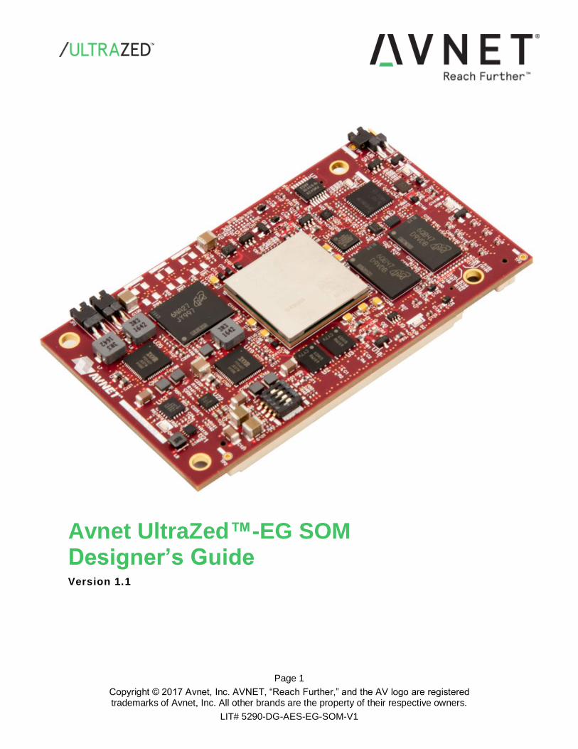
Avnet UltraZed™-EG SOM Designer’s Guide Version 1.1
Page 2
Document Control
Document Version: 1.1
Document Date: 1/25/2017
Prior Version History
Version Date Comment
1.1 1/25/2017
Page 3
Contents
1 Introduction .............................................................................................................. 5
2 UltraZed-EG SOM .................................................................................................... 6
3 UltraZed-EG SOM On-board Resources ................................................................ 8
3.1 Zynq UltraScale+ MPSoC XCZU3EG-1SFVA625 Device ........................................... 8
3.1.1 PS MIO Bank 500 .............................................................................................................. 8
3.1.2 PS MIO Bank 501 .............................................................................................................. 8
3.1.3 PS MIO Bank 502 .............................................................................................................. 9
3.1.4 PS Bank 503 ...................................................................................................................... 9
3.1.5 PS Bank 504 ...................................................................................................................... 9
3.1.6 PS Bank 505 ...................................................................................................................... 9
3.1.7 PL Bank 0 .......................................................................................................................... 9
3.1.8 PL Bank 26, 64, 65, and 66 ............................................................................................... 9
3.2 DDR4 SDRAM ............................................................................................................ 10
3.3 Dual Parallel QSPI Flash............................................................................................ 10
3.4 eMMC Flash ............................................................................................................... 10
3.5 USB 2.0 PHY .............................................................................................................. 11
3.6 Ethernet PHY .............................................................................................................. 12
3.7 PS Reference Clock Input .......................................................................................... 12
3.8 MPSoC Real-Time Clock (RTC) ................................................................................ 12
3.9 I2C EEPROM.............................................................................................................. 12
3.10 I2C 8-Bit I/O Expander ............................................................................................... 13
3.11 2-Channel I2C Switch/Mux ......................................................................................... 13
3.12 PS Boot Mode Switch ................................................................................................. 14
3.13 PMBus Interface ......................................................................................................... 15
3.14 SOM Reset Structure ................................................................................................. 16
3.15 PS Power-On Reset (POR) Circuit ............................................................................ 17
3.16 SOM Reset Input ........................................................................................................ 17
3.17 Carrier Card Reset Output ......................................................................................... 18
3.18 MPSoC Heat Sink with Fan ........................................................................................ 18
3.19 Voltage Regulators ..................................................................................................... 18
Page 4
4 UltraZed-EG SOM External Interfaces .................................................................. 19
4.1 PS MIO Interface ........................................................................................................ 21
4.2 PS USB 2.0 Connector Interface ............................................................................... 22
4.3 PS RJ45 Connector Interface .................................................................................... 23
4.4 PS GTR Transceiver Interface ................................................................................... 23
4.5 PL HD I/O Pins ........................................................................................................... 24
4.6 PL HP I/O Pins ........................................................................................................... 24
4.7 PL SYSMON Interface ............................................................................................... 24
4.8 SOM Reset Input ........................................................................................................ 25
4.9 Carrier Card Reset Output ......................................................................................... 25
4.10 Carrier Card I2C Interface .......................................................................................... 26
4.11 Ethernet MAC ID ........................................................................................................ 26
4.12 JTAG Interface ........................................................................................................... 27
4.13 PMBus Interface ......................................................................................................... 28
4.14 Power Requirements .................................................................................................. 29
4.15 Power Sequencing ..................................................................................................... 30
4.16 Power Estimation Using XPE ..................................................................................... 30
4.17 MPSoC Heat Sink with Fan ........................................................................................ 30
5 UltraZed-EG SOM JX Micro Connectors .............................................................. 31
5.1 Custom Carrier Cards Mating JX Receptacle Connectors ........................................ 31
6 UltraZed-EG SOM Mechanical Dimensions .......................................................... 39
7 Carrier Card PCB Design Guidelines .................................................................... 40
7.1 Connector Land and Alignment.................................................................................. 40
7.2 USB and Ethernet Connector Signal Routing ............................................................ 40
7.3 PS GTR Transceiver Signal Routing ......................................................................... 41
7.4 PS MIO Routing .......................................................................................................... 41
7.5 PL SYSMON Signal Routing ...................................................................................... 41
7.6 PL Single-Ended and Differential Signal Routing ...................................................... 42
7.7 JTAG Interface Signal Routing ................................................................................... 42
7.8 VIN Decoupling Caps ................................................................................................. 42
7.9 Mechanical Considerations ........................................................................................ 43
7.10 Thermal Considerations ............................................................................................. 44
8 Getting Help and Support ...................................................................................... 46
9 JX1, JX2, and JX3 Routed Net Lengths................................................................ 47
10 UltraZed-EG SOM Schematics.............................................................................. 52
11 Avnet UltraZed IO Carrier Card Schematics ......................................................... 53
Page 5
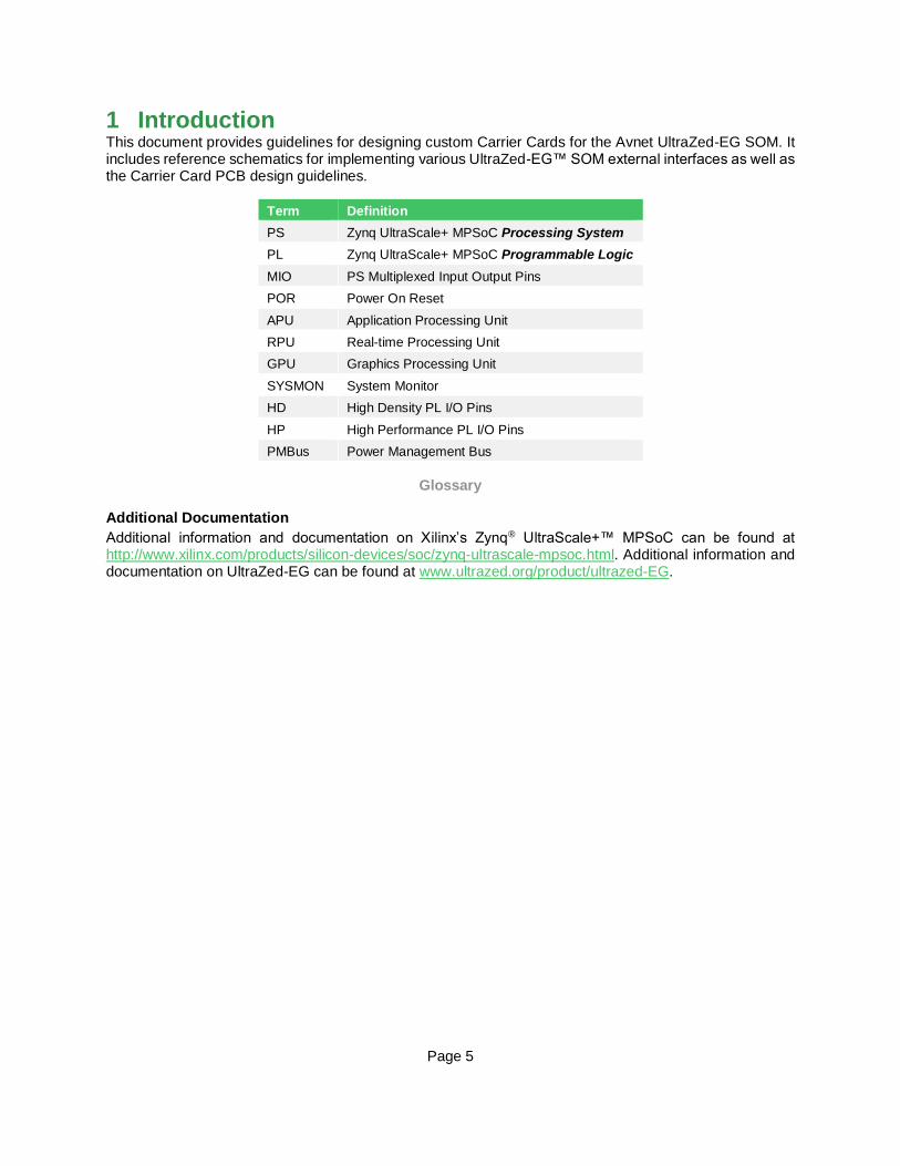
1 Introduction This document provides guidelines for designing custom Carrier Cards for the Avnet UltraZed-EG SOM. It includes reference schematics for implementing various UltraZed-EG™ SOM external interfaces as well as the Carrier Card PCB design guidelines.
Term Definition
PS Zynq UltraScale+ MPSoC Processing System
PL Zynq UltraScale+ MPSoC Programmable Logic
MIO PS Multiplexed Input Output Pins
POR Power On Reset
APU Application Processing Unit
RPU Real-time Processing Unit
GPU Graphics Processing Unit
SYSMON System Monitor
HD High Density PL I/O Pins
HP High Performance PL I/O Pins
PMBus Power Management Bus
Glossary
Additional Documentation
Additional information and documentation on Xilinx’s Zynq® UltraScale+™ MPSoC can be found at http://www.xilinx.com/products/silicon-devices/soc/zynq-ultrascale-mpsoc.html. Additional information and documentation on UltraZed-EG can be found at www.ultrazed.org/product/ultrazed-EG.
Page 6
2 UltraZed-EG SOM Avnet UltraZed-EG SOM is a highly integrated System-on-Module (SOM) designed based on the Xilinx powerful Zynq UltraScale+ MPSoC family of devices. Designed in a small form factor, the UltraZed-EG SOM packages all the necessary functions such as system memory, Ethernet, USB, and configuration memory needed for an embedded processing system. Although, initially released with the Xilinx XCZU3EG device, the UltraZed-EG SOM will be pin and form factor compatible with the XCZU2EG or XCZU3CG/XCZU2CG (UltraZed-CG) versions using the MPSoC device in the same package as the XCZU3EG device.
The UltraZed-EG SOM is offered in commercial and industrial temperatures and supports the following features:
– Xilinx XCZU3EG-1SFVA625 device
– DDR4 SDRAM (2GB, x32)
– Dual QSPI Flash (64MB)
– I2C EEPROM (2Kb)
– eMMC Flash (8GB, x8)
– USB 2.0 ULPI PHY
– Gigabit Ethernet PHY
– I2C 8-bit I/O expander
– 2-channel I2C switch/mux
– PS reference clock input
– On-board PMBus voltage regulators
– Power-On Reset (POR) circuit
– A 4-position boot mode DIP switch
– 3 JX micro-header connectors (2 x 140-pin, 1 x 100-pin) providing the following connections to the custom Carrier Cards (signal directions are with respect to the UltraZed-EG SOM):
– 180 user PL I/O pins
– 26 user PS MIO pins (one full MIO bank)
– 4 PS GTR transceivers
– 4 PS GTR reference clock inputs
– PS JTAG interface
– PL SYSMON interface
– USB 2.0 connector interface
– Gigabit Ethernet RJ45 connector interface
– PMBus interface
– SOM PS VBATT battery input
– Carrier Card I2C interface
– SOM Reset input
– Carrier Card interrupt input
– Carrier Card Reset output
– Power Good output
– SOM to Carrier Card ground pins
– SOM input voltages and output sense pins
Page 7
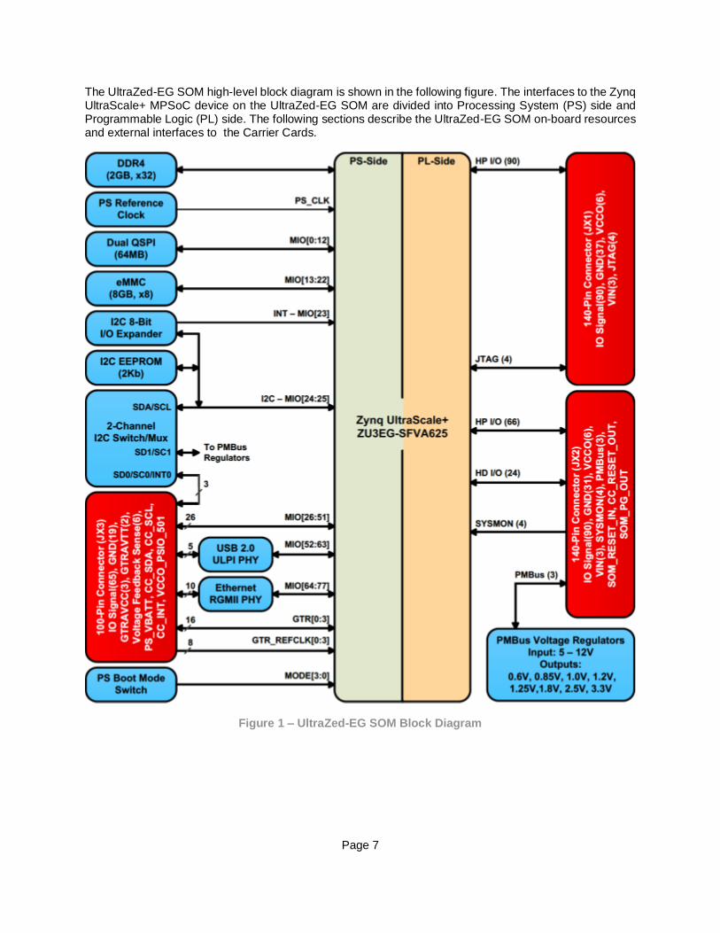
The UltraZed-EG SOM high-level block diagram is shown in the following figure. The interfaces to the Zynq UltraScale+ MPSoC device on the UltraZed-EG SOM are divided into Processing System (PS) side and Programmable Logic (PL) side. The following sections describe the UltraZed-EG SOM on-board resources and external interfaces to the Carrier Cards.
Figure 1 – UltraZed-EG SOM Block Diagram
Page 8
3 UltraZed-EG SOM On-board Resources The following sections provide a brief description of each component/resource available on the UltraZed-EG SOM.
Please refer to the Avnet UltraZed-EG SOM schematic at the end of this document for more information on the UltraZed-EG SOM on-board resources.
3.1 Zynq UltraScale+ MPSoC XCZU3EG-1SFVA625 Device The UltraZed-EG SOM utilizes the Xilinx XCZU3EG-SFVA625 device in -1 speed grade part (the UltraZed-EG SOM is designed to support all speed grades for the XCZU3EG-SFVA625 device). The XCZU3EG-1SFVA625 device supports APU speed of 1.2GHz (max), RPU speed of 500MHz (max), GPU speed of 600MHz (max), and DDR4 speed of up to 2133Mbps. The ZU3EG-A625 device features the following resources:
– 78 PS MIO pins (3 banks of MIOs, PS banks 500, 501, and 502, with 26 pins/bank)
– 4 PS GTR transceivers along with 4 PS GTR reference clock inputs (PS bank 505)
– PS DDR4 x32 interface (PS bank 504)
– PS JTAG interface (PS bank 503)
– Real-Time Clock (PS bank 503)
– PL SYSMON interface (PL bank 0)
– 24 PL HD (High Density) I/O pins (PL bank 26)
– 156 PL HP (High Performance) I/O pins (PL banks 64, 65, and 66)
The following sections provide brief descriptions of how each XCZU3EG MPSoC bank is used on the Avnet UltraZed-EG SOM followed by detail descriptions in subsequent sections.
3.1.1 PS MIO Bank 500 The PS MIO bank 500 consists of 26 MIO pins, MIO[0:25]. The MIO pins for this bank are operated at 1.8V and used to implement the following interfaces on the UltraZed-EG SOM:
– Dual Parallel (x8) QSPI Flash
– eMMC x8 Flash
– I2C EEPROM (2Kb)
– I2C 8-bit I/O expander
– I2C 2-channel switch/mux
– Carrier Card I2C interface
– I2C interface to the PMBus voltage regulators
3.1.2 PS MIO Bank 501 The PS bank 501 consists of 26 MIO pins, MIO[26:51]. These MIO pins are routed to the JX3 connector and are available to the custom Carrier Cards. The PS bank 501 I/O can be operated at 1.8V, 2.5V, or 3.3V set by the user via JX3 connector. This full bank of MIO pins can be used on a custom Carrier Card to implement various interfaces. On the Avnet UltraZed IO Carrier Card, PS MIO bank 501 are operated at 3.3V and used to implement the following interfaces:
– microSD card
– Dual USB-UART ports
– PS PMOD header
– PS user LED and push switch
– Display Port auxiliary interface
Page 9
3.1.3 PS MIO Bank 502 The PS bank 502 consists of 26 MIO pins, MIO[52:77]. The MIO pins for this bank are operated at 1.8V and used to implement the following interfaces on the UltraZed-EG SOM (please refer to the USB 2.0 PHY and Ethernet PHY sections of this document for more information):
– USB 2.0 ULPI PHY interface
– Gigabit Ethernet RGMII PHY interface
3.1.4 PS Bank 503 The PS bank 503 consists of JTAG, reset, PS reference clock input, boot mode, RTC crystal input, and few configuration pins. The reset, PS reference clock input, boot mode, RTC crystal input, and the configuration pins of the PS bank 503 pins are used on the UltraZed-EG SOM while the JTAG pins are routed to the JX1 connector. The PS bank 503 I/O is operated at 1.8V.
Zynq UltraScale+ MPSoC provides a built-in Real-Time Clock (RTC). A 32.768 KHz crystal is connected to the PS bank 503 PS_PADI and PS_PADO pins for the RTC. The on-chip RTC uses the PS_VBATT pin (provided by the Carrier Card via JX3 connector) for the backup battery. Carrier Cards drive the PS_VBATT pin with a 1.5V battery.
3.1.5 PS Bank 504 The PS bank 504 consists of DDR4 interface pins. These pins are used on the UltraZed-EG SOM to implement the DDR4 x32 memory interface. The PS bank 504 I/O is operated at 1.2V.
3.1.6 PS Bank 505 The PS bank 505 consists of PS GTR transceiver and their associated reference clock input pins (PS provides 4 GTR transceivers along with 4 reference clock inputs). These pins are routed to the JX3 connector and are available to the custom Carrier Cards. The GTR transceiver power rails (0.85V and 1.8V) are supplied by the custom Carrier Cards via JX3 connector.
3.1.7 PL Bank 0 The PL bank 0 consists of System Monitor (SYSMON) pins. These pins are routed to the JX2 connector and are available to the custom Carrier Cards. The System Monitor supply voltages (VCCADC and VREF) are provided on the UltraZed-EG SOM.
3.1.8 PL Bank 26, 64, 65, and 66 The PL HD bank 26 and HP banks 64, 65, and 66 provide 24 HD (High Density, bank 26) and 156 HP (High Performance, banks 64, 65, and 66) I/O pins. These pins are routed to the JX1/JX2 connectors and are available to the custom Carrier Cards. The PL HP banks I/O pins can be operated at 1.0V – 1.8V while the PL HD bank I/O pins can be operated at 1.2V – 3.3V. The VCCO voltages for the PL HD and HP banks are provided by the custom Carrier Cards via JX1/JX2 connectors.
Page 10
3.2 DDR4 SDRAM The UltraZed-EG SOM provides 2GB of DDR4 memory in x32 configuration using 2 Micron MT40A512M16JY-083E IT:B (96-pin BGA package) x16 devices. This device is implemented in 512Mb x 16 configuration and supports up to 2400Mbps data rate. The DDR4 devices are connected to the PS bank 504 and operated at 1.2V.
3.3 Dual Parallel QSPI Flash The UltraZed-EG SOM provides 64MB of QSPI Flash in dual-parallel (x8) configuration. Two Micron MT25QU256ABA1EW7-0SIT (8-pin W-PDFN package) devices are used to implement the parallel Flash interface on the UltraZed-EG SOM. The QSPI Flash devices are connected to the PS MIO bank 500 and operated at 1.8V I/O. The QSPI Flash can be used as a primary boot device on the UltraZed-EG SOM.
Signal Name MIO Pin # Notes
CLK_1 MIO[0] Lower QSPI device clock
DATA[1]_1 MIO[1] Lower QSPI device DATA[1]
DATA[2]_1 MIO[2] Lower QSPI device DATA[2]
DATA[3]_1 MIO[3] Lower QSPI device DATA[3]
DATA[0]_1 MIO[4] Lower QSPI device DATA[0]
CS_1 MIO[5] Lower QSPI device chip select
Feedback CLK MIO[6] No Connect
CS_2 MIO[7] Upper QSPI device chip select
DATA[0]_2 MIO[8] Upper QSPI device DATA[0]
DATA[1]_2 MIO[9] Upper QSPI device DATA[1]
DATA[2]_2 MIO[10] Upper QSPI device DATA[2]
DATA[2]_2 MIO[11] Upper QSPI device DATA[3]
CLK_2 MIO[12] Upper QSPI device clock
Table 1 – Dual-Parallel QSPI Flash Interface Pin Assignments
3.4 eMMC Flash The UltraZed-EG SOM provides 8GB of eMMC Flash to be used as a primary and/or secondary boot device. A single Micron MTFC8GAKAJCN-4M IT (153-pin VFBGA package) device is used to implement the eMMC Flash x8 interface. The eMMC device is connected to the PS MIO bank 500 and operated at 1.8V I/O. P0 port of the SOM I2C 8-bit I/O expander can be used to soft reset the eMMC device (please refer to the I2C 8-Bit I/O Expander section of this document for more information).
Signal Name MIO Pin # Notes
DATA[0] MIO[13] eMMC DATA[0]
DATA[1] MIO[14] eMMC DATA[1]
DATA[2] MIO[15] eMMC DATA[2]
DATA[3] MIO[16] eMMC DATA[3]
DATA[4] MIO[17] eMMC DATA[4]
DATA[5] MIO[18] eMMC DATA[5]
DATA[6] MIO[19] eMMC DATA[6]
DATA[7] MIO[20] eMMC DATA[7]
CMD MIO[21] eMMC Command
CLK MIO[22] eMMC Clock
Table 2 – eMMC Flash Interface Pin Assignments
Page 11
3.5 USB 2.0 PHY The UltraZed-EG SOM provides a single USB 2.0 PHY interface using the Microchip USB3320 USB 2.0 ULPI PHY in 32-pin QFN package. The USB 2.0 ULPI PHY connector side (connected to the JX3 connector) along with the PS USB 3.0 port (PS GTR[x]), connected to the JX3 connector) can be used on custom Carrier Cards to implement a USB 2.0/3.0 interface via a single connector. Please refer to the UltraZed-EG SOM External Interfaces section of this document for more information.
The USB 2.0 ULPI PHY host side I/O is connected to the PS MIO bank 502 and operated at 1.8V on the UltraZed-EG SOM. P1 port of the I2C 8-bit I/O expander can be used to soft reset the USB 2.0 ULPI PHY (please refer to the I2C 8-Bit I/O Expander section of this document for more information). Custom Carrier Cards have the option of not implementing the USB 3.0 portion of this interface.
Signal Name MIO Pin # Notes
CLK MIO[52] ULPI PHY clock input
DIR MIO[53] Controls the direction of the data bus
DATA[2] MIO[54] Host side DATA[2]
NXT MIO[55] This signal is used to throttle the data
DATA[0] MIO[56] Host side DATA[0]
DATA[1] MIO[57] Host side DATA[1]
STP MIO[58] Stops the data stream currently on the bus
DATA[3] MIO[59] Host side DATA[3]
DATA[4] MIO[60] Host side DATA[4]
DATA[5] MIO[61] Host side DATA[5]
DATA[6] MIO[62] Host side DATA[6]
DATA[7] MIO[63] Host side DATA[7]
Table 3 – USB 2.0 ULPI PHY Host Interface Side Pin Assignments
Page 12
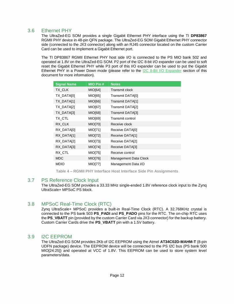
3.6 Ethernet PHY The UltraZed-EG SOM provides a single Gigabit Ethernet PHY interface using the TI DP83867 RGMII PHY device in 48-pin QFN package. The UltraZed-EG SOM Gigabit Ethernet PHY connector side (connected to the JX3 connector) along with an RJ45 connector located on the custom Carrier Card can be used to implement a Gigabit Ethernet port.
The TI DP83867 RGMII Ethernet PHY host side I/O is connected to the PS MIO bank 502 and operated at 1.8V on the UltraZed-EG SOM. P2 port of the I2C 8-bit I/O expander can be used to soft reset the Gigabit Ethernet PHY while P3 port of this I/O expander can be used to put the Gigabit Ethernet PHY in a Power Down mode (please refer to the I2C 8-Bit I/O Expander section of this document for more information).
Signal Name MIO Pin # Notes
TX_CLK MIO[64] Transmit clock
TX_DATA[0] MIO[65] Transmit DATA[0]
TX_DATA[1] MIO[66] Transmit DATA[1]
TX_DATA[2] MIO[67] Transmit DATA[2]
TX_DATA[3] MIO[68] Transmit DATA[3]
TX_CTL MIO[69] Transmit control
RX_CLK MIO[70] Receive clock
RX_DATA[0] MIO[71] Receive DATA[0]
RX_DATA[1] MIO[72] Receive DATA[1]
RX_DATA[2] MIO[73] Receive DATA[2]
RX_DATA[3] MIO[74] Receive DATA[3]
RX_CTL MIO[75] Receive control
MDC MIO[76] Management Data Clock
MDIO MIO[77] Management Data I/O
Table 4 – RGMII PHY Interface Host Interface Side Pin Assignments
3.7 PS Reference Clock Input The UltraZed-EG SOM provides a 33.33 MHz single-ended 1.8V reference clock input to the Zynq UltraScale+ MPSoC PS block.
3.8 MPSoC Real-Time Clock (RTC) Zynq UltraScale+ MPSoC provides a built-in Real-Time Clock (RTC). A 32.768KHz crystal is connected to the PS bank 503 PS_PADI and PS_PADO pins for the RTC. The on-chip RTC uses the PS_VBATT pin (provided by the custom Carrier Card via JX3 connector) for the backup battery. Custom Carrier Cards drive the PS_VBATT pin with a 1.5V battery.
3.9 I2C EEPROM The UltraZed-EG SOM provides 2Kb of I2C EEPROM using the Atmel AT34C02D-MAHM-T (8-pin UDFN package) device. The EEPROM device will be connected to the PS I2C bus (PS bank 500 MIO[24:25]) and operated at VCC of 1.8V. This EEPROM can be used to store system level parameters/data.
Page 13
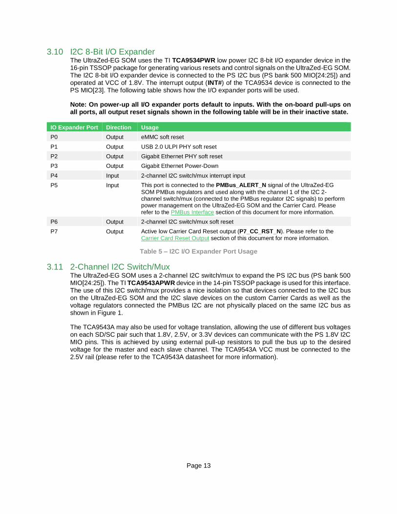
3.10 I2C 8-Bit I/O Expander The UltraZed-EG SOM uses the TI TCA9534PWR low power I2C 8-bit I/O expander device in the 16-pin TSSOP package for generating various resets and control signals on the UltraZed-EG SOM. The I2C 8-bit I/O expander device is connected to the PS I2C bus (PS bank 500 MIO[24:25]) and operated at VCC of 1.8V. The interrupt output (INT#) of the TCA9534 device is connected to the PS MIO[23]. The following table shows how the I/O expander ports will be used.
Note: On power-up all I/O expander ports default to inputs. With the on-board pull-ups on all ports, all output reset signals shown in the following table will be in their inactive state.
IO Expander Port Direction Usage
P0 Output eMMC soft reset
P1 Output USB 2.0 ULPI PHY soft reset
P2 Output Gigabit Ethernet PHY soft reset
P3 Output Gigabit Ethernet Power-Down
P4 Input 2-channel I2C switch/mux interrupt input
P5 Input This port is connected to the PMBus_ALERT_N signal of the UltraZed-EG
SOM PMBus regulators and used along with the channel 1 of the I2C 2-channel switch/mux (connected to the PMBus regulator I2C signals) to perform power management on the UltraZed-EG SOM and the Carrier Card. Please refer to the PMBus Interface section of this document for more information.
P6 Output 2-channel I2C switch/mux soft reset
P7 Output Active low Carrier Card Reset output (P7_CC_RST_N). Please refer to the Carrier Card Reset Output section of this document for more information.
Table 5 – I2C I/O Expander Port Usage
3.11 2-Channel I2C Switch/Mux The UltraZed-EG SOM uses a 2-channel I2C switch/mux to expand the PS I2C bus (PS bank 500 MIO[24:25]). The TI TCA9543APWR device in the 14-pin TSSOP package is used for this interface. The use of this I2C switch/mux provides a nice isolation so that devices connected to the I2C bus on the UltraZed-EG SOM and the I2C slave devices on the custom Carrier Cards as well as the voltage regulators connected the PMBus I2C are not physically placed on the same I2C bus as shown in Figure 1.
The TCA9543A may also be used for voltage translation, allowing the use of different bus voltages on each SD/SC pair such that 1.8V, 2.5V, or 3.3V devices can communicate with the PS 1.8V I2C MIO pins. This is achieved by using external pull-up resistors to pull the bus up to the desired voltage for the master and each slave channel. The TCA9543A VCC must be connected to the 2.5V rail (please refer to the TCA9543A datasheet for more information).
Page 14
P6 port of the I2C 8-bit I/O expander can be used to soft reset the 2-channel I2C switch/mux device. The following table shows how each TCA9543A channel will be used.
I2C Switch Channel Usage Notes
Master Channel
(SDA/SCL/INT)
This channel is connected to the PS I2C port, MIO[24:25] and
operated at 1.8V. The master INT output is connected to the P4 port of the I2C 8-bit I/O expander.
Pulled-up to 1.8V
On the SOM
Slave Channel 0
(SD0/SC0/INT0)
This channel is connected to the JX3 connector (CC_SDA, CC_SCL , and CC_INT_N signals) to allow slave I2C devices on the Carrier Card to be virtually placed on the same PS I2C bus (MIO[24:25]) as the I2C devices on the UltraZed-EG SOM so that software can use a single PS I2C core to communicate will all I2C devices in the system. Please refer to the Carrier Card I2C Interface section of this document for more information.
Pulled-up to 1.8V, 2.5V, or 3.3V On the Carrier Card
Slave Channel 1
(SD1/SC1/INT1)
This channel is connected to the PMBus (PMBus_DATA and
PMBus_CLK signals) of the UltraZed-EG SOM PMBus voltage regulators and used to control all PMBus voltage regulators on the UltraZed-EG SOM as well as the Carrier Card (the PMBus is connected to the Carrier Card via JX2 connector).
This feature allows the PS to control/monitor the PMBus voltage
regulators on the UltraZed-EG SOM as well as the Carrier Card for the purpose of power management and/or measurements. Please refer to the PMBus Interface section of this document for more information.
Pulled-up to 3.3V
On the SOM
The unused
slave channel 1 INT1 input must be pulled up to the VCC (2.5V) rail.
Table 6 – I2C Switch/Mux Channel Usage
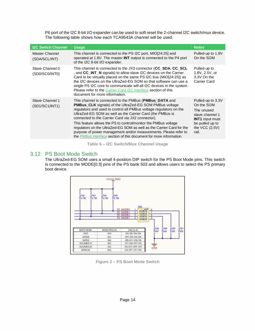
3.12 PS Boot Mode Switch The UltraZed-EG SOM uses a small 4-position DIP switch for the PS Boot Mode pins. This switch is connected to the MODE[0:3] pins of the PS bank 503 and allows users to select the PS primary boot device.
Figure 2 – PS Boot Mode Switch
Page 15
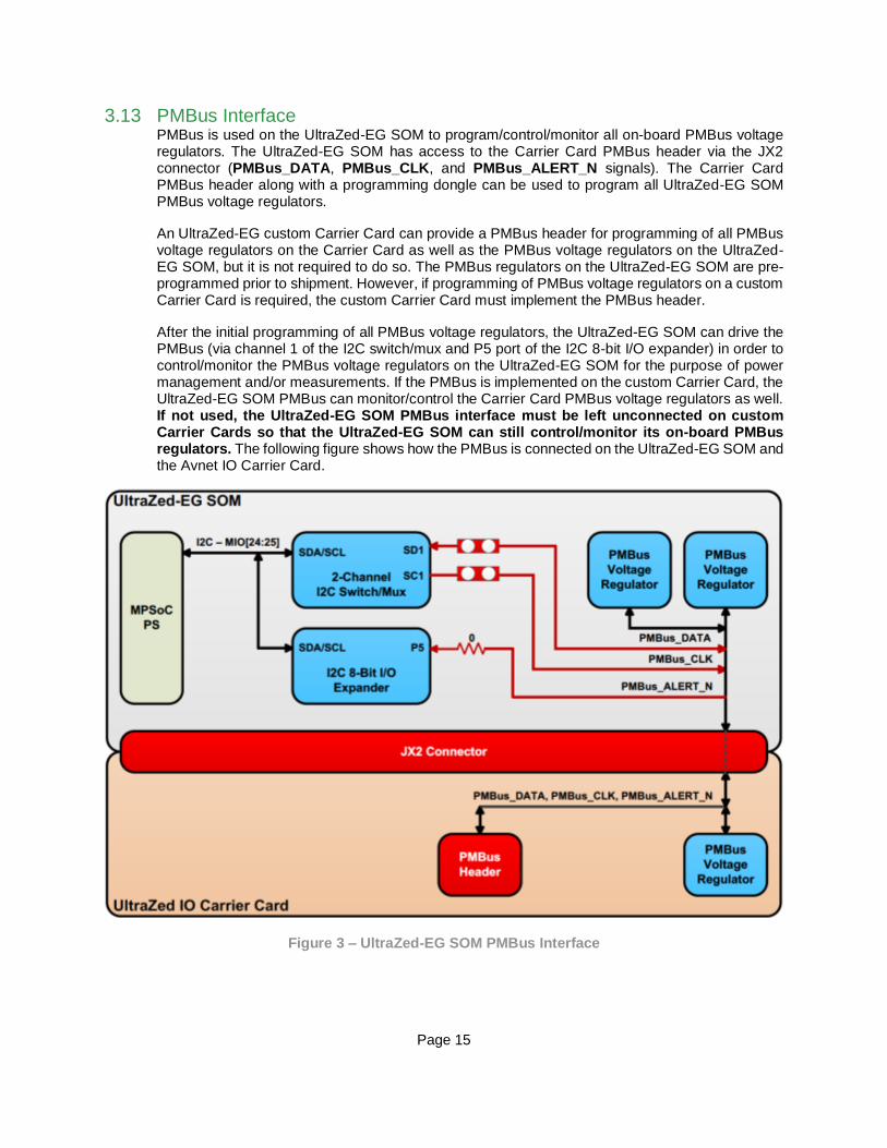
3.13 PMBus Interface PMBus is used on the UltraZed-EG SOM to program/control/monitor all on-board PMBus voltage regulators. The UltraZed-EG SOM has access to the Carrier Card PMBus header via the JX2 connector (PMBus_DATA, PMBus_CLK, and PMBus_ALERT_N signals). The Carrier Card PMBus header along with a programming dongle can be used to program all UltraZed-EG SOM PMBus voltage regulators.
An UltraZed-EG custom Carrier Card can provide a PMBus header for programming of all PMBus voltage regulators on the Carrier Card as well as the PMBus voltage regulators on the UltraZed-EG SOM, but it is not required to do so. The PMBus regulators on the UltraZed-EG SOM are pre-programmed prior to shipment. However, if programming of PMBus voltage regulators on a custom Carrier Card is required, the custom Carrier Card must implement the PMBus header.
After the initial programming of all PMBus voltage regulators, the UltraZed-EG SOM can drive the PMBus (via channel 1 of the I2C switch/mux and P5 port of the I2C 8-bit I/O expander) in order to control/monitor the PMBus voltage regulators on the UltraZed-EG SOM for the purpose of power management and/or measurements. If the PMBus is implemented on the custom Carrier Card, the UltraZed-EG SOM PMBus can monitor/control the Carrier Card PMBus voltage regulators as well. If not used, the UltraZed-EG SOM PMBus interface must be left unconnected on custom Carrier Cards so that the UltraZed-EG SOM can still control/monitor its on-board PMBus regulators. The following figure shows how the PMBus is connected on the UltraZed-EG SOM and the Avnet IO Carrier Card.
Figure 3 – UltraZed-EG SOM PMBus Interface
Page 16
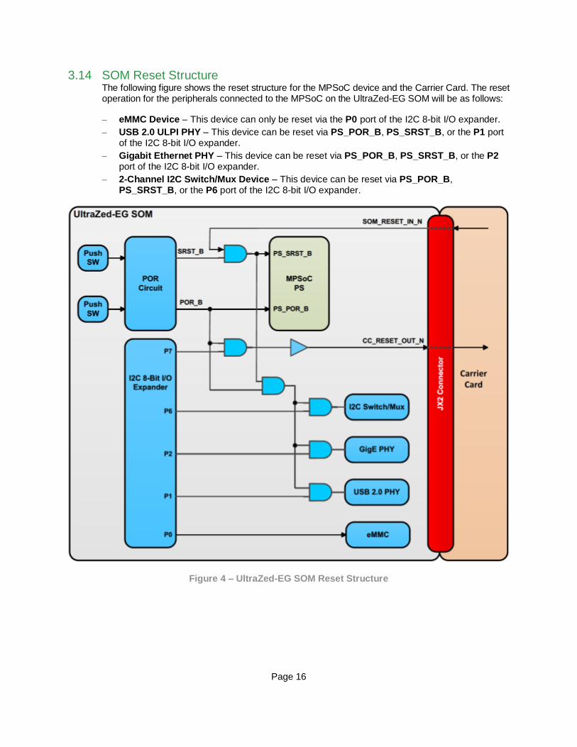
3.14 SOM Reset Structure The following figure shows the reset structure for the MPSoC device and the Carrier Card. The reset operation for the peripherals connected to the MPSoC on the UltraZed-EG SOM will be as follows:
– eMMC Device – This device can only be reset via the P0 port of the I2C 8-bit I/O expander.
– USB 2.0 ULPI PHY – This device can be reset via PS_POR_B, PS_SRST_B, or the P1 port of the I2C 8-bit I/O expander.
– Gigabit Ethernet PHY – This device can be reset via PS_POR_B, PS_SRST_B, or the P2 port of the I2C 8-bit I/O expander.
– 2-Channel I2C Switch/Mux Device – This device can be reset via PS_POR_B, PS_SRST_B, or the P6 port of the I2C 8-bit I/O expander.
Figure 4 – UltraZed-EG SOM Reset Structure
Page 17
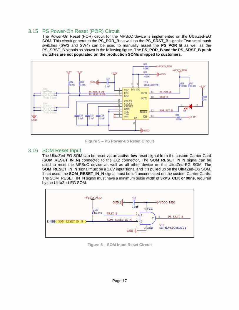
3.15 PS Power-On Reset (POR) Circuit The Power-On Reset (POR) circuit for the MPSoC device is implemented on the UltraZed-EG SOM. This circuit generates the PS_POR_B as well as the PS_SRST_B signals. Two small push switches (SW3 and SW4) can be used to manually assert the PS_POR_B as well as the PS_SRST_B signals as shown in the following figure. The PS_POR_B and the PS_SRST_B push switches are not populated on the production SOMs shipped to customers.
Figure 5 – PS Power-up Reset Circuit
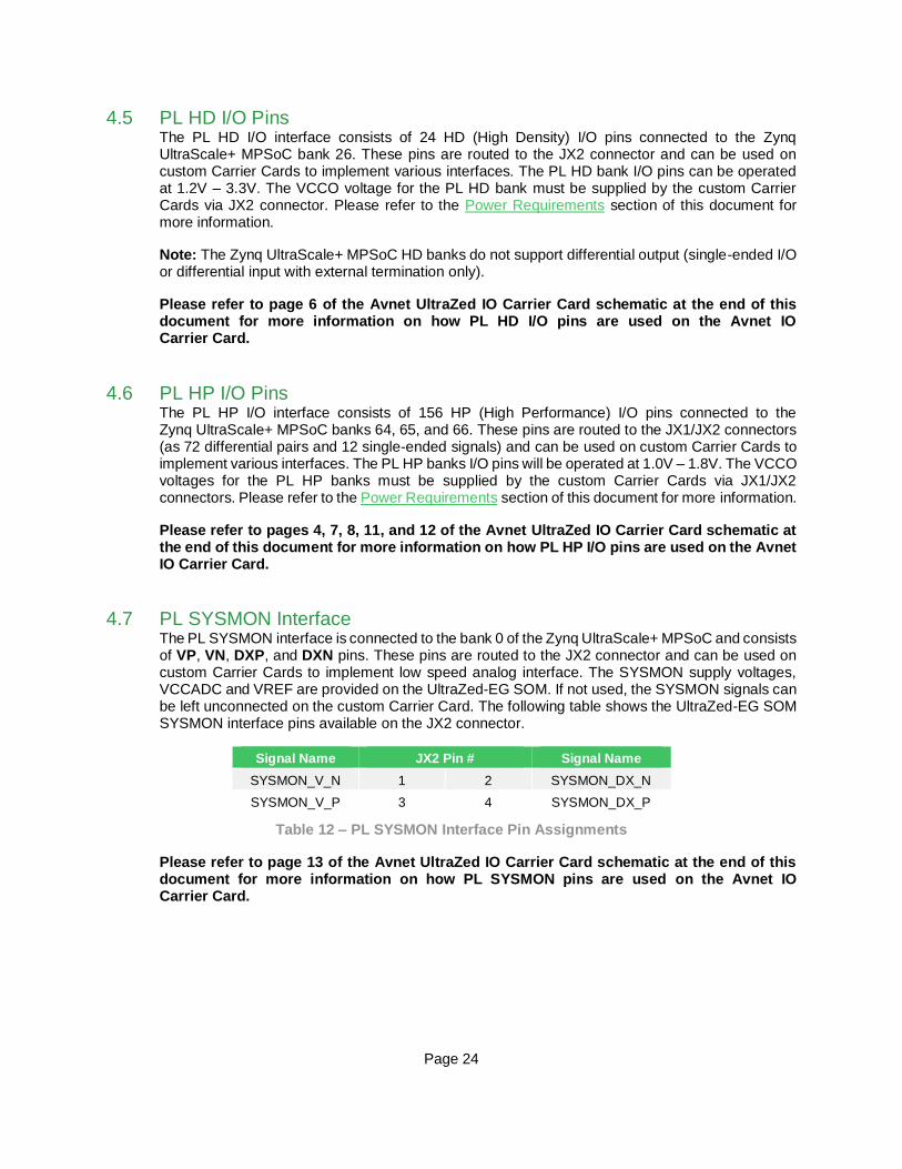
3.16 SOM Reset Input The UltraZed-EG SOM can be reset via an active low reset signal from the custom Carrier Card (SOM_RESET_IN_N) connected to the JX2 connector. The SOM_RESET_IN_N signal can be used to reset the MPSoC device as well as all other device on the UltraZed-EG SOM. The SOM_RESET_IN_N signal must be a 1.8V input signal and it is pulled up on the UltraZed-EG SOM. If not used, the SOM_RESET_IN_N signal must be left unconnected on the custom Carrier Cards. The SOM_RESET_IN_N signal must have a minimum pulse width of 3xPS_CLK or 90ns, required by the UltraZed-EG SOM.
Figure 6 – SOM Input Reset Circuit
Page 18
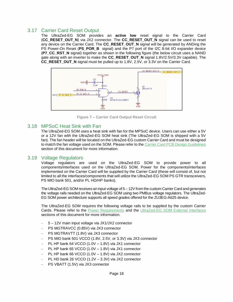
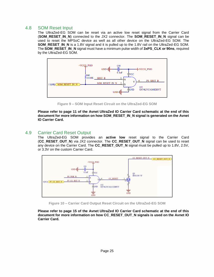
3.17 Carrier Card Reset Output The UltraZed-EG SOM provides an active low reset signal to the Carrier Card (CC_RESET_OUT_N) via JX2 connector. The CC_RESET_OUT_N signal can be used to reset any device on the Carrier Card. The CC_RESET_OUT_N signal will be generated by ANDing the PS Power-On Reset (PS_POR_B signal) and the P7 port of the I2C 8-bit I/O expander device (P7_CC_RST_N signal) together as shown in the following figure (the below circuit uses a NAND gate along with an inverter to make the CC_RESET_OUT_N signal 1.8V/2.5V/3.3V capable). The CC_RESET_OUT_N signal must be pulled up to 1.8V, 2.5V, or 3.3V on the Carrier Card.
Figure 7 – Carrier Card Output Reset Circuit
3.18 MPSoC Heat Sink with Fan The UltraZed-EG SOM uses a heat sink with fan for the MPSoC device. Users can use either a 5V or a 12V fan with the UltraZed-EG SOM heat sink (The UltraZed-EG SOM is shipped with a 5V fan). The fan header will be located on the UltraZed-EG custom Carrier Card and must be designed to match the fan voltage used on the SOM. Please refer to the Carrier Card PCB Design Guidelines section of this document for more information.
3.19 Voltage Regulators Voltage regulators are used on the UltraZed-EG SOM to provide power to all components/interfaces used on the UltraZed-EG SOM. Power for the components/interfaces implemented on the Carrier Card will be supplied by the Carrier Card (these will consist of, but not limited to all the interfaces/components that will utilize the UltraZed-EG SOM PS GTR transceivers, PS MIO bank 501, and/or PL HD/HP banks).
The UltraZed-EG SOM receives an input voltage of 5 – 12V from the custom Carrier Card and generates the voltage rails needed on the UltraZed-EG SOM using two PMBus voltage regulators. The UltraZed-EG SOM power architecture supports all speed grades offered for the ZU3EG-A625 device.
The UltraZed-EG SOM requires the following voltage rails to be supplied by the custom Carrier Cards. Please refer to the Power Requirements and the UltraZed-EG SOM External Interfaces sections of this document for more information.
– 5 – 12V main input voltage via JX1/JX2 connector
– PS MGTRAVCC (0.85V) via JX3 connector
– PS MGTRAVTT (1.8V) via JX3 connector
– PS MIO bank 501 VCCO (1.8V, 2.5V, or 3.3V) via JX3 connector
– PL HP bank 64 VCCO (1.0V – 1.8V) via JX1 connector
– PL HP bank 65 VCCO (1.0V – 1.8V) via JX1 connector
– PL HP bank 66 VCCO (1.0V – 1.8V) via JX2 connector
– PL HD bank 26 VCCO (1.2V – 3.3V) via JX2 connector
– PS VBATT (1.5V) via JX3 connector
Page 19
4 UltraZed-EG SOM External Interfaces The UltraZed-EG SOM provides sufficient resources to the custom Carrier Cards to implement fully customized systems that meet their application requirements. The UltraZed-EG SOM provides the following external interfaces to the custom Carrier Cards (signal directions are with respect to the UltraZed-EG SOM):
– 26 PS MIO pins (PS MIO bank 501, MIO[26:51])
– 4 PS GTR transceivers
– 4 PS GTR reference clock inputs
– PS JTAG interface
– PL SYSMON interface
– PMBus interface
– Carrier Card I2C interface
– SOM Reset input
– Carrier Card interrupt input
– Carrier Card Reset output
– USB 2.0 connector interface
– Gigabit Ethernet RJ45 connector interface
– 24 PL HD (High Density) I/O pins (1 bank)
– 156 PL HP (High Performance) I/O pins (3 banks)
– SOM PS VBATT input
– SOM Power Good output
– SOM input power The 4 PS GTR transceivers along with the 4 GTR reference clock inputs available via UltraZed-EG SOM JX3 connector can be used to implement the following interfaces on the custom Carrier Cards:
– USB 3.0 interface
– PCIe Endpoint or Root Port interface
– SATA Host interface
– Display Port interface The 26 PS Multiplexed I/O (MIO) pins available via UltraZed-EG SOM JX3 connector can be used to
– SD card interface
– CAN, UART, I2C, SPI interfaces
– General-purpose I/O (GPIO) The PL HD and HP general-purpose I/O pins can be used to implement a variety of interfaces on the custom Carrier Cards. Please refer to the Avnet UltraZed IO Carrier Card Users Guide on the www.ultrazed.org/product/ultrazed-io-carrier-card website for examples of interfaces implemented using the PL HD and HP I/O pins.
Page 20
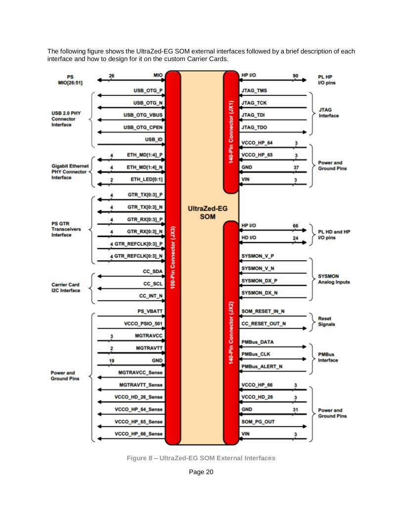
The following figure shows the UltraZed-EG SOM external interfaces followed by a brief description of each interface and how to design for it on the custom Carrier Cards.
Figure 8 – UltraZed-EG SOM External Interfaces
Page 21
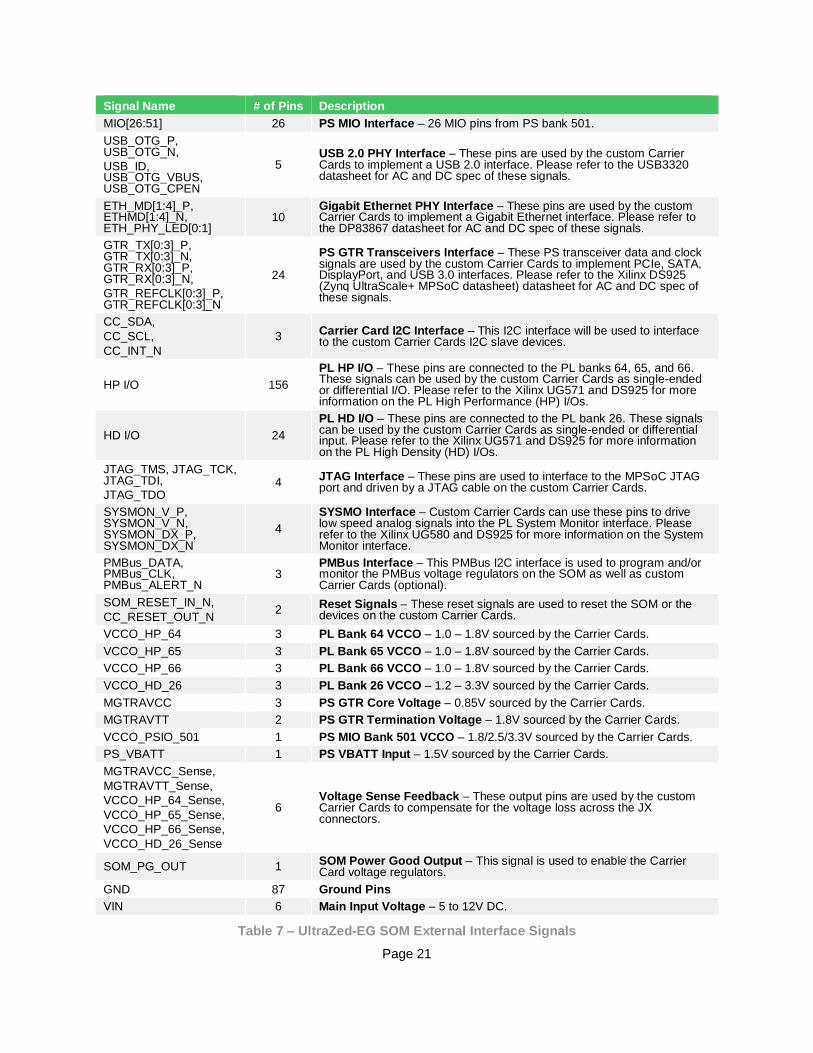
Signal Name # of Pins Description
MIO[26:51] 26 PS MIO Interface – 26 MIO pins from PS bank 501.
USB_OTG_P, USB_OTG_N,
USB_ID, USB_OTG_VBUS, USB_OTG_CPEN
5 USB 2.0 PHY Interface – These pins are used by the custom Carrier Cards to implement a USB 2.0 interface. Please refer to the USB3320 datasheet for AC and DC spec of these signals.
ETH_MD[1:4]_P, ETHMD[1:4]_N, ETH_PHY_LED[0:1]
10 Gigabit Ethernet PHY Interface – These pins are used by the custom Carrier Cards to implement a Gigabit Ethernet interface. Please refer to the DP83867 datasheet for AC and DC spec of these signals.
GTR_TX[0:3]_P, GTR_TX[0:3]_N, GTR_RX[0:3]_P, GTR_RX[0:3]_N,
GTR_REFCLK[0:3]_P, GTR_REFCLK[0:3]_N
24
PS GTR Transceivers Interface – These PS transceiver data and clock signals are used by the custom Carrier Cards to implement PCIe, SATA, DisplayPort, and USB 3.0 interfaces. Please refer to the Xilinx DS925 (Zynq UltraScale+ MPSoC datasheet) datasheet for AC and DC spec of these signals.
CC_SDA,
CC_SCL,
CC_INT_N
3 Carrier Card I2C Interface – This I2C interface will be used to interface to the custom Carrier Cards I2C slave devices.
HP I/O 156
PL HP I/O – These pins are connected to the PL banks 64, 65, and 66. These signals can be used by the custom Carrier Cards as single-ended or differential I/O. Please refer to the Xilinx UG571 and DS925 for more information on the PL High Performance (HP) I/Os.
HD I/O 24
PL HD I/O – These pins are connected to the PL bank 26. These signals can be used by the custom Carrier Cards as single-ended or differential input. Please refer to the Xilinx UG571 and DS925 for more information on the PL High Density (HD) I/Os.
JTAG_TMS, JTAG_TCK, JTAG_TDI,
JTAG_TDO 4
JTAG Interface – These pins are used to interface to the MPSoC JTAG port and driven by a JTAG cable on the custom Carrier Cards.
SYSMON_V_P, SYSMON_V_N, SYSMON_DX_P, SYSMON_DX_N
4
SYSMO Interface – Custom Carrier Cards can use these pins to drive low speed analog signals into the PL System Monitor interface. Please refer to the Xilinx UG580 and DS925 for more information on the System Monitor interface.
PMBus_DATA, PMBus_CLK, PMBus_ALERT_N
3 PMBus Interface – This PMBus I2C interface is used to program and/or monitor the PMBus voltage regulators on the SOM as well as custom Carrier Cards (optional).
SOM_RESET_IN_N,
CC_RESET_OUT_N 2
Reset Signals – These reset signals are used to reset the SOM or the devices on the custom Carrier Cards.
VCCO_HP_64 3 PL Bank 64 VCCO – 1.0 – 1.8V sourced by the Carrier Cards.
VCCO_HP_65 3 PL Bank 65 VCCO – 1.0 – 1.8V sourced by the Carrier Cards.
VCCO_HP_66 3 PL Bank 66 VCCO – 1.0 – 1.8V sourced by the Carrier Cards.
VCCO_HD_26 3 PL Bank 26 VCCO – 1.2 – 3.3V sourced by the Carrier Cards.
MGTRAVCC 3 PS GTR Core Voltage – 0.85V sourced by the Carrier Cards.
MGTRAVTT 2 PS GTR Termination Voltage – 1.8V sourced by the Carrier Cards.
VCCO_PSIO_501 1 PS MIO Bank 501 VCCO – 1.8/2.5/3.3V sourced by the Carrier Cards.
PS_VBATT 1 PS VBATT Input – 1.5V sourced by the Carrier Cards.
MGTRAVCC_Sense,
MGTRAVTT_Sense,
VCCO_HP_64_Sense,
VCCO_HP_65_Sense,
VCCO_HP_66_Sense,
VCCO_HD_26_Sense
6 Voltage Sense Feedback – These output pins are used by the custom Carrier Cards to compensate for the voltage loss across the JX connectors.
SOM_PG_OUT 1 SOM Power Good Output – This signal is used to enable the Carrier Card voltage regulators.
GND 87 Ground Pins
VIN 6 Main Input Voltage – 5 to 12V DC.
Table 7 – UltraZed-EG SOM External Interface Signals
Page 22
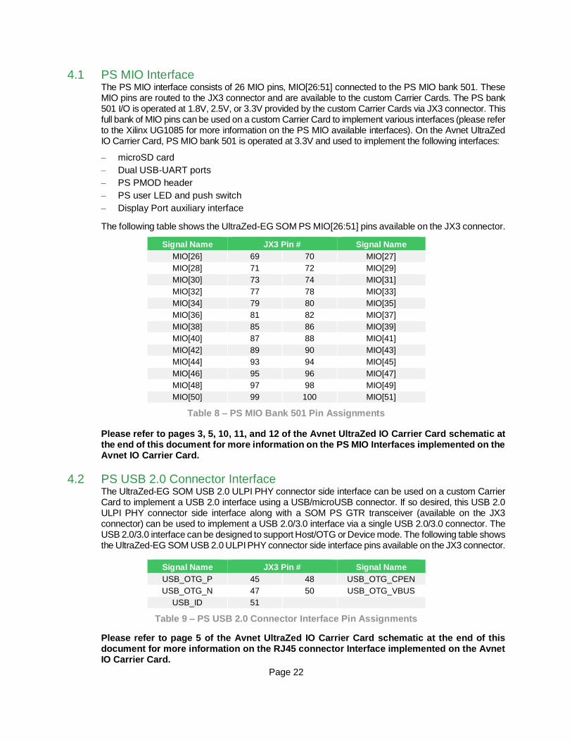
4.1 PS MIO Interface The PS MIO interface consists of 26 MIO pins, MIO[26:51] connected to the PS MIO bank 501. These MIO pins are routed to the JX3 connector and are available to the custom Carrier Cards. The PS bank 501 I/O is operated at 1.8V, 2.5V, or 3.3V provided by the custom Carrier Cards via JX3 connector. This full bank of MIO pins can be used on a custom Carrier Card to implement various interfaces (please refer to the Xilinx UG1085 for more information on the PS MIO available interfaces). On the Avnet UltraZed IO Carrier Card, PS MIO bank 501 is operated at 3.3V and used to implement the following interfaces:
– microSD card
– Dual USB-UART ports
– PS PMOD header
– PS user LED and push switch
– Display Port auxiliary interface
The following table shows the UltraZed-EG SOM PS MIO[26:51] pins available on the JX3 connector.
Signal Name JX3 Pin # Signal Name
MIO[26] 69 70 MIO[27]
MIO[28] 71 72 MIO[29]
MIO[30] 73 74 MIO[31]
MIO[32] 77 78 MIO[33]
MIO[34] 79 80 MIO[35]
MIO[36] 81 82 MIO[37]
MIO[38] 85 86 MIO[39]
MIO[40] 87 88 MIO[41]
MIO[42] 89 90 MIO[43]
MIO[44] 93 94 MIO[45]
MIO[46] 95 96 MIO[47]
MIO[48] 97 98 MIO[49]
MIO[50] 99 100 MIO[51]
Table 8 – PS MIO Bank 501 Pin Assignments
Please refer to pages 3, 5, 10, 11, and 12 of the Avnet UltraZed IO Carrier Card schematic at the end of this document for more information on the PS MIO Interfaces implemented on the Avnet IO Carrier Card.
4.2 PS USB 2.0 Connector Interface The UltraZed-EG SOM USB 2.0 ULPI PHY connector side interface can be used on a custom Carrier Card to implement a USB 2.0 interface using a USB/microUSB connector. If so desired, this USB 2.0 ULPI PHY connector side interface along with a SOM PS GTR transceiver (available on the JX3 connector) can be used to implement a USB 2.0/3.0 interface via a single USB 2.0/3.0 connector. The USB 2.0/3.0 interface can be designed to support Host/OTG or Device mode. The following table shows the UltraZed-EG SOM USB 2.0 ULPI PHY connector side interface pins available on the JX3 connector.
Signal Name JX3 Pin # Signal Name
USB_OTG_P 45 48 USB_OTG_CPEN
USB_OTG_N 47 50 USB_OTG_VBUS
USB_ID 51
Table 9 – PS USB 2.0 Connector Interface Pin Assignments
Please refer to page 5 of the Avnet UltraZed IO Carrier Card schematic at the end of this document for more information on the RJ45 connector Interface implemented on the Avnet IO Carrier Card.
Page 23
4.3 PS RJ45 Connector Interface The UltraZed-EG SOM Gigabit Ethernet PHY connector side interface along with an RJ45 connector on the custom Carrier Card can be used to implement a single Gigabit Ethernet port. The following table shows the UltraZed-EG SOM Gigabit Ethernet PHY connector side interface pins available on the JX3 connector.
Signal Name JX3 Pin # Signal Name
ETH_PHY_LED0 53 70 ETH_PHY_LED1
ETH_MD1_P 57 72 ETH_MD2_P
ETH_MD1_N 59 74 ETH_MD2_N
ETH_MD3_P 63 78 ETH_MD4_P
ETH_MD3_N 65 80 ETH_MD4_N
Table 10 – PS RJ45 Connector Interface Pin Assignments
Please refer to page 5 of the Avnet UltraZed IO Carrier Card schematic at the end of this document for more information on the RJ45 connector Interface implemented on the Avnet IO Carrier Card.
4.4 PS GTR Transceiver Interface The UltraZed-EG SOM provides 4 PS GTR transceivers along with 4 GTR reference clock inputs to the custom Carrier Cards via the JX3 connector. These 4 transceivers can be used on a custom Carrier Card to implement USB 3.0, Display Port, SATA host, and PCIe interfaces. Please refer to the UG1085 (Zynq UltraScale+ Technical Reference Manual) for more information on how each GTR transceiver can be used in a design.
The GTR transceiver power (0.85V and 1.8V rails) must be supplied by the custom Carrier Card via JX3 connector. Please refer to the Power Requirements section of this document for more information. The following table shows the UltraZed-EG SOM PS GTR and GTR reference clock input pins available on the JX3 connector.
Signal Name JX3 Pin # Signal Name
GTR_TX3_P 1 4 GTR_RX3_P
GTR_TX3_N 3 6 GTR_RX3_N
GTR_TX2_P 7 10 GTR_RX2_P
GTR_TX2_N 9 12 GTR_RX2_N
GTR_TX1_P 13 18 GTR_RX1_P
GTR_TX1_N 15 20 GTR_RX1_N
GTR_TX0_P 21 26 GTR_RX0_P
GTR_TX0_N 23 28 GTR_RX0_N
GTR_REFCLK3_P 27 32 GTR_REFCLK2_P
GTR_REFCLK3_N 29 34 GTR_REFCLK2_N
GTR_REFCLK1_P 33 38 GTR_REFCLK0_P
GTR_REFCLK1_N 35 40 GTR_REFCLK0_N
Table 11 – PS GTR Interface Pin Assignments
Please refer to pages 3, 4, 5, and 16 of the Avnet UltraZed IO Carrier Card schematic at the end of this document for more information on how PS GTR interfaces are implemented on the Avnet IO Carrier Card.
Page 24
4.5 PL HD I/O Pins The PL HD I/O interface consists of 24 HD (High Density) I/O pins connected to the Zynq UltraScale+ MPSoC bank 26. These pins are routed to the JX2 connector and can be used on custom Carrier Cards to implement various interfaces. The PL HD bank I/O pins can be operated at 1.2V – 3.3V. The VCCO voltage for the PL HD bank must be supplied by the custom Carrier Cards via JX2 connector. Please refer to the Power Requirements section of this document for more information.
Note: The Zynq UltraScale+ MPSoC HD banks do not support differential output (single-ended I/O or differential input with external termination only).
Please refer to page 6 of the Avnet UltraZed IO Carrier Card schematic at the end of this document for more information on how PL HD I/O pins are used on the Avnet IO Carrier Card.
4.6 PL HP I/O Pins The PL HP I/O interface consists of 156 HP (High Performance) I/O pins connected to the Zynq UltraScale+ MPSoC banks 64, 65, and 66. These pins are routed to the JX1/JX2 connectors (as 72 differential pairs and 12 single-ended signals) and can be used on custom Carrier Cards to implement various interfaces. The PL HP banks I/O pins will be operated at 1.0V – 1.8V. The VCCO voltages for the PL HP banks must be supplied by the custom Carrier Cards via JX1/JX2 connectors. Please refer to the Power Requirements section of this document for more information.
Please refer to pages 4, 7, 8, 11, and 12 of the Avnet UltraZed IO Carrier Card schematic at the end of this document for more information on how PL HP I/O pins are used on the Avnet IO Carrier Card.
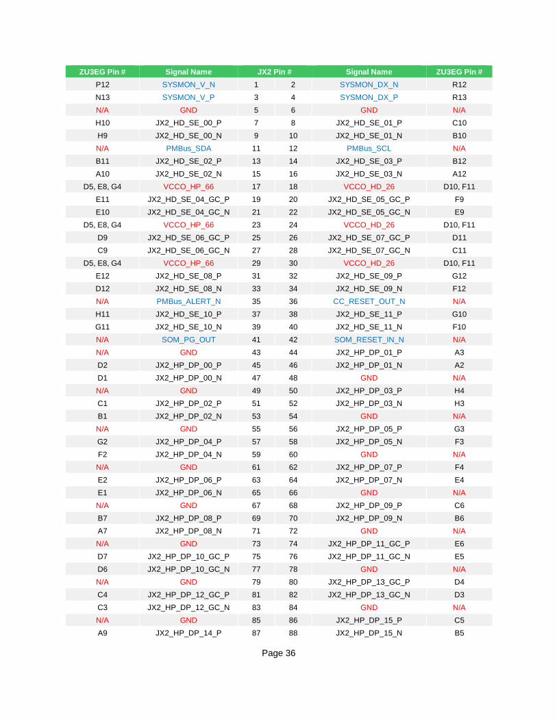
4.7 PL SYSMON Interface The PL SYSMON interface is connected to the bank 0 of the Zynq UltraScale+ MPSoC and consists of VP, VN, DXP, and DXN pins. These pins are routed to the JX2 connector and can be used on custom Carrier Cards to implement low speed analog interface. The SYSMON supply voltages, VCCADC and VREF are provided on the UltraZed-EG SOM. If not used, the SYSMON signals can be left unconnected on the custom Carrier Card. The following table shows the UltraZed-EG SOM SYSMON interface pins available on the JX2 connector.
Signal Name JX2 Pin # Signal Name
SYSMON_V_N 1 2 SYSMON_DX_N
SYSMON_V_P 3 4 SYSMON_DX_P
Table 12 – PL SYSMON Interface Pin Assignments
Please refer to page 13 of the Avnet UltraZed IO Carrier Card schematic at the end of this document for more information on how PL SYSMON pins are used on the Avnet IO Carrier Card.
Page 25
4.8 SOM Reset Input The UltraZed-EG SOM can be reset via an active low reset signal from the Carrier Card (SOM_RESET_IN_N) connected to the JX2 connector. The SOM_RESET_IN_N signal can be used to reset the MPSoC device as well as all other device on the UltraZed-EG SOM. The SOM_RESET_IN_N is a 1.8V signal and it is pulled up to the 1.8V rail on the UltraZed-EG SOM. The SOM_RESET_IN_N signal must have a minimum pulse width of 3xPS_CLK or 90ns, required by the UltraZed-EG SOM.
Figure 9 – SOM Input Reset Circuit on the UltraZed-EG SOM
Please refer to page 11 of the Avnet UltraZed IO Carrier Card schematic at the end of this document for more information on how SOM_RESET_IN_N signal is generated on the Avnet IO Carrier Card.
4.9 Carrier Card Reset Output The UltraZed-EG SOM provides an active low reset signal to the Carrier Card (CC_RESET_OUT_N) via JX2 connector. The CC_RESET_OUT_N signal can be used to reset any device on the Carrier Card. The CC_RESET_OUT_N signal must be pulled up to 1.8V, 2.5V, or 3.3V on the custom Carrier Card.
Figure 10 – Carrier Card Output Reset Circuit on the UltraZed-EG SOM
Please refer to page 15 of the Avnet UltraZed IO Carrier Card schematic at the end of this document for more information on how CC_RESET_OUT_N signals is used on the Avnet IO Carrier Card.
Page 26
4.10 Carrier Card I2C Interface The UltraZed-EG SOM provides a master I2C bus (CC_SDA, CC_SCL, and CC_INT_N) to the Carrier Card via the JX3 connector so that software can communicate with all I2C devices on the UltraZed-EG SOM as well as the slave I2C devices on the Carrier Card using a single I2C interface. The CC_SDA, CC_SCL, and CC_INT_N pins must be pulled up to the 1.8V, 2.5V, or 3.3V on the Carrier Card.
The Carrier Card I2C interface is connected to the channel 0 of the I2C 2-channel switch/mux device on the UltraZed-EG SOM. Carrier Cards can drive the INT0 of the channel 0 via CC_INT_N, if they so desire. The CC_INT_N signal is not specific to the I2C interface and can be used as a general-purpose interrupt from Carrie Cards to the UltraZed-EG SOM. If not used, the CC_INT_N signal must be pulled up to 1.8V, 2.5V, or 3.3V on the Carrier Card. Since channel 0 I2C bus is dedicated to the Carrier Card, I2C devices with any address can reside on this bus without conflicting with the I2C devices on the UltraZed-EG SOM. The following table shows the UltraZed-EG SOM Carrier Card I2C interface pins available on the JX3 connector.
Signal Name JX3 Pin # Signal Name
CC_SDA 41 44 CC_SCL
68 CC_INT_N
Table 13 – Carrier Card I2C Interface Pin Assignments
Please refer to pages 4 and 5 of the Avnet UltraZed IO Carrier Card schematic at the end of this document for more information on how Carrier Card I2C is used on the Avnet IO Carrier Card.
4.11 Ethernet MAC ID A MAC Address device such as the Microchip 24AA025E48T-I/OT device can be used on the custom Carrier Card. This device can be connected to the Carrier Card I2C interface (CC_SDA and CC_SCL).
Please refer to page 5 of the Avnet UltraZed IO Carrier Card schematic at the end of this document for more information on how the MAC ID is implemented on the Avnet IO Carrier Card.
Page 27
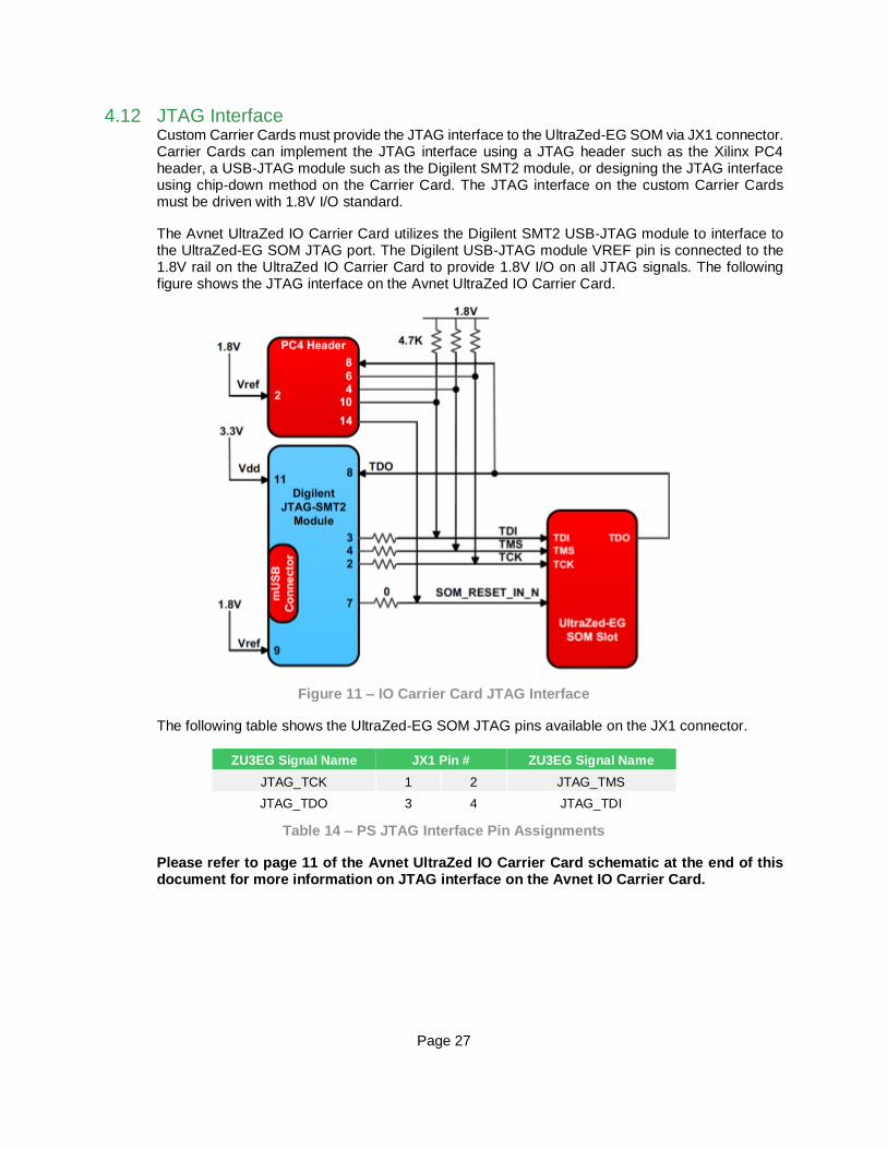
4.12 JTAG Interface Custom Carrier Cards must provide the JTAG interface to the UltraZed-EG SOM via JX1 connector. Carrier Cards can implement the JTAG interface using a JTAG header such as the Xilinx PC4 header, a USB-JTAG module such as the Digilent SMT2 module, or designing the JTAG interface using chip-down method on the Carrier Card. The JTAG interface on the custom Carrier Cards must be driven with 1.8V I/O standard.
The Avnet UltraZed IO Carrier Card utilizes the Digilent SMT2 USB-JTAG module to interface to the UltraZed-EG SOM JTAG port. The Digilent USB-JTAG module VREF pin is connected to the 1.8V rail on the UltraZed IO Carrier Card to provide 1.8V I/O on all JTAG signals. The following figure shows the JTAG interface on the Avnet UltraZed IO Carrier Card.
Figure 11 – IO Carrier Card JTAG Interface
The following table shows the UltraZed-EG SOM JTAG pins available on the JX1 connector.
ZU3EG Signal Name JX1 Pin # ZU3EG Signal Name
JTAG_TCK 1 2 JTAG_TMS
JTAG_TDO 3 4 JTAG_TDI
Table 14 – PS JTAG Interface Pin Assignments
Please refer to page 11 of the Avnet UltraZed IO Carrier Card schematic at the end of this document for more information on JTAG interface on the Avnet IO Carrier Card.
Page 28
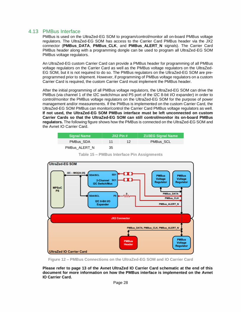
4.13 PMBus Interface PMBus is used on the UltraZed-EG SOM to program/control/monitor all on-board PMBus voltage regulators. The UltraZed-EG SOM has access to the Carrier Card PMBus header via the JX2 connector (PMBus_DATA, PMBus_CLK, and PMBus_ALERT_N signals). The Carrier Card PMBus header along with a programming dongle can be used to program all UltraZed-EG SOM PMBus voltage regulators.
An UltraZed-EG custom Carrier Card can provide a PMBus header for programming of all PMBus voltage regulators on the Carrier Card as well as the PMBus voltage regulators on the UltraZed-EG SOM, but it is not required to do so. The PMBus regulators on the UltraZed-EG SOM are pre-programmed prior to shipment. However, if programming of PMBus voltage regulators on a custom Carrier Card is required, the custom Carrier Card must implement the PMBus header.
After the initial programming of all PMBus voltage regulators, the UltraZed-EG SOM can drive the PMBus (via channel 1 of the I2C switch/mux and P5 port of the I2C 8-bit I/O expander) in order to control/monitor the PMBus voltage regulators on the UltraZed-EG SOM for the purpose of power management and/or measurements. If the PMBus is implemented on the custom Carrier Card, the UltraZed-EG SOM PMBus can monitor/control the Carrier Card PMBus voltage regulators as well. If not used, the UltraZed-EG SOM PMBus interface must be left unconnected on custom Carrier Cards so that the UltraZed-EG SOM can still control/monitor its on-board PMBus regulators. The following figure shows how the PMBus is connected on the UltraZed-EG SOM and the Avnet IO Carrier Card.
Signal Name JX2 Pin # ZU3EG Signal Name
PMBus_SDA 11 12 PMBus_SCL
PMBus_ALERT_N 35
Table 15 – PMBus Interface Pin Assignments
Figure 12 – PMBus Connections on the UltraZed-EG SOM and IO Carrier Card
Please refer to page 13 of the Avnet UltraZed IO Carrier Card schematic at the end of this document for more information on how the PMBus interface is implemented on the Avnet IO Carrier Card.
Page 29
4.14 Power Requirements The UltraZed-EG SOM requires the following rails to be supplied by the Carrier Card. In return, the UltraZed-EG SOM will provide a voltage sense feedback for each rail (with the exception of the 5 – 12V input voltage and the PS MIO bank 501 VCCO) to the Carrier Card via JX connectors (please refer to section 5 of this document for the JX1, JX2, and JX3 detail pinout information). The voltage sense feedback for each rail can be used by the regulator on the Carrier Card to compensate for the voltage loss across the JX connectors. Please refer to the DS925 (Zynq UltraScale+ MPSoC datasheet) for percent variation on all the following voltage rails when designing the power system for the custom Carrier Card. The custom Carrier Cards are required to supply the following rails to the UltraZed-EG SOM:
– 5 – 12V main input voltage via JX1/JX2 connectors
– PS MGTRAVCC (0.85V) via JX3 connector
– PS MGTRAVTT (1.8V) via JX3 connector
– PS MIO bank 501 VCCO (1.8V, 2.5V, or 3.3V) via JX3 connector
– PL HP bank 64 VCCO (1.0V – 1.8V) via JX1 connector
– PL HP bank 65 VCCO (1.0V – 1.8V) via JX1 connector
– PL HP bank 66 VCCO (1.0V – 1.8V) via JX2 connector
– PL HD bank 26 VCCO (1.2V – 3.3V) via JX2 connector
– PS VBATT (1.5V) via JX3 connector
Voltage Rail Name Voltage Value Current Requirement Voltage Sense Feedback
VIN 5 – 12V 3.6A @ 5V or 1.5A @ 12V NA
MGTRAVCC 0.85V 1A MGTRAVCC_Sense
MGTRAVTT 1.8V 1A MGTRAVTT_Sense
VCCO_PSIO_501 1.8V, 2.5V, or 3.3V 0.5A NA
VCCO_HP_64 1.0V – 1.8V 1A VCCO_HP_64_Sense
VCCO_HP_65 1.0V – 1.8V 1A VCCO_HP_65_Sense
VCCO_HP_66 1.0V – 1.8V 1A VCCO_HP_66_Sense
VCCO_HD_26 1.2V – 3.3V 0.5A VCCO_HD_26_Sense
PS_VBATT 1.5V 250nA NA
Table 16 – UltraZed-EG SOM Power Requirements
Some of the above voltage rails can be combined to reduce the cost of power supply design on the custom Carrier Card. The MGTRAVCC and MGTRAVTT analog voltage rails should not be combined with any VCCO rails.
On the Avnet UltraZed IO Carrier Card, all PL HP bank VCCOs are driven with a single 1.8V supply. The PL HD bank VCCO and PS MIO bank 501 VCCO are driven with a single 3.3V supply. The following lists the regulated voltage rails generated by a single PMBus voltage regulator on the UltraZed IO Carrier Card for the UltraZed-EG SOM.
– 0.85V for the MGTRAVCC via JX3
– 1.8V for the MGTRAVTT via JX3
– 1.8V for all PL HP banks via JX1/JX2
– 3.3V for the PL HD bank and PS MIO bank 501 via JX2/JX3
Page 30
4.15 Power Sequencing Proper power sequencing is needed for the following rails supplied to the UltraZed-EG SOM by the Carrier Cards:
– PS MGTRAVCC
– PS MGTRAVTT
– PS MIO bank 501 VCCO
– PL HP bank 64 VCCO
– PL HP bank 65 VCCO
– PL HP bank 66 VCCO
– PL HD bank 26 VCCO
The SOM_PG_OUT signal from the UltraZed-EG SOM (3.3V signal, connected to the JX2 connector) must be used to assist in power sequencing. The Carrier Card voltage regulator(s) should not be turned ON until the SOM_PG_OUT signal is asserted.
In order to boot from a device on the custom Carrier Card (such as booting from the microSD/SD Card), all power rails on the custom Carrier Card must be stable within 300ms of the SOM_PG_OUT assertion. This will ensure all custom Carrier Card power rails are up and stable before the PS_POR_B signal is de-asserted and the MPSoC boot execution is initiated on the UltraZed-EG SOM. The power rails on the Avnet IO Carrier Card are up and stable less than 100ms from the SOM_PG_OUT assertion.
Please refer to page 14 of the Avnet UltraZed IO Carrier Card schematic at the end of this document for more information on how the SOM_PG_OUT is used on the Avnet IO Carrier Card.
Once the SOM_PG_OUT signal is asserted, the Carrier Card must turn on the above voltage rails in the following sequence (the reverse sequence must be maintained on turn off):
1. PS MGTRAVCC rail followed by the PS MGTRAVTT rail.
2. PS bank 501 and PL banks 26, 64, 65, and 66 VCCO in any sequence before or after the MGTRAVCC/ MGTRAVTT rails.
4.16 Power Estimation Using XPE Xilinx Power Estimator (XPE) should be used to generate worst case power estimations for selecting power devices for the I/O banks. The Xilinx Power Estimator (XPE) spreadsheet is available on Xilinx’ website that can help you get started with your own power estimation. You may download this file and add or modify your desired PL utilization to provide a worst case estimation for your own VCCO supplies.
4.17 MPSoC Heat Sink with Fan The UltraZed-EG SOM uses a heat sink with fan for the MPSoC device. Users can use either a 5V or a 12V fan with the UltraZed-EG SOM heat sink (The UltraZed-EG SOM is shipped with a 5V fan). The fan header will be located on the UltraZed-EG custom Carrier Card and must be designed to match the fan voltage used on the SOM. Please refer to the Carrier Card PCB Design Guidelines section of this document for more information.
Please refer to page 15 of the Avnet UltraZed IO Carrier Card schematic at the end of this document for more information on how the Fan Header is implemented on the Avnet IO Carrier Card.
Page 31
5 UltraZed-EG SOM JX Micro Connectors The UltraZed-EG SOM utilizes 3 micro headers to provide connections to the Carrier Card. TE 0.8mm FH (Free Height) connectors are used to implement the UltraZed-EG SOM to the Carrier Card connections. The UltraZed-EG SOM uses a 100-pin (JX3), and two 140-pin (JX1 and JX2) plug connectors. These connectors carry the following signals and power/ground pins (signal directions are with respect to the UltraZed-EG SOM):
– JX1 Connector (140-pin Plug, TE part number: 2-5177986-6)
– JTAG pins (JTAG_TMS, JTAG_TCK, JTAG_TDI, and JTAG_TDO)
– 42 differential HP I/O pairs (JX1_HP_DP)
– 6 single ended signals (JX1_HP_SE)
– Power and ground pins (VCCO_HP_64, VCCO_HP_65, VIN, and GND)
– JX2 Connector (140-pin Plug, TE part number: 2-5177986-6)
– SYSMON pins (SYSMON_V_P, SYSMON_V_N, SYSMON_DX_P, and SYSMON_DX_N)
– 30 differential HP I/O pairs (JX2_HP_DP), 30 single ended signals (JX2_HP_SE and JX2_HD_SE)
– Power and ground pins (VCCO_HP_66, VCCO_HD_26, VIN, and GND)
– SOM_RESET_IN_N input
– CC_RESET_OUT_N output
– SOM_PG_OUT output
– PMBus signals (PMBus_DATA, PMBus_CLK, and PMBus_ALERT_N)
– JX3 Connector (100-pin Plug, TE part number: 2-5177986-4)
– PS GTR[0:3], PS GTR_REFCLK[0:3]
– PS MIO bank 501 pins (MIO[26:51])
– USB 2.0 connector interface (USB_OTG_P, USB_OTG_N, USB_ID, USB_OTG_VBUS, and USB_OTG_CPEN)
– Gigabit Ethernet connector interface (ETH_MD[1:4]_P, ETHMD[1:4]_N, and ETH_PHY_LED[0:1])
– Carrier Card I2C interface (CC_SDA, CC_SCL, and CC_INT_N)
– PS_VBATT input
– Power and ground pins (MGTRAVCC, MGTRAVTT, and GND)
– Voltage sense feedback output pins (MGTRAVCC_Sense, MGTRAVCC_Sense, VCCO_HP_64_Sense, VCCO_HP_65_Sense, VCCO_HP_66_Sense, and VCCO_HD_26_Sense)
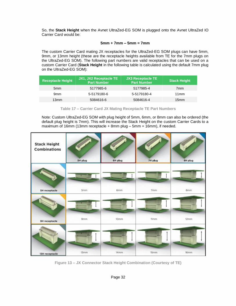
5.1 Custom Carrier Cards Mating JX Receptacle Connectors The JX1, JX2, and JX3 plugs on the Avnet UltraZed-EG SOM have a default height of 7mm. The height of the mating JX receptacles for the custom Carrier Cards must be selected such that the Stack Height is <= 16mm when the UltraZed-EG is plugged onto the custom Carrier Card (this requirement must be met in order to meet the 6Gbps data rate for the PS GTR transceivers connected to the JX3 connector). The Stack Height is calculated as follows:
Stack Height = Receptacle Height(mm) + Plug Height(mm) – 5mm
On the Avnet UltraZed IO Carrier Card , the JX1, JX2, and JX3 receptacles have 5mm height:
– JX1 Connector (140-pin Receptacle, TE part number: 5177985-6)
– JX2 Connector (140-pin Receptacle, TE part number: 5177985-6)
– JX3 Connector (100-pin Receptacle, TE part number: 5177985-4)
Page 32
So, the Stack Height when the Avnet UltraZed-EG SOM is plugged onto the Avnet UltraZed IO Carrier Card would be:
5mm + 7mm – 5mm = 7mm
The custom Carrier Card mating JX receptacles for the UltraZed-EG SOM plugs can have 5mm, 9mm, or 13mm height (these are the receptacle heights available from TE for the 7mm plugs on the UltraZed-EG SOM). The following part numbers are valid receptacles that can be used on a custom Carrier Card (Stack Height in the following table is calculated using the default 7mm plug on the UltraZed-EG SOM):
Receptacle Height JX1, JX2 Receptacle TE
Part Number JX3 Receptacle TE
Part Number Stack Height
5mm 5177985-6 5177985-4 7mm
9mm 5-5179180-6 5-5179180-4 11mm
13mm 5084616-6 5084616-4 15mm
Table 17 – Carrier Card JX Mating Receptacle TE Part Numbers
Note: Custom UltraZed-EG SOM with plug height of 5mm, 6mm, or 8mm can also be ordered (the default plug height is 7mm). This will increase the Stack Height on the custom Carrier Cards to a maximum of 16mm (13mm receptacle + 8mm plug – 5mm = 16mm), if needed.
Figure 13 – JX Connector Stack Height Combination (Courtesy of TE)
Page 33
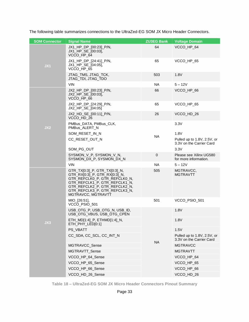
The following table summarizes connections to the UltraZed-EG SOM JX Micro Header Connectors.
SOM Connector Signal Name ZU3EG Bank Voltage Domain
JX1
JX1_HP_DP_[00:23]_P/N, JX1_HP_SE_[00:03], VCCO_HP_64
64 VCCO_HP_64
JX1_HP_DP_[24:41]_P/N, JX1_HP_SE_[04:05], VCCO_HP_65
65 VCCO_HP_65
JTAG_TMS, JTAG_TCK, JTAG_TDI, JTAG_TDO
503 1.8V
VIN NA 5 – 12V
JX2
JX2_HP_DP_[00:23]_P/N, JX2_HP_SE_[00:03], VCCO_HP_66
66 VCCO_HP_66
JX2_HP_DP_[24:29]_P/N, JX2_HP_SE_[04:05]
65 VCCO_HP_65
JX2_HD_SE_[00:11]_P/N, VCCO_HD_26
26 VCCO_HD_26
PMBus_DATA, PMBus_CLK, PMBus_ALERT_N
NA
3.3V
SOM_RESET_IN_N 1.8V
CC_RESET_OUT_N Pulled up to 1.8V, 2.5V, or 3.3V on the Carrier Card
SOM_PG_OUT 3.3V
SYSMON_V_P, SYSMON_V_N, SYSMON_DX_P, SYSMON_DX_N
0 Please see Xilinx UG580 for more information.
VIN NA 5 – 12V
JX3
GTR_TX[0:3]_P, GTR_TX[0:3]_N, GTR_RX[0:3]_P, GTR_RX[0:3]_N, GTR_REFCLK0_P, GTR_REFCLK0_N, GTR_REFCLK1_P, GTR_REFCLK1_N, GTR_REFCLK2_P, GTR_REFCLK2_N, GTR_REFCLK3_P, GTR_REFCLK3_N, MGTRAVCC, MGTRAVTT
505 MGTRAVCC, MGTRAVTT
MIO_[26:51], VCCO_PSIO_501
501 VCCO_PSIO_501
USB_OTG_P, USB_OTG_N, USB_ID, USB_OTG_VBUS, USB_OTG_CPEN
NA
1.8V
ETH_MD[1:4]_P, ETHMD[1:4]_N, ETH_PHY_LED[0:1]
1.8V
PS_VBATT 1.5V
CC_SDA, CC_SCL, CC_INT_N Pulled up to 1.8V, 2.5V, or 3.3V on the Carrier Card
MGTRAVCC_Sense MGTRAVCC
MGTRAVTT_Sense MGTRAVTT
VCCO_HP_64_Sense VCCO_HP_64
VCCO_HP_65_Sense VCCO_HP_65
VCCO_HP_66_Sense VCCO_HP_66
VCCO_HD_26_Sense VCCO_HD_26
Table 18 – UltraZed-EG SOM JX Micro Header Connectors Pinout Summary
Page 34
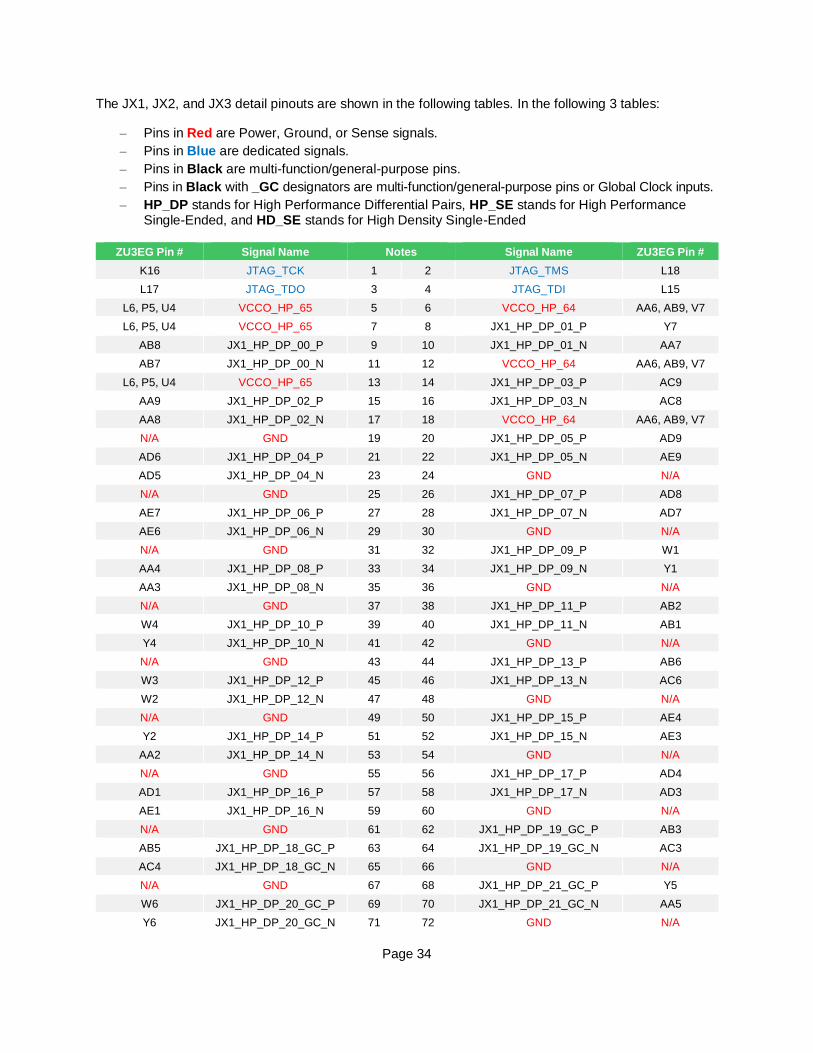
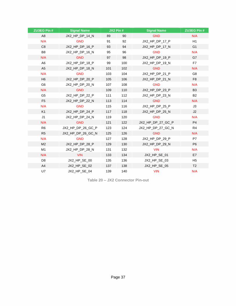
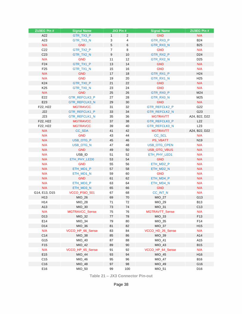
The JX1, JX2, and JX3 detail pinouts are shown in the following tables. In the following 3 tables:
– Pins in Red are Power, Ground, or Sense signals.
– Pins in Blue are dedicated signals.
– Pins in Black are multi-function/general-purpose pins.
– Pins in Black with _GC designators are multi-function/general-purpose pins or Global Clock inputs.
– HP_DP stands for High Performance Differential Pairs, HP_SE stands for High Performance Single-Ended, and HD_SE stands for High Density Single-Ended
ZU3EG Pin # Signal Name Notes Signal Name ZU3EG Pin #
K16 JTAG_TCK 1 2 JTAG_TMS L18
L17 JTAG_TDO 3 4 JTAG_TDI L15
L6, P5, U4 VCCO_HP_65 5 6 VCCO_HP_64 AA6, AB9, V7
L6, P5, U4 VCCO_HP_65 7 8 JX1_HP_DP_01_P Y7
AB8 JX1_HP_DP_00_P 9 10 JX1_HP_DP_01_N AA7
AB7 JX1_HP_DP_00_N 11 12 VCCO_HP_64 AA6, AB9, V7
L6, P5, U4 VCCO_HP_65 13 14 JX1_HP_DP_03_P AC9
AA9 JX1_HP_DP_02_P 15 16 JX1_HP_DP_03_N AC8
AA8 JX1_HP_DP_02_N 17 18 VCCO_HP_64 AA6, AB9, V7
N/A GND 19 20 JX1_HP_DP_05_P AD9
AD6 JX1_HP_DP_04_P 21 22 JX1_HP_DP_05_N AE9
AD5 JX1_HP_DP_04_N 23 24 GND N/A
N/A GND 25 26 JX1_HP_DP_07_P AD8
AE7 JX1_HP_DP_06_P 27 28 JX1_HP_DP_07_N AD7
AE6 JX1_HP_DP_06_N 29 30 GND N/A
N/A GND 31 32 JX1_HP_DP_09_P W1
AA4 JX1_HP_DP_08_P 33 34 JX1_HP_DP_09_N Y1
AA3 JX1_HP_DP_08_N 35 36 GND N/A
N/A GND 37 38 JX1_HP_DP_11_P AB2
W4 JX1_HP_DP_10_P 39 40 JX1_HP_DP_11_N AB1
Y4 JX1_HP_DP_10_N 41 42 GND N/A
N/A GND 43 44 JX1_HP_DP_13_P AB6
W3 JX1_HP_DP_12_P 45 46 JX1_HP_DP_13_N AC6
W2 JX1_HP_DP_12_N 47 48 GND N/A
N/A GND 49 50 JX1_HP_DP_15_P AE4
Y2 JX1_HP_DP_14_P 51 52 JX1_HP_DP_15_N AE3
AA2 JX1_HP_DP_14_N 53 54 GND N/A
N/A GND 55 56 JX1_HP_DP_17_P AD4
AD1 JX1_HP_DP_16_P 57 58 JX1_HP_DP_17_N AD3
AE1 JX1_HP_DP_16_N 59 60 GND N/A
N/A GND 61 62 JX1_HP_DP_19_GC_P AB3
AB5 JX1_HP_DP_18_GC_P 63 64 JX1_HP_DP_19_GC_N AC3
AC4 JX1_HP_DP_18_GC_N 65 66 GND N/A
N/A GND 67 68 JX1_HP_DP_21_GC_P Y5
W6 JX1_HP_DP_20_GC_P 69 70 JX1_HP_DP_21_GC_N AA5
Y6 JX1_HP_DP_20_GC_N 71 72 GND N/A
Page 35
ZU3EG Pin # Signal Name Notes Signal Name ZU3EG Pin #
N/A GND 73 74 JX1_HP_DP_23_P W8
AD2 JX1_HP_DP_22_P 75 76 JX1_HP_DP_23_N W7
AE2 JX1_HP_DP_22_N 77 78 GND N/A
N/A GND 79 80 JX1_HP_DP_25_P R7
T5 JX1_HP_DP_24_P 81 82 JX1_HP_DP_25_N T7
T4 JX1_HP_DP_24_N 83 84 GND N/A
N/A GND 85 86 JX1_HP_DP_27_P T3
U6 JX1_HP_DP_26_P 87 88 JX1_HP_DP_27_N U2
U5 JX1_HP_DP_26_N 89 90 GND N/A
N/A GND 91 92 JX1_HP_DP_29_P U3
P3 JX1_HP_DP_28_P 93 94 JX1_HP_DP_29_N V3
P2 JX1_HP_DP_28_N 95 96 GND N/A
N/A GND 97 98 JX1_HP_DP_31_P U1
N1 JX1_HP_DP_30_P 99 100 JX1_HP_DP_31_N V1
P1 JX1_HP_DP_30_N 101 102 GND N/A
N/A GND 103 104 JX1_HP_DP_33_P K4
J7 JX1_HP_DP_32_P 105 106 JX1_HP_DP_33_N J4
J6 JX1_HP_DP_32_N 107 108 GND N/A
N/A GND 109 110 JX1_HP_DP_35_P K6
L7 JX1_HP_DP_34_P 111 112 JX1_HP_DP_35_N K5
K7 JX1_HP_DP_34_N 113 114 GND N/A
N/A GND 115 116 JX1_HP_DP_37_GC_P M3
N4 JX1_HP_DP_36_GC_P 117 118 JX1_HP_DP_37_GC_N L3
N3 JX1_HP_DP_36_GC_N 119 120 GND N/A
N/A GND 121 122 JX1_HP_DP_39_P R2
N5 JX1_HP_DP_38_P 123 124 JX1_HP_DP_39_N R1
M5 JX1_HP_DP_38_N 125 126 GND N/A
N/A GND 127 128 JX1_HP_DP_41_P L2
M6 JX1_HP_DP_40_P 129 130 JX1_HP_DP_41_N K2
L5 JX1_HP_DP_40_N 131 132 VIN N/A
N/A VIN 133 134 JX1_HP_SE_01 AC1
V4 JX1_HP_SE_00 135 136 JX1_HP_SE_03 AC5
V5 JX1_HP_SE_02 137 138 JX1_HP_SE_05 L4
M7 JX1_HP_SE_04 139 140 VIN N/A
Table 19 – JX1 Connector Pin-out
Page 36
ZU3EG Pin # Signal Name JX2 Pin # Signal Name ZU3EG Pin #
P12 SYSMON_V_N 1 2 SYSMON_DX_N R12
N13 SYSMON_V_P 3 4 SYSMON_DX_P R13
N/A GND 5 6 GND N/A
H10 JX2_HD_SE_00_P 7 8 JX2_HD_SE_01_P C10
H9 JX2_HD_SE_00_N 9 10 JX2_HD_SE_01_N B10
N/A PMBus_SDA 11 12 PMBus_SCL N/A
B11 JX2_HD_SE_02_P 13 14 JX2_HD_SE_03_P B12
A10 JX2_HD_SE_02_N 15 16 JX2_HD_SE_03_N A12
D5, E8, G4 VCCO_HP_66 17 18 VCCO_HD_26 D10, F11
E11 JX2_HD_SE_04_GC_P 19 20 JX2_HD_SE_05_GC_P F9
E10 JX2_HD_SE_04_GC_N 21 22 JX2_HD_SE_05_GC_N E9
D5, E8, G4 VCCO_HP_66 23 24 VCCO_HD_26 D10, F11
D9 JX2_HD_SE_06_GC_P 25 26 JX2_HD_SE_07_GC_P D11
C9 JX2_HD_SE_06_GC_N 27 28 JX2_HD_SE_07_GC_N C11
D5, E8, G4 VCCO_HP_66 29 30 VCCO_HD_26 D10, F11
E12 JX2_HD_SE_08_P 31 32 JX2_HD_SE_09_P G12
D12 JX2_HD_SE_08_N 33 34 JX2_HD_SE_09_N F12
N/A PMBus_ALERT_N 35 36 CC_RESET_OUT_N N/A
H11 JX2_HD_SE_10_P 37 38 JX2_HD_SE_11_P G10
G11 JX2_HD_SE_10_N 39 40 JX2_HD_SE_11_N F10
N/A SOM_PG_OUT 41 42 SOM_RESET_IN_N N/A
N/A GND 43 44 JX2_HP_DP_01_P A3
D2 JX2_HP_DP_00_P 45 46 JX2_HP_DP_01_N A2
D1 JX2_HP_DP_00_N 47 48 GND N/A
N/A GND 49 50 JX2_HP_DP_03_P H4
C1 JX2_HP_DP_02_P 51 52 JX2_HP_DP_03_N H3
B1 JX2_HP_DP_02_N 53 54 GND N/A
N/A GND 55 56 JX2_HP_DP_05_P G3
G2 JX2_HP_DP_04_P 57 58 JX2_HP_DP_05_N F3
F2 JX2_HP_DP_04_N 59 60 GND N/A
N/A GND 61 62 JX2_HP_DP_07_P F4
E2 JX2_HP_DP_06_P 63 64 JX2_HP_DP_07_N E4
E1 JX2_HP_DP_06_N 65 66 GND N/A
N/A GND 67 68 JX2_HP_DP_09_P C6
B7 JX2_HP_DP_08_P 69 70 JX2_HP_DP_09_N B6
A7 JX2_HP_DP_08_N 71 72 GND N/A
N/A GND 73 74 JX2_HP_DP_11_GC_P E6
D7 JX2_HP_DP_10_GC_P 75 76 JX2_HP_DP_11_GC_N E5
D6 JX2_HP_DP_10_GC_N 77 78 GND N/A
N/A GND 79 80 JX2_HP_DP_13_GC_P D4
C4 JX2_HP_DP_12_GC_P 81 82 JX2_HP_DP_13_GC_N D3
C3 JX2_HP_DP_12_GC_N 83 84 GND N/A
N/A GND 85 86 JX2_HP_DP_15_P C5
A9 JX2_HP_DP_14_P 87 88 JX2_HP_DP_15_N B5
Page 37
ZU3EG Pin # Signal Name JX2 Pin # Signal Name ZU3EG Pin #
A8 JX2_HP_DP_14_N 89 90 GND N/A
N/A GND 91 92 JX2_HP_DP_17_P H1
C8 JX2_HP_DP_16_P 93 94 JX2_HP_DP_17_N G1
B8 JX2_HP_DP_16_N 95 96 GND N/A
N/A GND 97 98 JX2_HP_DP_19_P G7
A6 JX2_HP_DP_18_P 99 100 JX2_HP_DP_19_N F7
A5 JX2_HP_DP_18_N 101 102 GND N/A
N/A GND 103 104 JX2_HP_DP_21_P G8
H6 JX2_HP_DP_20_P 105 106 JX2_HP_DP_21_N F8
G6 JX2_HP_DP_20_N 107 108 GND N/A
N/A GND 109 110 JX2_HP_DP_23_P B3
G5 JX2_HP_DP_22_P 111 112 JX2_HP_DP_23_N B2
F5 JX2_HP_DP_22_N 113 114 GND N/A
N/A GND 115 116 JX2_HP_DP_25_P J3
K1 JX2_HP_DP_24_P 117 118 JX2_HP_DP_25_N J2
J1 JX2_HP_DP_24_N 119 120 GND N/A
N/A GND 121 122 JX2_HP_DP_27_GC_P P4
R6 JX2_HP_DP_26_GC_P 123 124 JX2_HP_DP_27_GC_N R4
R5 JX2_HP_DP_26_GC_N 125 126 GND N/A
N/A GND 127 128 JX2_HP_DP_29_P P7
M2 JX2_HP_DP_28_P 129 130 JX2_HP_DP_29_N P6
M1 JX2_HP_DP_28_N 131 132 VIN N/A
N/A VIN 133 134 JX2_HP_SE_01 E7
D8 JX2_HP_SE_00 135 136 JX2_HP_SE_03 H5
A4 JX2_HP_SE_02 137 138 JX2_HP_SE_05 T2
U7 JX2_HP_SE_04 139 140 VIN N/A
Table 20 – JX2 Connector Pin-out
Page 38
ZU3EG Pin # Signal Name JX3 Pin # Signal Name ZU3EG Pin #
A22 GTR_TX3_P 1 2 GND N/A
A23 GTR_TX3_N 3 4 GTR_RX3_P B24
N/A GND 5 6 GTR_RX3_N B25
C22 GTR_TX2_P 7 8 GND N/A
C23 GTR_TX2_N 9 10 GTR_RX2_P D24
N/A GND 11 12 GTR_RX2_N D25
F24 GTR_TX1_P 13 14 GND N/A
F25 GTR_TX1_N 15 16 GND N/A
N/A GND 17 18 GTR_RX1_P H24
N/A GND 19 20 GTR_RX1_N H25
K24 GTR_TX0_P 21 22 GND N/A
K25 GTR_TX0_N 23 24 GND N/A
N/A GND 25 26 GTR_RX0_P M24
E22 GTR_REFCLK3_P 27 28 GTR_RX0_N M25
E23 GTR_REFCLK3_N 29 30 GND N/A
F22, H22 MGTRAVCC 31 32 GTR_REFCLK2_P G22
J22 GTR_REFCLK1_P 33 34 GTR_REFCLK2_N G23
J23 GTR_REFCLK1_N 35 36 MGTRAVTT A24, B22, D22
F22, H22 MGTRAVCC 37 38 GTR_REFCLK0_P L22
F22, H22 MGTRAVCC 39 40 GTR_REFCLK0_N L23
N/A CC_SDA 41 42 MGTRAVTT A24, B22, D22
N/A GND 43 44 CC_SCL N/A
N/A USB_OTG_P 45 46 PS_VBATT N19
N/A USB_OTG_N 47 48 USB_OTG_CPEN N/A
N/A GND 49 50 USB_OTG_VBUS N/A
N/A USB_ID 51 52 ETH_PHY_LED1 N/A
N/A ETH_PHY_LED0 53 54 GND N/A
N/A GND 55 56 ETH_MD2_P N/A
N/A ETH_MD1_P 57 58 ETH_MD2_N N/A
N/A ETH_MD1_N 59 60 GND N/A
N/A GND 61 62 ETH_MD4_P N/A
N/A ETH_MD3_P 63 64 ETH_MD4_N N/A
N/A ETH_MD3_N 65 66 GND N/A
G14, E13, D15 VCCO_PSIO_501 67 68 CC_INT_N N/A
H13 MIO_26 69 70 MIO_27 G13
H14 MIO_28 71 72 MIO_29 B13
A13 MIO_30 73 74 MIO_31 C13
N/A MGTRAVCC_Sense 75 76 MGTRAVTT_Sense N/A
D13 MIO_32 77 78 MIO_33 F13
E14 MIO_34 79 80 MIO_35 F14
D14 MIO_36 81 82 MIO_37 H15
N/A VCCO_HP_66_Sense 83 84 VCCO_HD_26_Sense N/A
C14 MIO_38 85 86 MIO_39 A14
G15 MIO_40 87 88 MIO_41 A15
F15 MIO_42 89 90 MIO_43 B15
N/A VCCO_HP_65_Sense 91 92 VCCO_HP_64_Sense N/A
E15 MIO_44 93 94 MIO_45 H16
C15 MIO_46 95 96 MIO_47 B16
C16 MIO_48 97 98 MIO_49 G16
E16 MIO_50 99 100 MIO_51 D16
Table 21 – JX3 Connector Pin-out
Page 39
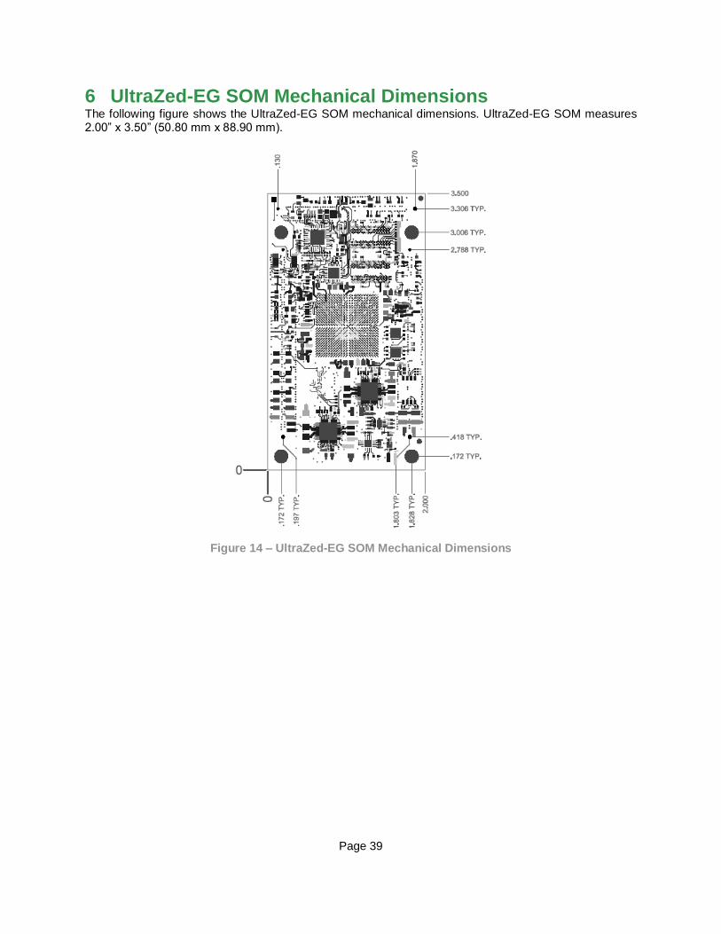
6 UltraZed-EG SOM Mechanical Dimensions The following figure shows the UltraZed-EG SOM mechanical dimensions. UltraZed-EG SOM measures 2.00” x 3.50” (50.80 mm x 88.90 mm).
Figure 14 – UltraZed-EG SOM Mechanical Dimensions
Page 40
7 Carrier Card PCB Design Guidelines The following sections provide general PCB design guidelines for designing with the UltraZed-EG SOM. PCB design files for the Avnet UltraZed Carrier Cards are available upon request to assist you with your custom Carrier Card PCB design.
7.1 Connector Land and Alignment It is extremely important that Carrier card designers ensure that the Micro Headers have the proper land patterns and that the connectors are aligned correctly. The land pattern is featured in the Mechanical Considerations section of this document. Connector alignment is ensured if the alignment pin holes in the PCB connector pattern are in the correct positions and if the holes are drilled to the proper size and tolerance by the PCB fabricator.
Please refer to the UltraZed-EG SOM mechanical drawing available on the UltraZed-EG SOM documentation page www.ultrazed.org/product/ultrazed-EG for more information.
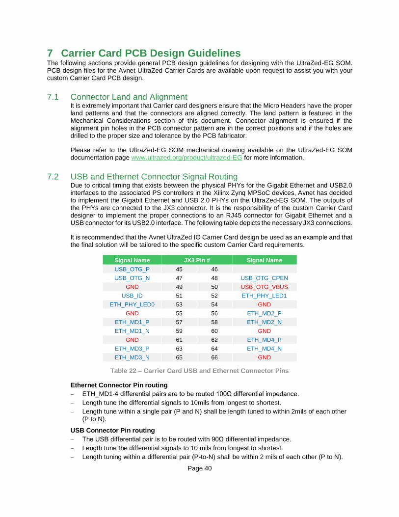
7.2 USB and Ethernet Connector Signal Routing Due to critical timing that exists between the physical PHYs for the Gigabit Ethernet and USB2.0 interfaces to the associated PS controllers in the Xilinx Zynq MPSoC devices, Avnet has decided to implement the Gigabit Ethernet and USB 2.0 PHYs on the UltraZed-EG SOM. The outputs of the PHYs are connected to the JX3 connector. It is the responsibility of the custom Carrier Card designer to implement the proper connections to an RJ45 connector for Gigabit Ethernet and a USB connector for its USB2.0 interface. The following table depicts the necessary JX3 connections.
It is recommended that the Avnet UltraZed IO Carrier Card design be used as an example and that the final solution will be tailored to the specific custom Carrier Card requirements.
Signal Name JX3 Pin # Signal Name
USB_OTG_P 45 46
USB_OTG_N 47 48 USB_OTG_CPEN
GND 49 50 USB_OTG_VBUS
USB_ID 51 52 ETH_PHY_LED1
ETH_PHY_LED0 53 54 GND
GND 55 56 ETH_MD2_P
ETH_MD1_P 57 58 ETH_MD2_N
ETH_MD1_N 59 60 GND
GND 61 62 ETH_MD4_P
ETH_MD3_P 63 64 ETH_MD4_N
ETH_MD3_N 65 66 GND
Table 22 – Carrier Card USB and Ethernet Connector Pins
Ethernet Connector Pin routing
– ETH_MD1-4 differential pairs are to be routed 100Ω differential impedance.
– Length tune the differential signals to 10mils from longest to shortest.
– Length tune within a single pair (P and N) shall be length tuned to within 2mils of each other (P to N).
USB Connector Pin routing
– The USB differential pair is to be routed with 90Ω differential impedance.
– Length tune the differential signals to 10 mils from longest to shortest.
– Length tuning within a differential pair (P-to-N) shall be within 2 mils of each other (P to N).
Page 41
7.3 PS GTR Transceiver Signal Routing It is highly recommended that the guidelines described in the Xilinx document “UltraScale Architecture PCB Design” (UG583), be reviewed prior to designing and routing GTR circuits. Here are some general guidelines that are followed on the UltraZed-EG SOM’s GTR routing:
– All gigabit transceiver signals shall be routed as striplines.
– All Multi-Gigabit Transceiver TX, RX and related clock differential signals shall be routed differential at 100Ω differential impedance.
– Use 4x spacing between pairs.
– All Multi-Gigabit Transceiver differential signals can be treated as a group and shall be length tuned to within 10mils from the shortest pair to longest pair.
– All Multi-Gigabit Transceiver signals within a single pair (P and N) shall be length tuned to within 2 mils of each other (P to N).
– No More than two transitions (vias) are allowed for these signals.
– Multi-Gigabit Transceiver reference clocks do not need to be length tuned to the data signal pairs, but should be length tuned to each other within 10mils from the shortest pair to the longest pair.
– Multi-Gigabit Transceiver reference clock pairs must be tuned to within 2 mils (P to N).
The GTR transceiver routing on the Avnet IO Carrier Card should be used as reference for routing the GTRs on a custom Carrier Card. Please refer to the IO Carrier Card PCB Layout Files on the www.ultrazed.org/product/ultrazed-io-carrier-card website for more information. User should also use Signal Integrity (SI) analysis prior to fabricating the custom Carrier Card PCB. Avnet used Fidus SI analysis services (www.fidus.com) to achieve the desired GTR performance on the Avnet IO Carrier Card.
7.4 PS MIO Routing The routing of the PS MIO signals on the custom Carrier Cards depends on how these signals are defined and used. The PS MIO pins can be used to implement the following interfaces on the custom Carrier Cards:
– SD/microSD Card
– UART
– SPI
– I2C
– GPIO
– CAN
When routing the PS MIO signals, they should be length matched within each interface type. The following states general guidelines for routing the PS MIO signals on the custom Carrier Card.
– All signals are to be routed 50Ω characteristic impedance.
7.5 PL SYSMON Signal Routing The PL SYSMON interface is connected to the bank 0 of the Zynq UltraScale+ MPSoC and consists of VP, VN, DXP, and DXN pins. These pins are routed to the JX2 connector and can be used on custom Carrier Cards to implement low speed analog interface. The SYSMON supply voltages, VCCADC and VREF are provided on the UltraZed-EG SOM. Here are some general guidelines for designing the SYSMON interface on the custom Carrier Cards.
– Use 4X spacing on the traces.
– Single ended impedance is 50Ω and differential is 100Ω.
– All paired signals should be routed to within 50mils of each other.
– All interface signals should be routed to within 100mils of each other.
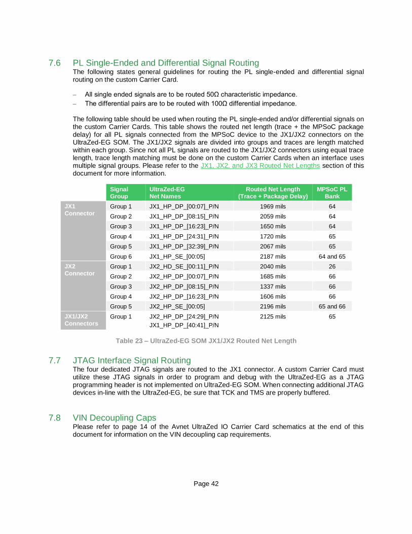
Page 42
7.6 PL Single-Ended and Differential Signal Routing The following states general guidelines for routing the PL single-ended and differential signal routing on the custom Carrier Card.
– All single ended signals are to be routed 50Ω characteristic impedance.
– The differential pairs are to be routed with 100Ω differential impedance.
The following table should be used when routing the PL single-ended and/or differential signals on the custom Carrier Cards. This table shows the routed net length (trace + the MPSoC package delay) for all PL signals connected from the MPSoC device to the JX1/JX2 connectors on the UltraZed-EG SOM. The JX1/JX2 signals are divided into groups and traces are length matched within each group. Since not all PL signals are routed to the JX1/JX2 connectors using equal trace length, trace length matching must be done on the custom Carrier Cards when an interface uses multiple signal groups. Please refer to the JX1, JX2, and JX3 Routed Net Lengths section of this document for more information.
Signal Group
UltraZed-EG Net Names
Routed Net Length (Trace + Package Delay)
MPSoC PL Bank
JX1 Connector
Group 1 JX1_HP_DP_[00:07]_P/N 1969 mils 64
Group 2 JX1_HP_DP_[08:15]_P/N 2059 mils 64
Group 3 JX1_HP_DP_[16:23]_P/N 1650 mils 64
Group 4 JX1_HP_DP_[24:31]_P/N 1720 mils 65
Group 5 JX1_HP_DP_[32:39]_P/N 2067 mils 65
Group 6 JX1_HP_SE_[00:05] 2187 mils 64 and 65
JX2 Connector
Group 1 JX2_HD_SE_[00:11]_P/N 2040 mils 26
Group 2 JX2_HP_DP_[00:07]_P/N 1685 mils 66
Group 3 JX2_HP_DP_[08:15]_P/N 1337 mils 66
Group 4 JX2_HP_DP_[16:23]_P/N 1606 mils 66
Group 5 JX2_HP_SE_[00:05] 2196 mils 65 and 66
JX1/JX2 Connectors
Group 1 JX2_HP_DP_[24:29]_P/N
JX1_HP_DP_[40:41]_P/N
2125 mils 65
Table 23 – UltraZed-EG SOM JX1/JX2 Routed Net Length
7.7 JTAG Interface Signal Routing The four dedicated JTAG signals are routed to the JX1 connector. A custom Carrier Card must utilize these JTAG signals in order to program and debug with the UltraZed-EG as a JTAG programming header is not implemented on UltraZed-EG SOM. When connecting additional JTAG devices in-line with the UltraZed-EG, be sure that TCK and TMS are properly buffered.
7.8 VIN Decoupling Caps Please refer to page 14 of the Avnet UltraZed IO Carrier Card schematics at the end of this document for information on the VIN decoupling cap requirements.
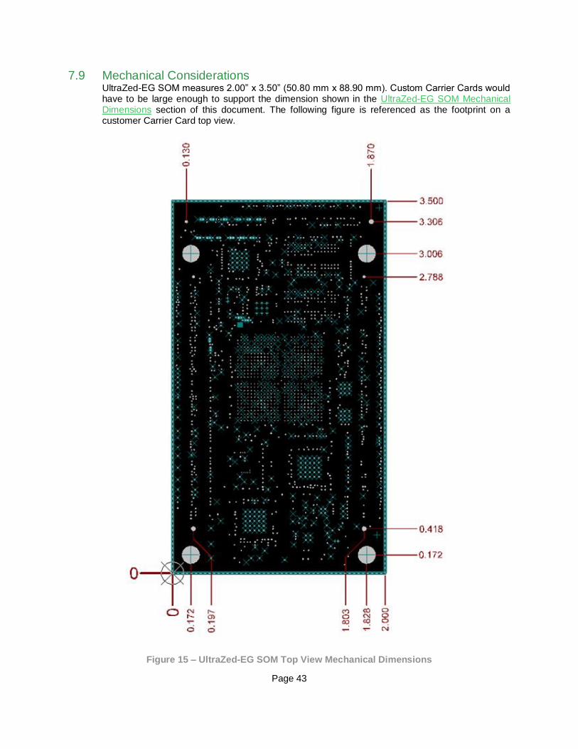
Page 43
7.9 Mechanical Considerations UltraZed-EG SOM measures 2.00” x 3.50” (50.80 mm x 88.90 mm). Custom Carrier Cards would have to be large enough to support the dimension shown in the UltraZed-EG SOM Mechanical Dimensions section of this document. The following figure is referenced as the footprint on a customer Carrier Card top view.
Figure 15 – UltraZed-EG SOM Top View Mechanical Dimensions
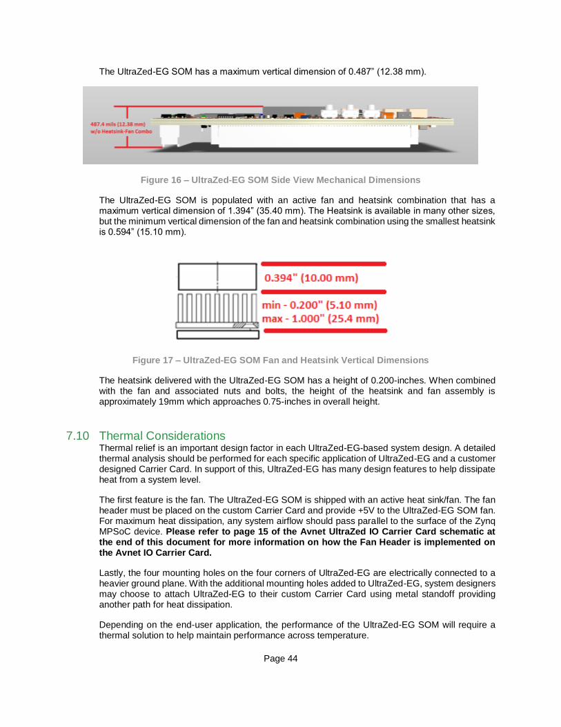
Page 44
The UltraZed-EG SOM has a maximum vertical dimension of 0.487” (12.38 mm).
Figure 16 – UltraZed-EG SOM Side View Mechanical Dimensions
The UltraZed-EG SOM is populated with an active fan and heatsink combination that has a maximum vertical dimension of 1.394” (35.40 mm). The Heatsink is available in many other sizes, but the minimum vertical dimension of the fan and heatsink combination using the smallest heatsink is 0.594” (15.10 mm).
Figure 17 – UltraZed-EG SOM Fan and Heatsink Vertical Dimensions
The heatsink delivered with the UltraZed-EG SOM has a height of 0.200-inches. When combined with the fan and associated nuts and bolts, the height of the heatsink and fan assembly is approximately 19mm which approaches 0.75-inches in overall height.
7.10 Thermal Considerations Thermal relief is an important design factor in each UltraZed-EG-based system design. A detailed thermal analysis should be performed for each specific application of UltraZed-EG and a customer designed Carrier Card. In support of this, UltraZed-EG has many design features to help dissipate heat from a system level.
The first feature is the fan. The UltraZed-EG SOM is shipped with an active heat sink/fan. The fan header must be placed on the custom Carrier Card and provide +5V to the UltraZed-EG SOM fan. For maximum heat dissipation, any system airflow should pass parallel to the surface of the Zynq MPSoC device. Please refer to page 15 of the Avnet UltraZed IO Carrier Card schematic at the end of this document for more information on how the Fan Header is implemented on the Avnet IO Carrier Card.
Lastly, the four mounting holes on the four corners of UltraZed-EG are electrically connected to a heavier ground plane. With the additional mounting holes added to UltraZed-EG, system designers may choose to attach UltraZed-EG to their custom Carrier Card using metal standoff providing another path for heat dissipation.
Depending on the end-user application, the performance of the UltraZed-EG SOM will require a thermal solution to help maintain performance across temperature.
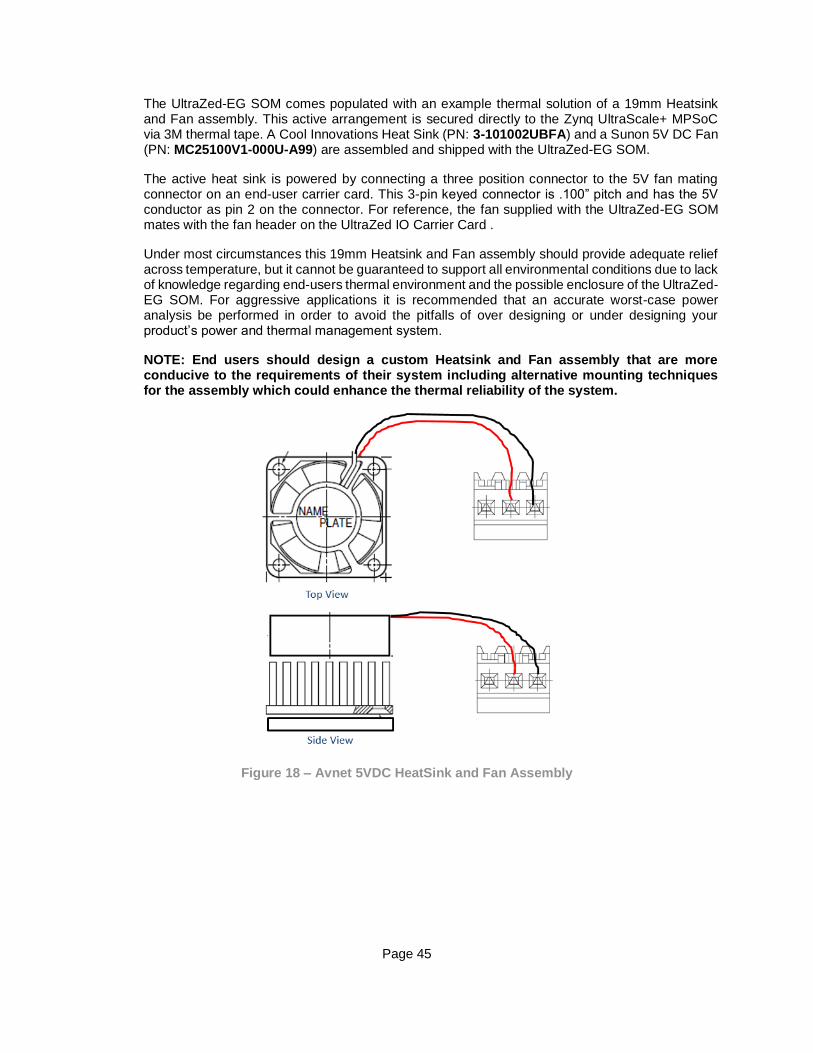
Page 45
The UltraZed-EG SOM comes populated with an example thermal solution of a 19mm Heatsink and Fan assembly. This active arrangement is secured directly to the Zynq UltraScale+ MPSoC via 3M thermal tape. A Cool Innovations Heat Sink (PN: 3-101002UBFA) and a Sunon 5V DC Fan (PN: MC25100V1-000U-A99) are assembled and shipped with the UltraZed-EG SOM.
The active heat sink is powered by connecting a three position connector to the 5V fan mating connector on an end-user carrier card. This 3-pin keyed connector is .100” pitch and has the 5V conductor as pin 2 on the connector. For reference, the fan supplied with the UltraZed-EG SOM mates with the fan header on the UltraZed IO Carrier Card .
Under most circumstances this 19mm Heatsink and Fan assembly should provide adequate relief across temperature, but it cannot be guaranteed to support all environmental conditions due to lack of knowledge regarding end-users thermal environment and the possible enclosure of the UltraZed-EG SOM. For aggressive applications it is recommended that an accurate worst-case power analysis be performed in order to avoid the pitfalls of over designing or under designing your product’s power and thermal management system.
NOTE: End users should design a custom Heatsink and Fan assembly that are more conducive to the requirements of their system including alternative mounting techniques for the assembly which could enhance the thermal reliability of the system.
Figure 18 – Avnet 5VDC HeatSink and Fan Assembly

Page 46
8 Getting Help and Support If additional support is required, Avnet has many avenues to search depending on your needs.
For general question regarding UltraZed-EG SOM and Carrier Card or accessories, please visit our website at www.ultrazed.org/product/ultrazed-EG. Here you can find documentation, technical specifications, videos and tutorials, reference designs and other support.
Detailed questions regarding UltraZed-EG SOM hardware design, software application development, using Xilinx tools, training and other topics can be posted on the UltraZed-EG Support Forums at http://www.picozed.org/forums/zed-english-forum. Avnet’s technical support team monitors the forum during normal business hours.
Those interested in customer-specific options on UltraZed-EG SOM can send inquiries to [email protected].
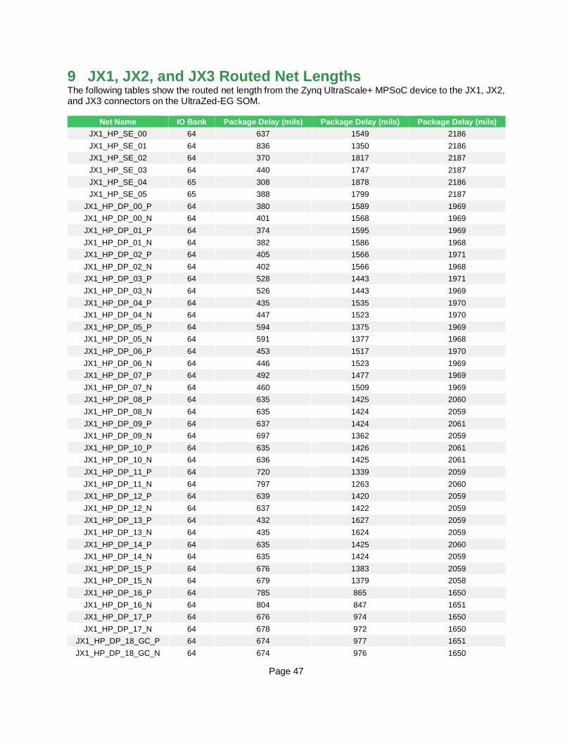
Page 47
9 JX1, JX2, and JX3 Routed Net Lengths The following tables show the routed net length from the Zynq UltraScale+ MPSoC device to the JX1, JX2, and JX3 connectors on the UltraZed-EG SOM.
Net Name IO Bank Package Delay (mils) Package Delay (mils) Package Delay (mils)
JX1_HP_SE_00 64 637 1549 2186
JX1_HP_SE_01 64 836 1350 2186
JX1_HP_SE_02 64 370 1817 2187
JX1_HP_SE_03 64 440 1747 2187
JX1_HP_SE_04 65 308 1878 2186
JX1_HP_SE_05 65 388 1799 2187
JX1_HP_DP_00_P 64 380 1589 1969
JX1_HP_DP_00_N 64 401 1568 1969
JX1_HP_DP_01_P 64 374 1595 1969
JX1_HP_DP_01_N 64 382 1586 1968
JX1_HP_DP_02_P 64 405 1566 1971
JX1_HP_DP_02_N 64 402 1566 1968
JX1_HP_DP_03_P 64 528 1443 1971
JX1_HP_DP_03_N 64 526 1443 1969
JX1_HP_DP_04_P 64 435 1535 1970
JX1_HP_DP_04_N 64 447 1523 1970
JX1_HP_DP_05_P 64 594 1375 1969
JX1_HP_DP_05_N 64 591 1377 1968
JX1_HP_DP_06_P 64 453 1517 1970
JX1_HP_DP_06_N 64 446 1523 1969
JX1_HP_DP_07_P 64 492 1477 1969
JX1_HP_DP_07_N 64 460 1509 1969
JX1_HP_DP_08_P 64 635 1425 2060
JX1_HP_DP_08_N 64 635 1424 2059
JX1_HP_DP_09_P 64 637 1424 2061
JX1_HP_DP_09_N 64 697 1362 2059
JX1_HP_DP_10_P 64 635 1426 2061
JX1_HP_DP_10_N 64 636 1425 2061
JX1_HP_DP_11_P 64 720 1339 2059
JX1_HP_DP_11_N 64 797 1263 2060
JX1_HP_DP_12_P 64 639 1420 2059
JX1_HP_DP_12_N 64 637 1422 2059
JX1_HP_DP_13_P 64 432 1627 2059
JX1_HP_DP_13_N 64 435 1624 2059
JX1_HP_DP_14_P 64 635 1425 2060
JX1_HP_DP_14_N 64 635 1424 2059
JX1_HP_DP_15_P 64 676 1383 2059
JX1_HP_DP_15_N 64 679 1379 2058
JX1_HP_DP_16_P 64 785 865 1650
JX1_HP_DP_16_N 64 804 847 1651
JX1_HP_DP_17_P 64 676 974 1650
JX1_HP_DP_17_N 64 678 972 1650
JX1_HP_DP_18_GC_P 64 674 977 1651
JX1_HP_DP_18_GC_N 64 674 976 1650
Page 48
Net Name IO Bank Package Delay (mils) Package Delay (mils) Package Delay (mils)
JX1_HP_DP_19_GC_P 64 679 971 1650
JX1_HP_DP_19_GC_N 64 676 974 1650
JX1_HP_DP_20_GC_P 64 519 1131 1650
JX1_HP_DP_20_GC_N 64 521 1129 1650
JX1_HP_DP_21_GC_P 64 518 1132 1650
JX1_HP_DP_21_GC_N 64 516 1133 1649
JX1_HP_DP_22_P 64 706 944 1650
JX1_HP_DP_22_N 64 739 910 1649
JX1_HP_DP_23_P 64 386 1264 1650
JX1_HP_DP_23_N 64 378 1272 1650
JX1_HP_DP_24_P 65 439 1282 1721
JX1_HP_DP_24_N 65 509 1213 1722
JX1_HP_DP_25_P 65 345 1377 1722
JX1_HP_DP_25_N 65 350 1372 1722
JX1_HP_DP_26_P 65 507 1213 1720
JX1_HP_DP_26_N 65 506 1215 1721
JX1_HP_DP_27_P 65 420 1301 1721
JX1_HP_DP_27_N 65 419 1303 1722
JX1_HP_DP_28_P 65 421 1298 1719
JX1_HP_DP_28_N 65 473 1249 1722
JX1_HP_DP_29_P 65 420 1303 1723
JX1_HP_DP_29_N 65 421 1300 1721
JX1_HP_DP_30_P 65 421 1300 1721
JX1_HP_DP_30_N 65 434 1288 1722
JX1_HP_DP_31_P 65 419 1302 1721
JX1_HP_DP_31_N 65 420 1301 1721
JX1_HP_DP_32_P 65 469 1598 2067
JX1_HP_DP_32_N 65 411 1655 2066
JX1_HP_DP_33_P 65 387 1683 2070
JX1_HP_DP_33_N 65 436 1634 2070
JX1_HP_DP_34_P 65 411 1657 2068
JX1_HP_DP_34_N 65 403 1664 2067
JX1_HP_DP_35_P 65 393 1676 2069
JX1_HP_DP_35_N 65 403 1665 2068
JX1_HP_DP_36_GC_P 65 412 1655 2067
JX1_HP_DP_36_GC_N 65 383 1684 2067
JX1_HP_DP_37_GC_P 65 505 1563 2068
JX1_HP_DP_37_GC_N 65 511 1556 2067
JX1_HP_DP_38_P 65 306 1761 2067
JX1_HP_DP_38_N 65 305 1762 2067
JX1_HP_DP_39_P 65 490 1575 2065
JX1_HP_DP_39_N 65 492 1575 2067
JX1_HP_DP_40_P 65 427 1698 2125
JX1_HP_DP_40_N 65 432 1693 2125
JX1_HP_DP_41_P 65 387 1737 2124
JX1_HP_DP_41_N 65 382 1743 2125
Table 24 – JX1 Connector Routed Net Length
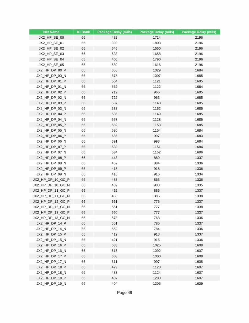
Page 49
Net Name IO Bank Package Delay (mils) Package Delay (mils) Package Delay (mils)
JX2_HP_SE_00 66 482 1714 2196
JX2_HP_SE_01 66 393 1803 2196
JX2_HP_SE_02 66 646 1550 2196
JX2_HP_SE_03 66 538 1658 2196
JX2_HP_SE_04 65 406 1790 2196
JX2_HP_SE_05 65 580 1616 2196
JX2_HP_DP_00_P 66 655 1029 1684
JX2_HP_DP_00_N 66 678 1007 1685
JX2_HP_DP_01_P 66 564 1121 1685
JX2_HP_DP_01_N 66 562 1122 1684
JX2_HP_DP_02_P 66 719 966 1685
JX2_HP_DP_02_N 66 722 963 1685
JX2_HP_DP_03_P 66 537 1148 1685
JX2_HP_DP_03_N 66 533 1152 1685
JX2_HP_DP_04_P 66 536 1149 1685
JX2_HP_DP_04_N 66 557 1128 1685
JX2_HP_DP_05_P 66 532 1153 1685
JX2_HP_DP_05_N 66 530 1154 1684
JX2_HP_DP_06_P 66 686 997 1683
JX2_HP_DP_06_N 66 691 993 1684
JX2_HP_DP_07_P 66 533 1151 1684
JX2_HP_DP_07_N 66 534 1152 1686
JX2_HP_DP_08_P 66 448 889 1337
JX2_HP_DP_08_N 66 452 884 1336
JX2_HP_DP_09_P 66 418 918 1336
JX2_HP_DP_09_N 66 418 916 1334
JX2_HP_DP_10_GC_P 66 483 853 1336
JX2_HP_DP_10_GC_N 66 432 903 1335
JX2_HP_DP_11_GC_P 66 452 885 1337
JX2_HP_DP_11_GC_N 66 453 885 1338
JX2_HP_DP_12_GC_P 66 561 776 1337
JX2_HP_DP_12_GC_N 66 561 777 1338
JX2_HP_DP_13_GC_P 66 560 777 1337
JX2_HP_DP_13_GC_N 66 573 763 1336
JX2_HP_DP_14_P 66 551 786 1337
JX2_HP_DP_14_N 66 552 784 1336
JX2_HP_DP_15_P 66 419 918 1337
JX2_HP_DP_15_N 66 421 915 1336
JX2_HP_DP_16_P 66 583 1025 1608
JX2_HP_DP_16_N 66 515 1092 1607
JX2_HP_DP_17_P 66 608 1000 1608
JX2_HP_DP_17_N 66 611 997 1608
JX2_HP_DP_18_P 66 479 1128 1607
JX2_HP_DP_18_N 66 483 1124 1607
JX2_HP_DP_19_P 66 407 1200 1607
JX2_HP_DP_19_N 66 404 1205 1609
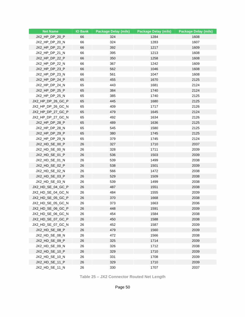
Page 50
Net Name IO Bank Package Delay (mils) Package Delay (mils) Package Delay (mils)
JX2_HP_DP_20_P 66 324 1284 1608
JX2_HP_DP_20_N 66 324 1283 1607
JX2_HP_DP_21_P 66 392 1217 1609
JX2_HP_DP_21_N 66 395 1213 1608
JX2_HP_DP_22_P 66 350 1258 1608
JX2_HP_DP_22_N 66 367 1242 1609
JX2_HP_DP_23_P 66 562 1046 1608
JX2_HP_DP_23_N 66 561 1047 1608
JX2_HP_DP_24_P 65 455 1670 2125
JX2_HP_DP_24_N 65 443 1681 2124
JX2_HP_DP_25_P 65 384 1740 2124
JX2_HP_DP_25_N 65 385 1740 2125
JX2_HP_DP_26_GC_P 65 445 1680 2125
JX2_HP_DP_26_GC_N 65 409 1717 2126
JX2_HP_DP_27_GC_P 65 479 1645 2124
JX2_HP_DP_27_GC_N 65 492 1634 2126
JX2_HP_DP_28_P 65 489 1636 2125
JX2_HP_DP_28_N 65 545 1580 2125
JX2_HP_DP_29_P 65 380 1745 2125
JX2_HP_DP_29_N 65 379 1745 2124
JX2_HD_SE_00_P 26 327 1710 2037
JX2_HD_SE_00_N 26 328 1711 2039
JX2_HD_SE_01_P 26 536 1503 2039
JX2_HD_SE_01_N 26 539 1499 2038
JX2_HD_SE_02_P 26 538 1501 2039
JX2_HD_SE_02_N 26 566 1472 2038
JX2_HD_SE_03_P 26 529 1509 2038
JX2_HD_SE_03_N 26 539 1499 2038
JX2_HD_SE_04_GC_P 26 487 1551 2038
JX2_HD_SE_04_GC_N 26 484 1555 2039
JX2_HD_SE_05_GC_P 26 370 1668 2038
JX2_HD_SE_05_GC_N 26 373 1663 2036
JX2_HD_SE_06_GC_P 26 448 1591 2039
JX2_HD_SE_06_GC_N 26 454 1584 2038
JX2_HD_SE_07_GC_P 26 450 1588 2038
JX2_HD_SE_07_GC_N 26 452 1587 2039
JX2_HD_SE_08_P 26 479 1560 2039
JX2_HD_SE_08_N 26 472 1566 2038
JX2_HD_SE_09_P 26 325 1714 2039
JX2_HD_SE_09_N 26 326 1712 2038
JX2_HD_SE_10_P 26 329 1710 2039
JX2_HD_SE_10_N 26 331 1708 2039
JX2_HD_SE_11_P 26 329 1710 2039
JX2_HD_SE_11_N 26 330 1707 2037
Table 25 – JX2 Connector Routed Net Length
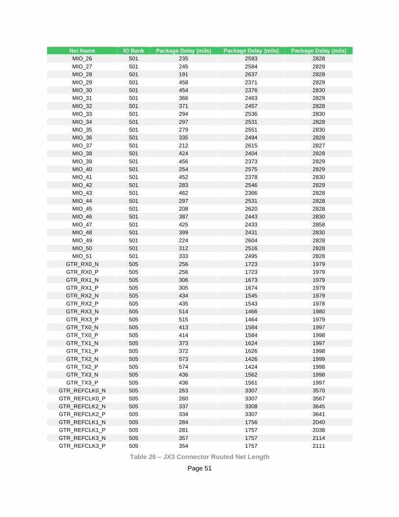
Page 51
Net Name IO Bank Package Delay (mils) Package Delay (mils) Package Delay (mils)
MIO_26 501 235 2593 2828
MIO_27 501 245 2584 2829
MIO_28 501 191 2637 2828
MIO_29 501 458 2371 2829
MIO_30 501 454 2376 2830
MIO_31 501 366 2463 2829
MIO_32 501 371 2457 2828
MIO_33 501 294 2536 2830
MIO_34 501 297 2531 2828
MIO_35 501 279 2551 2830
MIO_36 501 335 2494 2829
MIO_37 501 212 2615 2827
MIO_38 501 424 2404 2828
MIO_39 501 456 2373 2829
MIO_40 501 254 2575 2829
MIO_41 501 452 2378 2830
MIO_42 501 283 2546 2829
MIO_43 501 462 2366 2828
MIO_44 501 297 2531 2828
MIO_45 501 208 2620 2828
MIO_46 501 387 2443 2830
MIO_47 501 425 2433 2858
MIO_48 501 399 2431 2830
MIO_49 501 224 2604 2828
MIO_50 501 312 2516 2828
MIO_51 501 333 2495 2828
GTR_RX0_N 505 256 1723 1979
GTR_RX0_P 505 256 1723 1979
GTR_RX1_N 505 306 1673 1979
GTR_RX1_P 505 305 1674 1979
GTR_RX2_N 505 434 1545 1979
GTR_RX2_P 505 435 1543 1978
GTR_RX3_N 505 514 1466 1980
GTR_RX3_P 505 515 1464 1979
GTR_TX0_N 505 413 1584 1997
GTR_TX0_P 505 414 1584 1998
GTR_TX1_N 505 373 1624 1997
GTR_TX1_P 505 372 1626 1998
GTR_TX2_N 505 573 1426 1999
GTR_TX2_P 505 574 1424 1998
GTR_TX3_N 505 436 1562 1998
GTR_TX3_P 505 436 1561 1997
GTR_REFCLK0_N 505 263 3307 3570
GTR_REFCLK0_P 505 260 3307 3567
GTR_REFCLK2_N 505 337 3308 3645
GTR_REFCLK2_P 505 334 3307 3641
GTR_REFCLK1_N 505 284 1756 2040
GTR_REFCLK1_P 505 281 1757 2038
GTR_REFCLK3_N 505 357 1757 2114
GTR_REFCLK3_P 505 354 1757 2111
Table 26 – JX3 Connector Routed Net Length
Page 52
10 UltraZed-EG SOM Schematics The following pages show the Avnet UltraZed-EG SOM schematics.
Page 53
11 Avnet UltraZed IO Carrier Card Schematics The following pages show the Avnet UltraZed IO Carrier Card schematics to be used as reference when designing custom Carrier Cards.