Embed Size (px)
Citation preview

1
AVC Logic FamilyTechnology and Applications
SCEA006AAugust 1998

2
IMPORTANT NOTICE
Texas Instruments and its subsidiaries (TI) reserve the right to make changes to their productsor to discontinue any product or service without notice, and advise customers to obtain the latestversion of relevant information to verify, before placing orders, that information being relied onis current and complete. All products are sold subject to the terms and conditions of sale suppliedat the time of order acknowledgement, including those pertaining to warranty, patentinfringement, and limitation of liability.
TI warrants performance of its semiconductor products to the specifications applicable at thetime of sale in accordance with TI’s standard warranty. Testing and other quality controltechniques are utilized to the extent TI deems necessary to support this warranty. Specific testingof all parameters of each device is not necessarily performed, except those mandated bygovernment requirements.
CERTAIN APPLICATIONS USING SEMICONDUCTOR PRODUCTS MAY INVOLVEPOTENTIAL RISKS OF DEATH, PERSONAL INJURY, OR SEVERE PROPERTY ORENVIRONMENTAL DAMAGE (“CRITICAL APPLICATIONS”). TI SEMICONDUCTORPRODUCTS ARE NOT DESIGNED, AUTHORIZED, OR WARRANTED TO BE SUITABLE FORUSE IN LIFE-SUPPORT DEVICES OR SYSTEMS OR OTHER CRITICAL APPLICATIONS.INCLUSION OF TI PRODUCTS IN SUCH APPLICATIONS IS UNDERSTOOD TO BE FULLYAT THE CUSTOMER’S RISK.
In order to minimize risks associated with the customer’s applications, adequate design andoperating safeguards must be provided by the customer to minimize inherent or proceduralhazards.
TI assumes no liability for applications assistance or customer product design. TI does notwarrant or represent that any license, either express or implied, is granted under any patent right,copyright, mask work right, or other intellectual property right of TI covering or relating to anycombination, machine, or process in which such semiconductor products or services might beor are used. TI’s publication of information regarding any third party’s products or services doesnot constitute TI’s approval, warranty or endorsement thereof.
Copyright 1998, Texas Instruments Incorporated

iii
ContentsTitle Page
Abstract 1. . . . . . . . . . . . . . . . . . . . . . . . . . . . . . . . . . . . . . . . . . . . . . . . . . . . . . . . . . . . . . . . . . . . . . . . . . . . . . . . . . . . . . . . . . .
Introduction 1. . . . . . . . . . . . . . . . . . . . . . . . . . . . . . . . . . . . . . . . . . . . . . . . . . . . . . . . . . . . . . . . . . . . . . . . . . . . . . . . . . . . . . .
AVC Family 1. . . . . . . . . . . . . . . . . . . . . . . . . . . . . . . . . . . . . . . . . . . . . . . . . . . . . . . . . . . . . . . . . . . . . . . . . . . . . . . . . . . . . . . Unparalleled Performance 2. . . . . . . . . . . . . . . . . . . . . . . . . . . . . . . . . . . . . . . . . . . . . . . . . . . . . . . . . . . . . . . . . . . . . . . . Novel Output Structure 2. . . . . . . . . . . . . . . . . . . . . . . . . . . . . . . . . . . . . . . . . . . . . . . . . . . . . . . . . . . . . . . . . . . . . . . . . . Mixed-Voltage Mode and Power Off 3. . . . . . . . . . . . . . . . . . . . . . . . . . . . . . . . . . . . . . . . . . . . . . . . . . . . . . . . . . . . . . . .
Design Issues and AVC Family Solutions 3. . . . . . . . . . . . . . . . . . . . . . . . . . . . . . . . . . . . . . . . . . . . . . . . . . . . . . . . . . . . . . . Low Power (Optimized for 2.5 V) 3. . . . . . . . . . . . . . . . . . . . . . . . . . . . . . . . . . . . . . . . . . . . . . . . . . . . . . . . . . . . . . . . . . Unused and Undriven Inputs (Bus Hold) 3. . . . . . . . . . . . . . . . . . . . . . . . . . . . . . . . . . . . . . . . . . . . . . . . . . . . . . . . . . . . . Partial Power-Down and Mixed-Voltage-Mode Data Communication 5. . . . . . . . . . . . . . . . . . . . . . . . . . . . . . . . . . . . . .
Device Characteristics 6. . . . . . . . . . . . . . . . . . . . . . . . . . . . . . . . . . . . . . . . . . . . . . . . . . . . . . . . . . . . . . . . . . . . . . . . . . . . . . . Power Consumption 6. . . . . . . . . . . . . . . . . . . . . . . . . . . . . . . . . . . . . . . . . . . . . . . . . . . . . . . . . . . . . . . . . . . . . . . . . . . . . Input Characteristics 7. . . . . . . . . . . . . . . . . . . . . . . . . . . . . . . . . . . . . . . . . . . . . . . . . . . . . . . . . . . . . . . . . . . . . . . . . . . . . Switching Performance 9. . . . . . . . . . . . . . . . . . . . . . . . . . . . . . . . . . . . . . . . . . . . . . . . . . . . . . . . . . . . . . . . . . . . . . . . . . Signal Integrity 12. . . . . . . . . . . . . . . . . . . . . . . . . . . . . . . . . . . . . . . . . . . . . . . . . . . . . . . . . . . . . . . . . . . . . . . . . . . . . . . . Output Characteristics With DOC 14. . . . . . . . . . . . . . . . . . . . . . . . . . . . . . . . . . . . . . . . . . . . . . . . . . . . . . . . . . . . . . . . . Design Support 15. . . . . . . . . . . . . . . . . . . . . . . . . . . . . . . . . . . . . . . . . . . . . . . . . . . . . . . . . . . . . . . . . . . . . . . . . . . . . . . .
Features and Benefits 16. . . . . . . . . . . . . . . . . . . . . . . . . . . . . . . . . . . . . . . . . . . . . . . . . . . . . . . . . . . . . . . . . . . . . . . . . . . . . .
Conclusion 16. . . . . . . . . . . . . . . . . . . . . . . . . . . . . . . . . . . . . . . . . . . . . . . . . . . . . . . . . . . . . . . . . . . . . . . . . . . . . . . . . . . . . . .
Acknowledgment 16. . . . . . . . . . . . . . . . . . . . . . . . . . . . . . . . . . . . . . . . . . . . . . . . . . . . . . . . . . . . . . . . . . . . . . . . . . . . . . . . . .
Glossary 17. . . . . . . . . . . . . . . . . . . . . . . . . . . . . . . . . . . . . . . . . . . . . . . . . . . . . . . . . . . . . . . . . . . . . . . . . . . . . . . . . . . . . . . . .
Appendix A – Parameter Measurement Information A–1. . . . . . . . . . . . . . . . . . . . . . . . . . . . . . . . . . . . . . . . . . . . . . . . . . .

iv
List of IllustrationsFigure Title Page
1 Low-Voltage Logic Family Performance Positioning 2. . . . . . . . . . . . . . . . . . . . . . . . . . . . . . . . . . . . . . . . . . . . . . . . .
2 Impedance Changes Through Switching Transitions 3. . . . . . . . . . . . . . . . . . . . . . . . . . . . . . . . . . . . . . . . . . . . . . . . .
3 Totem-Pole Input Structure 4. . . . . . . . . . . . . . . . . . . . . . . . . . . . . . . . . . . . . . . . . . . . . . . . . . . . . . . . . . . . . . . . . . . . .
4 Typical Bus-Hold Cell 4. . . . . . . . . . . . . . . . . . . . . . . . . . . . . . . . . . . . . . . . . . . . . . . . . . . . . . . . . . . . . . . . . . . . . . . . .
5 Bus Hold Across VCC 5. . . . . . . . . . . . . . . . . . . . . . . . . . . . . . . . . . . . . . . . . . . . . . . . . . . . . . . . . . . . . . . . . . . . . . . . .
6 Device at 2.5-V VCC With 3.3-V I/Os on One Side and 2.5-V I/Os on the Other, Showing Switching Levels 6. . . .
7 Device at 1.8-V VCC With 2.5-V Inputs or 3.3-V Inputs, Showing Switching Levels 6. . . . . . . . . . . . . . . . . . . . . . .
8 ICC vs Frequency With 1, 8, or 16 Outputs Switching 7. . . . . . . . . . . . . . . . . . . . . . . . . . . . . . . . . . . . . . . . . . . . . . . .
9 ICC vs VI 8. . . . . . . . . . . . . . . . . . . . . . . . . . . . . . . . . . . . . . . . . . . . . . . . . . . . . . . . . . . . . . . . . . . . . . . . . . . . . . . . . . .
10 VO vs VI 8. . . . . . . . . . . . . . . . . . . . . . . . . . . . . . . . . . . . . . . . . . . . . . . . . . . . . . . . . . . . . . . . . . . . . . . . . . . . . . . . . . .
11 tPHL vs TJ 9. . . . . . . . . . . . . . . . . . . . . . . . . . . . . . . . . . . . . . . . . . . . . . . . . . . . . . . . . . . . . . . . . . . . . . . . . . . . . . . . . .
12 tPLH vs TJ 9. . . . . . . . . . . . . . . . . . . . . . . . . . . . . . . . . . . . . . . . . . . . . . . . . . . . . . . . . . . . . . . . . . . . . . . . . . . . . . . . . .
13 tPHL vs Load Capacitance, One Output Switching 10. . . . . . . . . . . . . . . . . . . . . . . . . . . . . . . . . . . . . . . . . . . . . . . . . .
14 tPLH vs Load Capacitance, One Output Switching 10. . . . . . . . . . . . . . . . . . . . . . . . . . . . . . . . . . . . . . . . . . . . . . . . . .
15 tPHL vs Load Capacitance, 16 Outputs Switching 11. . . . . . . . . . . . . . . . . . . . . . . . . . . . . . . . . . . . . . . . . . . . . . . . . .
16 tPLH vs Load Capacitance, 16 Outputs Switching 11. . . . . . . . . . . . . . . . . . . . . . . . . . . . . . . . . . . . . . . . . . . . . . . . . .
17 Simultaneous-Switching Voltage (VOLP, VOLV) vs Time 12. . . . . . . . . . . . . . . . . . . . . . . . . . . . . . . . . . . . . . . . . . . .
18 Simultaneous-Switching Voltage (VOHP, VOHV) vs Time 12. . . . . . . . . . . . . . . . . . . . . . . . . . . . . . . . . . . . . . . . . . . .
19 Slow Input-Transition Time 13. . . . . . . . . . . . . . . . . . . . . . . . . . . . . . . . . . . . . . . . . . . . . . . . . . . . . . . . . . . . . . . . . . .
20 Pin-to-Pin Skew (tPHL, tPLH) (<100 ps nominal) 13. . . . . . . . . . . . . . . . . . . . . . . . . . . . . . . . . . . . . . . . . . . . . . . . . . .
21 VOL vs IOL 14. . . . . . . . . . . . . . . . . . . . . . . . . . . . . . . . . . . . . . . . . . . . . . . . . . . . . . . . . . . . . . . . . . . . . . . . . . . . . . . .
22 VOH vs IOH 15. . . . . . . . . . . . . . . . . . . . . . . . . . . . . . . . . . . . . . . . . . . . . . . . . . . . . . . . . . . . . . . . . . . . . . . . . . . . . . . .
A-1 AVC Parameter Measurement Information (1.8 V ± 0.15 V) A–1. . . . . . . . . . . . . . . . . . . . . . . . . . . . . . . . . . . . . . . . .
A-2 AVC Parameter Measurement Information (VCC = 2.5 V ± 0.2 V) A–2. . . . . . . . . . . . . . . . . . . . . . . . . . . . . . . . . . . .
A-3 AVC Parameter Measurement Information (VCC = 3.3 V ± 0.3 V) A–3. . . . . . . . . . . . . . . . . . . . . . . . . . . . . . . . . . . .
List of TablesTable Title Page
1 Cpd for Various Conditions, One Output Switching 7. . . . . . . . . . . . . . . . . . . . . . . . . . . . . . . . . . . . . . . . . . . . . . . . . .
2 Selected AVC Family Features and Benefits 16. . . . . . . . . . . . . . . . . . . . . . . . . . . . . . . . . . . . . . . . . . . . . . . . . . . . . . .

1
Abstract
Texas Instruments (TI ) announces the industry’s first logic family to achieve maximum propagation delays of less than 2 nsat 2.5 V. TI’s next-generation logic is the Advanced Very-low-voltage CMOS (AVC) family. Although optimized for 2.5-Vsystems, AVC logic supports mixed-voltage systems because it is compatible with 3.3-V and 1.8-V devices. The AVC familyfeatures TI’s Dynamic Output Control (DOC ) circuit (patent pending). The DOC circuit provides enough current to achievehigh signaling speeds, but automatically lowers the output impedance of the circuit during a signal transition and subsequentlyincreases the impedance to reduce the overshoot and undershoot noise that is often found in high-speed logic. This feature ofAVC logic eliminates the need for series damping resistors. AVC logic also has a power-off feature that disables outputs fromthe device when no power is applied.
Introduction
Current trends in advanced digital electronics design continue to include lower power consumption, lower supply voltages,faster operating speeds, smaller timing budgets, and heavier loads. Many designs are making the transition from 3.3 V to 2.5 V,and bus speeds are increasing beyond 100 MHz. Encompassing all these goals makes the requirement of signal integrity moredifficult to achieve. For designs that require very-low-voltage logic and bus-interface functions, TI produces a new logic familythat designers of next-generation high-performance workstations, PCs, networking, and telecommunications equipment findparticularly useful.
AVC Family
TI’s next-generation logic family is AVC (see Figure 1). As part of TI’s Widebus and Widebus+ families, these devicesgive designers an easy migration path to higher performance and lower voltages. Also offered in the AVC family are a broadline of logic gates and octal bus-interface functions. The devices in TI’s AVC family are available in multiple JEDEC-standardadvanced packages to provide maximum flexibility in board layout and cost.
DOC, TI, Widebus, and Widebus+ are trademarks of Texas Instruments Incorporated.

2
– D
rive
Cur
rent
– m
A
Speed – Maximum t pd – ns
OL
I
64
24
12
8
5 10 15 20
2.5 V
3.3 V
Figure 1. Low-Voltage Logic Family Performance Positioning
Unparalleled Performance
TI’s AVC family is the industry’s first logic family to achieve maximum propagation delays of less than 2 ns at 2.5 V. Thispremier performance is achieved through a combination of advances. The family was designed for high performance,incorporating several novel circuit structures and changes to conventional logic-circuit designs. TI’s advanced 0.5-micronEnhanced-Performance Implanted CMOS (EPIC ) fabrication process is used to produce the new devices.
Novel Output Structure
The AVC family features TI’s DOC circuit, which changes output impedance during switching (see Figure 2). The DOC circuitallows a single device to have the desirable characteristics of reduced noise, similar to damping-resistor outputs during staticconditions, and high drive similar to a low-impedance output during dynamic conditions. The DOC circuit controls overshootsand undershoots and limits noise, which are inherent in high-speed, high-current devices.
EPIC is a trademark of Texas Instruments Incorporated.

3
2.32
2.01
1.81
1.55
1.29
1.03
0.77
0.52
0.25
26.325.624.924.223.522.822.121.420.7
– O
utpu
t Vol
tage
– V
O
Switching Time – ns
High Impedance
0
Low Impedance
High Impedance
V
Figure 2. Impedance Changes Through Switching Transitions
Mixed-Voltage Mode and Power Off
The AVC family is optimized for low-power 2.5-V systems and effectively supports mixed-voltage systems because it iscompatible with 3.3-V and 1.8-V devices. AVC device inputs and outputs are 3.6-V tolerant at 2.5-V and 1.8-V VCC. Thisprovides a bidirectional data path between 3.3-V LVTTL and 2.5-V CMOS, and a one-way data path from 3.3-V LVTTL or2.5-V CMOS to 1.8-V CMOS. AVC logic also has a power-off isolation feature that disables outputs from the device duringsystem partial power down.
Design Issues and AVC Family Solutions
Low Power (Optimized for 2.5 V)
Perhaps one of the most pervasive trends in advanced digital-electronics design is lower power consumption. Lower powerconsumption is especially important to extend battery life of portable equipment. Reduced heat dissipation from lower powerconsumption simplifies the measures necessary to remove heat and decrease the necessary packaging area, leading toproduction of smaller and less expensive products. One of the most effective ways to reduce power dissipation is to decreaseintegrated-circuit operating voltages. The AVC family, designed to operate at 2.5-V VCC, enables high-performance,low-power, and advanced designs. Not simply a scaled-down 3.3-V family, AVC is the first logic family conceived anddesigned for optimized performance at 2.5 V.
Unused and Undriven Inputs (Bus Hold)
A circuit element that must be addressed when designing with a CMOS family, such as AVC, is circuit inputs. With thetotem-pole structure (see Figure 3) that characterizes the inputs of CMOS devices, the input node must be held as close to theVCC or GND rails as possible.

4
VCC
Qp
Qn
VI
Figure 3. Totem-Pole Input Structure
Precautions should be taken to prevent the input voltage from floating near the threshold voltage because this biases both inputtransistors on and creates undesirably high ICC currents at the VCC pin of the device. Under certain conditions, this can damagethe device. One way to address this concern is to place external pullup resistors at any input that might be in a high-impedance,undriven state. This is costly in terms of component count, reliability, and board area. An alternative solution is to employ thedevices in the AVC family that utilize the optional bus-hold circuit at the inputs (see Figure 4). AVC devices with bus-holdcircuitry are designated as AVCH.
InputInverterStage
Bus-HoldInput Cell
I/O Pin
Figure 4. Typical Bus-Hold Cell
The bus-hold circuit consists of two series inverters with the output fed back to the input through a resistor. This provides aweak positive feedback by sinking or sourcing current to the input node. The bus-hold cell holds the input at its last-knownvalid logic state until forcibly changed by a driving circuit. Figure 5 shows the input characteristics of bus hold as the inputvoltage is swept from 0 V to 2.5 V. These characteristics are similar to a weak bistable latch. The bus-hold cell sinks currentwhen the input is low, and sources current when the input is high. When the input voltage is near the threshold, the circuit sinksor sources maximum current to force the input node toward either the VCC or GND rail.

5
0.15
0.10
0.05
0
–0.05
–0.10
–0.15
–0.20
2.72.42.11.81.51.20.90.60.3
– In
put C
urre
nt –
mA
I
VI – Input Voltage – V
3.0
VCC = 1.8 V
VCC = 2.5 V
VCC = 3.3 V TJ = 40°CProcess = Nominal
I
Figure 5. Bus Hold Across V CC
Generally, pullup and pulldown resistors should not be used on the inputs of devices with bus hold. In applications that requirepullup or pulldown resistors to hold the inputs at a specific logic level, the II(hold) maximum specification should be considered.The resistor value should be chosen to overcome bus hold under worst-case conditions. The resistor must supply enoughcurrent so that the input is pulled through the threshold to the desired logic level. If the current supplied is too weak, the inputnode could be held near the threshold, causing a high ICC that could damage the part.
Partial Power-Down and Mixed-Voltage-Mode Data Communication
The inputs and outputs of the AVC family have been designed with all reverse-current paths to VCC blocked. This low IOFFcurrent feature allows the device to remain electrically connected to a bus during partial power down without loading theremaining live circuits. This feature also allows the use of this family in a mixed-voltage environment. If the inputs or outputsare at a voltage greater than the VCC of the device, there is no current sourcing back through the device from the higher voltagenode to the lower-voltage VCC supply.
With a bidirectional AVC transceiver powered with 2.5-V VCC, two-way data communication between 3.3-V LVTTL devicesand 2.5-V CMOS devices can occur (see Figure 6). The inputs of the AVC part are 3.6-V tolerant and accept the LVTTLswitching levels. The outputs of the AVC part, when powered at 2.5-V VCC under worst-case conditions, are accepted as validswitching levels at the input of a 3.3-V LVTTL device.
With a unidirectional AVC driver powered with 1.8-V VCC, data communication from 2.5-V or 3.3-V signal levels to 1.8-Vdevices can occur (see Figure 7). The inputs of the AVC part are tolerant of the higher voltages and accept the higher switchinglevels. The outputs of the AVC driver are valid 1.8-V signal levels.

6
AVC3.3 V
VCC
2.5 V
2.5 V
VCC
VOHVIHVt
VIL
VOLGND
3.3 V
2.42
1.5
0.8
0.4
0
VCCVOHVIHVtVIL
VOLGND
2.3
1.7
1.2
0.7
0.20
2.5
Figure 6. Device at 2.5-V V CC With 3.3-V I/Os on One Side and 2.5-V I/Os on the Other,Showing Switching Levels
AVC2.5 V or 3.3 V
VCC
1.8 V
1.8 V
VCC
VOHVIHVt
VIL
VOLGND
3.3 V
2.42
1.5
0.8
0.4
0
VCCVOHVIHVtVILVOLGND
1.351.170.9
0.630.45
0
1.8VCCVOHVIHVtVIL
VOLGND
2.3
1.7
1.2
0.7
0.20
2.5
Figure 7. Device at 1.8-V V CC With 2.5-V Inputs or 3.3-V Inputs, Showing Switching Levels
Device Characteristics
To facilitate a preliminary analysis of the characteristics of the AVC family, SPICE analysis graphs from TI’s initialAVC-family device, the SN74AVC16245 16-bit bus transceiver with 3-state outputs are shown in Figures 8 through 22. Theseanalyses are the outputs of SPICE simulations using standard loads specified in the parameter measurement informationillustrations in Appendix A, unless otherwise noted.
Power Consumption
Figure 8 presents SPICE information about the device dynamic power consumption across the operating frequencies. Table 1shows modeled values of power dissipation capacitance (Cpd). The Cpd data were obtained using an input edge rate of 1 ns(0%–100%), open-circuit load on the output, and one output switching with a 48-pin TSSOP (DGG) package.

7
200
180
160
140
120
100
80
60
40
20
18116214312410586674829
Operating Frequency – MHz
Process = NominalVCC = 2.5 VTJ = 40°C48-pin TSSOP (DGG) Package
16 OutputsSwitching
8 OutputsSwitching
1 OutputSwitching
– S
uppl
y C
urre
nt –
mA
CC
I
Figure 8. I CC vs Frequency With 1, 8, or 16 Outputs Switching
Table 1. Cpd for Various Conditions, One Output Switching
PARAMETERTEST CONDITIONSCL = 0, f = 10 MHz
VCC = 1.8 V± 0.15 V TYP
VCC = 2.5 V± 0.2 V TYP
VCC = 3.3 V± 0.3 V TYP
Cpd Outputs enabled 15.9 pF 18.1 pF 21.1 pF
Cpd Outputs disabled ∼1 pF ∼1 pF ∼1 pF
Input Characteristics
Figures 9 and 10 present SPICE information about the device static behavior. Figure 9 shows the device supply-currentrequirements across input voltage and Figure 10 shows the output-voltage versus input-voltage transfer curves.

8
45
35
30
25
20
15
10
5
02.72.42.11.81.51.20.90.60.3
VI – Input Voltage – V
VCC = 1.8 V
3.0
40
VCC = 2.5 V
VCC = 3.3 V
50
– S
uppl
y C
urre
nt –
mA
CC
I
TJ = 40°CProcess = Nominal
Figure 9. I CC vs VI
3.2
2.8
2.4
2.0
1.6
1.2
0.8
0.4
2.72.42.11.81.51.20.90.60.3 3.0
VCC = 1.8 V
VCC = 2.5 V
VCC = 3.3 V
VI – Input Voltage – V
TJ = 40°CProcess = Nominal
– O
utpu
t Vol
tage
– V
OV
Figure 10. V O vs VI

9
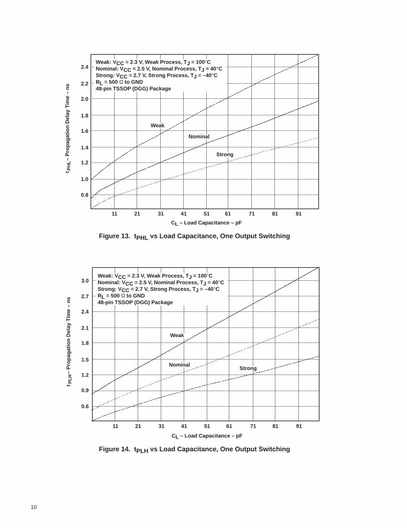
Switching Performance
Figures 11 through 16 present SPICE models of the device dynamic behavior. Propagation delay times across variousconditions of ambient temperature, load capacitance with one output switching, and load capacitance with 16 outputs switchingare shown.
1.28
1.26
1.24
1.22
1.20
1.18
1.16
1.14
1.12
1.10
8672584430162–12–26
– P
ropa
gatio
n D
elay
Tim
e –
nsP
HL
TJ – Junction Temperature – °C
One Output SwitchingNominal ProcessVCC = 2.5 VRL = 500 Ω, CL = 30 pF48-pin TSSOP (DGG) Package
VCC = 2.3 V
VCC = 2.5 V
VCC = 2.7 Vt
Figure 11. t PHL vs TJ
1.17
1.14
1.11
1.08
1.05
1.02
0.99
0.96
8672584430162–12–26
TJ – Junction Temperature – °C
One Output SwitchingNominal ProcessVCC = 2.5 VRL = 500 Ω, CL = 30 pF48-pin TSSOP (DGG) Package
VCC = 2.3 V
VCC = 2.5 V
VCC = 2.7 V
– P
ropa
gatio
n D
elay
Tim
e –
nsP
LHt
Figure 12. t PLH vs TJ
10
2.4
2.2
2.0
1.8
1.6
1.4
1.2
1.0
0.8
918171615141312111
CL – Load Capacitance – pF
Weak: VCC = 2.3 V, Weak Process, T J = 100°CNominal: V CC = 2.5 V, Nominal Process, T J = 40°CStrong: V CC = 2.7 V, Strong Process, T J = –40°CRL = 500 Ω to GND48-pin TSSOP (DGG) Package
Weak
Strong
Nominal
– P
ropa
gatio
n D
elay
Tim
e –
nsP
HL
t
Figure 13. t PHL vs Load Capacitance, One Output Switching
2.7
2.4
2.1
1.8
1.5
1.2
0.9
0.6
918171615141312111
3.0
CL – Load Capacitance – pF
Weak: VCC = 2.3 V, Weak Process, T J = 100°CNominal: V CC = 2.5 V, Nominal Process, T J = 40°CStrong: V CC = 2.7 V, Strong Process, T J = –40°CRL = 500 Ω to GND48-pin TSSOP (DGG) Package
Weak
StrongNominal
– P
ropa
gatio
n D
elay
Tim
e –
nsP
LHt
Figure 14. t PLH vs Load Capacitance, One Output Switching

11
2.4
2.2
2.0
1.8
1.6
1.4
1.2
1.0
0.8
918171615141312111
2.6
CL – Load Capacitance – pF
Weak: VCC = 2.3 V, Weak Process, T J = 100°CNominal: V CC = 2.5 V, Nominal Process, T J = 40°CStrong: V CC = 2.7 V, Strong Process, T J = –40°CRL = 500 Ω to GND48-pin TSSOP (DGG) Package
Weak
Strong
Nominal
– P
ropa
gatio
n D
elay
Tim
e –
nsP
HL
t
Figure 15. t PHL vs Load Capacitance, 16 Outputs Switching
2.8
2.4
2.0
1.6
1.2
0.8
0.4918171615141312111
3.2
CL – Load Capacitance – pF
Weak: VCC = 2.3 V, Weak Process, T J = 100°CNominal: V CC = 2.5 V, Nominal Process, T J = 40°CStrong: V CC = 2.7 V, Strong Process, T J = –40°CRL = 500 Ω to GND48-pin TSSOP (DGG) Package
Weak
StrongNominal
– P
ropa
gatio
n D
elay
Tim
e –
nsP
LHt
Figure 16. t PLH vs Load Capacitance, 16 Outputs Switching

12
Signal Integrity
Perhaps the most important measure of a device’s performance in the dynamic domain is the effect of varying conditions uponsignal integrity. Figures 17 through 20 show SPICE simulations of the device dynamic behavior. The effect of multiple outputsswitching simultaneously on one that is held at a valid logic level is shown (see Figures 17 and 18). The effects of slowinput-transition time (see Figure 19), and pin-to-pin skew (see Figure 20) are shown.
0
3.2
2.8
2.4
2.0
1.6
1.2
0.8
0.4
49484746454443
Time – ns
4241
15 Outputs Switching1 Quiet LowProcess = NominalTJ = 40°CRL = 500 ΩCL = 30 pF
VCC = 3.3 V
VCC = 2.5 V
VOLP at 3.3 VVOLP at 2.5 V
VOLV Are Approximately Equal
– O
utpu
t Vol
tage
– V
OV
Figure 17. Simultaneous-Switching Voltage (V OLP , VOLV) vs Time
0
3.2
2.8
2.4
2.0
1.6
1.2
0.8
0.4
2928272625242322212019
Time – ns
15 Outputs Switching1 Quiet HighProcess = NominalTJ = 40°CRL = 500 ΩCL = 30 pF
VCC = 3.3 V
VCC = 2.5 V
– O
utpu
t Vol
tage
– V
OV
Figure 18. Simultaneous-Switching Voltage (V OHP, VOHV) vs Time

13
2.4
2.1
1.8
1.5
1.2
0.9
0.6
0.3
1171091019385776961530
Time – ns
VCC = 2.5 VProcess = NominalTJ = 40°CRL = 500 ΩCL = 30 pF
16 Outputs Switching
– O
utpu
t Vol
tage
– V
OV
Figure 19. Slow Input-Transition Time
2.4
2.1
1.8
1.5
1.2
0.9
0.6
0.3
5046423834302622
<100 ps Nominal
0
VCC = 2.5 VProcess = NominalTJ = 40°C16 Outputs Switching
Time – ns
– O
utpu
t Vol
tage
– V
OV
Figure 20. Pin-to-Pin Skew (t PHL, tPLH) (<100 ps nominal)

14
Output Characteristics With DOC
Selecting a component with improved output drive characteristics simplifies the design engineer’s job of ensuring signalintegrity and meeting timing requirements. For signal integrity, the output must have an output impedance that minimizesovershoots and undershoots. A component with 26-Ω series damping resistors on the output ports was sometimes necessaryto improve the match of the impedance with the transmission-line load on the output of the buffer. The opposing characteristicthat must be considered is having sufficient drive to meet the timing requirements. The AVC family features TI’s DOC circuitthat automatically lowers the output impedance of the circuit during a signal transition and subsequently raises the impedanceto reduce overshoot and undershoot. Figures 21 and 22 contain typical voltage and current curves that illustrate the operationof the circuit as it transitions from one state to another.
3.2
2.8
2.4
2.0
1.6
1.2
0.8
0.4
1531361191028568513417
TJ = 40°CProcess = Nominal
IOL – Output Current – mA
VCC = 3.3 V
VCC = 2.5 V
VCC = 1.8 V
– O
utpu
t Vol
tage
– V
OL
V
1700
Figure 21. V OL vs IOL

15
2.8
2.4
2.0
1.6
1.2
0.8
0.4
–32–48–64–80–96–112–128–144 –16
TJ = 40°CProcess = Nominal
IOH – Output Current – mA
VCC = 3.3 VVCC = 2.5 V
VCC = 1.8 V
– O
utpu
t Vol
tage
– V
OH
V
–160 0
Figure 22. V OH vs IOH
The DOC circuitry provides enough drive current to achieve faster slew rates and meet timing requirements, but quicklyswitches the impedance level to reduce the overshoot and undershoot noise that is often found in high-speed logic. This featureof AVC logic eliminates the need for damping resistors in the output circuit, which are often used in series, and sometimesintegrated with logic devices, to limit electrical noise. Damping resistors reduce the noise, but increase propagation delay dueto the decreased drive current.
Because of the excellent signal integrity characteristics of the DOC output, transmission-line termination typically isunnecessary. Due to the high-impedance drive characteristics of the output in the static state, the use of dc termination isspecifically discouraged. The output current that is required to bias a dc termination network could exceed the static-stateoutput-drive capabilities of the device. AVC with DOC circuitry is ideally suited for any high-speed, point-to-point applicationor unterminated distributed load, such as high-speed memory interfacing.
Design Support
Examination of the characteristics of the device is a critical portion of a successful design. To aid the design engineer in analysisof device characteristics, the latest versions of IBIS models can be obtained from TI’s website at http://www.ti.com. SPICEmodels are also available from TI. Please contact your local TI field sales representative for more information.

16
Features and Benefits
Table 2 provides selected AVC family features and benefits.
Table 2. Selected AVC Family Features and Benefits
FEATURES BENEFITS
Optimized for 2.5-V VCC Enables low-power designs
Broad product offerings Simplifies component choice
Advanced EPIC fabrication process; turbo-circuit designSub-2-ns (maximum) speeds at 2.5 V.Easier to meet timing windowsin advanced high-speed designs
DOC outputs do not require series damping resistors internally or externallyReduced ringing without series output resistors,increased performance and cost savings
Bus-hold option Eliminates pullup or pulldown resistors on inputs
IOFF – reverse-current paths to VCC blocked on the inputs and outputsOutputs disabled during power off for use inpartial power down and mixed-voltage designs
Conclusion
For designs that require 1.8-V, 2.5-V, and 3.3-V logic functions with the highest performance, the AVC family provides thefastest, quietest logic devices optimized for 2.5-V and unterminated load conditions. AVC offers a broad line of Widebus andWidebus+ functions, logic gates, and octal bus-interface functions.
Acknowledgment
The authors of this application report are Stephen M. Nolan and Tim Ten Eyck.

17
Glossary
A
AVC Advanced very-low-voltage CMOS
C
CMOS Complementary metal-oxide semiconductor
D
DOC Dynamic output control (patent pending)
E
EPIC Enhanced-performance implanted CMOS
I
IBIS I/O buffer information specification
II Input current
II(hold) Input current (bus hold)
IOH High-level output current
IOL Low-level output current
L
LVTTL Low-voltage TTL (3.3-V power supply and interface levels)
P
PC Personal computer
S
SPICE Simulation program with integrated-circuit emphasis

18
T
tpd Propagation delay time
tPHL Propagation delay time, high- to low-level output
tPLH Propagation delay time, low- to high-level output
TSSOP Thin shrink small-outline package
TTL Transistor-transistor logic
V
VOH High-level output voltage
VOL Low-level output voltage
VOHP High-level output voltage peak
VOHV High-level output voltage valley
VOLP Low-level output voltage peak
VOLV Low-level output voltage valley

A–1
Appendix A – Parameter Measurement Information
VCC/2
VCC/2
VCC/2VCC/2
VCC/2VCC/2
VCC/2VCC/2
VOH
VOL
thtsu
From OutputUnder Test
CL = 30 pF(see Note A)
LOAD CIRCUIT
S1 Open
GND
1 kΩ
1 kΩ
OutputControl
(low-levelenabling)
OutputWaveform 1
S1 at 2 × VCC(see Note B)
OutputWaveform 2
S1 at GND(see Note B)
tPZL
tPZH
tPLZ
tPHZ
0 V
VOL + 0.15 V
VOH – 0.15 V
0 V
VCC
0 V
0 V
tw
VCCVCC
VOLTAGE WAVEFORMSSETUP AND HOLD TIMES
VOLTAGE WAVEFORMSPULSE DURATION
VOLTAGE WAVEFORMSENABLE AND DISABLE TIMES
TimingInput
DataInput
Input
tpdtPLZ/tPZLtPHZ/tPZH
Open2 × VCC
GND
TEST S1
NOTES: A. CL includes probe and jig capacitance.B. Waveform 1 is for an output with internal conditions such that the output is low except when disabled by the output control.
Waveform 2 is for an output with internal conditions such that the output is high except when disabled by the output control.C. All input pulses are supplied by generators having the following characteristics: PRR ≤ 10 MHz, ZO = 50 Ω, tr ≤ 2 ns, tf ≤ 2 ns.D. The outputs are measured one at a time with one transition per measurement.E. tPLZ and tPHZ are the same as tdis.F. tPZL and tPZH are the same as ten.G. tPLH and tPHL are the same as tpd.
0 V
VCC
VCC/2
tPHL
VCC/2 VCC/2VCC
0 V
VOH
VOL
Input
Output
VOLTAGE WAVEFORMSPROPAGATION DELAY TIMES
VCC/2 VCC/2
tPLH
2 × VCC
VCC
Figure A–1. AVC Parameter Measurement Information (1.8 V ± 0.15 V)

A–2
VCC/2
VCC/2
VCC/2VCC/2
VCC/2VCC/2
VCC/2VCC/2
VOH
VOL
thtsu
From OutputUnder Test
CL = 30 pF(see Note A)
LOAD CIRCUIT
S1 Open
GND
500 Ω
500 Ω
OutputControl
(low-levelenabling)
OutputWaveform 1
S1 at 2 × VCC(see Note B)
OutputWaveform 2
S1 at GND(see Note B)
tPZL
tPZH
tPLZ
tPHZ
0 V
VOL + 0.15 V
VOH – 0.15 V
0 V
VCC
0 V
0 V
tw
VCCVCC
VOLTAGE WAVEFORMSSETUP AND HOLD TIMES
VOLTAGE WAVEFORMSPULSE DURATION
VOLTAGE WAVEFORMSENABLE AND DISABLE TIMES
TimingInput
DataInput
Input
tpdtPLZ/tPZLtPHZ/tPZH
Open2 × VCC
GND
TEST S1
NOTES: A. CL includes probe and jig capacitance.B. Waveform 1 is for an output with internal conditions such that the output is low except when disabled by the output control.
Waveform 2 is for an output with internal conditions such that the output is high except when disabled by the output control.C. All input pulses are supplied by generators having the following characteristics: PRR ≤ 10 MHz, ZO = 50 Ω, tr ≤ 2 ns, tf ≤ 2 ns.D. The outputs are measured one at a time with one transition per measurement.E. tPLZ and tPHZ are the same as tdis.F. tPZL and tPZH are the same as ten.G. tPLH and tPHL are the same as tpd.
0 V
VCC
VCC/2
tPHL
VCC/2 VCC/2VCC
0 V
VOH
VOL
Input
Output
VOLTAGE WAVEFORMSPROPAGATION DELAY TIMES
VCC/2 VCC/2
tPLH
2 × VCC
VCC
Figure A–2. AVC Parameter Measurement Information (V CC = 2.5 V ± 0.2 V)

A–3
VOH
VOL
thtsu
From OutputUnder Test
CL = 30 pF(see Note A)
LOAD CIRCUIT
S12 × VCC
Open
GND
500 Ω
500 Ω
tPLH tPHL
OutputControl
(low-levelenabling)
OutputWaveform 1
S1 at 2 × VCC(see Note B)
OutputWaveform 2
S1 at GND(see Note B)
tPZL
tPZH
tPLZ
tPHZ
0 V
VOH
VOL
0 V
VOL + 0.3 V
VOH – 0.3 V
0 V
VCC
0 V
0 V
VCC
0 V
tw
Input
VOLTAGE WAVEFORMSSETUP AND HOLD TIMES
VOLTAGE WAVEFORMSPROPAGATION DELAY TIMES
VOLTAGE WAVEFORMSPULSE DURATION
VOLTAGE WAVEFORMSENABLE AND DISABLE TIMES
TimingInput
DataInput
Output
Input
tpdtPLZ/tPZLtPHZ/tPZH
Open2 × VCC
GND
TEST S1
NOTES: A. CL includes probe and jig capacitance.B. Waveform 1 is for an output with internal conditions such that the output is low except when disabled by the output control.
Waveform 2 is for an output with internal conditions such that the output is high except when disabled by the output control.C. All input pulses are supplied by generators having the following characteristics: PRR ≤ 10 MHz, ZO = 50 Ω, tr ≤ 2 ns, tf ≤ 2 ns.D. The outputs are measured one at a time with one transition per measurement.E. tPLZ and tPHZ are the same as tdis.F. tPZL and tPZH are the same as ten.G. tPLH and tPHL are the same as tpd.
VCC
VCC
VCC
VCC
VCC/2
VCC/2 VCC/2
VCC/2 VCC/2
VCC/2 VCC/2
VCC/2 VCC/2
VCC/2
VCC/2
VCC/2 VCC/2
Figure A–3. AVC Parameter Measurement Information (V CC = 3.3 V ± 0.3 V)

A–4