Embed Size (px)
Citation preview
adfm201604468.xml Generated by PXE using XMLPublishSM November 18, 2016 8:10 APT: WF JID: ADFMF
ullP
aper
adfm201604468(201604468)
Author Proofwww.afm-journal.de
Layer-Number-Dependent Optical Properties of 2DMaterials and Their Application for ThicknessDetermination
By Xiao-Li Li, Wen-Peng Han, Jiang-Bin Wu, Xiao-Fen Qiao, Jun Zhang,and Ping-Heng Tan*
The quantum confinement in atomic scale and the presence of interlayer coupling in
multilayer make the electronic and optical properties of 2D materials (2DMs) be
dependent on the layer number (N) from monolayer to multilayer. Optical properties of
2DMs have been widely probed by several optical techniques, such as optical contrast,
Rayleigh scattering, Raman spectroscopy, optical absorption, photoluminescence, and
second harmonic generation. Here, it has been reviewed how optical properties of several
typical 2DMs (e.g., monolayer and multilayer graphenes, transition metal
dichalcogenides) probed by these optical techniques significantly depend on N. Further, it
has been demonstrated how these optical techniques service as fast and nondestructive
approaches for N counting or thickness determination of these typical 2DM flakes. The
corresponding approaches can be extended to the whole 2DM family produced by
micromechanical exfoliations, chemical-vapor-deposition growth, or transfer processes
on various substrates, which bridges the gap between the characterization and
international standardization for thickness determination of 2DM flakes.
1. Introduction
2D materials (2DMs) can be usually exfoliated from layered ma-terials (LMs), which form strong chemical bonds in-plane butdisplay weak van der Waals (vdW) bonding out-of-plane.[1–3]
Up to now, 2DMs are explored to constitute a large familyincluding the graphene-like family, 2D dichalcogenides and2D oxides, of which physical properties range from insulators(BN,[4] HfS2,[5] etc.), topological insulators (Bi2Se3,[6, 7] Bi2Te3,[6]
etc.), semiconductors (MX2, M = Mo, W; X = S, Se),[8–10]
GaSe, GaS,[11] CuS, SnSe2, PbSnS2, GeSe, InSe,[12] SnS, ReSe2,etc.), semi-metals (graphene,[13] WTe2
[14, 15]) to superconduc-tors [3, 16](NbSe2, NbS2, FeSe, FeTe, etc.). The symmetriesof 2DM crystals include D6h (graphite, MX2, GaSe(S), CuS,SnS(Se)2, TaS(Se)2, FeTe(Se), NbSe2, and h-BN), D3d (SnSe2
and Bi2Te(Se)3), D2h (black phosphorus (BP),[17, 18] GeS(Se), andSnS(Se)), C2h (GaTe), and Ci (ReS(Se)2).[3] The lower symme-try (D2h, C2h, and Ci) leads to the in-plane anisotropy, which
X.-L. Li, W.-P. Han, J.-B. Wu, X.-F. Qiao, J. Zhang, P.-H. Tan,State Key Laboratory of Superlattices and Microstructures,Institute of Semiconductors, Chinese Academy of Sciences,Beijing 100083, ChinaJ. Zhang, P.-H. Tan, College of Materials Science andOpto-Electronic Technology, University of Chinese Academyof Science, Beijing 100049, ChinaCorrespondence to: P.-H. Tan (E-mail: [email protected])Q210.1002/adfm.201604468
brings one more degree of freedom than isotropic materialsand delivers various physical properties.[3] Two or more LMswith similar properties can be alloyed into an additional type of2DMs, namely, 2D alloy, which can offer tunable band gaps andthe corresponding amazing electronic and optical properties.[19]
These remarkable properties, including high mobility, highthermal conductivity, unique optical and mechanical proper-ties, and high specific surface area, can be found in 2DMs,which makes them be the ideal materials for promising appli-cations in nanoelectronics and optoelectronics devices.[20–31]
2DMs exhibit distinct electronic band structures due to thequantum confinement of electrons in 2D.[32–34] A single mono-layer (1L) of 2DMs is the thinnest nanosheet exfoliated fromits bulk counterpart, which can be from several micrometersto several centimeters in plane size but less than a nanome-ter in thickness.[1] The weak out-of-plane vdW bonding is ab-sent in 1L 2DMs. 1L graphene (1LG) is a typical 2DM withunique properties.[13, 32, 35–37] The rapid progresses of grapheneresearches have paved the way to experimental studies on other2DMs.[1–3, 8, 9, 38, 39] Unlike graphene, most of 1L 2DMs consistof more than one atomic element so that a single 1L of such2DMs usually consists of more than one atomic layers in whichthe two nearest atoms in adjacent atomic layers are also linkedvia strong chemical bonds. However, two or more 1L 2DMscan be coupled with each other by Van der Waals interactionto form multilayer (ML) 2DMs in a certain stacking orders.For instance, N layer (NL) graphenes (NLG, N > 2) can bestacked in a Bernal (AB) or rhombohedral (ABC) way or even a
Adv. Funct. Mater. 2016-11, 00, 1–18 c© 2016-11 WILEY-VCH Verlag GmbH & Co. KGaA, Weinheim wileyonlinelibrary.com 1
adfm201604468.xml Generated by PXE using XMLPublishSM November 18, 2016 8:10 APT: WF JID: ADFMF
ull
Pap
er
Author Proofwww.afm-journal.de
twisted way.[40–43] Exfoliated NL MX2 can exhibit two stackingways, i.e., 2H and 3R.[44–46] Even in anisotropic NL TMDs, suchas ReS2 and ReSe2, there still exist two stable categories,[47]
i.e., anisotropic-like (AI) and isotropic-like (IS), in terms oftheir stacking orders. In addition, these various 2DMs could beartificially restacked/assembled horizontally or vertically in achosen sequence to form vdW heterostructures, which can of-fer huge opportunities for designing the functionalities of suchheterostructures.[42, 43, 48–51] For a given stacking order, the elec-tronic band structures and lattice vibrations of the 2DMs aresignificantly N-dependent.[52] The band gap of 2H-MX2 exhibitsan indirect-to-direct transition from NL (N > 1) to 1L.[33, 53, 54]
The NL MoS2 FETs exhibit higher mobilities, more near-idealsubthreshold swings, and more robust current saturation overa large voltage window than 1L MoS2.[29] The direct band gapQ3of BP monotonically increases from bulk (0.2 eV) to 1L (1.5–2.0 eV), due to the strong interlayer coupling.[55, 56] In the caseof lattice vibrations, relative to 1L 2DMs, more atoms in theunit cell of NL (N > 1) 2DMs will result in more phononmodes in the zone-center of corresponding phonon dispersioncurves.[3, 10] Each mode in 1L 2DMs will split into N modes inNL 2DMs, named as Davydov components, whose frequenciesare determined by the interlayer coupling and the correspond-ing symmetry in NL 2DMs.[57, 58]
The N-dependent electronic and optical properties of2DMs[33, 52, 59] can be probed by various optical techniques,e.g., optical contrast (OC),[11, 60–63] Rayleigh scattering,[64] Ra-man spectroscopy,[3, 10, 65–67] optical absorption,[68] photolu-minescence (PL)[33, 47, 53, 55] and second harmonic generation(SHG).[69–71] With increasing N, the intensity, linewidth, orlineshape of the probed optical signals of 2DM flakes can be sig-nificantly modified, and some new optical features will emerge.For instance, with increasing N, the PL emission from directband gap of NL MoS2 flakes decreases in intensity while its peakposition almost keeps unchanged, however, new PL emissionfrom indirect band gap appears for N > 1 and this PL peakposition decreases toward lower energy with increasing N.[33]
Considering most of 2DM flakes are deposited on substrates,such as SiO2/Si, quartz or sapphire, the optical interferencebetween 2DM flakes and substrate must be considered in theoptical measurements, in which the SiO2 film thickness inSiO2/Si substrate and numerical aperture (NA) of the objec-tive used in microscope also affect the measurement resultsdependently.[72]
The sensitivity of optical properties of 2DM flakes on Ncan be utilized to identify N of the studied 2DM flakes oncethe relation between spectral parameters of optical propertiesand N is determined forehand. The thickness of 2DM flakesis a serial of discrete values. The thickness of an N layer 2DMflake is N times that of monolayer 2DM flake. In principle,once N of the 2DM flake is identified by optical techniques,its thickness is determined. In fact, atomic force microscopy(AFM) has been widely used to measure the thickness of 2DMflakes with a precision of 5%. The tapping mode is utilized tominimize sample damage.[57, 64, 72, 73] However, AFM techniqueis time-consuming and not suitable for a rapid measurementfor selected spots over a large area. AFM cannot also be usedfor suspended samples. The different interactions of the AFM
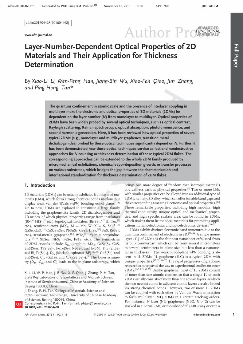
Figure 1. a) Optical image of 1LG, 3LG, and 4LG flakes. b)AFM image of 1LG and 4LG within the square frame in (a) andthe flake thickness measured by AFM. The instrumental offsetis ∼1.1 nm. Adapted with permission from Li et al.[72] c) Opticalimage of 1L, 4L, and 5L MoTe2. d) AFM image of the samples in(c) and the flake thickness measured by AFM. The instrumentaloffset is ∼4.0 nm. Adapted with permission from Song et al.[57]
Q4
tip with the flake and substrate will lead to large thicknessdiscrepancy for few-layer 2DM flakes.[57, 64, 72, 73] The offset be-tween 2DMs flake and substrate can be as large as severalnanometers, but the measured height difference between twoadjacent 2DM flakes is in good agreement with the correspond-ing thickness difference. For example, Figure 1 shows that, theinstrument offset for 1LG and 1L MoS2 is about 1.4 and 4.0nm, respectively. Optical techniques are fast and nondestruc-tive techniques for the probe of physical properties of 2DMflakes. Therefore, it is necessary to construct some reliable ap-proaches to precise identify N from the reported results basedon optical techniques.
Here, we review the recent advances in the N-dependentoptical properties of several typical 2DMs, such as NLGs, tran-sition metal dichalcogenides (e.g., 2H-MX2 (M = Mo, W; X =S, Se), and 1T-ReS(Se)2) probed by OC, Raman spectroscopy,PL, optical absorption spectroscopy, and SHG. The definiterelations between the optical properties and N by different op-tical techniques have been demonstrated for rapid and accurateidentification of the thickness or N of 2DM flakes. This reviewwill be expected to pave the ways to construct N-identificationtechniques of 2DM flakes based on optical techniques, benefitthe whole 2DM community for fundamental study, practicalapplications and quality appraisal for industrial products.
2 wileyonlinelibrary.com c© 2016-11 WILEY-VCH Verlag GmbH & Co. KGaA, Weinheim Adv. Funct. Mater. 2016-11, 00, 2–18
adfm201604468.xml Generated by PXE using XMLPublishSM November 18, 2016 8:10 APT: WF JID: ADFMF
ullP
aper
Author Proofwww.afm-journal.de
2. Optical Contrast
2DMs are usually transferred onto a kind of substrate, such asSi covered with a certain thickness of SiO2 film or quartz plate,for device application purpose.[13, 33] This causes a formation ofmultilayer structure containing air, 2DM flake and substrate.For the Si substrate covered by SiO2, the four layered structurecan be established, containing air(n0), NL 2DM(n1(8), d1),[74]
SiO2(n2(8), d2),[75] and Si(n3(8), d3), where ni (8) and di (i = 0,1, 2, 3) are the complex refractive index at specific wavelength(λ) and the thickness of each medium. When white-light of amicroscope is incident from air onto 2DM flakes on substrates,multiple reflections at the interfaces and optical interferencewithin the medium of the multilayer structures will modify thereflected light intensity from 2DM flakes relative to that directlyfrom the bare substrates. This makes the 2DM flakes can beeasily seen by naked eyes via microscope after they are trans-ferred onto substrates. The difference between reflected lightintensity from 2DM flakes deposited on substrate and from thebare substrate is known as OC of the 2DM flakes.[11, 60, 61, 76–78]
By using monochromatic illumination, 2DM flakes can beisolated from Si substrate covered with any SiO2 thickness(hSiO2
), albeit 300 nm for electronic devices and, especially, 90nm are most suitable for its visual detection.[60, 72] Because ofmultiple reflection interferences in the multilayer, OC of anNL 2DM flake on a substrate is dependent on the illuminationwavelength λ. The 2DM flake deposited on a given substrateexhibits a distinct OC(λ), which is significantly dependent on N.Besides N, OC(λ) is also sensitive to the NA of the objective usedin the microscope, which can be measured by a microscopecombined with a spectrometer.
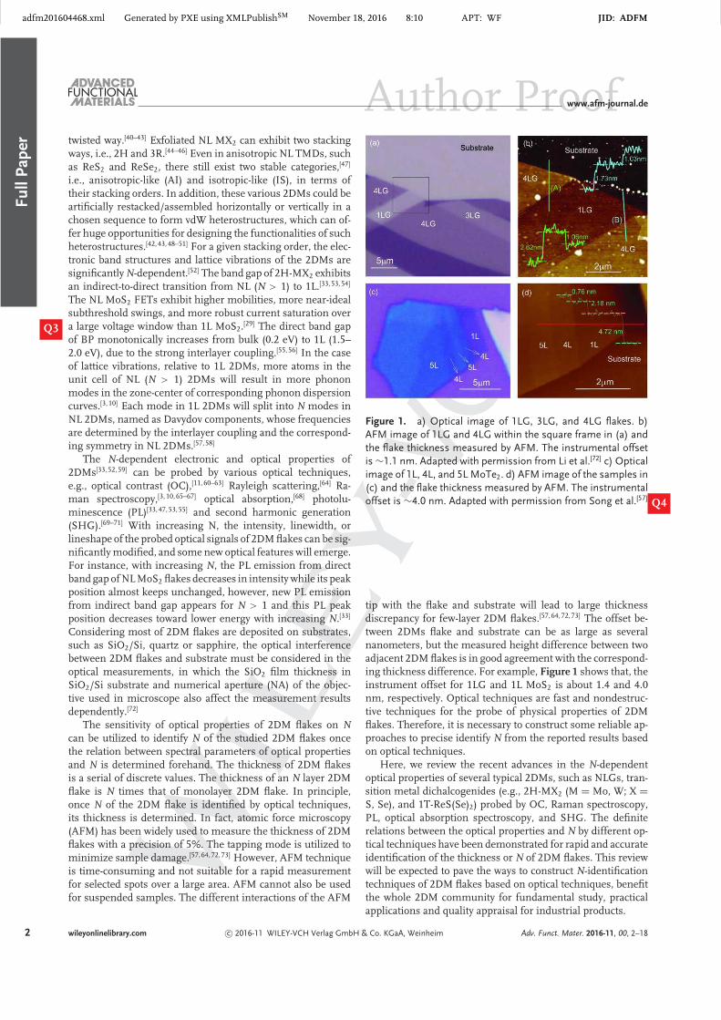
Figure 2 shows the schematic setup diagram to measureQ5OC(λ) of 2DM flakes by a microsystem in a backscatteringgeometry at room temperature, which is equipped with severalobjectives. OC(λ) is defined as[60, 61, 79]
OC(8) = 1 − R2dm+Sub(8)/RSub(8) (1)
where R2dm + Sub(λ) and RSub(λ) are the reflected intensitiesfrom the 2DM flakes on substrates and from the bare substrate,respectively. In some literatures, the OC(λ) also were definedas (R2dm + Sub(λ)-RSub(λ))/(R2dm + Sub(λ)+RSub(λ)).[11] Here, weuse the definition from Equation (Figure (1)). Tungsten halo-gen lamp can be used as a light source for reflection spec-tra measurement. The insets of Figure 2 show the measuredR2dm + Sub(λ), RSub(λ) and calculated OC(λ) by Figure (1) for2LG on SiO2/Si substrate (hSiO2
= 90 nm), respectively. OC(λ)can be quantitatively calculated by the multiple reflection in-terference method[60, 61, 79, 80] once the refractive index of 2DMsis known. The transfer-matrix method can be used to calculatetheoretical OC(λ),[79, 80] where the electric and magnetic fieldcomponents in each medium are associated by multiplicationof some characteristic matrices, dependent on the angle oflight, the medium thickness and the complex refractive indexof each medium. To reach a good agreement with the exper-imental data, the NA of the objective has to be considered.Because the incident and reflective lights are collected by thesame microscope objective with a given NA, all of the lights
Figure 2. Schematic diagram of the microscope system tomeasure OC(λ). For characterizing small flakes (few microns),a pinhole is needed to inset between the lamp and objectivein order to collect the reflection only from the desired flakefor a nonconfocal system. The collected reflection spectra frombare SiO2/Si substrate (h SiO2
= 90 nm) and from 2LG de-posited on substrate are shown in the inset (a) as RSub(λ)and R2dm + Sub(λ), respectively. The experimental OC(λ) = 1 −R2dm + Sub(λ)/RSub(λ) is depicted in the inset (b).
with an inclined angle in the field of objective rather than thelights only vertical to the NLG should be considered. Thus, thes-polarization (the incident light is polarized with its electricfield perpendicular to the plane containing the incident) andp-polarization (the incident light is polarized with its electricfield parallel to the plane of incidence) components should betreated separately in calculation.[80] Details of calculation hasbeen provided in Lu et al.[80]
Figure 3a shows the experimental OC(λ) values of a 10LGflake deposited on SiO2/Si substrate (hSiO2
= 89 nm) usingobjectives with NA = 0.25 (red), NA = 0.45 (green), and NA= 0.90 (blue), respectively. The maximum value of OC(λ) withNA = 0.90 is apparently smaller than those with NA = 0.25 andNA = 0.45, and the peak position exhibits a shift between anytwo of OC(λ). The experiments show that there exists a signif-icant discrepancy between experimental and theoretical OC(λ)for NA = 0.90[80] because the objective lens is not totally filledby incident light thus leading to a smaller effective NA.[64, 79]
The objective with NA ⋚ 0.55 is recommended to reach a goodagreement between experimental and theoretical OC(λ).[80] In-deed, For NA = 0.45, the experimental OC(λ) of 2LG, 3LG, and4LG for both hSiO2
= 89 nm (Figure 3b) and hSiO2= 286 nm
(Figure 3c) are in accordance with the theoretical ones calcu-lated by transfer-matrix method in the broad range of 400–800nm.
In general, OC(λ) of 2DM flakes on SiO2/Si substrates issignificantly dependent on N, NA, and hSiO2
. For 2DMs with aunified complex refractive index (n(8)) from monolayer to mul-tilayer, such as NLG, once hSiO2
and NA (20.55) are given, theexperimental OC(λ) is found to be in good agreement with thetheoretical ones. Therefore, OC(λ) can be adopted to identifyN of 2DM flakes with a unified n(8)), such as NLG. At first, to
Adv. Funct. Mater. 2016-11, 00, 3–18 c© 2016-11 WILEY-VCH Verlag GmbH & Co. KGaA, Weinheim wileyonlinelibrary.com 3

adfm201604468.xml Generated by PXE using XMLPublishSM November 18, 2016 8:10 APT: WF JID: ADFMF
ull
Pap
er
Author Proofwww.afm-journal.de
Figure 3. a) The experimental OC(λ) values of a 10LG flakedeposited on SiO2/Si (h SiO2
= 89 nm) using objectives withNA = 0.25 (red), NA = 0.45 (green), and NA = 0.90 (blue),respectively. The experimental OC(λ) and the calculated resultsof 2LG, 3LG, and 4LG for b) h SiO2
= 89 nm and c) h SiO2= 286
nm (c), NA = 0.45.
determine hSiO2by spectroscopic ellipsometer[81] or OC[80]; sec-
ond, to measure OC(λ) of the 2DM flake with NA (20.55); third,to calculate OC(λ) of NL 2DM flakes using known NA, hSiO2
andn(8)); finally, to check which N of the theoretical OC(λ) for NL2DM flakes is close to the experimental OC(λ) and determine N.Due to the advantages such a simple, efficient, nondestructive,and unnecessary of expensive and nonstandard equipment,OC technique is regarded as a good option for thickness or Nidentification of NLG.[60, 61, 79, 80] The accuracy of N identifica-tion depends on the OC(λ) difference between two flakes withadjacent N. The OC technique can be used to identify NLG upto N = 8.
Because absorption properties[54, 82] of ultrathin TMD flakesare significantly N-dependent on in the visible range due to thepresence of exciton effect, ultrathin TMD flakes are lack of aunified n(8) from monolayer to multilayer. Figure 4 shows theexperimental OC(λ) of 1-6L MoS2, which are also dependent onhSiO2
and NA. It is obvious that no common spectral featurescan be found within them. Therefore, it is hard to theoreticallyreproduce OC(λ) of TMD flakes with specific N to determineN for TMD flakes by comparing them with the experimentalones.
The 2DM flakes with different N usually display differentcolors in the optical images. Li et al.[63] have given the colordifference values between 1-15L 2DMs and substrate, includinggraphene, MoS2, WSe2, and TaS2, on SiO2/Si substrates (hSiO2
= 90 or 300 nm). These data were obtained from the brightnessprofile of color images or grayscale images of the red (R), green(G), or blue (B) channel in samples and substrates, can beaffected by illumination source, white balance, NA and hSiO2
.Because it is difficult to establish a relation between the colordifference and N for any NA and hSiO2
, it cannot be used toaccurately identify N of 2DM flakes for common conditionswith any white balance, NA and hSiO2
.
2.1. Rayleigh Scattering
Rayleigh scattering is the elastic scattering of light by particlesmuch smaller than the wavelength of the radiation. The parti-cles can be individual atoms. Under backscattering configura-
Figure 4. The experiment OC(λ) of 1-6L MoS2. The inset showsthe optical image of a flake with 3-7L MoS2.
tion, the scattered signal with same frequency as the laser ex-citation is the elastically scattered photons from Rayleigh scat-tering. The setup depicted in Figure 2 can be used to measureRayleigh signal once the lamp and spectrometer are replacedby a laser beam and a photon-counting avalanche photodiode,respectively.
Casiraghi et al.[64] have first given the Rayleigh scatteringcontrast method, as shown in Figure 5a,b. Figure 5a shows anoptical image of 1-3LG and 6LG prepared from micromechan-ical exfoliation of graphite and deposited on an SiO2/Si sub-strate (hSiO2
= 300 nm). Rayleigh scattering is performed withan inverted confocal microscope where an He–Ne laser (633nm) is used as the excitation source. Confocal Rayleigh imagesare obtained by raster scanning the sample. Figure 5b showsthe 3D confocal Rayleigh map for the NLG sample shown inFigure 5a. Rayleigh contrast was estimated by Equation (Figure(1)). The Rayleigh contrast appears to increase with N in certainwavelength ranges.[64] Rayleigh scattering can also be appliedto the CVD-grown NLG flakes, which are transferred onto theSiO2/Si substrate (hSiO2
= 90 nm).[83] Figure 5c shows the op-tical image of an CVD-grown flake, and its Rayleigh contrastmapping obtained by the 532 nm laser is shown in the Figure5d. It is found, the closer the measured spot is to the center ofthe CVD-grown flake, the higher the Rayleigh contrast is. Thisresults from more graphene layers grown at the flake center.
Because that multiple reflection interferences of both thelaser beam and Rayleigh signal still occur in the multilayercontaining air, 2DM flakes and substrate, the theoretical valueof Rayleigh contrast can also be calculated by the matrix transfermethod.[64] By comparing the experimental Rayleigh contrastof a 2DM flake with the theoretical one of 2DM flakes withdifferent N, one can identify N of NLG flakes. For example, fora multilayer graphene (MLG) flake grown by chemical vapordeposition, each graphene region with a definite N in the Figure5c was distinguished by the Rayleigh contrast mapping and wasmarked in the Figure 5d.
Because the laser excitation can be used for Rayleigh scatter-ing, the spatial resolution of the Rayleigh contrast is much bet-ter than that of OC measured by a collimated white-light beam.
4 wileyonlinelibrary.com c© 2016-11 WILEY-VCH Verlag GmbH & Co. KGaA, Weinheim Adv. Funct. Mater. 2016-11, 00, 4–18

adfm201604468.xml Generated by PXE using XMLPublishSM November 18, 2016 8:10 APT: WF JID: ADFMF
ullP
aper
Author Proofwww.afm-journal.de
Figure 5. Optical image of a) NLG with 1-3LG and 6LG pre-pared from micromechanical cleavage and the corresponding3D confocal Rayleigh imaging of b) NLG flakes by 633 nm ex-citation. Reproduced with permission from Casiraghi et al.[64]
Optical image of c) CVD-grown NLG flakes and the correspond-ing Rayleigh contrast mapping of d) the CVD-NLG flakes by 532nm excitation from which N of NLG flakes in different regionsis determined.
The spatial resolution of Rayleigh contrast can be down to thesize of the laser spot. In fact, the measured Rayleigh contrastby a laser source is a monochromatic OC with a wavelengthequal to that of the laser source. Therefore, to obtain a goodRayleigh contrast mapping, one should choose the laser exci-tation with an optimal wavelength at the maximum of OC(λ),e.g., ∼550 nm for NLG when hSiO2
= 90 or 300 nm. For NLMoS2, the optimal wavelength is ∼500 nm, as shown in theFigure 4. Around this wavelength, OC of NL MoS2 flakes aremuch sensitive of N than other wavelengths.
3. Raman Spectroscopy
Raman spectroscopy is the prime nondestructive characteriza-tion tool to probe the physical properties, such as phonons,electron–phonon coupling (EPC), band structures and inter-layer coupling of 2DMs.[10, 65, 84] Raman spectra of 2DMs con-sists of high- and ultralow-frequency Raman modes. The high-frequency modes are generally from in-plane vibrations, suchas D, G, and 2D mode in NLG[84] and E1
2g and A1g modes inNL MX2.[10] The ultralow-frequency (ULF) modes correspondto the relative motions of the planes themselves, either parallelor perpendicular to the plane, such as the shear (S) modes[67, 85]
and the LB modes,[85] which are related to the interlayer cou-pling. Moreover, the Si mode from SiO2/Si substrate under-neath NL 2DMs is hardly modified by defects and disorders inNL 2DMs, however, its intensity will be affected by the thick-
ness of 2DMs.[72, 86] High-frequency (HF) and ULF modes of2DMs and Raman modes from substrates can be strongly de-pendent on N in the peak position, profile, linewidth, and newHF and ULF modes will appear in the Raman spectra of 2DMs.
3.1. HF Raman Modes of 2DMs
3.1.1. N-Dependent Frequency
HF Raman modes have been deeply investigated in NLG andgraphite materials, providing useful information on the defects(by D band), in-plane vibration of sp2 carbon atoms (by Gband) as well as the stacking order (by 2D band). The HFRaman spectrum of the intrinsic NLG consists of G (∼1580cm−1) and 2D (∼2670 cm−1) modes.[66, 84] The G peak originatesfrom in-plane vibration of sp2 carbon atoms and is due to thedoubly degenerate zone center E2g mode. The 2D band is thesecond order of the D peak, where D peak comes from TOphonons around the Brillouin Zone edge near K, is active bydouble resonance process.[84] Because the interlayer coupling ismuch weaker than the intralayer C–C bonding, the interlayercoupling almost does not affect the intralayer C–C bondingin NLG. Therefore, it is revealed that the peak position (orfrequency) of the G mode, Pos(G), is almost insensitive to N.[67]
However, the profile of the 2D mode is strongly dependent on Nof NLG. Here, we will first discuss the 2D profile of AB-stackedNLG as a function of N.
Because the 2D band originates from a two-phonon doubleresonance Raman process, it is closely related to the band struc-ture of graphene layers. 1LG has a single and sharp 2D band,but the 2D band of NL graphenes can be fitted by multipleLorentzian peaks, due to the multiple resonance Raman pro-cesses related with the electronic band structure of NLGs. Fer-rari et al.[66] have successfully explained the changes of the 2Dband in shape, linewidth, and peak position for graphene andgraphene layers. The 2D mode is dispersive.[41, 87] The Pos(2D)and line shape of 2D mode depend on the excitation energy.Zhao et al.[87] have demonstrated that the changes of the 2Dbands can be used to clearly identified 1LG and 2-4LG with ABstacking once the excitation wavelength is 633 nm. The Ramanspectra of 1-5LG measured with 633 nm laser excitation areshown in Figure 6.[87] The 2D bands of AB-stacked 2LG, 3LGand 4LG can be fitted with 4, 7, 8 Lorentzian peaks, respec-tively. The characteristic peaks of each band are shown by thearrows, stars and pluses. However, for more than five graphenelayers, the difference between their Raman spectra is insuf-ficient to accurately distinguish them. Because the differentcomponents of the 2D bands may exhibit different resonantbehaviors dependent on laser wavelength, it is very impor-tant to choose an appropriate laser wavelength to identify N ofNLG.[87] Moreover, the line shape of 2D mode also depends onthe stacking order of graphene.[41] For example, the 2D peak ofABC-stacked 3LG under excitation of 633 nm also can be fittedby seven Lorentzian peaks like as that of AB-stacked 3LG, how-ever, the clear blueshifts of the subpeaks, especially those ofhigher frequencies for the ABC-stacked 3LG probe the differ-ence of band structure between AB- and ABC-stacked 3LG.[41, 88]
The 2D band of ABC-stacked NLG also shows an N-dependentbehavior.[40, 41, 88]
Adv. Funct. Mater. 2016-11, 00, 5–18 c© 2016-11 WILEY-VCH Verlag GmbH & Co. KGaA, Weinheim wileyonlinelibrary.com 5

adfm201604468.xml Generated by PXE using XMLPublishSM November 18, 2016 8:10 APT: WF JID: ADFMF
ull
Pap
er
Author Proofwww.afm-journal.de
Figure 6. Raman spectra of a) G and 2D peaks of 1-3LG andb) those of 4LG and 5LG excited by the 633 nm laser. Adaptedwith permission from Zhao et al.[87]
2H-MX2 is a subject of intense researches because ofits electronic and optical properties, such as strong PL,[33, 53]
electroluminescence (EL),[89] controllable valley and spinpolarization.[90–92] A 1L MX2 consists of two planes of hexago-nally arranged X atoms linked to a hexagonal plane of M atomsvia covalent bonds. In the NL MX2, individual MX2 layers areheld together by weak vdW forces. The change of symmetryand atoms in unit cell with N and the presence of interlayercoupling in NL MX2 (N > 2) make the high-frequency modesof NL MX2 be dependent on N.
Figure 7a,b shows the high-frequency Raman spectra of 1-10L MoS2 measured by 532 nm excitation and that of 1-8L WS2
under 488 nm excitation, respectively. The high-frequency Ra-man spectra of bulk MX2 consist mainly of the E1
2g and A1g
modes. Because of the different symmetries between even andodd NL MX2 and bulk MX2, these two modes in bulk MX2
should be assigned as the E′ and A′1 in odd NL (ONL) MX2
and the Eg and A1g modes in even NL (ENL) MX2,[10, 59, 93] re-spectively. However, to see the evolution from 1L to NL (N> 1), hereafter the two modes for all cases are simply labeledas E1
2g and A1g, as commonly done in the literatures.[10, 94–96]
Figure 7a shows that E12g and A1g mode is respectively located
at ≈380 and ≈402cm−1 in MoS2. With increasing N, the fre-quency of the E1
2g mode, Pos(E12g), decreases and that of the
A1g mode, Pos(A1g), increases. The frequency difference 1ω(A− E) = Pos(A1g)-Pos(E1
2g) increases from 17.4 cm−1 for 1Lto 25 cm−1 for 10L, following the formula of 1ω(A − E) =25.8 − 8.4/N,[10] as shown in Figure 7c. The different trend ofPos(E1
2g) and Pos(A1g) with N is attributed to the surface effectas the larger force constants at the surface of the thin film canmake a difference.[97] It is found that the nearest vdW interac-tions can significantly affect the frequency of the HF phononmodes in NL MX2.[57]
Similar anomalous frequency difference between the E12g
and A1g modes with increasing layer number also exists in other
Figure 7. HF Raman modes of 1-10L MoS2 a) measured by532 laser and those of 1-8L WS2 b) at 488 laser. The frequencyof the E1
2g and A1g modes and their difference with increasingN of c) NL MoS2 and d) NL WS2.
2D MX2. However, the E12g and A1g modes of WS2 are found to
be not so sensitive to N.[98, 99] Figure 7d shows that E12g and A1g
mode is respectively located at ≈356 and ≈419 cm−1 in WS2.The frequency shift of both E1
2g and A1g modes for NL WS2
(shown in Figure 7d) is less than 3 cm−1. The case of E12g and
A1g modes in WSe2 is more complicated. E12g and A1g modes
overlap each other at ≈248 cm−1. The E12g mode is very weak
and can be revealed under cross (HV) polarization configura-tion according to polarization properties of E2g peak observableunder both the parallel (VV) and HV polarization configurationwhile A1g observable under VV polarization configuration.
Anisotropic 2DMs, such as ReS2, offer one more dimensionthan isotropic 2DMs to tune their physical properties. The bulkand 1L ReS2 belong to the Ci space group. The crystal structureof ReS2 is much more complicated than graphene and MX2.Its unit cell contains four formula units consisting of two cat-egories of Re atoms together with four categories of S atoms.Each Re has six neighboring S sites, and the Re atoms are sand-wiched by the S atoms at both sides. Because the unit cell of 1LReS2 comprised 12 atoms, it has 36 normal vibrational modes.The Ŵ phonons of 1L ReS2 can be expressed by the irreduciblerepresentations of Ci as follows: Ŵ = 18(A
′′ + A′).[47, 100, 101]
In principle, for the NL ReS2 with a unit cell of 12N atoms,36N modes are expected. There are two stable stacking orders,namely isotropic-like (IS) and anisotropic-like (AI), in the NLReS2.[47] We summarize the high-frequency Raman spectra ofAI- and IS-NL-ReS2 up to 8L from a range of 120-250 cm−1
in Figure 8a,b, respectively, together with that of 1L ReS2 forcomparison.[47] The number of modes does not significantlychange with N increasing from 1L to 8L. The relative intensity
6 wileyonlinelibrary.com c© 2016-11 WILEY-VCH Verlag GmbH & Co. KGaA, Weinheim Adv. Funct. Mater. 2016-11, 00, 6–18
adfm201604468.xml Generated by PXE using XMLPublishSM November 18, 2016 8:10 APT: WF JID: ADFMF
ullP
aper
Author Proofwww.afm-journal.de
Figure 8. HF Raman spectra of a) AI- and b) IS-NL-ReS2 upto 8L in the range of 120–250 cm−1. c) Pos(mb)-Pos(ma) as afunction of N for AI-stacked (green circles) and IS-stacked (redcircles) 2–8L ReS2. The inset shows the atom displacement ofthe modes ma and mb. Reproduced with permission from Qiaoet al.[47]
between different modes is usually sample dependent, owingto the relative orientation between NL ReS2 crystal axis andlaser polarization direction. The peaks at ≈161, ≈213, ≈235cm−1 do not appreciably move with respect to N for both AI-and IS-NL-ReS2. However, as marked by the dashed lines inFigure 8a,b, the ma and mb peaks have different N-dependentevolution tendencies in AI- and IS-NL-ReS2. The vibrationaldisplacements of ma and mb mode are Ag-like out-of-planeand Eg-like in-plane mode, respectively, analogous to thosein NL MX2. The ma mode of 1L ReS2 softens in AI-stackedNL ReS2 while it stiffens for IS-stacked ones. Unlike the mamode, the mb mode stiffens in AI-stacked NL ReS2 but almostremains unmoved for all IS-stacked samples. Consequently,1ω(mb − ma) = Pos(mb) − Pos(ma) increases from 16.7 cm−1
of 1L ReS2 to 20.6 cm−1 of AI-8L-ReS2, but decreases to 13.3cm−1 of IS-8L-ReS2, as plotted in Figure 8c.
All the 2DM flakes are bonded together by the vdW coupling.The HF Raman peaks of NL 2DM flakes should always exhibitfrequency shifts from bulk to monolayer, either significantly orinsensitively dependent on N. Once the frequency of HF modesor frequency difference between two HF modes of NL 2DMflakes is sensitive to N, it can be applied for N identification for2DM flakes, such as the position and profile of the 2D modesin NLG, Pos(A1g)-Pos(E1
2g) in NL MoS2 and 1ω(mb − ma) inNL ReS2. However, for almost all the 2DM flakes, when N> 5, the frequency difference of HF modes between NL and(N+1)L 2DM flakes, so in this case, it is no longer valid for Nidentification. The HF Raman peaks always exhibit frequencyshifts from bulk to monolayer, which has been observed inother 2DMs, such as Bi2Se3, Bi2Te3, PtS2, WTe2, GaS, andGaSe.[3, 11, 102–104]
3.1.2. N-Dependent Peak Intensity
In the simplest model, the Raman intensity of HF modes inNL 2DMs would increase with N, because there are more 2Dlayers to contribute the Raman signal. However, the thicker2DM flake also causes the stronger absorption of the laserbeam and Raman signal. Thus, after a critical N, the Ramanintensity of HF modes in NL 2DMs would decrease with N.
Again, we take NLG as an example. 22 intrinsic NLG flakeswith N from 1 to 102 are deposited on (different) SiO2/Si sub-
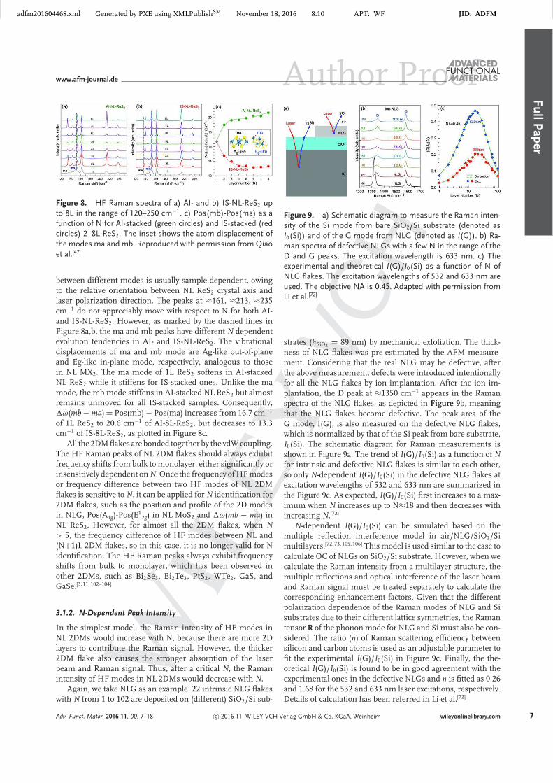
Figure 9. a) Schematic diagram to measure the Raman inten-sity of the Si mode from bare SiO2/Si substrate (denoted asI0(Si)) and of the G mode from NLG (denoted as I(G)). b) Ra-man spectra of defective NLGs with a few N in the range of theD and G peaks. The excitation wavelength is 633 nm. c) Theexperimental and theoretical I(G)/I0(Si) as a function of N ofNLG flakes. The excitation wavelengths of 532 and 633 nm areused. The objective NA is 0.45. Adapted with permission fromLi et al.[72]
strates (hSiO2= 89 nm) by mechanical exfoliation. The thick-
ness of NLG flakes was pre-estimated by the AFM measure-ment. Considering that the real NLG may be defective, afterthe above measurement, defects were introduced intentionallyfor all the NLG flakes by ion implantation. After the ion im-plantation, the D peak at ≈1350 cm−1 appears in the Ramanspectra of the NLG flakes, as depicted in Figure 9b, meaningthat the NLG flakes become defective. The peak area of theG mode, I(G), is also measured on the defective NLG flakes,which is normalized by that of the Si peak from bare substrate,I0(Si). The schematic diagram for Raman measurements isshown in Figure 9a. The trend of I(G)/I0(Si) as a function of Nfor intrinsic and defective NLG flakes is similar to each other,so only N-dependent I(G)/I0(Si) in the defective NLG flakes atexcitation wavelengths of 532 and 633 nm are summarized inthe Figure 9c. As expected, I(G)/I0(Si) first increases to a max-imum when N increases up to N≈18 and then decreases withincreasing N.[72]
N-dependent I(G)/I0(Si) can be simulated based on themultiple reflection interference model in air/NLG/SiO2/Simultilayers.[72, 73, 105, 106] This model is used similar to the case tocalculate OC of NLGs on SiO2/Si substrate. However, when wecalculate the Raman intensity from a multilayer structure, themultiple reflections and optical interference of the laser beamand Raman signal must be treated separately to calculate thecorresponding enhancement factors. Given that the differentpolarization dependence of the Raman modes of NLG and Sisubstrates due to their different lattice symmetries, the Ramantensor R of the phonon mode for NLG and Si must also be con-sidered. The ratio (η) of Raman scattering efficiency betweensilicon and carbon atoms is used as an adjustable parameter tofit the experimental I(G)/I0(Si) in Figure 9c. Finally, the the-oretical I(G)/I0(Si) is found to be in good agreement with theexperimental ones in the defective NLGs and η is fitted as 0.26and 1.68 for the 532 and 633 nm laser excitations, respectively.Details of calculation has been referred in Li et al.[72]
Adv. Funct. Mater. 2016-11, 00, 7–18 c© 2016-11 WILEY-VCH Verlag GmbH & Co. KGaA, Weinheim wileyonlinelibrary.com 7
adfm201604468.xml Generated by PXE using XMLPublishSM November 18, 2016 8:10 APT: WF JID: ADFMF
ull
Pap
er
Author Proofwww.afm-journal.de
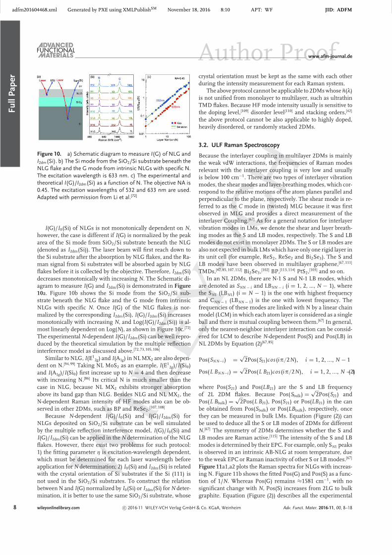
Figure 10. a) Schematic diagram to measure I(G) of NLG andI2dm(Si). b) The Si mode from the SiO2/Si substrate beneath theNLG flake and the G mode from intrinsic NLGs with specific N.The excitation wavelength is 633 nm. c) The experimental andtheoretical I(G)/I2dm(Si) as a function of N. The objective NA is0.45. The excitation wavelengths of 532 and 633 nm are used.Adapted with permission from Li et al.[72]
I(G)/I0(Si) of NLGs is not monotonically dependent on N,however, the case is different if I(G) is normalized by the peakarea of the Si mode from SiO2/Si substrate beneath the NLG(denoted as I2dm(Si)). The laser beam will first reach down tothe Si substrate after the absorption by NLG flakes, and the Ra-man signal from Si substrates will be absorbed again by NLGflakes before it is collected by the objective. Therefore, I2dm(Si)decreases monotonically with increasing N. The Schematic di-agram to measure I(G) and I2dm(Si) is demonstrated in Figure10a. Figure 10b shows the Si mode from the SiO2/Si sub-strate beneath the NLG flake and the G mode from intrinsicNLGs with specific N. Once I(G) of the NLG flakes is nor-malized by the corresponding I2dm(Si), I(G)/I2dm(Si) increasesmonotonically with increasing N, and Log(I(G)/I2dm(Si)) is al-most linearly dependent on Log(N), as shown in Figure 10c.[72]
The experimental N-dependent I(G)/I2dm(Si) can be well repro-duced by the theoretical simulation by the multiple reflectioninterference model as discussed above.[72, 73, 105, 106]
Similar to NLG, I(E12g) and I(A1g) in NL MX2 are also depen-
dent on N.[94, 99] Taking NL MoS2 as an example, I(E12g)/I(Si0)
and I(A1g)/I(Si0) first increase up to N = 4 and then decreasewith increasing N.[86] Its critical N is much smaller than thecase in NLG, because NL MX2 exhibits stronger absorptionabove its band gap than NLG. Besides NLG and NL MX2, theN-dependent Raman intensity of HF modes also can be ob-served in other 2DMs, such as BP and ReSe2.[107, 108]
Because N-dependent I(G)/I0(Si) and I(G)/I2dm(Si) forNLGs deposited on SiO2/Si substrate can be well simulatedby the multiple reflection interference model, I(G)/I0(Si) andI(G)/I2dm(Si) can be applied in the N determination of the NLGflakes. However, there exist two problems for such protocol:1) the fitting parameter η is excitation-wavelength dependent,which must be determined for each laser wavelength beforeapplication for N determination; 2) I0(Si) and I2dm(Si) is relatedwith the crystal orientation of Si substrates if the Si (111) isnot used in the SiO2/Si substrates. To construct the relationbetween N and I(G) normalized by I0(Si) or I2dm(Si) for N deter-mination, it is better to use the same SiO2/Si substrate, whose
crystal orientation must be kept as the same with each otherduring the intensity measurement for each Raman system.
The above protocol cannot be applicable to 2DMs whose n(8)is not unified from monolayer to multilayer, such as ultrathinTMD flakes. Because HF mode intensity usually is sensitive tothe doping level,[109] disorder level[110] and stacking orders,[42]
the above protocol cannot be also applicable to highly doped,heavily disordered, or randomly stacked 2DMs.
3.2. ULF Raman Spectroscopy
Because the interlayer coupling in multilayer 2DMs is mainlythe weak vdW interactions, the frequencies of Raman modesrelevant with the interlayer coupling is very low and usuallyis below 100 cm−1. There are two types of interlayer vibrationmodes, the shear modes and layer-breathing modes, which cor-respond to the relative motions of the atom planes parallel andperpendicular to the plane, respectively. The shear mode is re-ferred to as the C mode in (twisted) MLG because it was firstobserved in MLG and provides a direct measurement of theinterlayer Coupling.[67] As for a general notation for interlayervibration modes in LMs, we denote the shear and layer breath-ing modes as the S and LB modes, respectively. The S and LBmodes do not exist in monolayer 2DMs. The S or LB modes arealso not expected in bulk LMs which have only one rigid layer inits unit cell (for example, ReS2, ReSe2 and Bi2Se3). The S andLB modes have been observed in multilayer graphene,[67, 111]
TMDs,[47, 85, 107, 112] Bi2Se3,[102] BP,[113, 114] PtS2,[103] and so on.In an NL 2DMs, there are N-1 S and N-1 LB modes, which
are denoted as SNN − i and LBNN − i (i = 1, 2, ..., N − 1), wherethe SN1 (LBN1) (i = N − 1) is the one with highest frequencyand CNN − 1 (LBNN − 1) is the one with lowest frequency. Thefrequencies of these modes are linked with N by a linear chainmodel (LCM) in which each atom layer is considered as a singleball and there is mutual coupling between them.[67] In general,only the nearest-neighbor interlayer interaction can be consid-ered for LCM to describe N-dependent Pos(S) and Pos(LB) inNL 2DMs by Equation (2)[67, 85]
Pos(SNN−i ) =√
2Pos(S21)cos (iB/2N), i = 1, 2, ..., N − 1
Pos(L BNN−i ) =√
2Pos(L B21)cos (iB/2N), i = 1, 2, ..., N − 1(2)
where Pos(S21) and Pos(LB21) are the S and LB frequencyof 2L 2DM flakes. Because Pos(Sbulk) =
√2Pos(S21) and
Pos(L Bbulk) =√
2Pos(L B21), Pos(S21) or Pos(LB21) in the canbe obtained from Pos(Sbulk) or Pos(LBbulk), respectively, oncethey can be measured in bulk LMs. Equation (Figure (2)) canbe used to deduce all the S or LB modes of 2DMs for differentN.[67] The symmetry of 2DMs determines whether the S andLB modes are Raman active.[115] The intensity of the S and LBmodes is determined by their EPC. For example, only SN1 peaksis observed in an intrinsic AB-NLG at room temperature, dueto the weak EPC or Raman inactivity of other S or LB modes.[67]
Figure 11a1,a2 plots the Raman spectra for NLGs with increas-ing N. Figure 11b shows the fitted Pos(G) and Pos(S) as a func-tion of 1/N. Whereas Pos(G) remains ≈1581 cm−1, with nosignificant change with N, Pos(S) increases from 2LG to bulkgraphite. Equation (Figure (2)) describes all the experimental
8 wileyonlinelibrary.com c© 2016-11 WILEY-VCH Verlag GmbH & Co. KGaA, Weinheim Adv. Funct. Mater. 2016-11, 00, 8–18
adfm201604468.xml Generated by PXE using XMLPublishSM November 18, 2016 8:10 APT: WF JID: ADFMF
ullP
aper
Author Proofwww.afm-journal.de
Figure 11. a1) Stokes/anti-Stokes Raman spectra for the Speak spectral region and a2) Stokes Raman spectra for the Gpeak spectral region. b) Pos(G) (filled black circles) and Pos(S)(open blue circles), as a function of 1/N. The red dash-dottedline is a plot of Equation (Figure (2)). Vertical dashed lines in(a1) and the horizontal line in (b) are guides to the eye. Adaptedwith permission from Tan et al.[67]
data. The only unknown parameter in Equation (Figure (2))is the interlayer coupling strength. By fitting the experimen-tal data we can directly measure it. This result indicates thatthe interlayer coupling strength is constant in NLGs and inde-pendent on N. In Bernal-stacked MLG, the hardening of the Smode is not due to a variation of interlayer coupling, but ratherto an increase of the overall restoring force (surface layers areless bound than in the bulk) going from 2LG to bulk graphite.
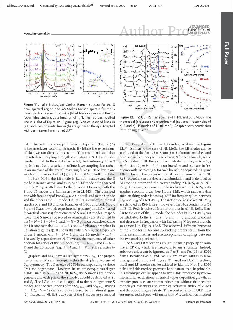
In bulk MoS2, the LB mode is Raman inactive and the Smode is Raman active, and thus, one ULF mode only observedin bulk MoS2 is attributed to the S mode. However, both theS and LB modes are Raman active in 2L MX2. The observedone with frequency of Pos(Sbulk)/
√2 is attributed to the S mode
and the other is the LB mode. Figure 12a shows experimentalspectra of S and LB phonon branches of 1-10L and bulk MoS2.Figure 12b,c show their experimental (squares) and LCM-basedtheoretical (crosses) frequencies of S and LB modes, respec-tively. The S modes observed experimentally are attributed tothe i = N − 1, i = N − 3, and i = N − 5 phonon branches, whilethe LB modes to the i = 1, i = 3, and i = 5 phonon branches inEquation (Figure (2)). It shows that when N > 6, the frequencyof the S modes with i = N − 1 and the LB modes with i =1 is weakly dependent on N. However, the frequency of otherphonon branches of the S modes (e.g., i = N − 3 and i = N −5) and the LB modes (e.g., i = 3 and i = 5) is still sensitive toN.
graphite and MX2 have a high symmetry (D6h) The proper-ties of these LMs are isotropic within the ab plane because ofD6h symmetry. The S modes of 2DMs corresponding to theseLMs are degenerate. However, in an anisotropic multilayer2DMs, such as NL BP and NL ReS2, the S modes are nonde-generate and each pair of the S modes should be denoted as Sx
and Sy. The LCM can also be applied to the nondegenerate Smodes, and the frequencies of the Sx
N, N − j and SyN, N − j modes
(j = 1,2,...,N − 1) can also be expressed by Equation (Figure(2)). Indeed, in NL ReS2, two sets of the S modes are observed
Figure 12. a) ULF Raman spectra of 1-10L and bulk MoS2. Thetheoretical (crosses) and experimental (squares) frequencies ofb) S and c) LB modes of 1-10L MoS2. Adapted with permissionfrom Zhang et al.[85]
in 2-8L ReS2 along with the LB modes, as shown in Figure13a.[47] Similar to the case of NL MoS2, the LB modes can beattributed to the j = 1, j = 3, and j = 5 phonon branches anddecrease in frequency with increasing N for each branch, whilethe S modes in NL ReS2 can be attributed to the j = N − 1, j= N − 3, and j = N − 5 phonon branches and increase in fre-quency with increasing N for each branch, as depicted in Figure13b,c. This stacking order is most stable and anisotropic in NLReS2 according to the theoretical simulation and is denoted asAI-stacking order and the corresponding NL ReS2 as AI-NL-ReS2. However, only one S mode is observed in 2L ReS2 withanother stacking order (see Figure 13d), which suggests thatsuch stacking order is isotropic.[47] Its frequency lies betweenSx
21 and Sy21 of AI-2L-ReS2. The isotropic-like stacked NL ReS2
are denoted as IS-NL-ReS2. However, the N-dependent Pos(S)in IS-NL-ReS2 is quite different from that in AI-NL-ReS2. Sim-ilar to the case of the LB mode, the S modes in IS-NL-ReS2 canbe attributed to the j = 1, j = 3 and j = 5 phonon branchesand decrease in frequency with increasing N for each branch,as depicted in Figure 13e,f. The observed different branchesof the S modes in AI- and IS-stacking orders result from thedifferent symmetries and electron-phonon couplings betweenthe two stacking orders.[47]
The S and LB vibrations are an intrinsic property of mul-tilayer 2DMs, which are irrelevant to any substrate. Indeed,substrate effect can be ignored on Pos(S) and Pos(LB) of 2DMflakes. Because Pos(S) and Pos(LB) are linked with N by a ro-bust general formula of Figure (2) based on LCM, therefore,the S and LB modes can be utilized to identify N of NL 2DMflakes and this method proves to be substrate-free. In principle,this technique can be applied to any 2DMs produced by micro-mechanical exfoliations, chemical-vapor-deposition growth, ortransfer processes on various substrates, without the need formonolayer thickness and complex refractive index of 2DMsand the supporting substrate. The recent advance in ULF mea-surement techniques will make this N-identification method
Adv. Funct. Mater. 2016-11, 00, 9–18 c© 2016-11 WILEY-VCH Verlag GmbH & Co. KGaA, Weinheim wileyonlinelibrary.com 9
adfm201604468.xml Generated by PXE using XMLPublishSM November 18, 2016 8:10 APT: WF JID: ADFMF
ull
Pap
er
Author Proofwww.afm-journal.de
Figure 13. Low-frequency Raman spectra of 1-8L ReS2 with a)AI-stacking and b) IS-stacking orders. The theoretical (crosses)and experimental (squares, circles and triangles) frequenciesof c) LB mode and d) C mode with AI-stacking order and e)LB mode and f) C mode with IS-stacking order in 2-8L ReS2.Reproduced with permission from Qiao et al.[47]
as a robust, fast, nondestructive and substrate-free approachfor layer-number identification of ultrathin 2DM flakes.
The N-identification of NL 2DM flakes by ULF Ramanmodes can be also applied to 2D alloys, which can be alloyedby any of two or more 2DMs with similar properties. Here, wetake Mo0.5W0.5S2 alloys (simply denoted as MoWS2 alloy) asan example to show how to identify N of MoWS2 alloy flakesdirectly by the S mode of bulk alloy. In comparison to NL WS2
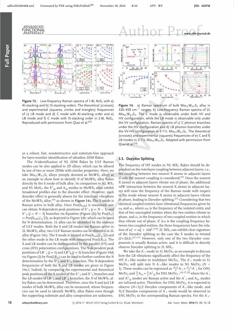
and NL MoS2, the E12g and A1g modes in MoWS2 alloy exhibit
broadened profiles due to the disorder effect. However, suchdisorder effect is generally absent for the interlayer vibrationsof the MoWS2 alloy,[19] as shown in Figure 14a. The S mode isRaman active in bulk alloy. Once Pos(Sbulk) is measured, onecan obtain N-dependent peak positions of S+
2 (j = N − 1) andS+
6 (j = N − 3) branches via Equation (Figure (2)) by Pos(S21)= Pos(Sbulk)/
√
(2), as depicted in Figure 14b, which can be usedfor N determination. 1L alloy can be identified by the absenceof ULF modes. Both the S and LB modes are Raman active in2L MoWS2 alloy, two ULF Raman modes can be observed in 2Lalloy (Figure 14c). The S mode is located at Pos(Sbulk)/
√
(2) andthe other mode is the LB mode with measured Pos(LB21). TheS and LB modes can be distinguished by the parallel (VV) andcross (HV) polarization configurations. The N-dependent peakpositions of LB−
2 (j = 1) and LB−6 (j = 3) branches (Figure 14d)
via Figure (2) by Pos(LB21) can be used to further confirm the Ndetermination by the S+
2 and S+6 branches. The N-dependent
frequencies of both the S and LB modes are given in Figure14e,f. Indeed, by comparing the experimental and theoreticalpeak positions of the S modes of the S+
2 and S+6 branches and
the LB modes of LB−2 and LB−
6 branches, the N of MoWS2 al-loy flakes can be determined. Therefore, once the S and (or) LBmodes of bulk MoWS2 alloy can be measured, whose frequen-cies can be used to identify MoWS2 alloy flakes even thoughthe supporting substrate and alloy composition are unknown.
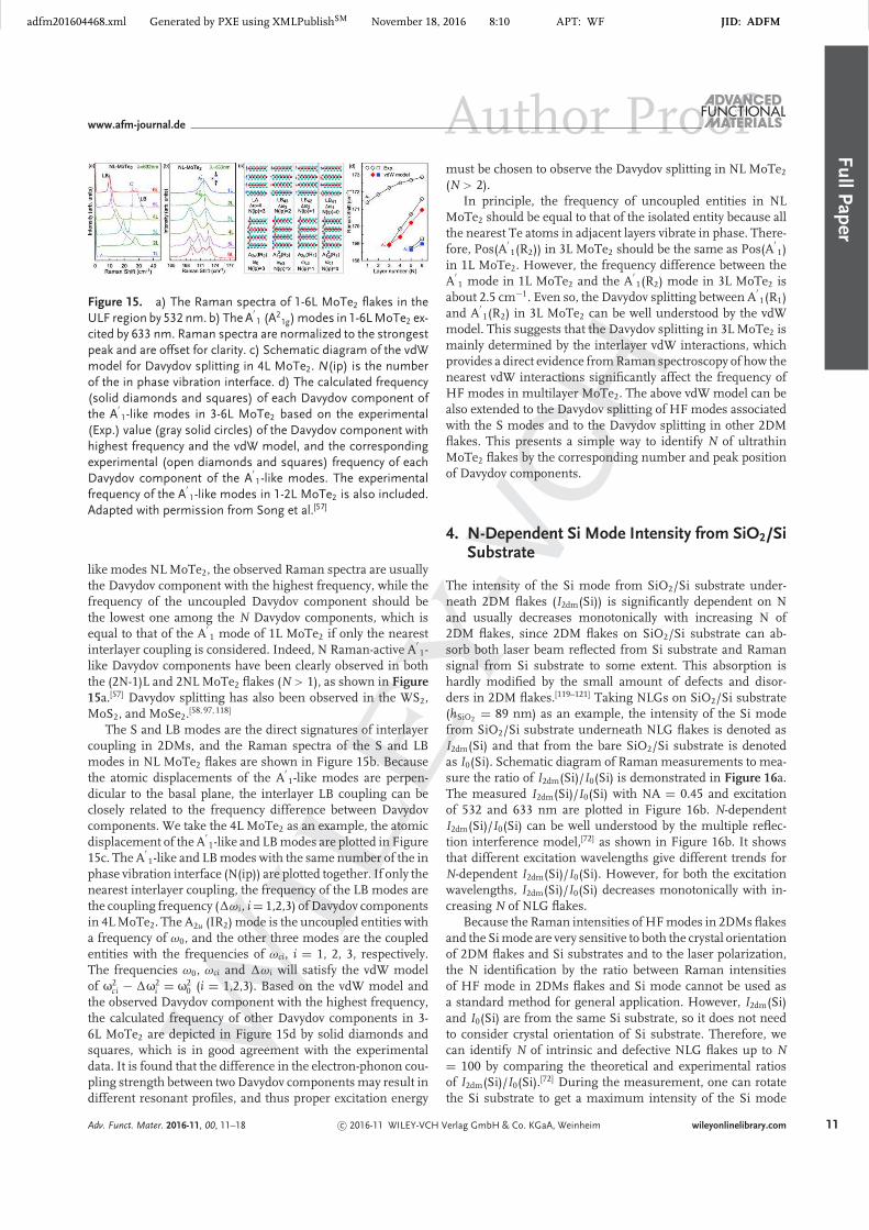
Figure 14. a) Raman spectrum of bulk Mo0.5W0.5S2 alloy in320–450 cm−1 ranges. b) Low-frequency Raman spectra of 2LMo0.5W0.5S2. The C mode is observable under both VV andHV configuration, while the LB mode is observable only underthe VV configuration. Raman spectra of c) C phonon branchesunder the HV configuration and d) LB phonon branches underthe VV-HV configuration in 2-11L Mo0.5W0.5S2. The theoretical(crosses) and experimental (squares) frequencies of e) C and f)LB modes in 2-11L Mo0.5W0.5S2. Adapted with permission fromQiao et al.[19]
3.3. Davydov Splitting
The frequency of HF modes in NL MX2 flakes should be de-pendent on the interlayer coupling between adjacent layers, i.e.,the coupling between two nearest X atoms in adjacent layersif only the nearest coupling is considered.[57] Once the nearestX atoms in adjacent layers vibrate out of phase, the additionalvdW interaction between the nearest X atoms in adjacent lay-ers will raise the frequency of the Raman mode with respectto the mode whose nearest X atoms in adjacent layers vibratein phase, leading to Davydov splitting.[57] Considering that twoidentical coupled entities have vibrational frequencies given byω0 and ωc, where ω0 is the frequency of the isolated entity andthat of two uncoupled entities when the two entities vibrate inphase, and ωc is the frequency of two coupled entities in whichthey vibrate out of phase, if 1ω is the coupling frequency be-tween two coupled entities, the three frequencies have the rela-tion of T2
c = T20 + 1�2.[116] 2L MX2 can exhibit clear signature
of the Davydov splitting as the case the S modes in twisted(2+2)LG.[42, 117] However, only one of the two Davydov com-ponents is usually Raman active, and it is difficult to directlyobserve Davydov splitting in 2L MX2.
We take the A′1 mode in 1L MoTe2 as an example to discuss
how the LB vibrations significantly affect the frequency of theHF A
′1-like modes in multilayer MoTe2. The A
′1 mode in 1L
MoTe2 will split into N A′1-like modes in NL MoTe2 (N >
1). These modes can be expressed as N+12
A′1+ N−1
2A
′ ′2 for ONL
MoTe2 and N2
A2u+ N2
A21g for ENL MoTe2 ,[10, 57, 93] where the A
′1
and A21g modes are Raman active and the A
′ ′2 and A2u modes
are infrared active. Therefore, for ONL MoTe2, it is expected toobserve (N+1)/2 Davydov components of A
′1-like mode, and
N/2 Davydov components of A′1 mode would be observed in
ENL MoTe2 in the corresponding Raman spectra. For the A′1-
10 wileyonlinelibrary.com c© 2016-11 WILEY-VCH Verlag GmbH & Co. KGaA, Weinheim Adv. Funct. Mater. 2016-11, 00, 10–18
adfm201604468.xml Generated by PXE using XMLPublishSM November 18, 2016 8:10 APT: WF JID: ADFMF
ullP
aper
Author Proofwww.afm-journal.de
Figure 15. a) The Raman spectra of 1-6L MoTe2 flakes in theULF region by 532 nm. b) The A
′1 (A2
1g) modes in 1-6L MoTe2 ex-cited by 633 nm. Raman spectra are normalized to the strongestpeak and are offset for clarity. c) Schematic diagram of the vdWmodel for Davydov splitting in 4L MoTe2. N(ip) is the numberof the in phase vibration interface. d) The calculated frequency(solid diamonds and squares) of each Davydov component ofthe A
′1-like modes in 3-6L MoTe2 based on the experimental
(Exp.) value (gray solid circles) of the Davydov component withhighest frequency and the vdW model, and the correspondingexperimental (open diamonds and squares) frequency of eachDavydov component of the A
′1-like modes. The experimental
frequency of the A′1-like modes in 1-2L MoTe2 is also included.
Adapted with permission from Song et al.[57]
like modes NL MoTe2, the observed Raman spectra are usuallythe Davydov component with the highest frequency, while thefrequency of the uncoupled Davydov component should bethe lowest one among the N Davydov components, which isequal to that of the A
′1 mode of 1L MoTe2 if only the nearest
interlayer coupling is considered. Indeed, N Raman-active A′1-
like Davydov components have been clearly observed in boththe (2N-1)L and 2NL MoTe2 flakes (N > 1), as shown in Figure15a.[57] Davydov splitting has also been observed in the WS2,MoS2, and MoSe2.[58, 97, 118]
The S and LB modes are the direct signatures of interlayercoupling in 2DMs, and the Raman spectra of the S and LBmodes in NL MoTe2 flakes are shown in Figure 15b. Becausethe atomic displacements of the A
′1-like modes are perpen-
dicular to the basal plane, the interlayer LB coupling can beclosely related to the frequency difference between Davydovcomponents. We take the 4L MoTe2 as an example, the atomicdisplacement of the A
′1-like and LB modes are plotted in Figure
15c. The A′1-like and LB modes with the same number of the in
phase vibration interface (N(ip)) are plotted together. If only thenearest interlayer coupling, the frequency of the LB modes arethe coupling frequency (1ωi, i = 1,2,3) of Davydov componentsin 4L MoTe2. The A2u (IR2) mode is the uncoupled entities witha frequency of ω0, and the other three modes are the coupledentities with the frequencies of ωci, i = 1, 2, 3, respectively.The frequencies ω0, ωci and 1ωi will satisfy the vdW modelof T2
ci − 1T2i = T2
0 (i = 1,2,3). Based on the vdW model andthe observed Davydov component with the highest frequency,the calculated frequency of other Davydov components in 3-6L MoTe2 are depicted in Figure 15d by solid diamonds andsquares, which is in good agreement with the experimentaldata. It is found that the difference in the electron-phonon cou-pling strength between two Davydov components may result indifferent resonant profiles, and thus proper excitation energy
must be chosen to observe the Davydov splitting in NL MoTe2
(N > 2).In principle, the frequency of uncoupled entities in NL
MoTe2 should be equal to that of the isolated entity because allthe nearest Te atoms in adjacent layers vibrate in phase. There-fore, Pos(A
′1(R2)) in 3L MoTe2 should be the same as Pos(A
′1)
in 1L MoTe2. However, the frequency difference between theA
′1 mode in 1L MoTe2 and the A
′1(R2) mode in 3L MoTe2 is
about 2.5 cm−1. Even so, the Davydov splitting between A′1(R1)
and A′1(R2) in 3L MoTe2 can be well understood by the vdW
model. This suggests that the Davydov splitting in 3L MoTe2 ismainly determined by the interlayer vdW interactions, whichprovides a direct evidence from Raman spectroscopy of how thenearest vdW interactions significantly affect the frequency ofHF modes in multilayer MoTe2. The above vdW model can bealso extended to the Davydov splitting of HF modes associatedwith the S modes and to the Davydov splitting in other 2DMflakes. This presents a simple way to identify N of ultrathinMoTe2 flakes by the corresponding number and peak positionof Davydov components.
4. N-Dependent Si Mode Intensity from SiO2/SiSubstrate
The intensity of the Si mode from SiO2/Si substrate under-neath 2DM flakes (I2dm(Si)) is significantly dependent on Nand usually decreases monotonically with increasing N of2DM flakes, since 2DM flakes on SiO2/Si substrate can ab-sorb both laser beam reflected from Si substrate and Ramansignal from Si substrate to some extent. This absorption ishardly modified by the small amount of defects and disor-ders in 2DM flakes.[119–121] Taking NLGs on SiO2/Si substrate(hSiO2
= 89 nm) as an example, the intensity of the Si modefrom SiO2/Si substrate underneath NLG flakes is denoted asI2dm(Si) and that from the bare SiO2/Si substrate is denotedas I0(Si). Schematic diagram of Raman measurements to mea-sure the ratio of I2dm(Si)/I0(Si) is demonstrated in Figure 16a.The measured I2dm(Si)/I0(Si) with NA = 0.45 and excitationof 532 and 633 nm are plotted in Figure 16b. N-dependentI2dm(Si)/I0(Si) can be well understood by the multiple reflec-tion interference model,[72] as shown in Figure 16b. It showsthat different excitation wavelengths give different trends forN-dependent I2dm(Si)/I0(Si). However, for both the excitationwavelengths, I2dm(Si)/I0(Si) decreases monotonically with in-creasing N of NLG flakes.
Because the Raman intensities of HF modes in 2DMs flakesand the Si mode are very sensitive to both the crystal orientationof 2DM flakes and Si substrates and to the laser polarization,the N identification by the ratio between Raman intensitiesof HF mode in 2DMs flakes and Si mode cannot be used asa standard method for general application. However, I2dm(Si)and I0(Si) are from the same Si substrate, so it does not needto consider crystal orientation of Si substrate. Therefore, wecan identify N of intrinsic and defective NLG flakes up to N= 100 by comparing the theoretical and experimental ratiosof I2dm(Si)/I0(Si).[72] During the measurement, one can rotatethe Si substrate to get a maximum intensity of the Si mode
Adv. Funct. Mater. 2016-11, 00, 11–18 c© 2016-11 WILEY-VCH Verlag GmbH & Co. KGaA, Weinheim wileyonlinelibrary.com 11
adfm201604468.xml Generated by PXE using XMLPublishSM November 18, 2016 8:10 APT: WF JID: ADFMF
ull
Pap
er
Author Proofwww.afm-journal.de
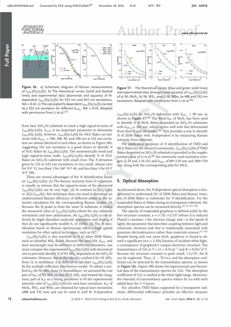
Figure 16. a) Schematic diagram of Raman measurementsof I2dm(Si)/I0(Si). b) The theoretical curves (solid and dashedlines) and experimental data (diamonds and squares) of N-dependent I2dm(Si)/I0(Si) for 532 nm and 633 nm excitations,NA = 0.45. c) The calculated N-dependent I2dm(Si)/I0(Si) excitedby a 532 nm excitation for different hSiO2
. NA = 0.45. Adaptedwith permission from Li et al.[72]
from bare SiO2/Si substrate to reach a high signal-to-noise ofI2dm(Si)/I0(Si). hSiO2 is an important parameter to determineI2dm(Si)/I0(Si), however, I2dm(Si)/I0(Si) for NLG flakes on sub-strate with hSiO2
= 290, 300, 90, and 100 nm at 532 nm excita-tion are almost identical to each other, as shown in Figure 16b,suggesting 532 nm excitation is a good choice to identify Nof NLG flakes by I2dm(Si)/I0(Si). The monotonically trend andhigh signal-to-noise make I2dm(Si)/I0(Si) identify N of NLGflakes on SiO2/Si substrate with small error. The N deviationgiven by 532 or 633 nm excitations is very small, almost zerofor N 2 15, less than 1 for 162 N 2 40, and less than 3 for 41 2N 2 100.
There are several advantages of the N identification basedon I2dm(Si)/I0(Si): (1) The Raman intensity from Si substratesis usually so intense that the signal-to-noise of the measuredI2dm(Si)/I0(Si) can be very high. (2) In contrast to I(G)/I0(Si)or I(G)/I2dm(Si), this technique does not need to introduce anundetermined Raman efficiency of different atoms in the in-tensity calculation for the corresponding Raman modes. (3)Because the Si peaks is from the same Si substrate, it makesthe measured value of I2dm(Si)/I0(Si) robust for any substrateorientation and laser polarization. (4) I2dm(Si)/I0(Si) is not af-fected by slight disorders molecule adsorption and doping ifthey do not significantly modify n8 of 2DMs. (5) The N iden-tification based on Raman spectroscopy offers a high spatialresolution for other optical techniques, such as OC.
I2dm(Si)/I0(Si) is also sensitive to N of other 2DM flakes,such as ultrathin MX2 flakes. Because the used NA, hSiO2
andlaser wavelength may be different in different laboratory, onemust compare the experimental I2dm(Si)/I0(Si) with theoreticalone to precisely identify N of NL MX2 deposited on the SiO2/Sisubstrates. However, due to the lake of a unified n for NL MX2
from 1L to multilayer, it is difficult to calculate I2dm(Si)/I0(Si)by the multiple reflection interference model. To obtain a uni-fied neff for NL MX2 from 1L to multilayer, we assumed the realpart of neff of NL MX2 as that of 1L MX2 and treated the imag-inary part of neff as a fitting parameter to fit the experimentalintensity ratio of I2dm(Si)/I0(Si) for each laser excitation. neff ofMoS2, WS2, and WSe2 are obtained for typical laser excitations(488 and 532 nm) and can be used to well fit N-dependent
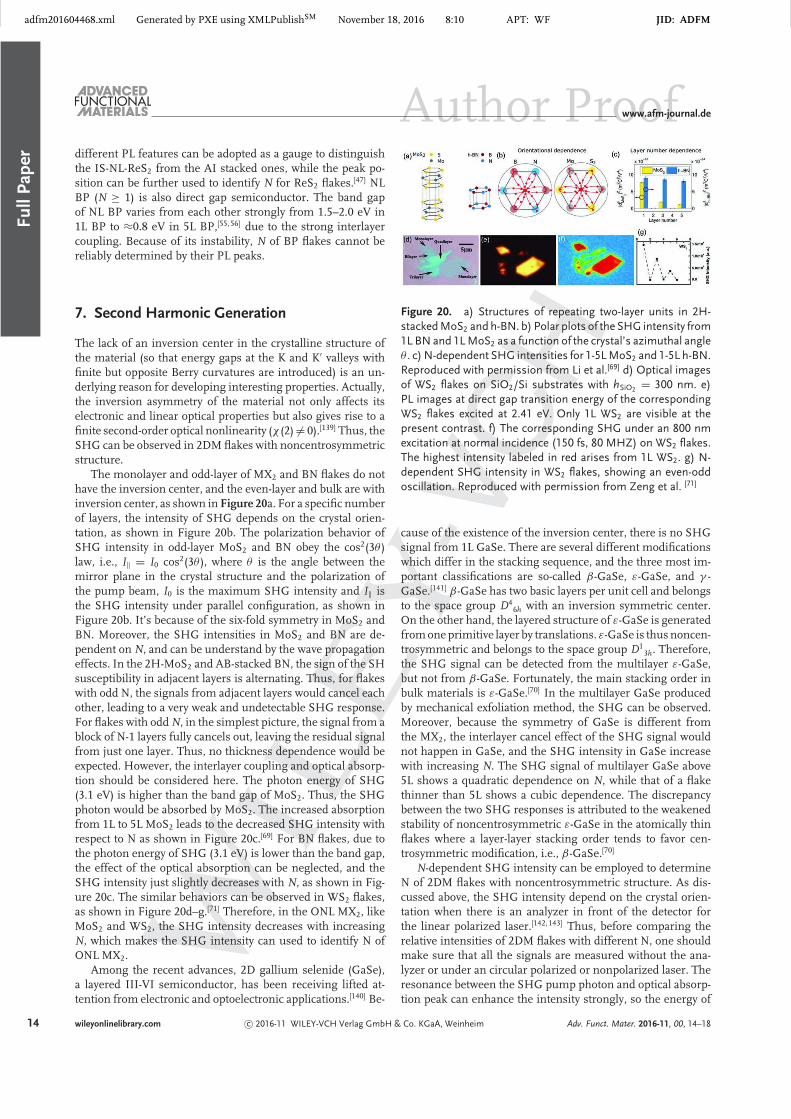
Figure 17. The theoretical curves (blue and green solid lines)and experimental data (triangles and squares) of I2dm(Si)/I0(Si)of a) NL MoS2, b) NL WS2, and c) NL WSe2 by 488 and 532 nmexcitations. Adapted with permission from Li et al.[86]
I2dm(Si)/I0(Si) for SiO2/Si substrates with hSiO2≃ 90 nm, as
shown in Figure 17.[86] The fitted neff of MoS2 has been usedto identify N of MoS2 flakes deposited on SiO2/Si substrateswith hSiO2
= 302 nm, which agrees well with that determinedfrom their S and LB modes.[86] This provides a way to identifyN of 2DM flakes with N-dependent n by measuring Ramanintensity from substrate.
For application purposes of N identification of TMD andMLG flakes for the research community, I2dm(Si)/I0(Si) of TMDflakes deposited on SiO2/Si substrate is provided in the supple-mentary data of Li et al.[86] for commonly used excitation ener-gies (2.34 and 2.54 eV) and hSiO2
of 80≈110 nm and 280≈310nm, along with the corresponding data for MLG.
5. Optical Absorption
As discussed above, the N-dependent optical absorption is fun-damental to understand OC of 2DM flakes and Raman inten-sity of 2DM flakes or substrates for N identification. For thesuspended flakes or flakes laying on transparent substrate, theabsorption spectra can be measured directly.[37, 53, 123–126]
The opacity of suspended graphene is defined solely by thefine structure constant, a = e2/ℏc ≈1/137 (where ℏ is reducedPlanck’s constant, e the electron charge and c is the speed oflight), the parameter that describes coupling between light andrelativistic electrons and that is traditionally associated withquantum electrodynamics rather than materials science.[37, 124]
Despite being only one atom thick, graphene is found to ab-sorb a significant (πa = 2.3%) fraction of incident white light,a consequence of graphene’s unique electronic structure. Thetransmittance of 1LG is T = (1 + 0.5πa)−2 and R = 0.25π 2a2T.Because the structure constant is quite small, ≈1/137, the Rcan be neglected. Thus, (1 − T)≈πa, and the absorption coef-ficient can be detected by the transmittance spectra, as shownin Figure 18a. Figure 18b shows the experimental and theoret-ical data of the transmittance spectra for 1LG. The absorptioncoefficient of 1LG is unified at the white light range. Moreover,the intensity of transmittance spectra reduce by πa with eachadded layer for 1–5 layers.
For ultrathin TMD flakes supported by a transparent sub-strate, differential reflectance provides an effective measure
12 wileyonlinelibrary.com c© 2016-11 WILEY-VCH Verlag GmbH & Co. KGaA, Weinheim Adv. Funct. Mater. 2016-11, 00, 12–18

adfm201604468.xml Generated by PXE using XMLPublishSM November 18, 2016 8:10 APT: WF JID: ADFMF
ullP
aper
Author Proofwww.afm-journal.de
Figure 18. a) Photograph of a 50 µm aperture partially cov-ered by 1LG and 2LG. The line scan profile shows the inten-sity of transmitted white light along the yellow line (Inset).The sample design: A 20 µm thick metal support structurehas several apertures of 20, 30, and 50 µm in diameter withgraphene crystallites placed over them. b) Transmittance spec-trum of 1LG (open circles). The red line is the transmittance T =(1+0.5πa)−2 expected for 2D Dirac fermions, whereas the greencurve takes into account a nonlinearity and triangular warpingof graphene’s electronic spectrum. The gray area indicates thestandard error for the measurements. (Inset) Transmittanceof white light as a function of the number of graphene layers(squares). The dashed lines correspond to an intensity reduc-tion by πa with each added layer. Reproduced with permissionfrom Nair et al.[37] Differential reflectance spectra of mechani-cally exfoliated c) 2H-WS2 and d) 2H-WSe2 flakes consisting of1–5 layers. The peaks are labeled according to the conventionproposed by Wilson and Yoffe.[122] Reproduced with permissionfrom Zhao et al.[53]
of absorbance.[53, 69, 125, 126] The fractional change in reflectanceδR for a thin layer sample relative to the reflectance of a di-electric substrate with refractive index of nsubs is related to theabsorbance (A) of the material by: *R(8) = 4
n2subs
−1A(8).[127] nsubs
can be assumed as wavelength independent for the visible spec-tral range on the quartz substrate. All peaks exhibit a gradualbut distinct blueshift with decreasing flake thickness.[53] N-dependent absorption can also be expected in other 2DMs,such as BP, ReS2 and InSe.[128–130]
Because the absorbance of 2DM flakes usually increaseswith increasing N, the transmittance spectra (absorption spec-tra) can be used to identify the N of 2DM flakes, such as MLGsand TMDs. However, due to the measurement requirement ofabsorption spectra, it just is suitable to identify the N of 2DMflakes that are suspended or on transparent substrate.
Figure 19. PL spectrum of a) 1-6L MoS2 and b) 1-6L WS2,where the lowest-energy peak is labeled by arrow. The lowesttransition energies in c) NL MoS2 and d) NL WS2 as a functionof N.
6. Photoluminescence
Most MX2 are indirect gap semiconductors in bulk, but trans-form to direct gap semiconductors when thickness is reducedto monolayer.[33, 34, 53] The indirect-to-direct transition is at-tributed to the absence of weak interlayer coupling in themonolayer,[33, 34, 131] which was directly verified in NL MoSe2 viainterlayer thermal expansion. An excited electron will attract ahole by Coulomb interactions to form a bound state (called anexciton) with the bound energy levels lying in the band-gapregion. This excitonic effect is significantly enhanced in 2DMsowing to strong spatial confinement and a reduced screeningeffect.[132–135] Thus, as a 2DM, 1L MX2 is expected to have astrong excitonic effect with a large exciton binding energy of0.5-1.0 eV,[136–138] which will significantly influence its opticalproperties, e.g., PL and optical absorption.
The indirect-to-direct band-gap transition from bulk to 1LMoS2 (also WS2, WSe2, and MoSe2) leads to enhanced PL emis-sion in 1L MoS2 and decrease in PL intensity with increasingN. For 2-6L MoS2 and some of other MX2 flakes, the indirectband gap (lowest PL peak position) decreases with increasingN. Figure 19a,b show PL spectra of 1-6L MoS2 and 1-6L WS2,respectively. The PL spectrum of 1L MoS2 and 1L WS2 con-sists of a single narrow feature due to their direct band-gapstructure, which make them be easily distinguished from theirmultilayer. In contrast, there are multiple emission peaks in2-6L MoS2 and 2-6L WS2, where the lowest-energy peak (la-beled as I) shifts to lower energies with increasing N due to theindirect band-gap structure changing with N. The transitionsof NL MoS2 and WS2 with lowest energies are summarizedin Figure 19c,d. Therefore, the lowest transition energy in PLspectra can be used to identify N of NL MoS2 and NL WS2
when N<6. This technique can also be applied to other MX2
flakes, such as WSe2, MoSe2 and MoTe2.The N-dependent PL spectra have also been measured from
other semiconducting 2DM flakes, such as ReS2, ReSe2, andBP.[47, 55, 56, 107] 1L ReS2 and both AI- and IS-NL-ReS2 are directband-gap semiconductors. The PL profile of AI-NL-ReS2 is sim-ilar to that of 1L ReS2. However, the PL profile of IS-NL-ReS2 isnarrower and shows a sharper peak at the peak center. These
Adv. Funct. Mater. 2016-11, 00, 13–18 c© 2016-11 WILEY-VCH Verlag GmbH & Co. KGaA, Weinheim wileyonlinelibrary.com 13
adfm201604468.xml Generated by PXE using XMLPublishSM November 18, 2016 8:10 APT: WF JID: ADFMF
ull
Pap
er
Author Proofwww.afm-journal.de
different PL features can be adopted as a gauge to distinguishthe IS-NL-ReS2 from the AI stacked ones, while the peak po-sition can be further used to identify N for ReS2 flakes.[47] NLBP (N ≥ 1) is also direct gap semiconductor. The band gapof NL BP varies from each other strongly from 1.5–2.0 eV in1L BP to ≈0.8 eV in 5L BP,[55, 56] due to the strong interlayercoupling. Because of its instability, N of BP flakes cannot bereliably determined by their PL peaks.
7. Second Harmonic Generation
The lack of an inversion center in the crystalline structure ofthe material (so that energy gaps at the K and K′ valleys withfinite but opposite Berry curvatures are introduced) is an un-derlying reason for developing interesting properties. Actually,the inversion asymmetry of the material not only affects itselectronic and linear optical properties but also gives rise to afinite second-order optical nonlinearity (χ (2) 6= 0).[139] Thus, theSHG can be observed in 2DM flakes with noncentrosymmetricstructure.
The monolayer and odd-layer of MX2 and BN flakes do nothave the inversion center, and the even-layer and bulk are withinversion center, as shown in Figure 20a. For a specific numberof layers, the intensity of SHG depends on the crystal orien-tation, as shown in Figure 20b. The polarization behavior ofSHG intensity in odd-layer MoS2 and BN obey the cos2(3θ )law, i.e., I‖ = I0 cos2(3θ ), where θ is the angle between themirror plane in the crystal structure and the polarization ofthe pump beam, I0 is the maximum SHG intensity and I‖ isthe SHG intensity under parallel configuration, as shown inFigure 20b. It’s because of the six-fold symmetry in MoS2 andBN. Moreover, the SHG intensities in MoS2 and BN are de-pendent on N, and can be understand by the wave propagationeffects. In the 2H-MoS2 and AB-stacked BN, the sign of the SHsusceptibility in adjacent layers is alternating. Thus, for flakeswith odd N, the signals from adjacent layers would cancel eachother, leading to a very weak and undetectable SHG response.For flakes with odd N, in the simplest picture, the signal from ablock of N-1 layers fully cancels out, leaving the residual signalfrom just one layer. Thus, no thickness dependence would beexpected. However, the interlayer coupling and optical absorp-tion should be considered here. The photon energy of SHG(3.1 eV) is higher than the band gap of MoS2. Thus, the SHGphoton would be absorbed by MoS2. The increased absorptionfrom 1L to 5L MoS2 leads to the decreased SHG intensity withrespect to N as shown in Figure 20c.[69] For BN flakes, due tothe photon energy of SHG (3.1 eV) is lower than the band gap,the effect of the optical absorption can be neglected, and theSHG intensity just slightly decreases with N, as shown in Fig-ure 20c. The similar behaviors can be observed in WS2 flakes,as shown in Figure 20d–g.[71] Therefore, in the ONL MX2, likeMoS2 and WS2, the SHG intensity decreases with increasingN, which makes the SHG intensity can used to identify N ofONL MX2.
Among the recent advances, 2D gallium selenide (GaSe),a layered III-VI semiconductor, has been receiving lifted at-tention from electronic and optoelectronic applications.[140] Be-
Figure 20. a) Structures of repeating two-layer units in 2H-stacked MoS2 and h-BN. b) Polar plots of the SHG intensity from1L BN and 1L MoS2 as a function of the crystal’s azimuthal angleθ . c) N-dependent SHG intensities for 1-5L MoS2 and 1-5L h-BN.Reproduced with permission from Li et al.[69] d) Optical imagesof WS2 flakes on SiO2/Si substrates with hSiO2
= 300 nm. e)PL images at direct gap transition energy of the correspondingWS2 flakes excited at 2.41 eV. Only 1L WS2 are visible at thepresent contrast. f) The corresponding SHG under an 800 nmexcitation at normal incidence (150 fs, 80 MHZ) on WS2 flakes.The highest intensity labeled in red arises from 1L WS2. g) N-dependent SHG intensity in WS2 flakes, showing an even-oddoscillation. Reproduced with permission from Zeng et al. [71]
cause of the existence of the inversion center, there is no SHGsignal from 1L GaSe. There are several different modificationswhich differ in the stacking sequence, and the three most im-portant classifications are so-called β-GaSe, ε-GaSe, and γ -GaSe.[141] β-GaSe has two basic layers per unit cell and belongsto the space group D4
6h with an inversion symmetric center.On the other hand, the layered structure of ε-GaSe is generatedfrom one primitive layer by translations. ε-GaSe is thus noncen-trosymmetric and belongs to the space group D1
3h. Therefore,the SHG signal can be detected from the multilayer ε-GaSe,but not from β-GaSe. Fortunately, the main stacking order inbulk materials is ε-GaSe.[70] In the multilayer GaSe producedby mechanical exfoliation method, the SHG can be observed.Moreover, because the symmetry of GaSe is different fromthe MX2, the interlayer cancel effect of the SHG signal wouldnot happen in GaSe, and the SHG intensity in GaSe increasewith increasing N. The SHG signal of multilayer GaSe above5L shows a quadratic dependence on N, while that of a flakethinner than 5L shows a cubic dependence. The discrepancybetween the two SHG responses is attributed to the weakenedstability of noncentrosymmetric ε-GaSe in the atomically thinflakes where a layer-layer stacking order tends to favor cen-trosymmetric modification, i.e., β-GaSe.[70]
N-dependent SHG intensity can be employed to determineN of 2DM flakes with noncentrosymmetric structure. As dis-cussed above, the SHG intensity depend on the crystal orien-tation when there is an analyzer in front of the detector forthe linear polarized laser.[142, 143] Thus, before comparing therelative intensities of 2DM flakes with different N, one shouldmake sure that all the signals are measured without the ana-lyzer or under an circular polarized or nonpolarized laser. Theresonance between the SHG pump photon and optical absorp-tion peak can enhance the intensity strongly, so the energy of
14 wileyonlinelibrary.com c© 2016-11 WILEY-VCH Verlag GmbH & Co. KGaA, Weinheim Adv. Funct. Mater. 2016-11, 00, 14–18
adfm201604468.xml Generated by PXE using XMLPublishSM November 18, 2016 8:10 APT: WF JID: ADFMF
ullP
aper
Author Proofwww.afm-journal.de
the pump laser should be chosen carefully to be out of theresonant window.[144, 145]
8. Conclusions
The neighboring layers of layered LMs can easily slide againsteach other so that a single monolayer or multilayer can be fabri-cated by mechanical exfoliation to form atomically thin crystals,known as 2DMs. The properties of 2DMs are highly related totheir N. Here, we review the evolution of optical properties(e.g., OC, Rayleigh scattering, Raman spectroscopy, optical ab-sorption, PL and SHG) of several typical 2DMs from monolayerto multilayer when they are suspended or deposited on somekinds of substrates. The optical parameters of peak position,peak area (intensity) and linewidth are discussed in detail toreveal how to utilize these optical parameters to rapidly andaccurately determine N or thickness of the 2DM flakes in theirown applicable scope, which is essential to their fundamen-tal studies and practical applications. These optical techniquesalso have own disadvantages in terms of determining N of2DM flakes and may cause ambiguity for providing reliableinformation if they are not utilized properly. In this case, forsome specific 2DM flakes, the combination of two or more op-tical techniques are necessary to accurately determine their Nor thickness.
There are now reported to be several hundred companiesworldwide producing or using graphene and other 2DMs.Many issues must be concerned to face the large-scale produc-tion, processing and application of 2DMs when one considerthe world outside of the laboratory. For industry to have confi-dence in graphene materials produced commercially, the prop-erties of these materials must be accurately, reliably and repro-ducibly measured. The properties of 2DMs are highly relatedto their thickness, i.e., layer number (N), and thus the N deter-mination of 2DM flakes is critical to cater to quality appraisalsfor the 2DM industrial products. Therefore, standardization onthe N determination of 2DM flakes will be crucial to allow thecomparison of flake thickness for many different 2DMs pro-duced worldwide, as well as for comparisons against differenttechnologies. This review demonstrates that these optical tech-niques can be expected to service as robust, fast, accurate, non-destructive and even substrate-free approaches for N countingor thickness identification of 2DM flakes produced by micro-mechanical exfoliations, chemical-vapor-deposition growth, ortransfer processes on various substrates, which bridges the gapbetween the characterization and international standardizationfor thickness determination of 2DM flakes and the gap betweenacademia and industry.
Supporting Information
Supporting Information is available from the Wiley OnlineLibrary or from the author.
Acknowledgements
X.-L.L., W.-P.H., and J.-B.W. contributed equally to thiswork. The authors acknowledge support from National Ba-sic Research Program of China (Grant No. 2016YFA0301200),National Natural Science Foundation of China (GrantNos. 11225421, 11434010, 11474277, 11504077, 11574305,51527901, 11604173), Natural Science Foundation of Shan-dong Province in China (Grant No. BS2015CL013), Programof Science and Technology in Qingdao City (Grant No. 15-9-1-112-jch) and National Young 1000 Talent Plan of China.
Received: August 29, 2016Revised: October 24, 2016
Published Online: MM DD, YYYY
[1] K. Novoselov, D. Jiang, F. Schedin, T. Booth, V. Khotkevich,
S. Morozov, A. Geim, Proc. Natl. Acad. Sci. USA 2005, 102,
10451.
[2] J. N. Coleman, M. Lotya, A. O’Neill, S. D. Bergin, P. J. King, U.
Khan, K. Young, A. Gaucher, S. De, R. J. Smith, I. V. Shvets,
S. K. Arora, G. Stanton, H. Y. Kim, K. Lee, G. T. Kim, G. S.
Duesberg, T. Hallam, J. J. Boland, J. J. Wang, J. F. Donegan,
J. C. Grunlan, G. Moriarty, A. Shmeliov, R. J. Nicholls, J. M.
Perkins, E. M. Grieveson, K. Theuwissen, D. W. McComb, P.
D. Nellist, V. Nicolosi, Science 2011, 331, 568.
[3] X. Zhang, Q.-H. Tan, J.-B. Wu, W. Shi, P.-H. Tan, Nanoscale
2016, 8, 6435.
[4] R. V. Gorbachev, I. Riaz, R. R. Nair, R. Jalil, L. Britnell, B. D.
Belle, E. W. Hill, K. S. Novoselov, K. Watanabe, T. Taniguchi,
A. K. Geim, P. Blake, Small 2011, 7, 465.
[5] K. Xu, Z. Wang, F. Wang, Y. Huang, F. Wang, L. Yin, C. Jiang,
J. He, Adv. Mater. 2015, 27, 7881.
[6] D. S. Kong, W. H. Dang, J. J. Cha, H. Li, S. Meister, H. L.
Peng, Z. F. Liu, Y. Cui, Nano Lett. 2010, 10, 2245.
[7] J. Zhang, Z. Peng, A. Soni, Y. Zhao, Y. Xiong, B. Peng, J.
Wang, M. S. Dresselhaus, Q. Xiong, Nano Lett. 2011, 11, 2407.
[8] Q. H. Wang, K. Kalantar-Zadeh, A. Kis, J. N. Coleman, M. S.
Strano, Nat. Nanotechnol. 2012, 7, 699.
[9] M. Chhowalla, H. S. Shin, G. Eda, L. J. Li, K. P. Loh, H. Zhang,
Nat. Chem. 2013, 5, 263.
[10] X. Zhang, X. F. Qiao, W. Shi, J. B. Wu, D. S. Jiang, P. H. Tan,
Chem. Soc. Rev. 2015, 44, 2757.
[11] D. J. Late, B. Liu, H. S. S. R. Matte, C. N. R. Rao, V. P. Dravid,
Adv. Funct. Mater. 2012, 22, 1894.
[12] W. Feng, J.-B. Wu, X. Li, W. Zheng, X. Zhou, K. Xiao, W.
Cao, B. Yang, J.-C. Idrobo, L. Basile, W. Tian, P. Tan, P. Hu,
J. Mater. Chem. C 2015, 3, 7022.
[13] K. S. Novoselov, A. K. Geim, S. V. Morozov, D. Jiang, Y.
Zhang, S. V. Dubonos, I. V. Grigorieva, A. A. Firsov, Science
2004, 306, 666.
[14] M. N. Ali, J. Xiong, S. Flynn, J. Tao, Q. D. Gibson, L. M.
Schoop, T. Liang, N. Haldolaarachchige, M. Hirschberger, N.
P. Ong, R. J. Cava, Nature 2014, 514, 205.
[15] Q. Song, X. Pan, H. Wang, K. Zhang, Q. Tan, P. Li, Y. Wan,
Y. Wang, X. Xu, M. Lin, X. Wan, F. Song, L. Dai, Sci. Rep.
2016, 6, 29254.
[16] K. S. Novoselov, A. H. Castro Neto, Phys. Scr. 2012, T146,
014006.
[17] F. Xia, H. Wang, Y. Jia, Nat. Commun. 2014, 5, 4458.
[18] L. Li, Y. Yu, G. J. Ye, Q. Ge, X. Ou, H. Wu, D. Feng, X. H.
Chen, Y. Zhang, Nat. Nanotechnol. 2014, 9, 372.
Adv. Funct. Mater. 2016-11, 00, 15–18 c© 2016-11 WILEY-VCH Verlag GmbH & Co. KGaA, Weinheim wileyonlinelibrary.com 15
adfm201604468.xml Generated by PXE using XMLPublishSM November 18, 2016 8:10 APT: WF JID: ADFMF
ull
Pap
er
Author Proofwww.afm-journal.de
[19] X. F. Qiao, X. L. Li, X. Zhang, W. Shi, J. B. Wu, T. Chen, P. H.
Tan, Appl. Phys. Lett. 2015, 106, 223102.
[20] C. Xia, J. Li, J. Semicond. 2016, 37, 051001.
[21] Z. Lou, Z. Liang, G. Shen, J. Semicond. 2016, 37, 091001.
[22] L. Tao, D. Wang, S. Jiang, Y. Liu, Q. Xie, H. Tian, N. Deng,
X. Wang, Y. Yang, T. Ren, J. Semicond. 2016, 37, 041001.
[23] X. S. Li, Y. W. Zhu, W. W. Cai, M. Borysiak, B. Y. Han, D.
Chen, R. D. Piner, L. Colombo, R. S. Ruoff, Nano Lett. 2009,
9, 4359.
[24] Y. Sui, J. Appenzeller, Nano Lett. 2009, 9, 2973.
[25] Y. M. Lin, C. Dimitrakopoulos, K. A. Jenkins, D. B. Farmer, H.
Y. Chiu, A. Grill, P. Avouris, Science 2010, 327, 662.
[26] B. Radisavljevic, A. Radenovic, J. Brivio, V. Giacometti, A. Kis,
Nat. Nanotechnol. 2011, 6, 147.
[27] Y. W. Zhu, S. Murali, M. D. Stoller, K. J. Ganesh, W. W. Cai,
P. J. Ferreira, A. Pirkle, R. M. Wallace, K. A. Cychosz, M.
Thommes, D. Su, E. A. Stach, R. S. Ruoff, Science 2011, 332,
1537.
[28] D. Xiao, G. B. Liu, W. X. Feng, X. D. Xu, W. Yao, Phys. Rev.
Lett. 2012, 108, 196802.
[29] S. Kim, A. Konar, W. S. Hwang, J. H. Lee, J. Lee, J. Yang,
C. Jung, H. Kim, J. B. Yoo, J. Y. Choi, Y. W. Jin, S. Y. Lee, D.
Jena, W. Choi, K. Kim, Nat. Commun. 2012, 3, 1011.
[30] F. Xia, H. Wang, D. Xiao, M. Dubey, A. Ramasubramaniam,
Nat. Photonics 2014, 8, 899.
[31] E. F. Liu, Y. J. Fu, Y. J. Wang, Y. Q. Feng, H. M. Liu, X. G.
Wan, W. Zhou, B. G. Wang, L. B. Shao, C. H. Ho, Y. S. Huang,
Z. Y. Cao, L. G. Wang, A. D. Li, J. W. Zeng, F. Q. Song, X. R.
Wang, Y. Shi, H. T. Yuan, H. Y. Hwang, Y. Cui, F. Miao, D. Y.
Xing, Nat. Commun. 2015, 6, 6991.
[32] K. S. Novoselov, A. K. Geim, S. V. Morozov, D. Jiang, M.
I. Katsnelson, I. V. Grigorieva, S. V. Dubonos, A. A. Firsov,
Nature 2005, 438, 197.
[33] K. F. Mak, C. Lee, J. Hone, J. Shan, T. F. Heinz, Phys. Rev.
Lett. 2010, 105, 136805.
[34] A. Splendiani, L. Sun, Y. Zhang, T. Li, J. Kim, C.-Y. Chim, G.
Galli, F. Wang, Nano Lett. 2010, 10, 1271.
[35] A. A. Balandin, S. Ghosh, W. Z. Bao, I. Calizo, D. Tewelde-
brhan, F. Miao, C. N. Lau, Nano Lett. 2008, 8, 902.
[36] C. Lee, X. D. Wei, J. W. Kysar, J. Hone, Science 2008, 321, 385.
[37] R. R. Nair, P. Blake, A. N. Grigorenko, K. S. Novoselov, T. J.
Booth, T. Stauber, N. M. R. Peres, A. K. Geim, Science 2008,
320, 1308.
[38] A. K. Geim, K. S. Novoselov, Nat. Mater. 2007, 6, 183.
[39] M. S. Xu, T. Liang, M. M. Shi, H. Z. Chen, Chem. Rev. 2013,
113, 3766.
[40] C. H. Lui, Z. Li, Z. Chen, P. V. Klimov, L. E. Brus, T. F. Heinz,
Nano Lett. 2010, 11, 164.
[41] C. Cong, T. Yu, K. Sato, J. Shang, R. Saito, G. F. Dresselhaus,
M. S. Dresselhaus, ACS Nano 2011, 5, 8760.
[42] J. B. Wu, X. Zhang, M. Ijäs, W. P. Han, X. F. Qiao, X. L. Li,
D. S. Jiang, A. C. Ferrari, P. H. Tan, Nat. Commun. 2014, 5,
5309.
[43] J. B. Wu, Z. X. Hu, X. Zhang, W. P. Han, Y. Lu, W. Shi, X. F.
Qiao, M. Ijias, S. Milana, W. Ji, A. C. Ferrari, P. H. Tan, ACS
Nano 2015, 9, 7440.
[44] X. Lu, M. Utama, J. Lin, X. Luo, Y. Zhao, J. Zhang, S. T.
Pantelides, W. Zhou, S. Y. Quek, Q. Xiong, Adv. Mater. 2015,
27, 4502.
[45] X. Luo, X. Lu, C. Cong, T. Yu, Q. Xiong, S. Y. Quek, Sci. Rep.
2015, 5, 14565.
[46] A. A. Puretzky, L. Liang, X. Li, K. Xiao, K. Wang, M. Mahjouri-
Samani, L. Basile, J. C. Idrobo, B. G. Sumpter, V. Meunier, D.
B. Geohegan, ACS Nano 2015, 9, 6333.
[47] X. F. Qiao, J. B. Wu, L. W. Zhou, J. S. Qiao, W. Shi, T. Chen,
X. Zhang, J. Zhang, W. Ji, P. H. Tan, Nanoscale 2016, 8, 8324.
[48] A. K. Geim, I. V. Grigorieva, Nature 2013, 499, 419.
[49] H. Fang, C. Battaglia, C. Carraro, S. Nemsak, B. Ozdol, J. S.
Kang, H. A. Bechtel, S. B. Desai, F. Kronast, A. A. Unal, G.
Conti, C. Conlon, G. K. Palsson, M. C. Martin, A. M. Minor,
C. S. Fadley, E. Yablonovitch, R. Maboudian, A. Javey, Proc.
Natl. Acad. Sci. USA 2014, 111, 6198.
[50] X. Wang, F. Xia, Nat. Mater. 2015, 14, 264.
[51] F. Withers, O. Del Pozo-Zamudio, A. Mishchenko, A. P.
Rooney, A. Gholinia, K. Watanabe, T. Taniguchi, S. J. Haigh,
A. K. Geim, A. I. Tartakovskii, K. S. Novoselov, Nat. Mater.
2015, 14, 301.
[52] B. Partoens, F. M. Peeters, Phys. Rev. B 2006, 74, 075404.
[53] W. J. Zhao, Z. Ghorannevis, L. Q. Chu, M. L. Toh, C. Kloc, P.
H. Tan, G. Eda, ACS Nano 2013, 7, 791.
[54] Y. L. Li, A. Chernikov, X. Zhang, A. Rigosi, H. M. Hill, A. M.
van der Zande, D. A. Chenet, E. M. Shih, J. Hone, T. F. Heinz,
Phys. Rev. B 2014, 90, 205422.
[55] S. Zhang, J. Yang, R. Xu, F. Wang, W. Li, M. Ghufran, Y.-W.
Zhang, Z. Yu, G. Zhang, Q. Qin, Y. Lu, ACS Nano 2014, 8,
9590.
[56] X. Wang, A. M. Jones, K. L. Seyler, V. Tran, Y. Jia, H. Zhao,
H. Wang, L. Yang, X. Xu, F. Xia, Nat. Nanotechnol. 2015, 10,
517.
[57] Q. J. Song, Q. H. Tan, X. Zhang, J. B. Wu, B. W. Sheng, Y.
Wan, X. Q. Wang, L. Dai, P. H. Tan, Phys. Rev. B 2016, 93,
115409.
[58] K. Kim, J.-U. Lee, D. Nam, H. Cheong, ACS Nano 2016, 10,
8113.
[59] A. Molina-Sanchez, L. Wirtz, Phys. Rev. B 2011, 84, 155413.
[60] P. Blake, E. W. Hill, A. H. C. Neto, K. S. Novoselov, D. Jiang,
R. Yang, T. J. Booth, A. K. Geim, Appl. Phys. Lett. 2007, 91,
063124.
[61] Z. H. Ni, H. M. Wang, J. Kasim, H. M. Fan, T. Yu, Y. H. Wu,
Y. P. Feng, Z. X. Shen, Nano Lett. 2007, 7, 2758.
[62] I. Jung, M. Pelton, R. Piner, D. A. Dikin, S. Stankovich, S.
Watcharotone, M. Hausner, R. S. Ruoff, Nano Lett. 2007, 7,
3569.
[63] H. Li, J. M. T. Wu, X. Huang, G. Lu, J. Yang, X. Lu, Q. H.
Zhang, H. Zhang, ACS Nano 2013, 7, 10344.
[64] C. Casiraghi, A. Hartschuh, E. Lidorikis, H. Qian, H. Haru-
tyunyan, T. Gokus, K. S. Novoselov, A. C. Ferrari, Nano Lett.
2007, 7, 2711.
[65] L. Malard, M. Pimenta, G. Dresselhaus, M. Dresselhaus, Phys.
Rep. 2009, 473, 51.
[66] A. C. Ferrari, J. C. Meyer, V. Scardaci, C. Casiraghi, M. Lazzeri,
F. Mauri, S. Piscanec, D. Jiang, K. S. Novoselov, S. Roth, A.
K. Geim, Phys. Rev. Lett. 2006, 97, 187401.
[67] P. H. Tan, W. P. Han, W. J. Zhao, Z. H. Wu, K. Chang, H.
Wang, Y. F. Wang, N. Bonini, N. Marzari, N. Pugno, G. Savini,
A. Lombardo, A. C. Ferrari, Nat. Mater. 2012, 11, 294.
[68] M. Bruna, S. Borini, Appl. Phys. Lett. 2009, 94, 031901.
[69] Y. Li, Y. Rao, K. F. Mak, Y. You, S. Wang, C. R. Dean, T. F.
Heinz, Nano Lett. 2013, 13, 3329.
[70] W. Jie, X. Chen, D. Li, L. Xie, Y. Y. Hui, S. P. Lau, X. Cui, J.
Hao, Angew. Chem., Int. Ed. 2015, 54, 1185.
[71] H. Zeng, G.-B. Liu, J. Dai, Y. Yan, B. Zhu, R. He, L. Xie, S.
Xu, X. Chen, W. Yao, X. Cui, Sci. Rep. 2013, 3, 1608.
[72] X. L. Li, X. F. Qiao, W. P. Han, Y. Lu, Q. H. Tan, X. L. Liu, P.
H. Tan, Nanoscale 2015, 7, 8135.
[73] Y. K. Koh, M. H. Bae, D. G. Cahill, E. Pop, ACS Nano 2011, 5,
269.
16 wileyonlinelibrary.com c© 2016-11 WILEY-VCH Verlag GmbH & Co. KGaA, Weinheim Adv. Funct. Mater. 2016-11, 00, 16–18

adfm201604468.xml Generated by PXE using XMLPublishSM November 18, 2016 8:10 APT: WF JID: ADFMF
ullP
aper
Author Proofwww.afm-journal.de
[74] V. G. Kravets, A. N. Grigorenko, R. R. Nair, P. Blake, S.
Anissimova, K. S. Novoselov, A. K. Geim, Phys. Rev. B 2010,
81, 155413.
[75] E. D. Palik, Handbook of Optical Constants of Solids, Academic
Press, New York, 1985.
[76] X. Qin, Y. Chen, Y. Liu, L. Zhu, Y. Li, Q. Wu, W. Huang, J.
Semicond. 2016, 37, 013002.
[77] N. Mao, J. Tang, L. Xie, J. Wu, B. Han, J. Lin, S. Deng, W. Ji,
H. Xu, K. Liu, L. Tong, J. Zhang, J. Am. Chem. Soc. 2015, 138,
300.
[78] J.-B. Wu, H. Zhao, Y. Li, D. Ohlberg, W. Shi, W. Wu, H.
Wang, P.-H. Tan, Adv. Opt. Mater. 2016, 4, 756.
[79] W. P. Han, Y. M. Shi, X. L. Li, S. Q. Luo, Y. Lu, P. H. Tan,
Acta Phys. Sin. 2013, 62, 110702.
[80] Y. Lu, X. L. Li, X. Zhang, J. B. Wu, P. H. Tan, Sci. Bull. 2015,
60, 806.
[81] D. Cole, J. Shallenberger, S. Novak, R. Moore, M. Edgell, S.
Smith, C. Hitzman, J. Kirchhoff, E. Principe, W. Nieveen, F.
Huang, S. Biswas, R. Bleiler, K. Jones, J. Vac. Sci. Technol., B
2000, 18, 440.
[82] J. W. Park, H. S. So, S. Kim, S. H. Choi, H. Lee, J. Lee, C. Lee,
Y. Kim, J. Appl. Phys. 2014, 116, 183509.
[83] J.-B. Wu, H. Wang, X.-L. Li, H. Peng, P.-H. Tan, Carbon 2016,
110, 225.
[84] A. C. Ferrari, D. M. Basko, Nat. Nanotechnol. 2013, 8, 235.
[85] X. Zhang, W. P. Han, J. B. Wu, S. Milana, Y. Lu, Q. Q. Li, A.
C. Ferrari, P. H. Tan, Phys. Rev. B 2013, 87, 115413.
[86] X. L. Li, X. F. Qiao, W. P. Han, X. Zhang, Q. H. Tan, T. Chen,
P. H. Tan, Nanotechnology 2016, 27, 145704.
[87] W. J. Zhao, P. H. Tan, J. Zhang, J. Liu, Phys. Rev. B 2010, 82,
245423.
[88] X. Zhang, W.-P. Han, X.-F. Qiao, Q.-H. Tan, Y.-F. Wang, J.
Zhang, P.-H. Tan, Carbon 2016, 99, 118.
[89] R. S. Sundaram, M. Engel, A. Lombardo, R. Krupke, A. C.
Ferrari, P. Avouris, M. Steiner, Nano Lett. 2013, 13, 1416.
[90] T. Cao, G. Wang, W. P. Han, H. Q. Ye, C. R. Zhu, J. R. Shi,
Q. Niu, P. H. Tan, E. Wang, B. L. Liu, J. Feng, Nat. Commun.
2012, 3, 887.
[91] H. L. Zeng, J. F. Dai, W. Yao, D. Xiao, X. D. Cui, Nat.
Nanotechnol. 2012, 7, 490.
[92] K. F. Mak, K. L. He, J. Shan, T. F. Heinz, Nat. Nanotechnol.
2012, 7, 494.
[93] G. Froehlicher, E. Lorchat, F. Fernique, C. Joshi, A. Molina-
Sanchez, L. Wirtz, S. Berciaud, Nano Lett. 2015, 15, 6481.
[94] C. Lee, H. Yan, L. E. Brus, T. F. Heinz, J. Hone, S. Ryu, ACS
Nano 2010, 4, 2695.
[95] H. Li, Q. Zhang, C. C. R. Yap, B. K. Tay, T. H. T. Edwin, A.
Olivier, D. Baillargeat, Adv. Funct. Mater. 2012, 22, 1385.
[96] S. L. Li, H. Miyazaki, H. Song, H. Kuramochi, S. Nakaharai,
K. Tsukagoshi, ACS Nano 2012, 6, 7381.
[97] X. Luo, Y. Zhao, J. Zhang, Q. Xiong, S. Y. Quek, Phys. Rev. B
2013, 88, 075320.
[98] H. Terrones, E. Del Corro, S. Feng, J. M. Poumirol, D. Rhodes,
D. Smirnov, N. R. Pradhan, Z. Lin, M. A. T. Nguyen, A. L.
Elias, T. E. Mallouk, L. Balicas, M. A. Pimenta, M. Terrones,
Sci. Rep. 2014, 4, 4215.
[99] W. J. Zhao, Z. Ghorannevis, K. K. Amara, J. R. Pang, M. Toh,
X. Zhang, C. Kloc, P. H. Tan, G. Eda, Nanoscale 2013, 5, 9677.
[100] S. Tongay, H. Sahin, C. Ko, A. Luce, W. Fan, K. Liu, J. Zhou,
Y. S. Huang, C. H. Ho, J. Y. Yan, D. F. Ogletree, S. Aloni, J. Ji,
S. S. Li, J. B. Li, F. M. Peeters, J. Q. Wu, Nat. Commun. 2014,
5, 3252.
[101] Y. Q. Feng, W. Zhou, Y. J. Wang, J. Zhou, E. F. Liu, Y. J. Fu,
Z. H. Ni, X. L. Wu, H. T. Yuan, F. Miao, B. G. Wang, X. G.
Wan, D. Y. Xing, Phys. Rev. B 2015, 92, 054110.
[102] Y. Zhao, X. Luo, J. Zhang, J. Wu, X. Bai, M. Wang, J. Jia,
H. Peng, Z. Liu, S. Y. Quek, Q. Xiong, Phys. Rev. B 2014, 90,
245428.
[103] Y. Zhao, J. Qiao, P. Yu, Z. Hu, Z. Lin, S. P. Lau, Z. Liu, W.
Ji, Y. Chai, Adv. Mater. 2016, 28, 2399.
[104] M. K. Jana, A. Singh, D. J. Late, C. R. Rajamathi, K. Biswas,
C. Felser, U. V. Waghmare, C. Rao, J. Phys.: Condens. Matter
2015, 27, 285401.
[105] Y. Y. Wang, Z. H. Ni, Z. X. Shen, H. M. Wang, Y. H. Wu, Appl.
Phys. Lett. 2008, 92, 043121.
[106] D. Yoon, H. Moon, Y. W. Son, J. S. Choi, B. H. Park, Y. H.
Cha, Y. D. Kim, H. Cheong, Phys. Rev. B 2009, 80, 125422.
[107] H. Zhao, J. B. Wu, H. X. Zhong, Q. S. Guo, X. M. Wang, F. N.
Xia, L. Yang, P. H. Tan, H. Wang, Nano Res. 2015, 8, 3651.
[108] A. Castellanos-Gomez, L. Vicarelli, E. Prada, J. O. Island, K.
L. Narasimha-Acharya, S. I. Blanter, D. J. Groenendijk, M.
Buscema, G. A. Steele, J. V. Alvarez, H. W. Zandbergen, J. J.
Palacios, H. S. J. van der Zant, 2D Mater. 2014, 1, 025001.
[109] W. Zhao, P. H. Tan, J. Liu, A. C. Ferrari, J. Am.Chem. Soc.
2011, 133, 5941.
[110] W. Shi, M.-L. Lin, Q.-H. Tan, X.-F. Qiao, J. Zhang, P.-H. Tan,
2D Mater. 2016, 3, 025016.
[111] C. H. Lui, Z. Ye, C. Keiser, X. Xiao, R. He, Nano Lett. 2014,
14, 4615.
[112] Y. Zhao, X. Luo, H. Li, J. Zhang, P. T. Araujo, C. K. Gan, J.
Wu, H. Zhang, S. Y. Quek, M. S. Dresselhaus, Q. Xiong, Nano
Lett. 2013, 13, 1007.
[113] X. Ling, L. Liang, S. Huang, A. A. Puretzky, D. B. Geohegan,
B. G. Sumpter, J. Kong, V. Meunier, M. S. Dresselhaus, Nano
Lett. 2015, 15, 4080.
[114] X. Luo, X. Lu, G. K. W. Koon, A. H. Castro Neto, B. Ozyilmaz,
Q. Xiong, S. Y. Quek, Nano Lett. 2015, 15, 3931.
[115] S. Bhagavantam, Crystal Symmetry and Physical Properties, Aca-
demic Press, 1966. Q6[116] T. Wieting, J. Verble, Phys. Rev. B 1972, 5, 1473.
[117] M.-L. Lin, F.-R. Ran, X.-F. Qiao, J.-B. Wu, W. Shi, Z.-H. Zhang,
X.-Z. Xu, K.-H. Liu, H. Li, P.-H. Tan, Rev. Sci. Instrum. 2016,
87, 053122.
[118] T. Wieting, J. Verble, Phys. Rev. B 1971, 3, 4286.
[119] X. Li, W. Cai, J. An, S. Kim, J. Nah, D. Yang, R. Piner, A.
Velamakanni, I. Jung, E. Tutuc, S. K. Banerjee, L. Colombo, R.
S. Ruoff, Science 2009, 324, 1312.
[120] S. Tongay, J. Suh, C. Ataca, W. Fan, A. Luce, J. S. Kang, J.
Liu, C. Ko, R. Raghunathanan, J. Zhou, F. Ogletree, J. Li, J. C.
Grossman, J. Wu, Sci. Rep. 2013, 3, 2657.
[121] H. Nan, Z. Wang, W. Wang, Z. Liang, Y. Lu, Q. Chen, D. He,
P. Tan, F. Miao, X. Wang, J. Wang, Z. Ni, ACS Nano 2014, 8,
5738.
[122] J. Wilson, A. Yoffe, Adv. Phys. 1969, 18, 193.
[123] A. Beal, J. Knights, W. Liang, J. Phys. C: Solid State Phys. 1972,
5, 3540.
[124] B. Wu, H. M. Tuncer, M. Naeem, B. Yang, M. T. Cole, W. I.
Milne, Y. Hao, Sci. Rep. 2014, 4, 4130.
[125] W. Choi, M. Y. Cho, A. Konar, J. H. Lee, G.-B. Cha, S. C. Hong,
S. Kim, J. Kim, D. Jena, J. Joo, S. Kim, Adv. Mater. 2012, 24,
5832.
[126] A. Castellanos-Gomez, J. Quereda, H. P. van der Meulen, N.
Agraït, G. Rubio-Bollinger, Nanotechnology 2016, 27, 115705.
[127] E. Hecht, Optics, Addison Wesley Longman, Reading, MA 1998,
77.
Adv. Funct. Mater. 2016-11, 00, 17–18 c© 2016-11 WILEY-VCH Verlag GmbH & Co. KGaA, Weinheim wileyonlinelibrary.com 17
adfm201604468.xml Generated by PXE using XMLPublishSM November 18, 2016 8:10 APT: WF JID: ADFMF
ull
Pap
er
Author Proofwww.afm-journal.de
[128] T. Low, A. Rodin, A. Carvalho, Y. Jiang, H. Wang, F. Xia, A.
C. Neto, Phys. Rev. B 2014, 90, 075434.
[129] O. B. Aslan, D. A. Chenet, A. M. van der Zande, J. C. Hone, T.
F. Heinz, ACS Photonics 2015, 3, 96.
[130] S. Lei, L. Ge, S. Najmaei, A. George, R. Kappera, J. Lou, M.
Chhowalla, H. Yamaguchi, G. Gupta, R. Vajtai, A. D. Mohite,
P. M. Ajayan, ACS Nano 2014, 8, 1263.
[131] K. Albe, A. Klein, Phys. Rev. B 2002, 66, 073413.
[132] T. Cheiwchanchamnangij, W. R. Lambrecht, Phys. Rev. B 2012,
85, 205302.
[133] H.-P. Komsa, A. V. Krasheninnikov, Phys. Rev. B 2012, 86,
241201.
[134] A. Ramasubramaniam, Phys. Rev. B 2012, 86, 115409.
[135] D. Y. Qiu, F. H. da Jornada, S. G. Louie, Phys. Rev. Lett. 2013,
111, 216805.
[136] Z. Ye, T. Cao, K. O’Brien, H. Zhu, X. Yin, Y. Wang, S. G.
Louie, X. Zhang, Nature 2014, 513, 214.
[137] K. He, N. Kumar, L. Zhao, Z. Wang, K. F. Mak, H. Zhao, J.
Shan, Phys. Rev. Lett. 2014, 113, 026803.
[138] B. Zhu, X. Chen, X. Cui, Sci. Rep. 2015, 5, 9218.
[139] Y.-R. Shen, Principles of Nonlinear Optics, Wiley-Interscience,
New York, NY, USA, 1984.
[140] P. Hu, Z. Wen, L. Wang, P. Tan, K. Xiao, ACS Nano 2012, 6,
5988.
[141] L. Plucinski, R. Johnson, B. Kowalski, K. Kopalko, B. Orlowski,
Z. Kovalyuk, G. Lashkarev, Phys. Rev. B 2003, 68, 125304.
[142] L. M. Malard, T. V. Alencar, A. P. M. Barboza, K. F. Mak, A.
M. de Paula, Phys. Rev. B 2013, 87, 201401.
[143] W.-T. Hsu, Z.-A. Zhao, L.-J. Li, C.-H. Chen, M.-H. Chiu, P.-S.
Chang, Y.-C. Chou, W.-H. Chang, ACS Nano 2014, 8, 2951.
[144] M. L. Trolle, Y.-C. Tsao, K. Pedersen, T. G. Pedersen, Phys.
Rev. B 2015, 92, 161409.
[145] X. Zhou, J. Cheng, Y. Zhou, T. Cao, H. Hong, Z. Liao, S. Wu,
H. Peng, K. Liu, D. Yu, J. Am. Chem. Soc. 2015, 137, 7994.
18 wileyonlinelibrary.com c© 2016-11 WILEY-VCH Verlag GmbH & Co. KGaA, Weinheim Adv. Funct. Mater. 2016-11, 00, 18–18

adfm201604468.xml Generated by PXE using XMLPublishSM November 18, 2016 8:10 APT: WF JID: ADFM
Q1 APT to AU: Please send a suitable figure for the table of contents to the editorial office by email
Q2 APT to AU: Please provide the highest academic title (either Prof. or Dr.) for all authors, where applicable.
Q3 APT to AU: Please define acronyms ’FET,’ ’TMD’ and ’CVD’.
Q4 APT to AU: If you have not returned the color cost confirmation form already, please email the completed form to the editorial officewhen you submit your proof corrections. This will confirm that you are willing to support the cost for color publication of the figures.Details about our color policies and a link to the form were included with your acceptance email. If you wish for your figures to bepresented in grayscale, please email the editorial office to confirm this.
Q5 APT to AU: Please check all equations have been correctly typeset.
Q6 APT to AU: Please add the location of the publisher in ref. [115].
![Long-Term Study of a Portable Field Robot in Urban Terrainhic/Georgia-HomePage/Publishing...Wiley author proof [ROB-07-0014_20214] Wiley author proof [ROB-07-0014_20214] Long-Term](https://img.dokumen.tips/doc/110x75/5fe419f0f9797b6ab77452df/long-term-study-of-a-portable-field-robot-in-urban-hicgeorgia-homepagepublishing.jpg)


![[PPT]Heat and Energy - Kennesaw State Universityksuweb.kennesaw.edu/.../2.5_Specific_Heat.ppt · Web viewTitle Heat and Energy Author Karen Timberlake Last modified by Proof Proof](https://img.dokumen.tips/doc/110x75/5abcde347f8b9a567c8e4c1e/pptheat-and-energy-kennesaw-state-viewtitle-heat-and-energy-author-karen-timberlake.jpg)