Embed Size (px)
Citation preview

Data Sheet
September 10, 2013
Austin MinilynxTM SMT Non-isolated Power Modules:
2.4Vdc –5.5Vdc input; 0.75Vdc to 3.63Vdc Output;3A Output Current
* UL is a registered trademark of Underwriters Laboratories, Inc. † CSA is a registered trademark of Canadian Standards Association. ‡ VDE is a trademark of Verband Deutscher Elektrotechniker e.V. ** ISO is a registered trademark of the International Organization of Standards
Document No: DS04-026 ver. 1.13 PDF name: minilynx_smt_ds.pdf
Features
Compliant to RoHS EU Directive 2002/95/EC (-Z versions)
Compliant to ROHS EU Directive 2002/95/EC with lead solder exemption (non-Z versions)
Delivers up to 3A output current
High efficiency – 94% at 3.3V full load (VIN = 5.0V)
Small size and low profile:
20.3 mm x 11.4 mm x 7.27 mm
(0.80 in x 0.45 in x 0.286 in)
Low output ripple and noise
High Reliability:
Calculated MTBF = 11.9M hours at 25oC Full-load
Constant switching frequency (300 kHz)
Output voltage programmable from 0.75 Vdc to 3.63Vdc via external resistor
Line Regulation: 0.4% (typical)
Load Regulation: 0.4% (typical)
Temperature Regulation: 0.4 % (typical)
Remote On/Off
Output overcurrent protection (non-latching)
Wide operating temperature range (-40°C to 85°C)
UL* 60950-1Recognized, CSA† C22.2 No. 60950-1-03 Certified, and VDE‡ 0805:2001-12 (EN60950-1) Licensed
ISO** 9001 and ISO 14001 certified manufacturing facilities
Applications
Distributed power architectures
Intermediate bus voltage applications
Telecommunications equipment
Servers and storage applications
Networking equipment
Enterprise Networks
Latest generation IC’s (DSP, FPGA, ASIC) and Microprocessor powered applications
Description
Austin MiniLynxTM SMT (surface mount technology) power modules are non-isolated dc-dc converters that can deliver up to 3A of output current with full load efficiency of 94.0% at 3.3V output. These modules provide a precisely regulated output voltage programmable via an external resistor from 0.75Vdc to 3.63Vdc over a wide range of input voltage (VIN = 2.4 – 5.5Vdc). Their open-frame construction and small footprint enable designers to develop cost- and space-efficient solutions.
RoHS Compliant

Data Sheet
September 10, 2013 Austin MiniLynxTM SMT Non-isolated Power Modules:
2.4 – 5.5Vdc input; 0.75Vdc to 3.63Vdc Output; 3A output current
LINEAGE POWER 2
Absolute Maximum Ratings
Stresses in excess of the absolute maximum ratings can cause permanent damage to the device. These are absolute stress ratings only, functional operation of the device is not implied at these or any other conditions in excess of those given in the operations sections of the data sheet. Exposure to absolute maximum ratings for extended periods can adversely affect the device reliability.
Parameter Device Symbol Min Max Unit
Input Voltage All VIN -0.3 5.8 Vdc
Continuous
Operating Ambient Temperature All TA -40 85 °C
(see Thermal Considerations section)
Storage Temperature All Tstg -55 125 °C
Electrical Specifications
Unless otherwise indicated, specifications apply over all operating input voltage, resistive load, and temperature conditions.
Parameter Device Symbol Min Typ Max Unit
Operating Input Voltage VO,set ≤ VIN – 0.5V VIN 2.4 ⎯ 5.5 Vdc
Maximum Input Current All IIN,max 3.0 Adc
(VIN= VIN, min to VIN, max, IO=IO, max VO,set = 3.3Vdc)
Input No Load Current VO,set = 0.75Vdc IIN,No load 10 mA
(VIN = 5.0Vdc, IO = 0, module enabled) VO,set = 3.3Vdc IIN,No load 17 mA
Input Stand-by Current All IIN,stand-by 0.6 mA
(VIN = 5.0Vdc, module disabled)
Inrush Transient All I2t 0.04 A2s
Input Reflected Ripple Current, peak-to-peak (5Hz to 20MHz, 1μH source impedance; VIN, min to VIN, max, IO= IOmax ; See Test configuration section)
All 35 mAp-p
Input Ripple Rejection (120Hz) All 30 dB
CAUTION: This power module is not internally fused. An input line fuse must always be used.
This power module can be used in a wide variety of applications, ranging from simple standalone operation to being part of a complex power architecture. To preserve maximum flexibility, internal fusing is not included, however, to achieve maximum safety and system protection, always use an input line fuse. The safety agencies require a fast-acting fuse with a maximum rating of 6 A (see Safety Considerations section). Based on the information provided in this data sheet on inrush energy and maximum dc input current, the same type of fuse with a lower rating can be used. Refer to the fuse manufacturer’s data sheet for further information.

Data Sheet
September 10, 2013 Austin MiniLynxTM SMT Non-isolated Power Modules:
2.4 – 5.5Vdc input; 0.75Vdc to 3.63Vdc Output; 3A output current
LINEAGE POWER 3
Electrical Specifications (continued)
Parameter Device Symbol Min Typ Max Unit
Output Voltage Set-point All VO, set -2.0 VO, set +2.0 % VO, set
(VIN=IN, min, IO=IO, max, TA=25°C)
Output Voltage All VO, set -3% ⎯ +3% % VO, set
(Over all operating input voltage, resistive load, and temperature conditions until end of life)
Adjustment Range All VO 0.7525 3.63 Vdc
Selected by an external resistor
Output Regulation
Line (VIN=VIN, min to VIN, max) All ⎯ 0.4 ⎯ % VO, set
Load (IO=IO, min to IO, max) All ⎯ 0.4 ⎯ % VO, set
Temperature (Tref=TA, min to TA, max) All ⎯ 0.4 ⎯ % VO, set
Output Ripple and Noise on nominal output
(VIN=VIN, nom and IO=IO, min to IO, max
Cout = 1μF ceramic//10μFtantalum capacitors)
RMS (5Hz to 20MHz bandwidth) All ⎯ 10 15 mVrms
Peak-to-Peak (5Hz to 20MHz bandwidth) All ⎯ 25 50 mVpk-pk
External Capacitance
ESR ≥ 1 mΩ All CO, max ⎯ ⎯ 1000 μF
ESR ≥ 10 mΩ All CO, max ⎯ ⎯ 5000 μF
Output Current All Io 0 3 Adc
Output Current Limit Inception (Hiccup Mode ) All IO, lim ⎯ 220 ⎯ % Io
(VO= 90% of VO, set)
Output Short-Circuit Current All IO, s/c ⎯ 2 ⎯ Adc
(VO≤250mV) ( Hiccup Mode )
Efficiency VO,set = 0.75Vdc η 81.5 %
VIN= VIN, nom, TA=25°C VO, set = 1.2Vdc η 87.0 %
IO=IO, max , VO= VO,set VO,set = 1.5Vdc η 89.0 %
VO,set = 1.8Vdc η 90.0 %
VO,set = 2.5Vdc η 93.0 %
VO,set = 3.3Vdc η 94.0 %
Switching Frequency All fsw ⎯ 300 ⎯ kHz
Dynamic Load Response
(dIo/dt=2.5A/μs; VIN = VIN, nom; TA=25°C) All Vpk ⎯ 250 ⎯ mV
Load Change from Io= 50% to 100% of Io,max; 1μF ceramic// 10 μF tantalum
Peak Deviation
Settling Time (Vo<10% peak deviation) All ts ⎯ 50 ⎯ μs
(dIo/dt=2.5A/μs; VIN = VIN, nom; TA=25°C) All Vpk ⎯ 250 ⎯ mV
Load Change from Io= 100% to 50%of Io,max: 1μF ceramic// 10 μF tantalum
Peak Deviation
Settling Time (Vo<10% peak deviation) All ts ⎯ 50 ⎯ μs

Data Sheet
September 10, 2013 Austin MiniLynxTM SMT Non-isolated Power Modules:
2.4 – 5.5Vdc input; 0.75Vdc to 3.63Vdc Output; 3A output current
LINEAGE POWER 4
Electrical Specifications (continued)
Parameter Device Symbol Min Typ Max Unit
Dynamic Load Response
(dIo/dt=2.5A/μs; V VIN = VIN, nom; TA=25°C) All Vpk ⎯ 60 ⎯ mV
Load Change from Io= 50% to 100% of Io,max; Co = 2x150 μF polymer capacitors
Peak Deviation
Settling Time (Vo<10% peak deviation) All ts ⎯ 100 ⎯ μs
(dIo/dt=2.5A/μs; VIN = VIN, nom; TA=25°C) All Vpk ⎯ 60 ⎯ mV
Load Change from Io= 100% to 50%of Io,max: Co = 2x150 μF polymer capacitors
Peak Deviation
Settling Time (Vo<10% peak deviation) All ts ⎯ 100 ⎯ μs
General Specifications
Parameter Min Typ Max Unit
Calculated MTBF (IO=IO, max, TA=25°C) 11,965,153 Hours
Weight ⎯ 2.8 (0.1) ⎯ g (oz.)

Data Sheet
September 10, 2013 Austin MiniLynxTM SMT Non-isolated Power Modules:
2.4 – 5.5Vdc input; 0.75Vdc to 3.63Vdc Output; 3A output current
LINEAGE POWER 5
Feature Specifications
Unless otherwise indicated, specifications apply over all operating input voltage, resistive load, and temperature conditions. See Feature Descriptions for additional information.
Parameter Device Symbol Min Typ Max Unit
On/Off Signal interface
Device code with Suffix “4” – Positive logic
(On/Off is open collector/drain logic input;
Signal referenced to GND - See feature description section)
Input High Voltage (Module ON) All VIH ― ― VIN, max V
Input High Current All IIH ― ― 10 μA
Input Low Voltage (Module OFF) All VIL -0.2 ― 0.3 V
Input Low Current All IIL ― 0.2 1 mA
Device Code with no suffix – Negative Logic
(On/OFF pin is open collector/drain logic input with
external pull-up resistor; signal referenced to GND)
Input High Voltage (Module OFF) All VIH 1.5 ― VIN,max Vdc
Input High Current All IIH 0.2 1 mA
Input Low Voltage (Module ON) All VIL -0.2 ― 0.3 Vdc
Input low Current All IIL ― 10 μA
Turn-On Delay and Rise Times
(IO=IO, max , VIN = VIN, nom, TA = 25 oC, )
Case 1: On/Off input is set to Logic Low (Module ON) and then input power is applied (delay from instant at which VIN =VIN, min until Vo=10% of Vo,set)
All Tdelay ― 3.9 ― msec
Case 2: Input power is applied for at least one second and then the On/Off input is set to logic Low (delay from instant at which Von/Off=0.3V until Vo=10% of Vo, set)
All Tdelay ― 3.9 ― msec
Output voltage Rise time (time for Vo to rise from 10% of Vo,set to 90% of Vo, set)
All Trise ― 4.2 8.5 msec
Output voltage overshoot – Startup ― 1 % VO, set
IO= IO, max; VIN = 3.0 to 5.5Vdc, TA = 25 oC
Remote Sense Range ― ― 0.5
Overtemperature Protection All Tref ⎯ 140 ⎯ °C
(See Thermal Consideration section)
Input Undervoltage Lockout
Turn-on Threshold All 2.2 V
Turn-off Threshold All 2.0 V

Data Sheet
September 10, 2013 Austin MiniLynxTM SMT Non-isolated Power Modules:
2.4 – 5.5Vdc input; 0.75Vdc to 3.63Vdc Output; 3A output current
LINEAGE POWER 6
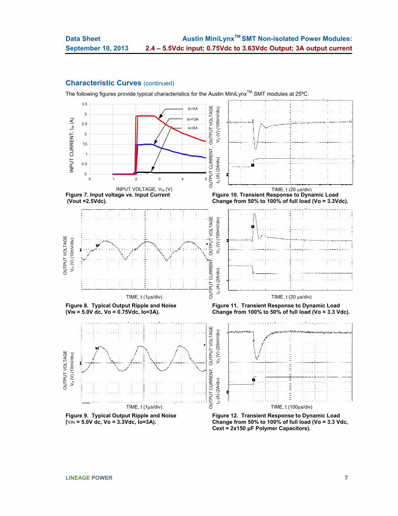
Characteristic Curves
The following figures provide typical characteristics for the Austin MiniLynxTM SMT modules at 25ºC.
EF
FIC
IEN
CY
, η
(%)
70
73
76
79
82
85
88
91
94
0 0.6 1.2 1.8 2.4 3
VIN = 5.0V
VIN = 3.3V
VIN = 2.5V
EF
FIC
IEN
CY
, η
(%)
73
76
79
82
85
88
91
94
97
0 0.6 1.2 1.8 2.4 3
VIN = 5.0V
VIN = 3.3V
VIN = 2.5V
OUTPUT CURRENT, IO (A) OUTPUT CURRENT, IO (A)
Figure 1. Converter Efficiency versus Output Current (Vout = 0.75Vdc).
Figure 4. Converter Efficiency versus Output Current (Vout = 1.8Vdc).
EF
FIC
IEN
CY
, η
(%)
70
73
76
79
82
85
88
91
94
0 0.6 1.2 1.8 2.4 3
VIN = 5.0V
VIN = 3.3V
VIN = 2.5V
EF
FIC
IEN
CY
, η
(%)
OUTPUT CURRENT, IO (A) OUTPUT CURRENT, IO (A)
Figure 2. Converter Efficiency versus Output Current (Vout = 1.2Vdc).
Figure 5. Converter Efficiency versus Output Current (Vout = 2.5Vdc).
EF
FIC
IEN
CY
, η
(%
)
72
75
78
81
84
87
90
93
96
0 0.6 1.2 1.8 2.4 3
VIN = 5.0V
VIN = 3.3V
VIN = 2.5V
EF
FIC
IEN
CY
, η
(%
)
OUTPUT CURRENT, IO (A) OUTPUT CURRENT, IO (A)
Figure 3. Converter Efficiency versus Output Current (Vout = 1.5Vdc).
Figure 6. Converter Efficiency versus Output Current (Vout = 3.3Vdc).
74
77
80
83
86
89
92
95
98
0 0.6 1.2 1.8 2.4 3
VIN = 5.0V
VIN = 4.0V
VIN = 3.3V
75
78
81
84
87
90
93
96
99
0 0.6 1.2 1.8 2.4 3
VIN = 5.5V
VIN = 5.0V
VIN = 4.0V
Data Sheet
September 10, 2013 Austin MiniLynxTM SMT Non-isolated Power Modules:
2.4 – 5.5Vdc input; 0.75Vdc to 3.63Vdc Output; 3A output current
LINEAGE POWER 7
Characteristic Curves (continued)
The following figures provide typical characteristics for the Austin MiniLynxTM SMT modules at 25ºC.
INP
UT
CU
RR
EN
T, I
IN (
A)
0
0.5
1
1.5
2
2.5
3
3.5
0 1 2 3 4 5
Io=1.5A
Io=0A
Io=3A
OU
TP
UT
CU
RR
EN
T,
OU
TP
UT
VO
LTA
GE
I O
(A
) (2
A/d
iv)
VO (
V)
(100
mV
/div
)
INPUT VOLTAGE, VIN (V) TIME, t (20 μs/div)
Figure 7. Input voltage vs. Input Current (Vout =2.5Vdc).
Figure 10. Transient Response to Dynamic Load Change from 50% to 100% of full load (Vo = 3.3Vdc).
OU
TP
UT
VO
LTA
GE
VO (
V)
(10m
V/d
iv)
OU
TP
UT
CU
RR
EN
T,
OU
TP
UT
VO
LTA
GE
I O
(A
) (2
A/d
iv)
VO (
V)
(100
mV
/div
)
TIME, t (1μs/div) TIME, t (20 μs/div)
Figure 8. Typical Output Ripple and Noise (VIN = 5.0V dc, Vo = 0.75Vdc, Io=3A).
Figure 11. Transient Response to Dynamic Load Change from 100% to 50% of full load (Vo = 3.3 Vdc).
O
UT
PU
T V
OLT
AG
E
VO (
V)
(10m
V/d
iv)
OU
TP
UT
CU
RR
EN
T,
OU
TP
UT
VO
LTA
GE
I O
(A
) (2
A/d
iv)
VO (
V)
(20m
V/d
iv)
TIME, t (1μs/div) TIME, t (100μs/div)
Figure 9. Typical Output Ripple and Noise (VIN = 5.0V dc, Vo = 3.3Vdc, Io=3A).
Figure 12. Transient Response to Dynamic Load Change from 50% to 100% of full load (Vo = 3.3 Vdc, Cext = 2x150 μF Polymer Capacitors).

Data Sheet
September 10, 2013 Austin MiniLynxTM SMT Non-isolated Power Modules:
2.4 – 5.5Vdc input; 0.75Vdc to 3.63Vdc Output; 3A output current
LINEAGE POWER 8
Characteristic Curves (continued)
The following figures provide typical characteristics for the Austin MiniLynxTM SMT modules at 25ºC.
OU
TP
UT
CU
RR
EN
T,
OU
TP
UT
VO
LTA
GE
I O (
A)
(2A
/div
)
VO (
V)
(20m
V/d
iv)
INP
UT
VO
LTA
G
O
UT
PU
T V
OLT
AG
E
V
IN (V
) (2
V/d
iv)
V
O (
V)
(1V
/div
)
TIME, t (100μs/div) TIME, t (2ms/div)
Figure 13. Transient Response to Dynamic Load Change from 100% of 50% full load (Vo = 3.3Vdc, Cext = 2x150 μF Polymer Capacitors).
Figure 16. Typical Start-Up with application of Vin (VIN = 5.0Vdc, Vo = 3.3Vdc, Io = 3A).
ON
/OF
F V
OLT
AG
E
O
UT
PU
T V
OLT
AG
E
V
On/
off(V
) (2
V/d
iv)
V
O (
V)
(1V
/div
)
ON
/OF
F V
OLT
AG
E
O
UT
PU
T V
OLT
AG
E
V
On/
off(V
) (2
V/d
iv)
V
O (
V)
(0.5
V/d
iv)
TIME, t (2ms/div) TIME, t (2ms/div)
Figure 14. Typical Start-Up Using Remote On/Off (VIN = 5.0Vdc, Vo = 3.3Vdc, Io = 3A).
Figure 17 Typical Start-Up Using Remote On/Off with Prebias (VIN = 3.3Vdc, Vo = 1.8Vdc, Io = 1.0A, Vbias =1.0Vdc).
ON
/OF
F V
OLT
AG
E
O
UT
PU
T V
OLT
AG
E
V
On/
off(V
) (2
V/d
iv)
V
O (
V)
(1V
/div
)
O
UT
PU
T C
UR
RE
NT
,
IO (
A)
(5A
/div
)
TIME, t (2ms/div) TIME, t (10ms/div)
Figure 15. Typical Start-Up Using Remote On/Off with Low-ESR external capacitors (7x150uF Polymer) (VIN = 5.0Vdc, Vo = 3.3Vdc, Io = 3A, Co = 1050μF).
Figure 18. Output short circuit Current (VIN = 5.0Vdc, Vo = 0.75Vdc).

Data Sheet
September 10, 2013 Austin MiniLynxTM SMT Non-isolated Power Modules:
2.4 – 5.5Vdc input; 0.75Vdc to 3.63Vdc Output; 3A output current
LINEAGE POWER 9
Characteristic Curves (continued)
The following figures provide thermal derating curves for the Austin MiniLynxTM SMT modules.
OU
TP
UT
CU
RR
EN
T, I
o
(A)
0
0.5
1
1.5
2
2.5
3
3.5
20 30 40 50 60 70 80 90
0 LFM
OU
TP
UT
CU
RR
EN
T, I
o
(A)
0
0.5
1
1.5
2
2.5
3
3.5
20 30 40 50 60 70 80 90
0 LFM
AMBIENT TEMPERATURE, TA OC AMBIENT TEMPERATURE, TA OC
Figure 19. Derating Output Current versus Local Ambient Temperature and Airflow (VIN = 5.0, Vo=3.3Vdc).
Figure 22. Derating Output Current versus Local Ambient Temperature and Airflow (VIN = 3.3dc, Vo=2.5 Vdc).
OU
TP
UT
CU
RR
EN
T,
Io
(A)
0
0.5
1
1.5
2
2.5
3
3.5
20 30 40 50 60 70 80 90
0 LFM
0
0.5
1
1.5
2
2.5
3
3.5
20 30 40 50 60 70 80 90
0 LFM
AMBIENT TEMPERATURE, TA OC
Figure 20. Derating Output Current versus Local Ambient Temperature and Airflow (VIN = 5.0Vdc, Vo=1.8 Vdc).
Figure 23. Derating Output Current versus Local Ambient Temperature and Airflow (VIN = 3.3dc, Vo=1.2 Vdc).
OU
TP
UT
CU
RR
EN
T, I
o (
A)
0
0.5
1
1.5
2
2.5
3
3.5
20 30 40 50 60 70 80 90
0 LFM
0
0.5
1
1.5
2
2.5
3
3.5
20 30 40 50 60 70 80 90
0 LFM
AMBIENT TEMPERATURE, TA OC Figure 21. Derating Output Current versus Local Ambient Temperature and Airflow (VIN = 5.0Vdc, Vo=0.75 Vdc).
Figure 24. Derating Output Current versus Local Ambient Temperature and Airflow (VIN = 3.3dc, Vo=0.75 Vdc).

Data Sheet
September 10, 2013 Austin MiniLynxTM SMT Non-isolated Power Modules:
2.4 – 5.5Vdc input; 0.75Vdc to 3.63Vdc Output; 3A output current
LINEAGE POWER 10
Test Configurations
TO OSCILLOSCOPE CURRENT PROBE
LTEST
1μH
BA
TT
ER
Y
CS 1000μF Electrolytic
E.S.R.<0.1Ω
@ 20°C 100kHz
2x100μF Tantalum
VIN(+)
COM
NOTE: Measure input reflected ripple current with a simulated source inductance (LTEST) of 1μH. Capacitor CS offsets possible battery impedance. Measure current as shown above.
CIN
Figure 25. Input Reflected Ripple Current Test Setup.
NOTE: All voltage measurements to be taken at the module terminals, as shown above. If sockets are used then Kelvin connections are required at the module terminals to avoid measurement errors due to socket contact resistance.
V O (+)
COM
1uF .
RESISTIVELOAD
SCOPE
COPPER STRIP
GROUND PLANE
10uF
Figure 26. Output Ripple and Noise Test Setup.
VO
COM
VIN(+)
COM
RLOAD
Rcontact Rdistribution
Rcontact RdistributionRcontact
Rcontact Rdistribution
Rdistribution
VIN VO
NOTE: All voltage measurements to be taken at the module terminals, as shown above. If sockets are used then Kelvin connections are required at the module terminals to avoid measurement errors due to socket contact resistance.
Figure 27. Output Voltage and Efficiency Test Setup.
η =
VO. IO
VIN. IIN x 100 % Efficiency
Design Considerations
Input Filtering
The Austin MiniLynxTM SMT module should be connected to a low-impedance source. A highly inductive source can affect the stability of the module. An input capacitance must be placed directly adjacent to the input pin of the module, to minimize input ripple voltage and ensure module stability.
To minimize input voltage ripple, low-ESR polymer and ceramic capacitors are recommended at the input of the module. Figure 28 shows the input ripple voltage (mVp-p) for various outputs with 1x22µF (TDK: C3225X5R0J226V) ceramic capacitor at the input of the module. Figure 29 shows the input ripple with 1x47µF (TDK: C3225X5R0J476M) ceramic capacitor at full load.
Inp
ut R
ipp
le V
olta
ge
(m
Vp
-p)
0
20
40
60
80
100
120
140
160
0 0.5 1 1.5 2 2.5 3 3.5
3.3Vin
5Vin
Output Voltage (Vdc)
Figure 28. Input ripple voltage for various outputs with 1x22 µF ceramic capacitor at the input (full-load).
Inp
ut R
ipp
le V
olta
ge
(m
Vp
-p)
0
20
40
60
80
100
120
140
160
0 0.5 1 1.5 2 2.5 3 3.5
3.3Vin
5Vin
Output Voltage (Vdc)
Figure 29. Input ripple voltage for various outputs with 1x47 µF ceramic capacitor at the input (full load).

Data Sheet
September 10, 2013 Austin MiniLynxTM SMT Non-isolated Power Modules:
2.4 – 5.5Vdc input; 0.75Vdc to 3.63Vdc Output; 3A output current
LINEAGE POWER 11
Design Considerations (continued)
Output Filtering
The Austin MiniLynxTM SMT module is designed for low output ripple voltage and will meet the maximum output ripple specification with 1 µF ceramic and 10 µF tantalum capacitors at the output of the module. However, additional output filtering may be required by the system designer for a number of reasons. First, there may be a need to further reduce the output ripple and noise of the module. Second, the dynamic response characteristics may need to be customized to a particular load step change.
To reduce the output ripple and improve the dynamic response to a step load change, additional capacitance at the output can be used. Low ESR polymer and ceramic capacitors are recommended to improve the dynamic response of the module. For stable operation of the module, limit the capacitance to less than the maximum output capacitance as specified in the electrical specification table.
Safety Considerations
For safety agency approval the power module must be installed in compliance with the spacing and separation requirements of the end-use safety agency standards, i.e., UL 60950-1, CSA C22.2 No. 60950-1-03, and VDE 0850:2001-12 (EN60950-1) Licensed.
For the converter output to be considered meeting the requirements of safety extra-low voltage (SELV), the input must meet SELV requirements. The power module has extra-low voltage (ELV) outputs when all inputs are ELV.
The input to these units is to be provided with a fast-acting fuse with a maximum rating of 6A in the positive input lead.

Data Sheet
September 10, 2013 Austin MiniLynxTM SMT Non-isolated Power Modules:
2.4 – 5.5Vdc input; 0.75Vdc to 3.63Vdc Output; 3A output current
LINEAGE POWER 12
Feature Description
Remote On/Off
The Austin MiniLynxTM SMT power modules feature an On/Off pin for remote On/Off operation. Two On/Off logic options are available in the Austin MiniLynxTM series modules. Positive Logic On/Off signal, device code suffix “4”, turns the module ON during a logic High on the On/Off pin and turns the module OFF during a logic Low. Negative logic On/Off signal, no device code suffix, turns the module OFF during logic High on the On/Off pin and turns the module ON during logic Low.
For positive logic modules, the circuit configuration for using the On/Off pin is shown in Figure 30. The On/Off pin is an open collector/drain logic input signal (Von/Off) that is referenced to ground. During a logic-high (On/Off pin is pulled high internal to the module) when the transistor Q1 is in the Off state, the power module is ON. Maximum allowable leakage current of the transistor when Von/off = VIN,max is 10µA. Applying a logic-low when the transistor Q1 is turned-On, the power module is OFF. During this state VOn/Off must be less than 0.3V. When not using positive logic On/off pin, leave the pin unconnected or tie to VIN.
Q1
R2
R1Q2
R3
R4
Q3 CSS
GND
VIN+
ON/OFF
PWM Enable
+
_
ON/OFFVI ON/OFF
MODULE
Figure 30. Circuit configuration for using positive logic On/OFF.
For negative logic On/Off devices, the circuit configuration is shown is Figure 31. The On/Off pin is pulled high with an external pull-up resistor (typical Rpull-up = 5k, +/- 5%). When transistor Q1 is in the Off state, logic High is applied to the On/Off pin and the power module is Off. The minimum On/off voltage for logic High on the On/Off pin is 1.5Vdc. To turn the module ON, logic Low is applied to the On/Off pin by turning ON Q1. When not using the negative logic On/Off, leave the pin unconnected or tie to GND.
Q1
R1
R2
Q2 CSS
GND
PWM Enable
ON/OFF
VIN+
ON/OFF
_
+V
I
MODULEpull-upR
ON/OFF
Figure 31. Circuit configuration for using negative logic On/OFF.
Overcurrent Protection To provide protection in a fault (output overload) condition, the unit is equipped with internal current-limiting circuitry and can endure current limiting continuously. At the point of current-limit inception, the unit enters hiccup mode. The unit operates normally once the output current is brought back into its specified range. The typical average output current during hiccup is 2A.
Input Undervoltage Lockout
At input voltages below the input undervoltage lockout limit, module operation is disabled. The module will begin to operate at an input voltage above the undervoltage lockout turn-on threshold.
Overtemperature Protection
To provide over temperature protection in a fault condition, the unit relies upon the thermal protection feature of the controller IC. The unit will shutdown if the thermal reference point Tref, exceeds 140oC (typical), but the thermal shutdown is not intended as a guarantee that the unit will survive temperatures beyond its rating. The module will automatically restart after it cools down.
Output Voltage Programming
The output voltage of the Austin MiniLynxTM SMT can be programmed to any voltage from 0.75 Vdc to 3.63 Vdc by connecting a single resistor (shown as Rtrim in Figure 32) between the TRIM and GND pins of the module. Without an external resistor between TRIM pin and the ground, the output voltage of the module is 0.7525 Vdc. To calculate the value of the resistor Rtrim for a particular output voltage Vo, use the following equation:
Ω
−
−= 5110
7525.021070
VoRtrim

Data Sheet
September 10, 2013 Austin MiniLynxTM SMT Non-isolated Power Modules:
2.4 – 5.5Vdc input; 0.75Vdc to 3.63Vdc Output; 3A output current
LINEAGE POWER 13
Feature Descriptions (continued) Output Voltage Programming (continued)
For example, to program the output voltage of the Austin MiniLynxTM module to 1.8 Vdc, Rtrim is calculated is follows:
−
−= 5110
7525.08.121070
Rtrim
Ω= kRtrim 004.15
V O (+)
TRIM
GND Rtrim
LOAD
V IN (+)
ON/OFF
Figure 32. Circuit configuration to program output voltage using an external resistor.
Table 1 provides Rtrim values required for some common output voltages.
Table 1
VO, set (V) Rtrim (KΩ)
0.7525 Open
1.2 41.973
1.5 23.077
1.8 15.004
2.5 6.947
3.3 3.160
Using 1% tolerance trim resistor, set point tolerance of ±2% is achieved as specified in the electrical specification. The POL Programming Tool, available at www.lineagepower.com under the Design Tools section, helps determine the required external trim resistor needed for a specific output voltage.
Voltage Margining
Output voltage margining can be implemented in the Austin MiniLynxTM modules by connecting a resistor, Rmargin-up, from the Trim pin to the ground pin for
margining-up the output voltage and by connecting a resistor, Rmargin-down, from the Trim pin to the Output pin for margining-down. Figure 33 shows the circuit configuration for output voltage margining. The POL Programming Tool, available at www.lineagepower.com under the Design Tools section, also calculates the values of Rmargin-up and Rmargin-down for a specific output voltage and % margin. Please consult your local Lineage Power technical representative for additional details.
Vo
Austin Lynx or Lynx II Series
GND
Trim
Q1
Rtrim
Rmargin-up
Q2
Rmargin-down
Figure 33. Circuit Configuration for margining Output voltage.

Data Sheet
September 10, 2013 Austin MiniLynxTM SMT Non-isolated Power Modules:
2.4 – 5.5Vdc input; 0.75Vdc to 3.63Vdc Output; 3A output current
LINEAGE POWER 14
Thermal Considerations
Power modules operate in a variety of thermal environments; however, sufficient cooling should always be provided to help ensure reliable operation.
Considerations include ambient temperature, airflow, module power dissipation, and the need for increased reliability. A reduction in the operating temperature of the module will result in an increase in reliability. The thermal data presented here is based on physical measurements taken in a wind tunnel. The test set-up is shown in Figure 35. Note that the airflow is parallel to the long axis of the module as shown in figure 34. The derating data applies to airflow in either direction of the module’s long axis.
Air Flow
Tref
Figure 34. Tref Temperature measurement location.
The thermal reference point, Tref used in the specifications is shown in Figure 34. For reliable operation this temperature should not exceed 115oC.
The output power of the module should not exceed the rated power of the module (Vo,set x Io,max).
Please refer to the Application Note “Thermal Characterization Process For Open-Frame Board-Mounted Power Modules” for a detailed discussion of thermal aspects including maximum device temperatures.
Figure 35. Thermal Test Set-up.
Air flow
x
Power Module
Wind Tunnel
PWBs
5.97_ (0.235)
76.2_ (3.0)
Probe Locationfor measuringairflow andambienttemperature
25.4_ (1.0)

Data Sheet
September 10, 2013 Austin MiniLynxTM SMT Non-isolated Power Modules:
2.4 – 5.5Vdc input; 0.75Vdc to 3.63Vdc Output; 3A output current
LINEAGE POWER 15
Mechanical Outline
Dimensions are in millimeters and (inches).
Tolerances: x.x mm ± 0.5 mm (x.xx in. ± 0.02 in.) [unless otherwise indicated]
x.xx mm ± 0.25 mm (x.xxx in ± 0.010 in.)
Co-planarity (max): 0.102 [0.004]
BOTTOM VIEW SIDE VIEW

Data Sheet
September 10, 2013 Austin MiniLynxTM SMT Non-isolated Power Modules:
2.4 – 5.5Vdc input; 0.75Vdc to 3.63Vdc Output; 3A output current
LINEAGE POWER 16
Recommended Pad Layout
Dimensions are in millimeters and (inches).
Tolerances: x.x mm ± 0.5 mm (x.xx in. ± 0.02 in.) [unless otherwise indicated]
x.xx mm ± 0.25 mm (x.xxx in ± 0.010 in.)
PIN FUNCTION
1 On/Off
2 VIN
3 GND
4 Trim
5 VOUT

Data Sheet
September 10, 2013 Austin MiniLynxTM SMT Non-isolated Power Modules:
2.4 – 5.5Vdc input; 0.75Vdc to 3.63Vdc Output; 3A output current
LINEAGE POWER 17
Packaging Details
The Austin MiniLynxTM SMT version is supplied in tape & reel as standard. Modules are shipped in quantities of 400 modules per reel.
All Dimensions are in millimeters and (in inches).
Reel Dimensions Outside diameter: 330.2 mm (13.00)
Inside diameter: 177.8 mm (7.00”)
Tape Width: 44.0 mm (1.73”)

Data Sheet
September 10, 2013 Austin MiniLynxTM SMT Non-isolated Power Modules:
2.4 – 5.5Vdc input; 0.75Vdc to 3.63Vdc Output; 3A output current
LINEAGE POWER 18
Surface Mount Information
Pick and Place
The Austin MiniLynxTM SMT modules use an open frame construction and are designed for a fully automated assembly process. The modules are fitted with a label designed to provide a large surface area for pick and placing. The label meets all the requirements for surface mount processing, as well as safety standards and is able to withstand maximum reflow temperature. The label also carries product information such as product code, serial number and location of manufacture.
Figure 36. Pick and Place Location.
Nozzle Recommendations
The module weight has been kept to a minimum by using open frame construction. Even so, these modules have a relatively large mass when compared to conventional SMT components. Variables such as nozzle size, tip style, vacuum pressure and pick & placement speed should be considered to optimize this process. The minimum recommended nozzle diameter for reliable operation is 3mm. The maximum nozzle outer diameter, which will safely fit within the allowable component spacing, is 8 mm max.
Tin Lead Soldering
The Austin MiniLynxTM SMT power modules are lead free modules and can be soldered either in a lead-free solder process or a conventional Tin/Lead (Sn/Pb) process. It is recommended that the customer review data sheets in order to customize the solder reflow profile for each application board assembly. The following instructions must be observed when soldering these units. Failure to observe these instructions may result in the failure of or cause damage to the modules, and can adversely affect long-term reliability.
The Austin MiniLynxTM SMT power modules are lead free modules and can be soldered either in a lead-free solder process or a conventional Tin/Lead (Sn/Pb) process. It is recommended that the customer review
data sheets in order to customize the solder reflow profile for each application board assembly. The following instructions must be observed when soldering these units. Failure to observe these instructions may result in the failure of or cause damage to the modules, and can adversely affect long-term reliability.
RE
FL
OW
TE
MP
(°C
) 0
50
100
150
200
250
300
Preheat zonemax 4oCs-1
Soak zone30-240s
Heat zonemax 4oCs-1
Peak Temp 235oC
Coolingzone1-4oCs-1
Tlim above 205oC
REFLOW TIME (S)
Figure 37. Reflow Profile for Tin/Lead (Sn/Pb) process.
MA
X T
EM
P S
OLD
ER
(°C
)
200
205
210
215
220
225
230
235
240
0 10 20 30 40 50 60
Figure 38. Time Limit Curve Above 205oC Reflow for Tin Lead (Sn/Pb) process.

Data Sheet
September 10, 2013 Austin MiniLynxTM SMT Non-isolated Power Modules:
2.4 – 5.5Vdc input; 0.75Vdc to 3.63Vdc Output; 3A output current
LINEAGE POWER 19
Surface Mount Information (continued)
Lead Free Soldering
The –Z version Austin MiniLynx SMT modules are lead-free (Pb-free) and RoHS compliant and are both forward and backward compatible in a Pb-free and a SnPb soldering process. Failure to observe the instructions below may result in the failure of or cause damage to the modules and can adversely affect long-term reliability.
Pb-free Reflow Profile
Power Systems will comply with J-STD-020 Rev. C (Moisture/Reflow Sensitivity Classification for Nonhermetic Solid State Surface Mount Devices) for both Pb-free solder profiles and MSL classification procedures. This standard provides a recommended forced-air-convection reflow profile based on the volume and thickness of the package (table 4-2). The suggested Pb-free solder paste is Sn/Ag/Cu (SAC). The recommended linear reflow profile using Sn/Ag/Cu solder is shown in Figure. 39.
MSL Rating
The Austin MiniLynxTM SMT modules have a MSL rating of 2a.
Storage and Handling The Austin MiniLynxTM modules have a MSL rating of 1. The recommended storage environment and handling procedures for moisture-sensitive surface mount packages is detailed in J-STD-033 Rev. A (Handling, Packing, Shipping and Use of Moisture/Reflow Sensitive Surface Mount Devices). Moisture barrier bags (MBB) with desiccant are
required for MSL ratings of 2 or greater. These sealed packages should not be broken until time of use. Once the original package is broken, the floor life of the product at conditions of ≤ 30°C and 60% relative humidity varies according to the MSL rating (see J-STD-033A). The shelf life for dry packed SMT packages will be a minimum of 12 months from the bag seal date, when stored at the following conditions: < 40° C, < 90% relative humidity.
Post Solder Cleaning and Drying Considerations
Post solder cleaning is usually the final circuit-board assembly process prior to electrical board testing. The result of inadequate cleaning and drying can affect both the reliability of a power module and the testability of the finished circuit-board assembly. For guidance on appropriate soldering, cleaning and drying procedures, refer to Board Mounted Power Modules: Soldering and Cleaning Application Note (AN04-001).
Per J-STD-020 Rev. C
0
50
100
150
200
250
300
Reflow Time (Seconds)
Ref
low
Tem
p (
°C)
Heating Zone 1°C/Second
Peak Temp 260°C
* Min. Time Above 235°C 15 Seconds
*Time Above 217°C 60 Seconds
Cooling Zone
Figure 39. Recommended linear reflow profile using Sn/Ag/Cu solder.
Data Sheet
September 10, 2013 Austin MiniLynxTM SMT Non-isolated Power Modules:
2.4 – 5.5Vdc input; 0.75Vdc to 3.63Vdc Output; 3A output current
LINEAGE POWER 20 Document No: DS04-026 ver. 1.14
PDF name: minilynx_smt_ds.pdf
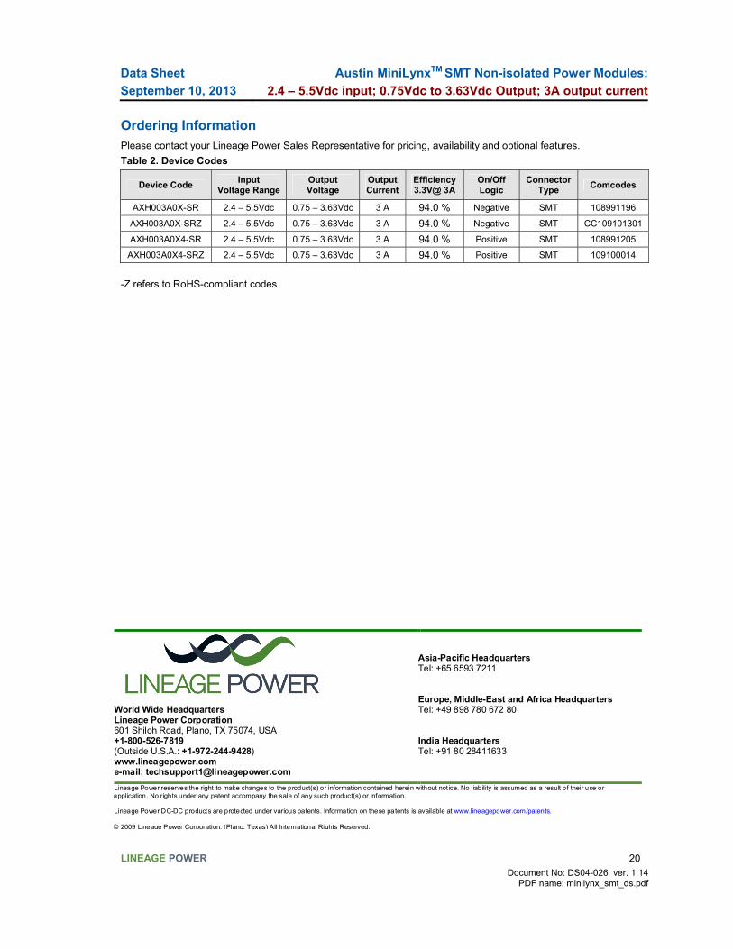
Ordering Information
Please contact your Lineage Power Sales Representative for pricing, availability and optional features.
Table 2. Device Codes
Device Code Input
Voltage Range Output Voltage
Output Current
Efficiency 3.3V@ 3A
On/Off Logic
Connector Type
Comcodes
AXH003A0X-SR 2.4 – 5.5Vdc 0.75 – 3.63Vdc 3 A 94.0 % Negative SMT 108991196
AXH003A0X-SRZ 2.4 – 5.5Vdc 0.75 – 3.63Vdc 3 A 94.0 % Negative SMT CC109101301
AXH003A0X4-SR 2.4 – 5.5Vdc 0.75 – 3.63Vdc 3 A 94.0 % Positive SMT 108991205
AXH003A0X4-SRZ 2.4 – 5.5Vdc 0.75 – 3.63Vdc 3 A 94.0 % Positive SMT 109100014
-Z refers to RoHS-compliant codes
World Wide Headquarters Lineage Power Corporation 601 Shiloh Road, Plano, TX 75074, USA +1-800-526-7819 (Outside U.S.A.: +1-972-244-9428) www.lineagepower.com e-mail: [email protected]
Asia-Pacific Headquarters Tel: +65 6593 7211 Europe, Middle-East and Africa Headquarters Tel: +49 898 780 672 80 India Headquarters Tel: +91 80 28411633
Lineage Power reserves the right to make changes to the product(s) or information contained herein without notice. No liability is assumed as a result of their use or application. No rights under any patent accompany the sale of any such product(s) or information. Lineage Power DC-DC products are protected under various patents. Information on these patents is available at www.lineagepower.com/patents.
© 2009 Lineage Power Corporation, (Plano, Texas) All International Rights Reserved.