Embed Size (px)
Citation preview

IC Manufacturing and Environment: Reducing the
environmental impact
Aun Ahsan
School of Electronic Engineering, Dublin City University, Glasnevin, Dublin 9, Ireland.
Abstract— This paper reviews the semiconductor
manufacturing process of a typical fab, discussing
key steps in the process briefly, front-end-of-line and
back-end-of-line process have been shown. The
environmental impacts of the semiconductor industry
are realized, consumption water, electricity usage
and chemical usage in terms of impact to the
environment, health and safety. Steps to reduce
energy consumption and solutions to reduce and
conserve the amount of water being used have been
discussed, a comparison of savings done before and
after using conservative methods and the reduction
in carbon footprint and the water footprint has been
approximated. Finally conservation and alternative
sustainable energy solutions have been shown.
Keywords—component; Semiconductor
manufacturing process, Fabs, Cz, Fz, Etch, Doping,
Lithography,Epitaxy, Environmental impacts,
Reduction, Re-use, Recycle, RO, RRO, cleanroon.
Water footprint, Carbon Footprint.
I. INTRODUCTION
Since the invention of the transistor by William
Shockley and his colleagues in 1947, the transistor
has been the fundamental building block of modern
electronic devices, modern ICs have several billion
transistor.
The current manufacturing process of
semiconductors takes place in a highly pure
environment, all efforts are done to make sure no
contamination is exposed to the wafers, using water
that is ultra-pure and controlling the environment in
which it is produced to avoid the risk of
contaminants. This is possible by expending mass
amounts of energy, energy for heating, cooling,
operating equipment and the equipment itself takes
significant amount of energy. Water in the form of
De-ionised water and Ultra-pure water (UPW) is
used in every step of the manufacturing process,
UPW can also be used as a humidifier in HVAC
systems for the cleanrooms. Regular water from the
city supply is used for heating, cooling and
cleaning.
The modern manufacturing process of integrated
chips is very extensive and precise, Environmental
impacts of the semiconductor industry is equally
extensive, manufacturing plants can consume
upwards of millions of gallons. Electricity
requirements can cause approx. 53 million kg’s of
CO2 emissions. The emphasis on reducing the
carbon footprint of semiconductor is very
important, using environmentally friendly
manufacturing methods is key in having a
sustainable future.
Using chemicals that are hazardous are also a
problem to health and safety of the locals, fab exhausts and waste water could contain hazardous elements like arsenic. Proper reclamation methods and methods to reduce the use of chemicals could greatly reduce health risks for the workers and among the general public.
II. SEMICONDUCTOR DEVICE MANUFACTURING
Manufacturing of semiconductor devices such as
integrated circuits (ICs) takes place in
Semiconductor fabrication plants, commonly called
a fab, for example Intel fab in leixlip founded in
1989 employs 4500 people. Intel has recently
invested $5 Billion on campus upgrades
technological upgrades to prepare for the latest
generation 300mm wafers [1], the manufacturing
process usually involves front-end-of-line (FEOL)
which refers to formation of transistors, capacitors
and resistors . The processes and manufacturing
methods that take place for the production of ICs
are as follows.
- Silicon wafer fabrication
- Lithography
- Etch
- Doping
- Epitaxy (deposition)
- Packaging
Silicon wafer fabrication widely begins with
the Czochralski silicon growth method (CZ), the CZ
method begins with the melting of high purity
polysilicon nuggets and doping element or alloy
contained in a silica crucible. A crystal seed of ~
12mm in diameter attached to a steel cable is dipped
in silica crucible and gradually drawn upwards
while being rotated simultaneously, this rotating
mechanic draws the molten silicon which solidifies
into a continuous crystal [2]. Necking is a process
used to outgrow dislocations, these dislocation
caused by thermal shock upon contact with the melt
must be eliminated before the full diameter crystal
growth can begin, temperature and pulling speed are
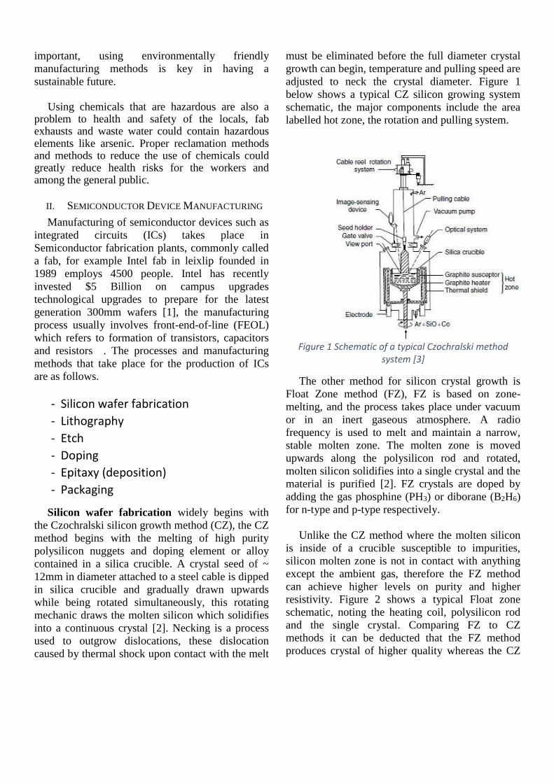
adjusted to neck the crystal diameter. Figure 1
below shows a typical CZ silicon growing system
schematic, the major components include the area
labelled hot zone, the rotation and pulling system.
Figure 1 Schematic of a typical Czochralski method
system [3]
The other method for silicon crystal growth is
Float Zone method (FZ), FZ is based on zone-
melting, and the process takes place under vacuum
or in an inert gaseous atmosphere. A radio
frequency is used to melt and maintain a narrow,
stable molten zone. The molten zone is moved
upwards along the polysilicon rod and rotated,
molten silicon solidifies into a single crystal and the
material is purified [2]. FZ crystals are doped by
adding the gas phosphine (PH3) or diborane (B2H6)
for n-type and p-type respectively.
Unlike the CZ method where the molten silicon
is inside of a crucible susceptible to impurities,
silicon molten zone is not in contact with anything
except the ambient gas, therefore the FZ method
can achieve higher levels on purity and higher
resistivity. Figure 2 shows a typical Float zone
schematic, noting the heating coil, polysilicon rod
and the single crystal. Comparing FZ to CZ
methods it can be deducted that the FZ method
produces crystal of higher quality whereas the CZ

produces wafers that are more cost-efficient. More
importantly the CZ method is easily doped and is
the key advantage it holds over the FZ method and
secures its market share.
Figure 2 Float zone Crystal growth system schematic [3]
Following the growth of the crystal the shaping
process is used to turn the roughed ingot into a
uniform diameter using an industrial-grade diamond
grind. The ingot is grown slightly large to account
for the grinding, the seed and the opposite tang end
are removed and recycled. The wafer slicing takes
place after shaping, x-ray diffraction is used to
determine the orientation of the ingot and inner
diameter circular saw is used to cut while rigidly
mounted in the accurate position. Newer techniques
like wire saw greatly reduce mechanical damage
caused by conventional cutting methods, wire saw
employs diamond coated wires to cut the crystal
into wafers. Figure 3 shows a typical basic wire saw
schematic. Innovation in wires saw technology
improves the quality of the wafer even more by
using a rocking movement of the rotating rollers
and a multi wire set-up [4].
Figure 3 Wire saw
Chemical etching is done to remove mechanical
damage caused by shaping. Mixtures of
hydrofluoric, nitric and acetic acids are used for
acidic solution and caustic etchants like KOH are
used for alkaline etching. Wafer is rinsed post etch
in water. Edge rounding can be used to greatly
reduce mechanical damage.
Wafer polishing is the final step in wafer
production which provides a smooth surface for
further processes. Wafers are mounted under
pressure, pressed against pads and rotated, the two
pads are used for double sided polishing on opposite
spin with a polishing slurry and water mixture
added to the pad. Wafer is then cleaned to remove
the slurry contaminants and organic and metal
impurities are removed. The wafer is inspected to
meet the required specification using Optical
microscopy and Fourier transform infra-red
spectroscopy among other techniques .
Front-end-of-line (FOEL) processing occurs
after the crystal is grown, sliced and polished.
Figure 4 shows FOEL process which includes,
thermal oxidation to produce a thin layer of oxide
on the wafer, photolithography to define useful
shapes on the surface, etching of the unwanted
material and then finally doping the wafer with
impurities to modulate the electrical properties of
the semiconductor.
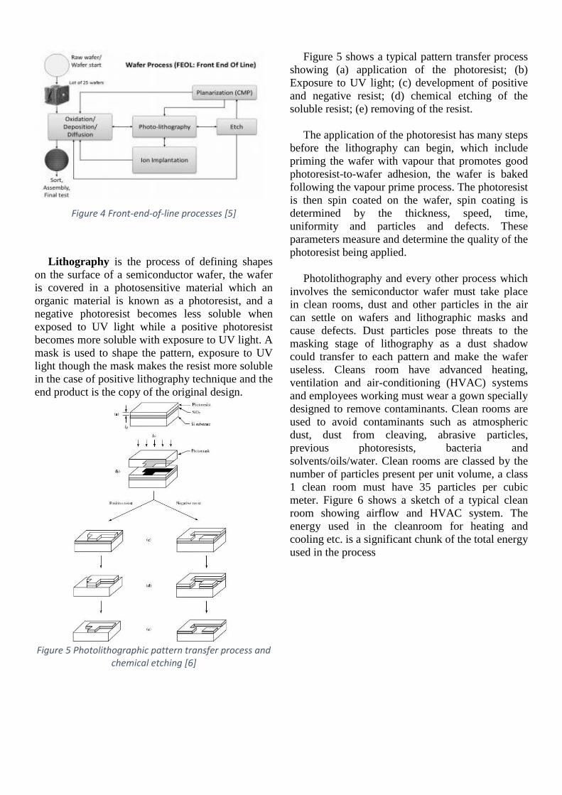
Figure 4 Front-end-of-line processes [5]
Lithography is the process of defining shapes
on the surface of a semiconductor wafer, the wafer
is covered in a photosensitive material which an
organic material is known as a photoresist, and a
negative photoresist becomes less soluble when
exposed to UV light while a positive photoresist
becomes more soluble with exposure to UV light. A
mask is used to shape the pattern, exposure to UV
light though the mask makes the resist more soluble
in the case of positive lithography technique and the
end product is the copy of the original design.
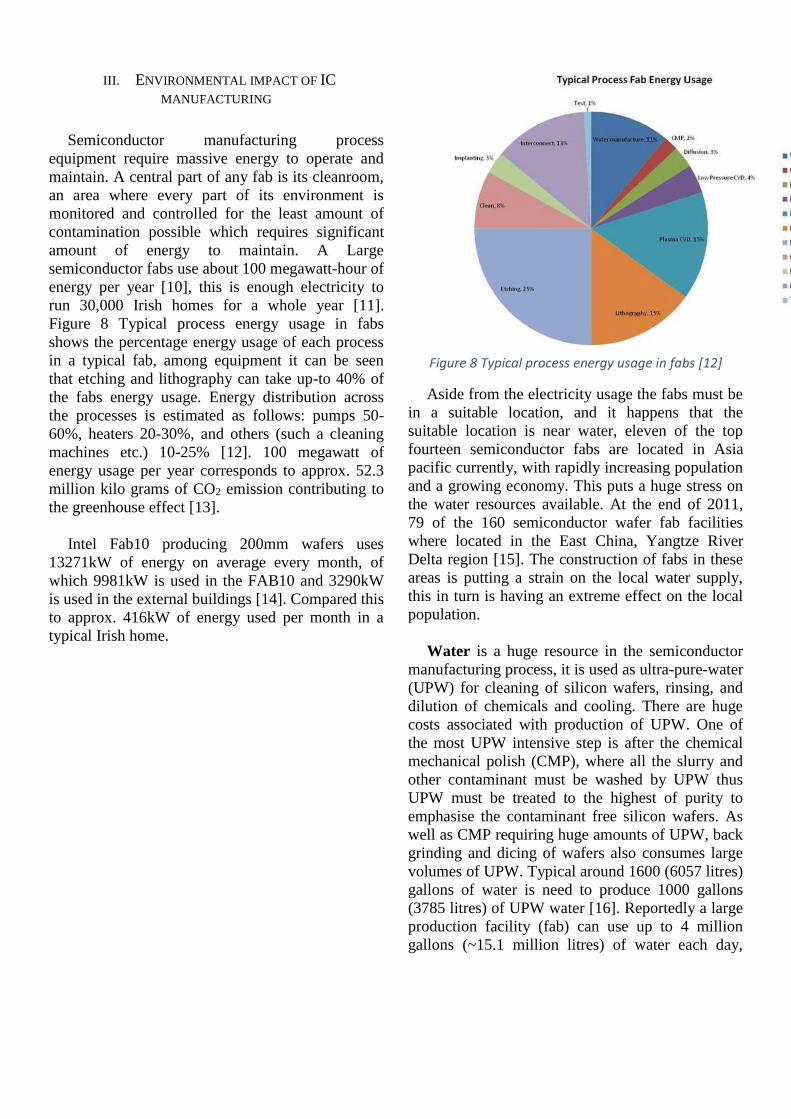
Figure 5 Photolithographic pattern transfer process and
chemical etching [6]
Figure 5 shows a typical pattern transfer process
showing (a) application of the photoresist; (b)
Exposure to UV light; (c) development of positive
and negative resist; (d) chemical etching of the
soluble resist; (e) removing of the resist.
The application of the photoresist has many steps
before the lithography can begin, which include
priming the wafer with vapour that promotes good
photoresist-to-wafer adhesion, the wafer is baked
following the vapour prime process. The photoresist
is then spin coated on the wafer, spin coating is
determined by the thickness, speed, time,
uniformity and particles and defects. These
parameters measure and determine the quality of the
photoresist being applied.
Photolithography and every other process which
involves the semiconductor wafer must take place
in clean rooms, dust and other particles in the air
can settle on wafers and lithographic masks and
cause defects. Dust particles pose threats to the
masking stage of lithography as a dust shadow
could transfer to each pattern and make the wafer
useless. Cleans room have advanced heating,
ventilation and air-conditioning (HVAC) systems
and employees working must wear a gown specially
designed to remove contaminants. Clean rooms are
used to avoid contaminants such as atmospheric
dust, dust from cleaving, abrasive particles,
previous photoresists, bacteria and
solvents/oils/water. Clean rooms are classed by the
number of particles present per unit volume, a class
1 clean room must have 35 particles per cubic
meter. Figure 6 shows a sketch of a typical clean
room showing airflow and HVAC system. The
energy used in the cleanroom for heating and
cooling etc. is a significant chunk of the total energy
used in the process

Figure 6 a typical cleanroom set-up [7]
Doping is a process used to introduce impurities
to a highly pure semiconductor to modulate its
electrical properties. Extrinsic semiconductor is the
name given to the semiconductors that was lightly
doped and semiconductor that are highly doped are
called degenerates.
Some dopants are added to the silicon as it is
grown (in the CZ method for example), selected
areas of the semiconductor are doped following the
photolithography stage with processes like diffusion
and implantation. The basic diffusion process is
typically done by placing the semiconductor in a
controlled, high temperature quartz-tube furnace
and passing a gas mixture through it. Boron is a
commonly used dopant for p-type impurity whereas
arsenic and phosphorus are used for n-type [8].
Dopants can be used in various forms, gases, liquids
and solids, although liquids is the most commonly
used form (BBr3, AsCl3). For ion implantation,
energetic charged particles are introduced into the
silicon. The implantation energies can vary the
depth of the implantation. Ion implantation gives
more control and reproducibility of impurity
doping, ion implantation has a lower processing
temperature as compared with diffusion process.
Epitaxy (Deposition), in epitaxial growth
techniques two major steps are found, Chemical
vapour deposition (CVD) also called vapour-phase
Epitaxy and Molecular beam Epitaxy. CVD can be
at atmospheric pressure (APCVD) or low pressure
(LPCVD), the steps involved in CVD are (i) gases
and dopants are transported into the substrate (Si)
region; (ii) they are absorbed onto the substrate
region; (iii) chemical reaction takes place, catalysed
at the surface and growth of epitaxial layer; (iv) the
gaseous products are desorbed into the main gas
stream and transported out of the reaction chamber.
In VPE Silicon is most commonly deposited from
silicon tetrachloride (SiCl4) in hydrogen although
silane (SiH4), dichlorosilane (SiH2Cl2) and
trichlorosilane (SiHCL3), the typical reaction
temperature for silicon tetrachloride is 1200o C.
Equation below shows the reaction.
SiCL4 (gas) + 2H2 (gas) ↔ Si (solid) + 4HCL (gas)
Molecular beam Epitaxy (MBE) process involves
the reaction of one or more thermal beams of atoms
with a crystalline surface under ultrahigh-vacuum
condition [9]. MBE can achieve a precision control
over chemical composition and doping profiles.
Consequently MBE growth rates are very low.
Following the deposition steps, other key
processes must take place to main a high-quality
products, these include electrical testing and
packaging. Automated test equipment (ATE) is
used to apply measurement stimulus to the chip and
record results. Die separation is done with diamond
saws to scribe or completely separate the dies.
Packaging is responsible for interconnecting,
powering, cooling and protecting the IC. Packaging
acts like the IC’s body and IC itself is the body.
Dual in-line package (DIP) were used as primary
packaging of ICs , with increasing need for more
interconnects and I/O connections pin grid array
(PGA) are being used. Figure 7 shows the DIP and
PGA package types.
Figure 7(left) Dual in-line package (right) Pin
grid array
III. ENVIRONMENTAL IMPACT OF IC
MANUFACTURING
Semiconductor manufacturing process
equipment require massive energy to operate and
maintain. A central part of any fab is its cleanroom,
an area where every part of its environment is
monitored and controlled for the least amount of
contamination possible which requires significant
amount of energy to maintain. A Large
semiconductor fabs use about 100 megawatt-hour of
energy per year [10], this is enough electricity to
run 30,000 Irish homes for a whole year [11].
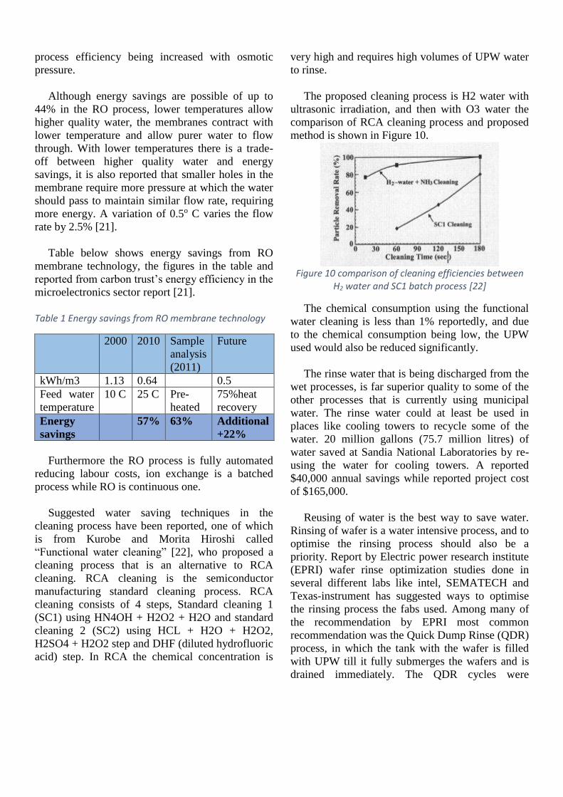
Figure 8 Typical process energy usage in fabs
shows the percentage energy usage of each process
in a typical fab, among equipment it can be seen
that etching and lithography can take up-to 40% of
the fabs energy usage. Energy distribution across
the processes is estimated as follows: pumps 50-
60%, heaters 20-30%, and others (such a cleaning
machines etc.) 10-25% [12]. 100 megawatt of
energy usage per year corresponds to approx. 52.3
million kilo grams of CO2 emission contributing to
the greenhouse effect [13].
Intel Fab10 producing 200mm wafers uses
13271kW of energy on average every month, of
which 9981kW is used in the FAB10 and 3290kW
is used in the external buildings [14]. Compared this
to approx. 416kW of energy used per month in a
typical Irish home.
Figure 8 Typical process energy usage in fabs [12]
Aside from the electricity usage the fabs must be
in a suitable location, and it happens that the
suitable location is near water, eleven of the top
fourteen semiconductor fabs are located in Asia
pacific currently, with rapidly increasing population
and a growing economy. This puts a huge stress on
the water resources available. At the end of 2011,
79 of the 160 semiconductor wafer fab facilities
where located in the East China, Yangtze River
Delta region [15]. The construction of fabs in these
areas is putting a strain on the local water supply,
this in turn is having an extreme effect on the local
population.
Water is a huge resource in the semiconductor
manufacturing process, it is used as ultra-pure-water
(UPW) for cleaning of silicon wafers, rinsing, and
dilution of chemicals and cooling. There are huge
costs associated with production of UPW. One of
the most UPW intensive step is after the chemical
mechanical polish (CMP), where all the slurry and
other contaminant must be washed by UPW thus
UPW must be treated to the highest of purity to
emphasise the contaminant free silicon wafers. As
well as CMP requiring huge amounts of UPW, back
grinding and dicing of wafers also consumes large
volumes of UPW. Typical around 1600 (6057 litres)
gallons of water is need to produce 1000 gallons
(3785 litres) of UPW water [16]. Reportedly a large
production facility (fab) can use up to 4 million
gallons (~15.1 million litres) of water each day,

where 2200 gallons (8328 litres) of can be used to
create and integrated chip on a 30cm wafer approx.
1500 gallons of UPW . Many fabs have their own
treatment to produce UPW and must go through
many chemical engineering unit operations
designed to remove contaminants to reach ultrapure
level. Lithography rinsing of the wafers is the most
water intensive process which requires the use
UPW, Local city water is used in most cases to
produce UPW in fabs. Figure 9 shows the extensive
process of filtering water to produce UPW by using
city water as source.
Figure 9 UPW filtration process [17]
Chemicals, Solvents and gases used from the
semiconductor manufacturing process can be
hazardous. Arsenic, a toxic element is widely used
as a principle component in semiconductor substrate
such as gallium arsenide. Poisonous dopants such as
antimony and phosphorus, poisonous compounds
such as hydrogen peroxide, hydrofluoric acid are
some of the dangerous chemicals being used in the
manufacturing process, it is vital for workers to not
be directly exposed to these chemicals.
Perflourocompound (PFC) gases such as CF4, C2F6,
C3F8, C4F8, CHF3, NF3 and SF6 are used as
chemical precursors in the semiconductor
manufacturing, during the Chemical Vapour
Deposition (CVD) chambers cleaning process , and
is also being used for plasma etching in interconnect
materials. PFCs are greenhouse gases, and
contribute to the greenhouse effect once in the
atmosphere. PFCs are problematic to destroy as
they have strong chemical bonds, for example SF6
has an estimated lifetime of 3,500 years [18].
In an ISMI technology report [19] there is
speculation that future technologies that may bring
more PFC usage include atmospheric downstream
plasma etching (ADP), the shrinking size of
electronic products requires packaging of integrated
circuits to be very small, ADP is used to reduce die
thickness, it is however not clear that ADP will be
the technology of choice for reducing die thickness.
IV. REDUCING ENVIRONMENTAL IMPACT OF THE
SEMICONDUCTOR INDUSTRY
A. Reducing the water footprint
There is constant emphasis that a semiconductor
manufacturing plant can use as much water as a
small city [20], this statement is not further from the
truth. Noted before in this paper that manufacturing
of an integrated chip uses 1500 gallons of UPW
water and a fab can use millions of gallons of water
a day. Clearly conserving water resources should be
top priority among manufacturers, there are number
of ways to conserve and reduce the amount of water
being used in fabs through using better upgraded
equipment and better management.
In Figure 9 one of the steps on the way to UPW
is RO (reverse osmosis) although the figure shows
ion exchange, in modern filtration to UPW, RO and
RRO (recovery reverse osmosis) have taken over
the ion exchange step. It involves removing of
dissolved solids from the water by forcing water
through a semi-permeable membrane. This process
depending on the waters ion content, rejects 25% of
the feed water and achieves a 99.99% purity [21].
The modern thin-film membranes for RO are 15%
more efficient than the old membranes. Heated
water is required in for some parts of the
manufacturing process for example controlling of
the etchant rates, if water was to be preheated
before RO process specific power would be reduced
from 0.78kWh/m3 to 0.43kWh/m3 as reported by
carbon trust in their Industrial Energy Efficiency
accelerator – guide to the microelectronics sector
report of 2013 [12]. This is due to the osmotic
pressure increasing whilst heated and deionisation
process efficiency being increased with osmotic
pressure.
Although energy savings are possible of up to
44% in the RO process, lower temperatures allow
higher quality water, the membranes contract with
lower temperature and allow purer water to flow
through. With lower temperatures there is a trade-
off between higher quality water and energy
savings, it is also reported that smaller holes in the
membrane require more pressure at which the water
should pass to maintain similar flow rate, requiring
more energy. A variation of 0.5o C varies the flow
rate by 2.5% [21].
Table below shows energy savings from RO
membrane technology, the figures in the table and
reported from carbon trust’s energy efficiency in the
microelectronics sector report [21].
Table 1 Energy savings from RO membrane technology
2000 2010 Sample
analysis
(2011)
Future
kWh/m3 1.13 0.64 0.5
Feed water
temperature
10 C 25 C Pre-
heated
75%heat
recovery
Energy
savings
57% 63% Additional
+22%
Furthermore the RO process is fully automated
reducing labour costs, ion exchange is a batched
process while RO is continuous one.
Suggested water saving techniques in the
cleaning process have been reported, one of which
is from Kurobe and Morita Hiroshi called
“Functional water cleaning” [22], who proposed a
cleaning process that is an alternative to RCA
cleaning. RCA cleaning is the semiconductor
manufacturing standard cleaning process. RCA
cleaning consists of 4 steps, Standard cleaning 1
(SC1) using HN4OH + H2O2 + H2O and standard
cleaning 2 (SC2) using HCL + H2O + H2O2,
H2SO4 + H2O2 step and DHF (diluted hydrofluoric
acid) step. In RCA the chemical concentration is
very high and requires high volumes of UPW water
to rinse.
The proposed cleaning process is H2 water with
ultrasonic irradiation, and then with O3 water the
comparison of RCA cleaning process and proposed
method is shown in Figure 10.
Figure 10 comparison of cleaning efficiencies between
H2 water and SC1 batch process [22]
The chemical consumption using the functional
water cleaning is less than 1% reportedly, and due
to the chemical consumption being low, the UPW
used would also be reduced significantly.
The rinse water that is being discharged from the
wet processes, is far superior quality to some of the
other processes that is currently using municipal
water. The rinse water could at least be used in
places like cooling towers to recycle some of the
water. 20 million gallons (75.7 million litres) of
water saved at Sandia National Laboratories by re-
using the water for cooling towers. A reported
$40,000 annual savings while reported project cost
of $165,000.
Reusing of water is the best way to save water.
Rinsing of wafer is a water intensive process, and to
optimise the rinsing process should also be a
priority. Report by Electric power research institute
(EPRI) wafer rinse optimization studies done in
several different labs like intel, SEMATECH and
Texas-instrument has suggested ways to optimise
the rinsing process the fabs used. Among many of
the recommendation by EPRI most common
recommendation was the Quick Dump Rinse (QDR)
process, in which the tank with the wafer is filled
with UPW till it fully submerges the wafers and is
drained immediately. The QDR cycles were
recommended to be reduced to 4 cycles to optimise
the rinsing process. The standard rinsing process
was 10minutes long and required 450 litres of
UPW, this process was suggested to be reduced by
2 minutes saving 100 litres approximately. Nearly
all rinsing processes like post-SPM rinse (sulphur
acid peroxide mixture), post SC1 (standard clean)
and SC2 rinsing were using too much time to rinse
resulting in higher amount of UPW being used, and
each process was reported to save 2-3million litres
of UPW.
B. Reducing Electricity usage
Electricity usage is another huge area of
consumption in the Semiconductor industry, with
equipment costing in millions and requiring massive
amount of electricity to power, as well as cleanroom
having to constantly be expending electricity to be
able to control the environment to have less than 36
particles/m3. Energy consumption in terms of
electricity is a huge window of opportunity to
reduce cost and reduce the carbon emissions of the
fab.
Cleanrooms energy savings could be done by
following the guidelines ISO 14644 for air
exchange rates to keep the required cleanliness, ISO
14644 suggest an air change rate of 240-600 times,
for class 2-class 5 clean rooms. Class 5 clean rooms
are used as work zones, masks, semiconductor
service zones etc., while class 2 can clean enough to
be used for lithography. There are other
requirements that must be completed before a room
can be classified in a class 1 – 8, but air change
rates have high electricity consumption rate and
using the ISO recommended could save allot of
electricity.
Clean room shape and size is directly related to
how much energy is used in it. A bigger clean room
requires more energy to maintain than a smaller
one, due to higher volumes of air that needs to be
changed and maintained. To optimise the cleanroom
and reduce energy consumption, cleanroom should
be exact measurement of the area that is needed.
ISO 5 cleanrooms could be employed using
modular cleanroom technology, a relatively low-
cost solution to cleanrooms that have expandable
capabilities [23].
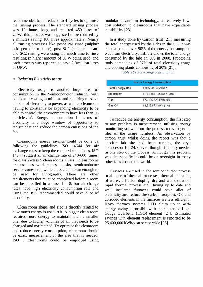
In a study done by Carbon trust [21], measuring
the total energy used by the Fabs in the UK it was
calculated that over 90% of the energy consumption
was from electricity, Table 2 shows the total energy
consumed by the fabs in UK in 2008. Processing
tools composing of 37% of total electricity usage
and cooling plants composing of 20% [21]. Table 2 Sector energy consumption
To reduce the energy consumption, the first step
to any problem is measurement, utilising energy
monitoring software on the process tools to get an
idea of the usage numbers. An observation by
carbon trust whilst doing the report was that a
specific fab site had been running the cryo
compressor for 24/7, even though it is only needed
in one step of the process. Although this problem
was site specific it could be an oversight in many
other fabs around the world.
Furnaces are used in the semiconductor process
in all sorts of thermal processes, thermal annealing
of wafer, diffusion doping, dry and wet oxidation,
rapid thermal process etc. Having up to date and
well insulated furnaces could save allot of
electricity and reduce the carbon footprint. Old and
corroded elements in the furnaces are less efficient ,
Koyo thermos systems LTD claim up to 40%
energy saving is possible with their patented Light
Gauge Overbend (LGO) element [24]. Estimated
savings with element replacement is reported to be
25,400,000 kWh/year sector wide [25].

C. Reducing Perflourocompound emissions
PFCs gases are used as chemical precursors in
semiconductor manufacturing. Compounds like
C2F6 and NF3 used in CVD chambers that have a
10,000 and 740 year atmospheric lifetime
respectively and compounds like CF4 (50,000 year
atmospheric lifetime) and SF6(3,200 year
atmospheric lifetime) being used plasma etching of
interconnect materials. Manufacturing process uses
high global warming potential fluorinated
compounds, it is important for the industry to
reduce PFCs as the semiconductor industry has
been the fastest growing industry.
The European semiconductor industry
association’s (ESIA) voluntary agreement to reduce
PFC emissions have reported a 44% reduction
below the 1995 baseline. Table 3 below shows the
PFCs being used and the relative GWPs of the gases
compared to carbon dioxide.
Table 3 GWPs of gases used in the manufacturing processes as compared to carbon dioxide [26].
Compound Chemical
Formula
Global
warming
potential
(100
years)
Tetraflouromethane CF4 7390
Hexaflouroethane C2F6 12200
Octoflouropropane C3F8 8830
Octoflourocyclobutane c-C4F8 10300
Nitrogen Triflouride NF3 22800
Triflouromethane CHF3 14800
ESIA’s emission reduction technology
development involved, process optimisation,
alternative processing chemistries, capture and
recovery and abatement.
Process optimisation focused on CVD chamber
cleaning , where endpoint detection or extractive
metrology are used to monitor emissions and
provide clean end point times are minimised by
adjusting process parameters like chamber pressure,
temperature , plasma power [27]. Process
optimisation has reported emission reduction of up
to 10-56% [28]. Process optimisation reduced PFC
emission in old fabs and ensured that chamber
cleaning processes minimise gas consumption.
Alternative Processing Chemistries NF3
remote plasma clean technologies have replaced
CF4 and C2F6 chamber clean. Although NF3 has a
higher GWP as shown in Table 3, the higher
utilisation efficiency of 95-99% (meaning most gas
is used and not released to the atmosphere), NF3
makes it a better choice and have reduced PFC
emissions by 95%. This is due to the reduction in
clean times, reduce wet cleaning frequency [29].
Capture and recovery method has been pitched
and results have shown not to be cost effective, NF3
has very low volume of PFC being released for
recovery. Other PFC capture and recovery methods
include Air Liquide PFC capture, a compact
membrane capture and recirculation system for SF6.
The Air Liquide unit compresses the exhaust, which
is then fed into the membrane separation units. Air
Liquide report an 89% SF6 recovery at a little over
99% purity [30].
Abatement of PFCs have been undergoing many
new technologies, the industry has favoured point of use (POU) methods over the end of process (EOP) abatement methods for PFCs, most abetment technologies are able to be applied to in both the etch and the CVD processes. Some methods include Burn-Wet Abatement, Catalytic PFC abatement and Plasma Abatement techniques. These three methods are all POU, Burn-Wet method is the primary POU abatement technology. Fuel-Fired combustor followed by a wet scrubber to capture HF, the Burn-Wet method can be configured to abate C2F6, C3F8, NF3, and SF6.
V. SUSTAINABILITY PROPOSAL
Burning of fossil fuels and oil mining to generate
our energy is causing mass disturbances in the
climate, Due to greenhouse gases the drastic change

in the planets climate is becoming more visible day
by day. Global change in temperature is causing
tornadoes, hurricanes and tsunamis more often. It is
imperative that manufacturers use alternate
sustainable energy sources like wind, hydroelectric,
and solar power.
Fabs simply consume allot more power than
solar power could supply, Intel fab10 as explained
in the environmental impact section of the paper,
consumes 13271kW of electric energy per month,
3290kW of which is spent in office buildings. Solar
power solutions like the new product from Tesla the
PowerWall Lithium ion battery could easily manage
the electric energy being used in the offices. Tesla’s
PowerWall [31] battery provides 6kWh power
output and can work in parallel with more
PowerWalls to provide a larger output. Assuming
all energy is supplied by solar power savings of up
to 24% is possible by using solar power for a part of
the total energy usage.
Solar power efficiency is at around 20-30% for
commercial solar PV cells, while newer
technologies like perovskite solar cells have shown
rapid efficiency growth in the past 3 years.
However as it stands, the solar power efficiency is
not high enough at the moment vs its cost to be
applied to large factories. Tesla and ABB factory in
Finland are constructing factories largely operating
on solar power. Tesla is reportedly spending
$5Billion to construct the factory and is expected to
be done by 2016 as reported by Tesla.
VI. CONCLUSION
The demand of Semiconductor IC products is
increasing extremely rapidly, and each time a newer
technology that must be implemented new process
equipment must be used, costing in the billions.
There is room for allot of optimisation within the
industry to save energy wherever possible,
processes like etching and lithography use
incredible amount of water, which must be treated
to ultra-high purity. There is many conservation
techniques and methods that re-use water like
functional water method to replace the Stand
cleaning procedures that RCA cleaning requires,
using optimised rinsing could save millions of
gallons of water.
Electric energy used in the process equipment is
also being abused by some equipment that only are
required for one step and yet they are operating
24/7, smart procedural equipment management
must be utilized in today’s fabs to reduce energy
usage where ever possible. Clean rooms are the
most energy intensive part of any fab, requiring
energy 24/7. Using energy efficient process
equipment and manufacturers of equipment must
take initiative to bring forth efficient equipment.
All is not bad however, fabs around the world are
reporting reduction in energy usage, and water usage. Intel’s plant in Chandler Arizona have reported reduction in water usage from 5 million gallons of water to 1 million gallons by using Reverse osmosis techniques to return water to the municipal supply [32]. Fabs around the world should use similar techniques to return water, especially in locations where water is scarce.
By using all or some of the methods and techniques mentioned in this report, manufacturers can ensure a lower strain on the environment, without an impact on the quality of the semiconductor process.
ACKNOWLEDGMENT
I would like to thank my lecturer Mr. Paul Ahern of School of engineering in Dublin City University for his proposal of the review topic and for explaining many of the processes in the semiconductor manufacturing. I would also like to thank Dr. Stephen Daniels for module support.

REFERENCES
[1] “Intel Leixlip,” Intel, 2014. [Online].
Available: http://www.intel.ie/content/www/ie
/en/company-overview/about-intel-ireland.html.
[2] R. D. Yoshio Nishi, in
Handbook of semiconductor manufacturing
technology, CRC, 2007, p. chptr 3 page 1.
[3] R. D. Yoshio Nishi, in
Handbook of semiconductor manufacturing
technology, CRC press, 2007, p. chptr 3 page 4.
[4] T. M. W. Saws, “diamond wire saw,”
Takatori Multi Wire Saws, [Online].
Available: http://www.gti-usa.com/semi/product-
category/diamond-wire-saws/.
[5] J. b. S. D.-p. P. V. Claude Yugma,
“Integration of Scheduling and Advanced Process
Control in Semiconductor Manufacturing:
Review and Outlook,” IEEE, Taipe, Taiwan, 2014.
[6] Gary S. May, Costas, J. Spanos, “
Fundamentals of Semiconductor manufacturing
and process control,” in Fundamentals of
Semiconductor manufacturing and process control,
Wiley-IEEE press, 2006, p. 42.
[7] M. design. [Online]. Available: http://www.globalspec.com/ImageRepository/
LearnMore/201211/clean12901b753456b48ed89
c507e39d286862.png.
[8] Gary S. May Simon M. Sze , “Basic diffusion process,
” in Fundamentals of Semiconductor Manufacturing,
Wiley and sons, pp. 106-107.
[9] gary s may, simon m Sze, “Molecular beam epitaxy,”
in fundamentals of semiconductor manufacturing,
Wiley and sons, 2006, pp. 148-149.
[10] A. G. F. W. Steve chen, “Bringing energy effiency
to the fab,” McKinsley & company, pp. 52-55, 2013.
[11] “according to SEAI energy consumption in
the residential area report at 416kWh per month on
average”.
[12] c. trust, “Industrial Energy Efficiency accelterator –
guide to the microelectronics sector,” Carbon trust,
london, 2011.
[13] SEAI, “Sustainable energy authority ireland,” SEAI, 2012.
[Online]. Available: http://www.seai.ie/Your_Business/Public_Sector/FAQ/
Energy_Reporting_Overview/What_are_the_carbon_
emission_factors_used.html.
[14] John fingleton, “Intel Ireland Sustainable energy report,
” SEAI, Dublin, 2003.
[15] c. w. risk, “8 thngs you should know about water &
semiconductors,” chinawaterrisk, july 2013. [Online].
Available: http://chinawaterrisk.org/resources/analysis-
reviews/8-things-you-should-know-about-water-and-
semiconductors/. [Accessed 19 11 2015].
[16] M. V. J. Klusewitz Greg, “Water usage reduction in a
semiconductor fabricator,” IEEE, Cote, 2002.
[17] wikart, “UPW schematic used in semiconductor industry,”
wikipedia, [Online]. Available: https://upload.wikimedia.
org/wikipedia/commons/thumb/9/97/UPW_P%26iD.jpg/700px-UPW_P%26iD.jpg.
[18] S. Raoux, “Strategies for Cost Effective Implementatio
n of PFC Emissions Reduction Solutions in the
Semiconductor industry,” IEEE, 2006.
[19] ISMI, “Reduction of Perflourocompount emission,”
SEMATCH, Austin, TX, 2005.
[20] IEEE spectrum, “Semiconductor manufacturing
plants can use as much water a small city,” 31 aug
2009. [Online]. Available: http://spectrum.ieee.org/
podcast/semiconductors/design/semicondutor-manu
facturing-plants-can-use-as-much-water-as-a-small-ci
ty. [Accessed 11 11 2015].
[21] carbon trust, “Industrial Energy Efficiency accelerator
- guide to microelectronics sector,” Carbon trust , pp.
20-30, 2011.
[22] H. M. Hiroshi Kurobe, “Drastic reduction of chemical
consumption in wet cleaning process for
semiconductor manufacturing by using functional
water,” IEEE, Tokyo, Japan, 2005.
[23] cleanwall, “modular cleanrooms,” [Online].
Available: http://www.cleanroom-solutions.com
/softwall-cleanroom/.
[24] Koyo thermo systems, “Koyo Thermo Systems
Products,” Crystec, [Online]. Available:
https://www.crystec.com/kllgoe.htm.
[25] C. trust, “Industrial Energy Efficiency Accelerator –
Guide to the microelectronics sector,” Carbon trust,
vol. 1, no. 1, p. 31, 2013.
[26] I. p. o. c. change, “Fourth assesment report IPCC section
2.10.2,” Cambridge university press, cambridge , UK, 2007.
[27] European Semiconductor Industry Association,
“The European Semiconductor Industry’s voluntary
agreement to reduce ‘Perfluorocompound’ emissions,”
ESIA, 2006.

[28] C. Allgood, S. Hsu, B. Birmingham, and J. Soucy,
“A Partnership for PFC Emissions Reductions,”
SEMICON Southwest, 2000.
[29] L. M. P. T. B. Chris Nauert, “Reduced Clean Time and PFC
Emissions Reduction through Remote Plasma Clean for
Lamp Heated CVD Chambers,” electrochem.org, Austin,
TX, 2002.
[30] ISMI, “Reduction of Perfluorocompound (PFC) Emissions:
2005 State-ofthe-Technology report,” SEMATECH, Austin,
TX, 2005.
[31] PowerWall, “Powerwall,” Tesla, 24 08 2015. [Online].
Available: https://www.teslamotors.com/POWERWALL.
[Accessed 11 11 2015].
[32] Anna M. Sandoval, “An Application for Treating S
emiconductor Manufacturing Industrial Wastewater
to Environmental Protection Agency Drinking Water
Standards,” INTEL CORPORATION, Chandler, AZ.


