Embed Size (px)
Citation preview

Auger Electron Spectroscopy
(AES)
Prof. Paul K. Chu
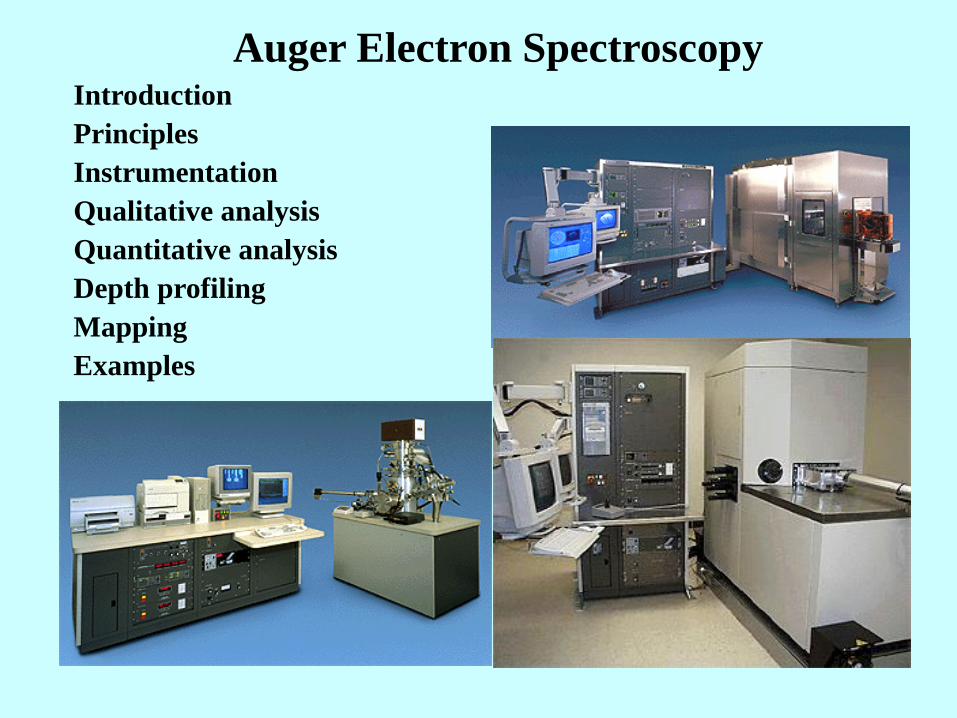
Auger Electron SpectroscopyIntroduction
Principles
Instrumentation
Qualitative analysis
Quantitative analysis
Depth profiling
Mapping
Examples

The Auger Effect is named after its discoverer, Pierre Auger, who
observed a tertiary effect while studying photoemission processes in
the 1920s. Auger electrons are emitted at discrete energies that
allow the atom of origin to be identified. The idea of using
electron-stimulated Auger signals for surface analysis was first
suggested in 1953 by J. J. Lander. The technique became practical
for surface analysis after Larry Harris in 1967 demonstrated the use
of differentiation to enhance the Auger signals.
Pierre Auger
Today Auger electron spectroscopy
is a powerful surface analytical tool
to probe surfaces, thin films, and
interfaces. This utility arises from
the combination of surface
specificity (0.5 to 10 nm), good
spatial surface resolution (as good as
10 nm), periodic table coverage
(except hydrogen and helium), and
reasonable sensitivity (100 ppm for
most elements).
Signals of Auger
electrons
Distribution of Energies of Emitted Electrons
Auger electrons

Electron Beam - Sample Interaction
Primary Electron Beam
Auger Electrons4-50 Å
>Atomic No. 3
Characteristic X-rays> Atomic No. 4
Volume of
Primary
Excitation
<1 - 3 mm
Sample Surface
Backscattered Electrons
Secondary Electrons

Auger Process
The Auger process starts with the removal of an inner shell atomic electron to form a
vacancy. Several processes are capable of producing the vacancy, but bombardment with an
electron beam is the most common. The inner shell vacancy is filled by a second electron
from an outer shell. The energy released kicks a third electron, the Auger electron, out of the
atom.
Auger is a radiationless process. The process of an excited ion decaying into a doubly
charged ion by ejection of an electron is called the Auger process.

N10 4f7/2
N9 4f5/2
N8 4f3/2
N7 4f1/2
N6 4d5/2
N5 4d3/2
N4 4d1/2
N3 4p3/2
N2 4p1/2
N1 4s
M6 3d5/2
M5 3d3/2
M4 3d1/2
M3 3p3/2
M2 3p1/2
M1 3s
L3 2p3/2
L2 2p1/2
L1 2s
K 1s
Nomenclature for Auger Transitions
KL1L2
Transition label
The three symbols in the transition label correspond
to the three energy levels involved in the transition.

Examples of Auger Processes

Auger Electron Spectrum
Electron signal vs electron energy
The Auger peaks are obscure even using an expanded vertical scale.

Electron Energy Spectrum of Pd metal
Direct spectrum
Differential spectrum
- enhances AES features
/ removes background

Plotting d[E N(E)]/dE, of the
above function provides for
clear display of the features in
an Auger electron spectrum.
This d[E N(E)]/dE format is
the most common mode for
presenting Auger data.
Plotting the spectrum as
the differential of the
electron signal, dN(E)/dE,
clarifies some of the
spectral details.

Kinetic EnergiesQualitative analysis depends on the
identification of the elements responsible
for the peaks in the spectrum. The right
figure shows the most useful Auger
peaks in the KLL, LMM, and MNN parts
of the spectrum as well as higher
transitions for elements above cesium.
The red dots indicate the strongest and
most characteristic peaks.
In practice, the
subscripts in the
transition label are
seldom shown.

For an Auger transition ABC, the kinetic
energy of the Auger electron is equal to
EA-EB-EC, where EA, EB, and EC are the
binding energies of electrons in the three
levels. The binding energy of a level in
the presence of a core hole is greater than
the binding energy of the same level in a
neutral atom.
)1()(2
1)1()(
2
1)( zEzEzEzEzEE CCBBAABC
For approximation, the following equation is used to calculate the kinetic
energy of Auger electrons (z: atomic number of the atom).
InitialFinalABC EEE
For exact calculation, other effects should be taken into account, such as
the Coulombic repulsion energy between two holes as well as the intra-
atom and extra atom relaxation energies.
In practice, experimental data are used
for peak identification.
Estimation of Kinetic Energy

Auger Peaks
Auger spectra in the differential distribution characteristic of the
lightest elements (The principal peak is KL2,3L2,3 and the relative
intensities are not plotted to scale)
b)

Auger Peaks
Differentiated Auger spectra
of chromium, manganese, and
iron
Manganese

Chemical InformationThe energy and shape of
an Auger peak contains
information about the
chemical environment.
Theoretical predictions are
difficult and reference
spectra are often used for
comparison.

Auger Electron Intensity X-ray Fluorescence
The Auger process competes with
x-ray fluorescence in an excited
ion.
Auger electron emission is the more
probable decay mechanism for low energy
transitions, i.e., for low atomic number
elements with an initial vacancy in the K
shell and for high atomic number elements
with initial vacancy in the L or M shell.
By choosing an appropriate Auger
transition, all elements (except H and He)
can be detected.

The relative
intensities of
the Auger
electrons also
depend on the
primary
excitation
energy.
The relative
intensities can
be used for
quantitative
analysis
10 keV
electron beam
3 keV
electron beam
KLL
LMM MNN
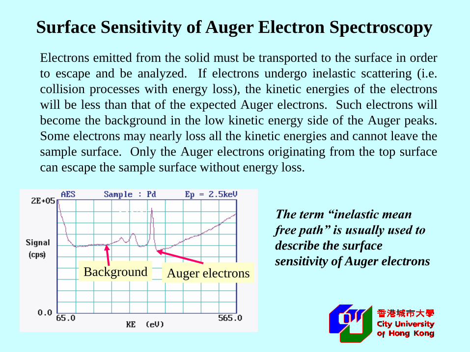
Surface Sensitivity of Auger Electron Spectroscopy
Electrons emitted from the solid must be transported to the surface in order
to escape and be analyzed. If electrons undergo inelastic scattering (i.e.
collision processes with energy loss), the kinetic energies of the electrons
will be less than that of the expected Auger electrons. Such electrons will
become the background in the low kinetic energy side of the Auger peaks.
Some electrons may nearly loss all the kinetic energies and cannot leave the
sample surface. Only the Auger electrons originating from the top surface
can escape the sample surface without energy loss.
Auger electronsBackground
MNN The term “inelastic mean
free path” is usually used to
describe the surface
sensitivity of Auger electrons

Io
Io
Is
Is
de
d
-
=
95.01
1 30
3
0
e
dxe
dxe
x
x
Mean distance that an electron
travels without energy loss
Io: number of electrons originating at a
depth d
Is: number of electrons that can escape
the surface without energy loss
95% of the measured Auger
electrons originate from the depth
region of 3
Inelastic Mean Free Path

Surface Sensitivity of AES
AES spectra of Ni surface: (a) after Ar sputter-cleaning; (b) after
exposure to air for 1 min. showing adsorbed carbon and oxygen.

Instrumentation
Sample
Electron
Source
Electron
energy
analyzer
Ion Gun
Vacuum system
Sample stage
Electronic controls
Computer
Software
Electron
detector

Vacuum System

Sample Handling
Sample introduction
Sample stage with x,
y, z, rotation, and tilt
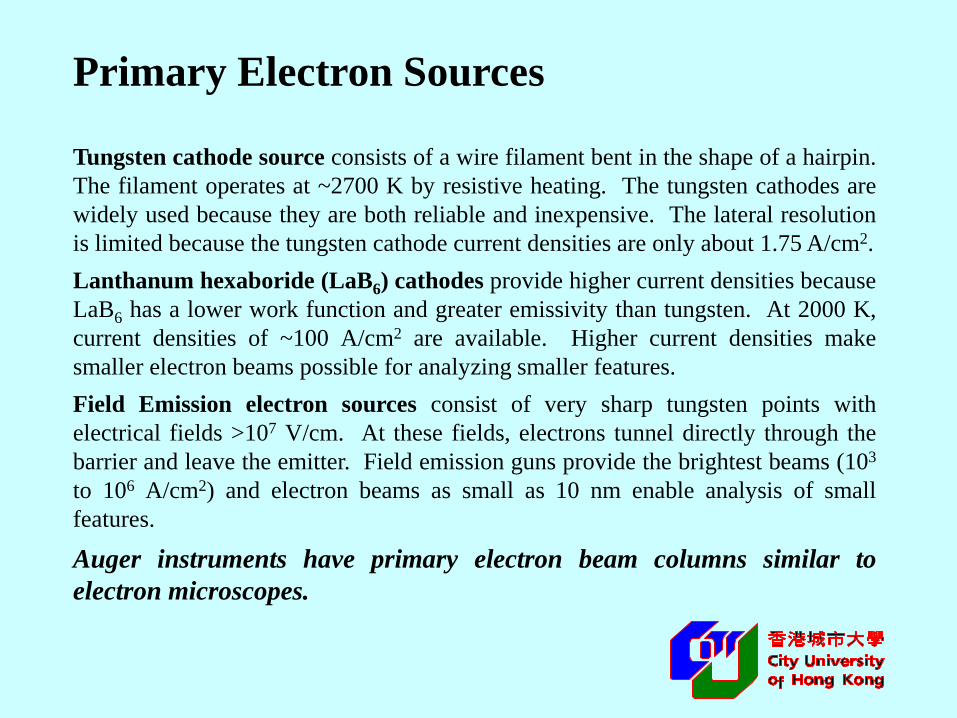
Primary Electron Sources
Tungsten cathode source consists of a wire filament bent in the shape of a hairpin.
The filament operates at ~2700 K by resistive heating. The tungsten cathodes are
widely used because they are both reliable and inexpensive. The lateral resolution
is limited because the tungsten cathode current densities are only about 1.75 A/cm2.
Lanthanum hexaboride (LaB6) cathodes provide higher current densities because
LaB6 has a lower work function and greater emissivity than tungsten. At 2000 K,
current densities of ~100 A/cm2 are available. Higher current densities make
smaller electron beams possible for analyzing smaller features.
Field Emission electron sources consist of very sharp tungsten points with
electrical fields >107 V/cm. At these fields, electrons tunnel directly through the
barrier and leave the emitter. Field emission guns provide the brightest beams (103
to 106 A/cm2) and electron beams as small as 10 nm enable analysis of small
features.
Auger instruments have primary electron beam columns similar to
electron microscopes.

Performance of Field Emission Gun

Electron energy analyzers measure the number of ejected
electrons as a function of the electron energies.
Cylindrical mirror analyzers are most commonly used
because their high transmission efficiency leads to better
signal-to-noise ratios. The primary electron beam hits the
sample surface at the source point of the analyzer. Auger
electrons move outward in all directions and some pass through
the aperture in the inner cylinder. A variable negative potential
on the outer cylinder bends the Auger electrons back through
the second aperture on the inner cylinder and then through an
exit aperture on the analyzer axis.
The energy of the
transmitted electrons is
proportional to the voltage
(-V) on the outer cylinder.
Auger Electron Spectrometer

Electron Detector – Electron Multiplier
An electron multiplier consists of a series of electrodes called dynodes
connected along a resistor string. The output end of the resistor string is
attached to a positive high voltage. The other end of the string goes to the
electron multiplier case and ground. The dynode potentials differ in equal steps
along the chain. When a particle (electron, ion, high energy neutral, or high
energy photon) strikes the first dynode, it produces secondary electrons. The
secondary electrons are accelerated into the next dynode where more secondary
electrons are produced. A cascade of secondary electrons ensues. The dynode
acceleration potential controls the electron gain.

Microchannel Plate Electron Multiplier Arrays
These plates consist of large
arrays of small channel
electron multipliers
Field
Emission
Gun
Microchannel
Plate Detector Cylindrical
Mirror
Analyzer
Sample
Ion beam for sputtering
Electrons at different
energies can be detected
at the same time.

An Ar+ ion beam at kinetic energy 0.5-5 keV is used to bombard the
sample surface to remove surface materials for: (1) surface cleaning, (2)
depth profiling
Ion Gun

Parameters Calibration
Energy scale is calibrated using a flat, fine-grained Cu that has
been sputtered to remove surface oxide and contamination. The
Cu LMM and MNN peaks are measured and the peak positions are
compared to the standard values at 917.8eV and 63.3eV. The
software of most modern AES instruments allows for the
adjustments of the linearity and shifting of the energy scale.
Intensity scale must be calibrated so that the sensitivity factors
measured previously can be used. The instrumental factors
(transmission function and detector efficiency) are measured on
the instrument that gives the sensitivity factors. The instrumental
factors are also measured periodically on the instrument for
adjustment of the sensitivity factors.

Qualitative Analysis
Procedures for Elemental Identification
1. Concentrating on the major peaks and comparing the peak positions
with Auger electron energy chart or table.
2. Referring to the
standard spectra of the
elements in question
and making positive
identification of major
constituents.
3. Labeling all peaks
related to the identified
major constituents.
4. Repeat 1-3 for other
unlabelled peaks.
Auger spectrum of a unknown sample
Primary electron beam energy: 3keV

Ni
Fe
Cr
Ni, Fe and Cr are
preliminarily
identified

Standard spectrum Standard spectrum
Standard spectrum
Fe
CrFe
Ni

N(E) vs E
Peak-to-peak height
Commonly use peak to peak height
of differentiated Auger peak. For
high resolution, use peak area of
the original Auger peak, but this
needs background subtraction.
Peak area
Need background subtraction
Quantitative Analysis
d[EN(E)]/dE vs E
Note: Sensitivities for
these two methods are
different
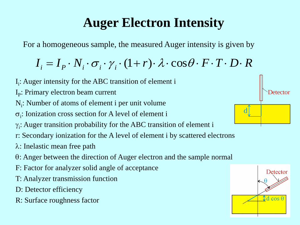
RDTFrNII iiiPi cos)1(
For a homogeneous sample, the measured Auger intensity is given by
Ii: Auger intensity for the ABC transition of element i
IP: Primary electron beam current
Ni: Number of atoms of element i per unit volume
i: Ionization cross section for A level of element i
i: Auger transition probability for the ABC transition of element i
r: Secondary ionization for the A level of element i by scattered electrons
: Inelastic mean free path
: Anger between the direction of Auger electron and the sample normal
F: Factor for analyzer solid angle of acceptance
T: Analyzer transmission function
D: Detector efficiency
R: Surface roughness factor
Auger Electron Intensity
d
Detector

Empirical Approach
Use of relative sensitivity factors (Si)
For two pure elements
22
2
11
1
SN
I
SN
I
The relative sensitivity factors were measured for all elements under a
certain excitation electron beam energy
Ntoi
ii
aa
Ntoi
i
aa
SI
SI
N
NX
11
/
/
Then, the atomic concentration of element a on a sample with N
elements can be determined as
Percentage atomic concentration = Xa100%

The empirical method does not include the matrix effects of the
sample, which includes the inelastic mean free path (), the
backscattering factor (r), and chemical effects on peak shape and
surface roughness. General, an error of 15% is expected using the
empirical method.
For example, a sample reported with 80% Fe and 20% Ni. The error
for Fe could be in the range of 12%.
If standard samples with the same matrix is used for the determination
of the sensitivity factors, the error can be as small as 1%.
Fe
CrFe
NiPeak-to-peak height: Si
Cr peak at 529eV: 4.7 0.32
Fe peak at 703eV: 10.1 0.20
Ni peak at 848eV: 1.5 0.27
Example
%8%;%71%:
%21%10027.0/5.120.0/1.1032.0/7.4
32.0/7.4%
NiFeSimilarly
xCr

Depth Profiling
To analyze samples in depth, Auger instruments incorporate ion
beam sputtering to remove materials from the sample surface
sequentially. One cycle of a typical depth profile consists of
sputtering a small increment into the sample, stopping, measuring
relevant portions of the Auger spectrum, and performing
elemental quantification.
Sputtered
materials
Ar+
Au
ger
sig
nal
Sputtering time
Auger signal can be Auger peak area or peak-to-peak height.

Ion sputtering removes the materials systematically
Auger analysis is performed on the newly exposed crater bottom
and independent of the sputtering process
Auger Depth Profiling

Con
centr
atio
n
Depth
1. Sputtering rate determined from the time required to sputter
through a layer of the same material of known thickness.
2. After the sputtering analysis, the crater depth is measured using
depth profilometry. A constant sputtering rate is assumed.
Au
ger
sig
nal
Sputtering time
Calculation
Calibration of Depth Scale

Pt
Ti
InP
Sample
For each element, an Auger peak is selected at each depth.
Pt: MNN at 1697 eV Ti: LMM at 418 eV
C: KLL at 272 eV In: MNN at 404 eV
O: LMM at 120 eV
Contamination at Semiconductor / Metallization Interface

520Å SiO2
Si
66Å
Depth Resolution Depends on
• Ion beam energy and incident angle
• Surface roughness of sample
• Type of materials
Ar+
Ion
mix
ing
Ion Mixing

Preferential Sputtering
Ar+
Su
rfac
e is
ric
h i
n
8000Å Al
Si
SEM Images
Sputtering time
Poor
depth
resolution
Difference in
• Chemical composition
• Crystal orientation

Sample Rotation
No sample rotation
With sample rotation

Depth Profile of a Ta/Si Multilayer Sample
Depth resolution usually
degrades with depth
Improve depth resolution:
• Sample rotation during Ar+ sputtering
• Low Ar+ energy (less than 1 keV)
• Low incident angle

0 10 20 30 40 50 60 70 80 90 1000
Sputter Time (min)
Inte
nsi
ty
Ti in TiNTi in TiN
NN
Ti in Metallic Ti
O in
SiO2
Si in
SiO2
O in
TiN
Ti in
Oxidized
TiN
0 10 20 30 40 50 60 70 80 90 1000
10
20
30
40
50
60
70
80
90
100
Sputter Time (min)
Ato
mic
Conce
ntr
atio
n (
%)
Ti in TiNTi in TiN
NN
Ti in Metallic Ti
O in
SiO2
Si in
SiO2
O in
TiN
Ti in
Oxidized
TiN
Depth Profiling of TiN/Ti/TiN on SiO2
Two TiN(250Å)/Ti(375Å)/TiN(600Å) on SiO2 samples are analyzed by Auger
depth profiling to determine the film composition and thickness.

Scanning Auger Microscopy
AES Auger Electron Spectroscopy
SAM Scanning Auger Microscopy
Sample
Electron focusing and scanning
Ion Beam
The same instrument can
give SEM images, Auger
spectra and Auger maps.

Gold
Carbon
100 kX SEM
160 kX SEM
Au islands on C
160 kX Auger Maps
Composite Auger image
Secondary electron images

Scanning Auger Microscopy
Images and Auger elemental
maps from a contact pad on a
semiconductor device:
(a) Adsorbed current image;
(b) Secondary electron image;
(c) oxygen map (O KLL, 512
eV);
(d) Silicon oxide map (Si
LMM, 1625 eV, oxide peak);
(e) Silicon map (Si LMM, 1625
eV, non-oxide peak);
(f) aluminum map (Al LMM,
1400 eV).
The Auger maps reveal that the
oxide layer in the middle of the
bond pad has been broken
exposing a small area of
aluminum due to bonding
attempts.
SEM
Sample
current
Auger
Si map
(non-
oxide)
Auger
O map
SEM
Secondary
electrons
Auger
Si map
(oxide)
Auger
Al map

Analysis of bond padTwo chips were supplied for analysis, a chip from a contaminated wafer and
one from a “normal” or good wafer
Secondary Electron Images (Box defines analyzed area for AES)
Bond pad from normal chip Bond pad from contaminated chip

500 1000 1500 2000Kinetic Energy (eV)
dE
xN
(E)/
dE
C
O
F
Al
500 1000 1500 2000Kinetic Energy (eV)
dE
xN
(E)/
dE
C
O
F
Al
Normal Chip
Auger Spectrum of Bond Pad
Contaminated Chip
Auger Spectrum of Bond Pad
Note the difference in F levels
Auger signals acquired from the areas defined in the boxes
Auger electron spectra

SEM/EDX
On DefectSi
O
C
Off Defect
C
Si
Particle found after Si oxy-nitride
deposition and plasma etching
SEM/EDX analysis of a 250 nm particle on a 200 mm Wafer
Comparison of SEM/EDX and SAM

Green = Ti Red = Elemental Si200 400 600 800 1000 1200 1400 1600 1800 2000Kinetic Energy (eV)
Si
Ti O
Si
Spectrum on Particle
Auger spectra from particle
after ~20 nm sputter clean
SAM analysis
of the same
sample

EDS
• Defect: Si and O => Si oxy-nitride
• No Ti found
• Substrate - Si (substrate)
• C observed in both areas - from analysis tool
• Excitation volume too large to study the small particle on
surface
Auger
• Defect: Si, O and Ti
• Ti - contamination from a process tool

SEM/EDX
On Defect
N
Si
Off Defect
N
Si
SEM/EDX analysis of a buried particle

Green = N Red = elemental Si
SAM of the same sample
Sputter to defect (SEM)
As received (SEM)

200 400 600 800 1000 1200 1400 1600 1800 2000Kinetic Energy (eV)
On Exposed ParticleSi
Si
NO
200 400 600 800 1000 1200 1400 1600 1800 2000Kinetic Energy (eV)
Off Exposed ParticleSi
Si
Auger SEM

EDS
• Defect: Si and N
• Substrate: Si and N
• No unique contaminants found
• Excitation volume too large
Auger
• Sputter etched to defect - removing surrounding Si oxy-
nitride layer
• Defect: Si, O, N
• Substrate: Si
• Confirm defect is Si oxy-nitride
AES Summary
• AES uses a focused e-beam to excite Auger electrons
• Auger electrons have energies characteristic of the elements
• Auger electrons - reveal the elemental composition and the
chemistry of the surfaces
• Chemical bonding of the atoms
• Depth profiling in conjunction with ion sputtering
• High spatial resolution of the electron beam and surface
specificity allows for high resolution microanalysis
• AES attributes: high lateral resolution, reasonable sensitivity (100
ppm), semi-quantitative analysis without empirical standards, and
chemical bonding information

AES Characteristics
• Range of elements: All except H and He
• Destructive: No, except to electron beam sensitive materials and during depth
profiling
• Elemental analysis: Yes, semi-quantitative without standards; quantitative with
standards
• Absolute sensitivity: 100 ppm for most elements, depending on the matrix
• Chemical states: Yes, in many materials.
• Depth probed: 0.5- 10 nm (typically 0.5- 3.0 nm).
• Depth profiling: Yes, in concert with ion beam sputtering
• Lateral resolution: 30 nm for AES; even less for SAM imaging
• Imaging/mapping: Yes, Scanning Auger Microscopy (SAM)
• Sample requirements: Vacuum (UHV) compatible materials
• Main use: Elemental composition of inorganic materials
• Instrument cost: US$ 300,000 – 1,000,000

Capabilities of SAM
• Elemental analysis
• Some chemical state information
• Quantification (sensitivity about 0.1 atomic %)
• Small area analysis
• Surface morphology (SEM mode)
• Elemental mapping
• Depth profiling

Sample Tutorial Questions
• How are Auger electrons produced?
• Why is AES surface sensitive?
• How is depth profiling performed?
• Explain the differences between AES and
EDS.
• What kinds of problems are best tackled by
AES?