Embed Size (px)
Citation preview

PHYSICAL REVIEW B 86, 035436 (2012)
Atomic-scale characterization of nitrogen-doped graphite: Effects of dopant nitrogen on the localelectronic structure of the surrounding carbon atoms
Takahiro Kondo,1 Simone Casolo,2 Tetsuya Suzuki,1 Taishi Shikano,1 Masataka Sakurai,1 Yoshihisa Harada,3,4
Makoto Saito,3,* Masaharu Oshima,3,4 Mario Italo Trioni,5 Gian Franco Tantardini,2,5 and Junji Nakamura1,†1Faculty of Pure and Applied Sciences, University of Tsukuba, 1-1-1 Tennodai, Tsukuba, Ibaraki 305-8573, Japan
2Dipartimento di Chimica Fisica ed Elettrochimica, Universita degli Studi di Milano, via Golgi 19, 20133 Milan, Italy3Department of Applied Chemistry, The University of Tokyo, 7-3-1 Bunkyo-ku, Tokyo 113-8656, Japan
4The University of Tokyo Synchrotron Radiation Research Organization, 7-3-1 Bunkyo-ku, Tokyo 113-8656, Japan5CNR National Research Council of Italy, ISTM, via Golgi 19, 20133 Milan, Italy
(Received 4 January 2012; published 23 July 2012)
We report on the local atomic and electronic structures of a nitrogen-doped graphite surface by scanningtunneling microscopy, scanning tunneling spectroscopy, x-ray photoelectron spectroscopy, and first-principlescalculations. The nitrogen-doped graphite was prepared by nitrogen ion bombardment followed by thermalannealing. Two types of nitrogen species were identified at the atomic level: pyridinic-N (N bonded to twoC nearest neighbors) and graphitic-N (N bonded to three C nearest neighbors). Distinct electronic states oflocalized π states were found to appear in the occupied and unoccupied regions near the Fermi level at the carbonatoms around pyridinic-N and graphitic-N species, respectively. The origin of these states is discussed based onexperimental results and theoretical simulations.
DOI: 10.1103/PhysRevB.86.035436 PACS number(s): 81.05.ue, 07.79.Fc, 73.22.Pr, 81.05.uf
I. INTRODUCTION
Nitrogen doping in graphitic materials such as grapheneand carbon nanotubes has been reported to modify physi-cal and chemical properties.1–8 Various applications of N-doped graphite materials have also been reported, suchas in biosensors,9 fuel cells,10–15 capacitors,16 electronicdevices,17–19 and spin filter devices.20,21 By x-ray photoelec-tron spectroscopy (XPS), the nitrogen species in N-dopedgraphite materials12,13,15,19,22–26 have been identified mainly aspyridinic-N (characterized by a binding energy of ∼398.5 eV),pyrrolic-N (400.5 eV), and graphitic-N or quaternary-N(401.2 eV).6,27–29 However, a detailed picture of the localelectronic modifications in N-doped graphite induced by eachof N atoms has not been clarified.
The electronic structure near the Fermi level (EF ) of thegraphite surface is known to be modified by the defect suchas a point vacancy, where localized π electronic states arereported to form at the neighboring C atoms and propagateanisotropically around the defect even to a few nanometersaway from the defect due to the perturbation of the π -conjugated system of graphite.30 It is thus expected that thenitrogen dopants in N-doped graphite modify the electronicstructure near EF and that the modified electronic structureis different from that of the point vacancy defect because thenitrogen bonds to some carbon atoms. It is also expected thatthe modified electronic structure is different depending on thetypes of C-N bonding configurations.
Here, we report on the atomic-scale characterization of aN-doped graphite surface by scanning tunneling microscopy(STM), scanning tunneling spectroscopy (STS), XPS, andfirst-principles calculations based on the density functionaltheory (DFT). Two types of nitrogen species, graphitic-N andpyridinic-N, were identified at the atomic scale, and the effectof each nitrogen species on the local electronic structure of thesurrounding carbon atoms is discussed based on experimentalresults and theoretical simulations.
II. EXPERIMENTAL DETAILS
N-doped graphite was prepared in situ in all experimentsreported here as follows: A fresh highly oriented pyrolyticgraphite (ZYA grade HOPG, Panasonic Inc.) sample wasfirst cleaved in air using an adhesive tape and was placed inan ultra-high-vacuum (UHV) chamber. Subsequently, it wasannealed at 900 ± 50 K. The sample was then bombardedby nitrogen ions of 200 eV (or 500 eV) at 300 K and normalincidence using a commercial ion gun (5-kV ion gun, Anelva).The total ion doses on the sample were set to be lower than 0.2× 10¹³ ions/cm2, which were measured independently usinga Faraday cup (for the XPS experiment, we didn’t measure theion current). After the bombardment, the sample was annealedat 900 ± 50 K for 300 s. Based on the STM observations, theirradiated ions are found to form defects in the sample withhigh efficiency (see, Fig. S1 in the Supplemental Material47).Some nitrogen atoms were implanted into the bulk of thegraphite, and as a result, the STM image showed peculiarcharacteristics, even after further cleavage in air followed byannealing in UHV. The sample temperature during heating wasmeasured using an infrared thermometer.
XPS spectra were measured at 160 K in the UHV chamberwith a base pressure of 3 × 10⁻¹⁰ torr at BL27SU in SPring-8 inHyogo, Japan. The excitation photon energy used in this workwas 700 eV. The x-ray excitation and photoelectron detectionangles were set to 45◦ with respect to the sample normal. Thetotal energy resolution was ∼0.24 eV. Energy calibration wasperformed using the Au 4f7/2 photoemission at 84.0 eV.
STM and STS measurements were performed in the UHVchamber (USM-1200, Unisoku) with a base pressure of 1 ×10⁻¹⁰ torr. A commercial STM controller (SPM-1000, RHKTechnologies) was used. The sample was cooled to 5.3 K.The surface morphology and the surface electronic structurewere then examined by STM and STS, respectively, with aPtIr tip (Pt:Ir = 8:2). STM images were recorded in theconstant-current mode. STS measurements were carried out
035436-11098-0121/2012/86(3)/035436(6) ©2012 American Physical Society
TAKAHIRO KONDO et al. PHYSICAL REVIEW B 86, 035436 (2012)
by measuring the differential conductance (dI /dV ) by alock-in detection technique using 1.0-kHz alternating-currentmodulation of the sample bias voltage with an amplitude of20 mV. dI /dV reflects features in the local density of states(LDOS) of the surface at the position of the STM tip, wheredI /dV at negative and positive sample biases correspond toLDOS of occupied and unoccupied states, respectively, and0 V corresponds to the Fermi level.31 We used a small setcurrent of 50–200 pA to minimize the effect of the tip on thetunneling spectrum. The STS spectra shown here represent theaverage of 10 spectra measured at the same position.
III. THEORETICAL DETAILS
The electronic structure and density of states (DOS) of theN-doped graphite sample were studied using DFT.
In theoretical simulations, an orthorhombic cell was pre-ferred to a hexagonal one to avoid any (fictitious) bandgap due to superlattice effects.32 The supercell was madeby graphene layers of 96 C atoms each, and defects wereintroduced in a single layer or in a three-layer cell, on top ofwhich a 20-A vacuum was used to avoid interaction betweenperiodic replicas. The graphene layers were kept fixed at theexperimental interlayer distance because of the well-knownfailure of DFT in dealing with dispersion forces. After carefultesting, we found that three graphene layers (for a total of 288atoms) are sufficient to obtain converged properties.
Equilibrium geometries for N-doped graphite were firstobtained using a plane wave DFT, as implemented in theVienna ab initio simulation package code,33 by using a 500 eVenergy cutoff and a 3 × 3 × 1 �-centered k-point mesh. Therelaxation of the atomic position was stopped when the highestforce acting on each ion was lower than 0.03 eV/A.
Core electrons, considered frozen here, were includedthrough projector augmented wave potentials,34,35 while small(0.05 eV) Gaussian smearing was used to improve elec-tronic convergence. Exchange and correlation was taken intoaccount according to the gradient-corrected Perdew-Burke-Ernzerhof36 functional. Later, atomic positions were optimizedagain with the Spanish initiative for electronic simulations withthousands of atoms (SIESTA) code37 using a double-ζ pluspolarization basis set, obtaining only negligible differences.
STM images and STS spectra were all simulated usingSIESTA. Accurate LDOS were computed from the electronicground state on a 100 × 100 × 1 k-point mesh, and as STSsimulations, we show the DOS projected on pz orbitals ofthe topmost layer only, which are the ones mainly probed bythe STM tip. The Fermi energy was set to the Dirac point,because this is the limit for diluted defects. Simulated STMimages were obtained within the Tersoff-Hamann approach31
(constant-current mode) for a doped single-layer graphenesystem that was found sufficient to give good agreement withthe experiment. In this work, the spatial distribution of theselected electron densities (obtained from the wave functionsquare modulus) are shown as isosurface plots from a top view.
IV. RESULTS AND DISCUSSION
The XPS and STM measurements of N-doped graphite aredescribed first in Sec. IV A. The local electronic structures
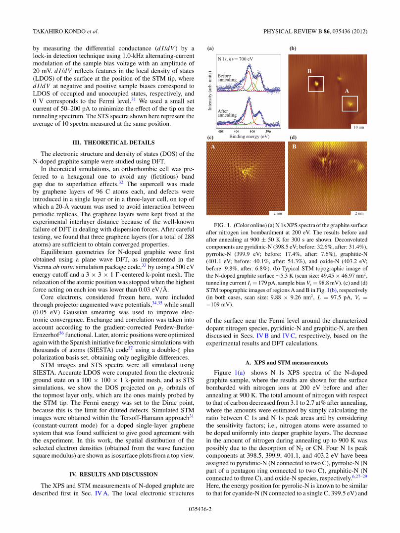
FIG. 1. (Color online) (a) N 1s XPS spectra of the graphite surfaceafter nitrogen ion bombardment at 200 eV. The results before andafter annealing at 900 ± 50 K for 300 s are shown. Deconvolutedcomponents are pyridinic-N (398.5 eV; before: 32.6%, after: 31.4%),pyrrolic-N (399.9 eV; before: 17.4%, after: 7.6%), graphitic-N(401.1 eV; before: 40.1%, after: 54.3%), and oxide-N (403.2 eV;before: 9.8%, after: 6.8%). (b) Typical STM topographic image ofthe N-doped graphite surface ∼5.3 K (scan size: 49.45 × 46.97 nm2,tunneling current It = 179 pA, sample bias Vs = 98.8 mV). (c) and (d)STM topographic images of regions A and B in Fig. 1(b), respectively(in both cases, scan size: 9.88 × 9.26 nm2, It = 97.5 pA, Vs =−109 mV).
of the surface near the Fermi level around the characterizeddopant nitrogen species, pyridinic-N and graphitic-N, are thendiscussed in Secs. IV B and IV C, respectively, based on theexperimental results and DFT calculations.
A. XPS and STM measurements
Figure 1(a) shows N 1s XPS spectra of the N-dopedgraphite sample, where the results are shown for the surfacebombarded with nitrogen ions at 200 eV before and afterannealing at 900 K. The total amount of nitrogen with respectto that of carbon decreased from 3.1 to 2.7 at% after annealing,where the amounts were estimated by simply calculating theratio between C 1s and N 1s peak areas and by consideringthe sensitivity factors; i.e., nitrogen atoms were assumed tobe doped uniformly into deeper graphite layers. The decreasein the amount of nitrogen during annealing up to 900 K waspossibly due to the desorption of N2 or CN. Four N 1s peakcomponents at 398.5, 399.9, 401.1, and 403.2 eV have beenassigned to pyridinic-N (N connected to two C), pyrrolic-N (Npart of a pentagon ring connected to two C), graphitic-N (Nconnected to three C), and oxide-N species, respectively.6,27–29
Here, the energy position for pyrrolic-N is known to be similarto that for cyanide-N (N connected to a single C, 399.5 eV) and
035436-2

ATOMIC-SCALE CHARACTERIZATION OF NITROGEN- . . . PHYSICAL REVIEW B 86, 035436 (2012)
amine-N (N connected to a single C and two H, 399.4 eV),27
possibly also contributing to the same peak. In our samples,pyridinic-N and graphitic-N were the dominant components,as shown in Fig. 1(a). The same two peak components havebeen reported as dominant for nitrogen-doped graphite orgraphene prepared by the ion bombardment method, also fordifferent collision energies (0.1–6.0 keV), different annealingtemperatures, or both.23,25,26,38 However, the ratio of the peakintensities depends on the ion collision energy, flux of ions,and annealing temperature. In Fig. 1(a), graphitic-N is thelargest component (40.1%) after nitrogen ion bombardmentat 200 eV. After annealing to 900 K, the relative intensityof this peak increased (54.3%), suggesting that the otherspecies were converted to graphitic-N. It has been reportedthat the relative amount of pyridinic-N is comparable tothat of graphitic-N when the sample is prepared with higherenergies (a few kiloelectron volts) and more intense ion fluxesof nitrogen.23,25,26,38 This suggests that the graphitic-N-richsurfaces can be obtained with small doses and low energies ofnitrogen ion.
A typical STM image of the N-doped graphite surface isshown in Fig. 1(b). Two types of bright species were observedwith an average diameter of ∼4 nm: one was surrounded bya bright region (type A), and the other was surrounded bya dark region (type B). Because it is generally difficult toidentify surface atom elements by STM alone, we have carriedout the characterization by combining STS analysis and DFTcalculations. We show here that type-A and type-B defects canbe assigned to pyridinic-N species with a single-atom vacancyand graphitic-N species, respectively. These indeed correspondto the two dominant components observed in the XPS spectraof Fig. 1(a). The effect of each dopant N on the local electronicstructure near the Fermi level of the surrounding carbon atomsare discussed later. In Figs. 1(c) and 1(d), some of the brightregions consist of the well-known superstructure of graphiteformed by the standing wave of π electrons around the graphitesurface defects.39,40 In particular, this region does not spreadisotropically around the defect but seems to propagate in threedirections, as observed in the case of a single-atom vacancydefect on a graphite surface.30
B. Pyridinic-N
The experimentally observed STM image and STS spec-trum of a type-A defect are shown in Fig. 2. The STS spectrumshown in Fig. 2(b) was measured at the position indicated bythe arrow in Fig. 2(a), and it consists of a large peak around−370 mV and smaller peaks within a parabolic background.The spectrum is different from that of a single-atom vacancywith a single and large STS peak at41 or just above30,42
the Fermi level. The STS spectrum of the type-A defectis again different from that of the single-atom vacancy ingraphite in terms of a propagation feature.30 That is, themodified electronic states of the single vacancy propagateanisotropically to three directions, while such an anisotropicpropagation was not observed for the type-A defect, as shownin Figs. S6–S8 in the Supplemental Material.47 To identify thedefect species in Fig. 2(a), STM images and STS spectra weresimulated for several types of structures with pyridinic-N orgraphitic-N species because these are the dominant species
(c)
FIG. 2. (Color online) (a) STM topographic image of region Ain Fig. 1(b) (scan size: 4.81 × 4.61 nm2, It = 96.9 pA, Vs =−108 mV). The simulated STM image (V = −0.1 V) is also shownfor comparison. (b) STS spectrum measured at the position indicatedby the arrow in (a). (c) Equilibrium geometry of the pyridinic-N defectcalculated by DFT. (d) Simulated STS spectrum of pyridinic-N.
in our sample, as shown by the XPS peak components inFig. 1(a). After comparison with the results of different defectmodels, we found that the simulated STM and STS features ofpyridinic-N well reproduced those measured in experiments,as shown in Fig. 2; i.e., the propagation of the bright region inSTM and the appearance of the STS peak around −370 mV[Figs. 2(a) and 2(c)] are common between experiment andtheory. The defect was thus assigned as pyridinic-N.
From the DFT calculation, the large STS peak at −370 mVin Figs. 2(b) and 2(d) can be assigned to localized π states (pz
orbitals) because of the localized DOS character (see Fig. S2in the Supplemental Material47). As shown in Fig. 3(a), thespatial propagation of the localized π states can be seen in theSTM simulations at a negative bias of −1.0 V. Most of thebright spots in Fig. 3(a) correspond to the LDOS for the STSpeak at −370 mV (see Fig. S2 in the Supplemental Material47)and are located on few C atoms, part of the same sublatticehosting the N atom.
To further study the electronic structure near the nitrogenatom, the DFT equilibrium geometry and charge densityisosurfaces are examined, as shown in Figs. 3(b) and 3(e). Theisosurface stands for the spatial distribution of orbitals withcertain electron densities, as described in Sec. III. First, thepentagonal ring is found to be formed by the rearrangement ofthe two “edge” carbon atoms facing the nitrogen atom, whichis similar to the case of the C vacancy in graphene.43 Second,the N atom site is imaged as dark in the simulated STM imageat −1.0 V [Fig. 3(a)], even though the nitrogen atom shouldbear one more electron compared to carbon. This is explainedby the occupation of four electrons in the sp2 coplanar orbitalsof N with a lone pair, as can be seen in Figs. 3(c) and 3(f), where
035436-3

TAKAHIRO KONDO et al. PHYSICAL REVIEW B 86, 035436 (2012)
(a) (b) (c)
(d) (e) (f)
FIG. 3. (Color online) Simulated STM images (constant-currentmode) for the pyridinic-N graphene defect: (a) V = −1.0 V and(d) V = +1.0 V. The N atom is placed at the center of the image.(b) DFT equilibrium geometry and isosurface plot of electron densityat 1.5 × 10⁻³ electrons/A3 integrated from −0.7 eV to the Fermi level(square modulus of the wave function up to the Fermi level from −0.7eV). The N atom is shown in light gray. (c) Same image as Fig. 3(b)except for color near the nitrogen atom, where only the xy-planeDOS contribution near N is represented by blue–red gradients.(e) DFT equilibrium geometry and isosurface plot of electron densityat 1.5 × 10⁻³ electrons/A3 integrated from the Fermi level to +0.7eV. (f) Schematic representation of pz orbitals in pyridinic-N.
the in-plane contribution to the electron density is representedby blue–red gradients.
Here, we discuss the appearance of the localized states in theoccupied region. The formation of the lone pair suggests thatthe N atom of the pyridinic defect is negatively charged. Thenegatively charged N is consistent with the chemical shift in N1s binding energy to lower energy for pyridinic-N (398.5 eV) inthe XPS spectrum compared to that for graphitic-N (401.1 eV).If N is negatively charged, the surrounding carbon atoms wouldbe charged positively because of the screening effect. Thepositive charge of carbon can explain a shift of the localizedπ state of carbon from the Fermi level to the lower (deeper)energy level. Following this picture, we suggest that the statescorresponding to the STS peak in the occupied region near theFermi level may act as a Lewis base toward molecular species.
At positive bias, i.e., for the unoccupied region, theisosurface plot in Fig. 3(e) shows a nodal plane across thepentagon, suggesting the antibonding character of the stateslying above the pentagon ring. A slightly long-range propa-gating feature can be observed in the simulated STM imageof Fig. 3(d), suggesting the appearance of localized states.There is, however, no distinct sharp peak in the simulatedSTS spectrum in the energy range from 0 to +1.0 eV. Thepropagation can thus be explained by the presence of weaklylocalized π states, where the localization is much weakercompared to the occupied region, as shown by the isosurfaceplot in Fig. 3(e). The feature of threefold propagation inFig. 3(e) is similar to the case of a single-atom vacancy in
FIG. 4. (Color online) (a) STM topographic image correspondingto the defect shown in region B in Fig. 1(b) (image taken from adifferent sample, scan size: 5.09 × 5.08 nm2, It = 39.0 pA, Vs =500 mV). The simulated STM image (V = +0.5 V) is also shown forcomparison. (b) STS spectrum measured at the position indicated bythe arrow in (a). (c) Equilibrium geometry of the graphitic-N defectcalculated by DFT. (d) Simulated STS spectrum of graphitic-N.
graphite,30,41–44 though the localization is much weaker forpyridinic-N.
C. Graphitic-N
The experimentally observed STM image at +500 mV andSTS spectrum of a type-B defect are shown in Fig. 4. The STSis different from that for the pristine graphite in terms of theasymmetric LDOS with respect to 0 V (the Fermi level), wherelarger intensity can be recognized in the positive bias region(unoccupied region). The small shoulder peak can be seen atthe positive bias voltage, which is in contrast to that at thenegative voltage observed for pyridinic-N. The STS spectrawith the same shape have been measured in the vicinity ofthe defect independent of the lateral position, as measuredin pyridinic-N (see Figs. S9–S1447). To identify the defectspecies in Fig. 4(a), DFT simulations of STM images andSTS spectra were carried out assuming several types of defectstructures. After comparison with the results of different defectmodels, we found that the simulated STM and STS features ofgraphitic-N well reproduced those measured in experiments,as shown in Figs. 4 and S3. That is, triangular bright spotsin the STM image and the STS peak (enhanced intensity)around +500 mV are common between experiment and theory.The defect was thus assigned as graphitic-N. In the DFTcalculation, the position of the N atom in graphitic-N speciesis almost the same as that of the C atom in graphite (shorter by0.002 nm for the CN bond length than for the CC bond length).That is, the nitrogen species takes the sp2 planar structure ofgraphite. Concerning the origin of the STS peak at 500 mV,the state is ascribed to localized π states (pz orbitals), which
035436-4

ATOMIC-SCALE CHARACTERIZATION OF NITROGEN- . . . PHYSICAL REVIEW B 86, 035436 (2012)
FIG. 5. (Color online) Simulated STM images of the graphitic-Ndefect: (a) V = −0.5 V, and (c) V = +0.5 V. The N atom is placed atthe center of the image. DFT equilibrium geometry and isosurface plotof electron (b) electron density at 2 × 10⁻⁴ electrons/A3 integratedfrom −0.7 eV to the Fermi level (square modulus of wave functionup to the Fermi level from −0.7 eV) and (d) electron density at 1.5 ×10⁻³ electrons/A3 integrated from the Fermi level to +0.7 eV.
is similar to the edge state because of the localized character(see Fig. S3 in the Supplemental Material47). In the simulatedSTM image (Fig. 5), the bright triangular spots are due to theenhanced LDOS component around +500 mV. In addition,15–20 carbon atoms are imaged bright, indicating that thelocalized π states propagate near the defect. As shown inFigs. S4 and S5,47 the N atom position in Fig. 4(a) is found asthe substituted position of a β-carbon atom (C atoms locatedabove the center of a hexagonal ring; the remaining C atomsare called α-carbon atoms45).
Here, we discuss the appearance of the localized states inthe unoccupied region. The positively charged N is expected bythe chemical shift in N 1s binding energy to higher energy forgraphitic-N (401.1 eV) in the XPS spectrum compared to thatfor pyridinic-N (398.5 eV). Indeed, the difference of 2.6 eVis so large that the binding energy of 401.1 eV is comparablewith that for the pyridinium ion, C5H5NH+ (401.2 eV), andthe ammonium ion, NH+
4 (401.5 eV), where N is positivelycharged in both cases,27 suggesting a positive charge for N ofgraphitic-N. The positively charged N of graphitic-N has alsobeen reported recently based on theoretical results by Yu et al.8
and Meyer et al.46 The positive charge can be explained byelectron transfer from the N atom to the π conjugated state. IfN is positively charged, the surrounding carbon atoms shouldbe charged negatively because of the screening effect. Thenegative charge of carbon can explain a shift of the localizedπ state of carbon from the Fermi level to the upper energy level.
In addition, the screening of the positive N charge may be thesource of the dark halo around the graphitic-N defect seen inFigs. 1(b) and 1(d); i.e., the charge density rearrangement maybe induced by the positive charge of N, and it may cause themodulated contrast in the STM image around the N atom. Here,the states with the STS peak in the unoccupied region near theFermi level may act as a Lewis acid. The STS peak position ofgraphitic-N should depend on the amount of doped nitrogen.The amount of electron doping (n) due to N impurities per unitarea in a single graphene layer can be approximately quantifiedby the integral of the new (shifted) Fermi surface (FS) at agiven energy (E) away from the pristine Fermi level. This, forindependent electrons, is represented as
n = 4
4π2
∮FS
dk = |k|2π
= E2
h2πv2F
(1)
in which we included the factor 4 to account for spin andvalley degeneracy and where the linear band dispersion ofgraphene E = h vF |k| was used. Then, the shift in the Fermienergy should scale as E = h vF (πn)1/2, where νF is theFermi velocity (∼106 m s−1). Following these arguments, itmay be possible to control the population of the defect statesby controlling the N concentration. For low N doses (verysmall n), the extra electron introduced by the impurity intothe graphene layer would cause infinitely small doping, thusinducing a positive charge on the N atom. Otherwise, for highdoses, the doping would be sufficient to doubly occupy the pz
orbital (i.e., the states responsible for the STS peak at +500mV), giving rise to a neutral defect. From Eq. (1), we estimatedthat a concentration of more than 1.8 × 10¹³ defects/cm2
(∼1 graphitic-N for every 210 carbon atoms in the singlegraphene layer) should be sufficient to raise the Fermi energyby ∼0.5 eV where these states occur.
V. CONCLUSIONS
We have examined a N-doped graphite surface by STM,STS, XPS, and first-principles calculations. Two types ofnitrogen species have been identified on the N-doped graphitesurface: pyridinic-N with single-atom vacancy and graphitic-N. While pyridinic-N defects induce an atomic rearrangementto form a pentagon, graphitic-N affects the structure onlyslightly. In each case, the electronic structure of graphiteclose to the Fermi energy is found to be modified by thedefects. The distinct localized π states appear in occupied andunoccupied regions near the Fermi level around pyridinic-Nand graphitic-N species, respectively.
ACKNOWLEDGMENTS
This work was financially supported by the New Energy andIndustrial Technology Development Organization of Japan.We acknowledge CINECA consortium for computationalresources and Rocco Martinazzo for fruitful discussions.
035436-5

TAKAHIRO KONDO et al. PHYSICAL REVIEW B 86, 035436 (2012)
*Present address: Toyota Motor. Corporation, 1200, Mishuku,Susono, Shizuoka, 410-11 Japan.
†Corresponding author: [email protected]. Deifallah, P. F. McMillan, and F. Cora, J. Phys. Chem. C 112,5447 (2008).
2N. M. R. Peres, F. Guinea, and A. H. CastroNeto, Phys. Rev. B 72,174406 (2005).
3S. Stafstrom, Appl. Phys. Lett. 77, 3941 (2000).4A. A. Thomas, A. Fischer, F. Goettmann, M. Antonietti, J. O.Muller, R. Schlogl, and J. M. Carlsson, J. Mater. Chem. 18, 4893(2008).
5S. S. Yu, W. T. Zheng, Q. B. Wen, and Q. Jiang, Carbon 46, 537(2008).
6S. Maldonado, S. Morin, and K. J. Stevenson, Carbon 44, 1429(2006).
7T. Kondo, T. Suzuki, and J. Nakamura, J. Phys. Chem. Lett. 2, 577(2011).
8S.-S. Yu and W.-T. Zheng, Nanoscale 2, 1069 (2010).9Y. Wang, Y. Shao, D. W. Matson, J. Li, and Y. Lin, ACS Nano 4,1790 (2010).
10L. Qu, Y. Liu, J.-B. Baek, and L. Dai, ACS Nano 4, 1321(2010).
11S. F. Huang, K. Terakura, T. Ozaki, T. Ikeda, M. Boero, M. Oshima,J. I. Ozaki, and S. Miyata, Phys. Rev. B 80, 235410 (2009).
12C. V. Rao, C. R. Cabrera, and Y. Ishikawa, J. Phys. Chem. Lett. 1,2622 (2010).
13Y. Zhou, J. Mater. Chem. 19, 7830 (2009).14R. A. Sidik, A. B. Anderson, N. P. Subramanian, S. P. Kumaraguru,
and B. N. Popov, J. Phys. Chem. B 110, 1787 (2006).15D. H. Lee, W. J. Lee, W. J. Lee, S. O. Kim, and Y.-H. Kim, Phys.
Rev. Lett. 106, 175502 (2011).16H. M. Jeong, J. W. Lee, W. H. Shin, Y. J. Choi, H. J. Shin, J. K.
Kang, and J. W. Choi, Nano Lett. 11, 2472 (2011).17X. Wang, X. Li, L. Zhang, Y. Yoon, P. K. Weber, H. Wang, J. Guo,
and H. Dai, Science 324, 768 (2009).18R. A. Nistor, D. M. Newns, and G. J. Martyna, ACS Nano 5, 3096
(2011).19D. Wei, Y. Liu, Y. Wang, H. Zhang, L. Haung, and G. Yu, Nano
Lett. 9, 1752 (2009).20Y. Li, Z. Zhou, P. Shen, and Z. Chen, ACS Nano 3, 1952 (2009).21B. Biel, X. Blase, F. Triozon, and S. Roche, Phys. Rev. Lett. 102,
096803 (2009).22G. Imamura and K. Saiki, J. Phys. Chem. C 115, 10000 (2011).23K.-J. Kim, H. Lee, J. Choi, H. Lee, M. C. Jung, H. J. Shin, T. H.
Kang, B. Kim, and S. Kim, J. Phys. Condens. Matter 22, 045005(2010).
24D. Deng, X. Pan, L. Yu, Y. Cui, Y. Jiang, J. Qi, W. Li, Q. Fu,X. Ma, Q. Xue, G. Sun, and X. Bao, Chem. Mater. 23, 1188 (2011).
25D.-Q. Yang and E. A. Sacher, Surf. Sci. 531, 185 (2003).26I. Kusunoki, M. Sakai, Y. Igari, S. Ishidzuka, T. Takami, T. Takaoka,
M. N. Gamo, and T. Ando, Surf. Sci. 492, 315 (2001).27J. R. Pels, F. Kapteijn, J. A. Moulijn, Q. Zhu, and K. M. Thomas,
Carbon 33, 1641 (1995).28E. Raymundo-Pinero, D. Cazorla-Amoros, A. Linares-Solano,
J. Find, U. Wild, and R. Schlogl, Carbon 40, 597 (2002).29R. Arrigo, M. Havecker, S. Wrabetz, R. Blume, M. Lerch,
J. McGregor, E. Parrott, J. Zeitler, L. Gladden, A. Knop-Gericke,R. Schlogl, and D. S. Su, J. Am. Chem. Soc. 132, 9616(2010).
30T. Kondo, Y. Honma, J. Oh, T. Machida, and J. Nakamura, Phys.Rev. B 82, 153414 (2010).
31J. Tersoff and D. R. Hamann, Phys. Rev. B 31, 805 (1985).32S. Casolo, R. Martinazzo, and G. F. Tantardini, J. Phys. Chem. C
115, 3250 (2011).33G. Kresse and J. Furthmuller, Comput. Mat. Sci. 6, 15 (1996).34P. E. Blochl, Phys. Rev. B 50, 17953 (1994).35G. Kresse and D. Joubert, Phys. Rev. B 59, 1758 (1999).36J. P. Perdew, K. Burke, and M. Ernzerhof, Phys. Rev. Lett. 77, 3865
(1996).37J. M. Soler, E. Artacho, J. D. Gale, A. Garcıa, J. Junquera,
P. Ordejon, and D. Sanchez-Portal, J. Phys. Condens. Matter 14,2745 (2002).
38D.-Q. Yang and E. Sacher, App. Surf. Sci. 195, 202 (2002).39P. Ruffieux, M. Melle-Franco, O. Groning, M. Bielmann,
F. Zerbetto, and P. Groning, Phys. Rev. B 71, 153403 (2005).40H. A. Mizes and J. S. Foster, Science 244, 559 (1989).41M. M. Ugeda, I. Brihuega, F. Guinea, and J. M. Gomez-Rodriguez,
Phys. Rev. Lett. 104, 096804 (2010).42J. Oh, T. Kondo, D. Hatake, Y. Honma, K. Arakawa, T. Machida,
and J. Nakamura, J. Phys. Condens. Matter 22, 304008 (2010).43Y. Ma, P. O. Lehtinen, A. S. Foster, and R. M. Nieminen, New J.
Phys. 6, 68 (2004).44R. Martinazzo, S. Casolo, and G. F. Tantardini, in Physics and
Applications of Graphene—Theory, edited by S. Mikhailov (Intech,Rijeka, 2011), Chap. 3, pp. 45.
45D. Tomanek, S. G. Louie, H. J. Mamin, D. W. Abraham, R. E.Thomson, E. Ganz, and J. Clarke, Phys. Rev. B 35, 7790 (1987).
46J. C. Meyer, S. Kurasch, H. J. Park, V. Skakalova, D. Kuenzel,A. Gross, A. Chuvilin, G. Algara-Siller, S. Roth, T. Iwasaki,U. Starke, J. H. Smet, and U. Kaiser, Nat. Mater. 10, 209 (2011).
47See Supplemental Material at http://link.aps.org/supplemental/10.1103/PhysRevB.86.035436 for efficiency of N-doping, effectof the sample bias on the STM images, analysis and effect of Natom position, STS around defect of nitrogen doped graphite andexample of the characterization of N species on N-doped graphitebased on the current work.
035436-6