Embed Size (px)
Citation preview

DS-25SL128–090A–4/2016
Features
Single 1.65V - 1.95V Supply
Serial Peripheral Interface (SPI) and Quad Peripheral Interface (QPI) Compatible Supports SPI Modes 0 and 3 Supports Dual and Quad Output Read Supports QPI Output Read
104 MHz Maximum Operating Frequency Clock-to-Output (tV) of 7 ns
Full Chip Erase
Flexible, Optimized Erase Architecture for Code and Data Storage Applications 0.7 ms Typical Page Program (256 Bytes) Time 60 ms Typical 4-Kbyte Block Erase Time 200 ms Typical 32-Kbyte Block Erase Time 400 ms Typical 64-Kbyte Block Erase Time
Hardware Controlled Locking of Protected Blocks via WP Pin
HOLD or RESET Pin Option
Software and Hardware Write Protection
Three Protected Programmable Security Register Pages
Serial Flash Discoverable Parameters (SFDP) Register
Flexible Programming Byte/Page Program (1 to 256 Bytes) Quad Input Byte/Page Program (1 to 256 Bytes)
Erase Suspend and Resume
JEDEC Standard Manufacturer and Device ID Read Methodology
Low Power Dissipation 4µA Deep Power-Down Current (Typical) 40µA Standby current (Typical) 6mA Active Read Current (Typical)
Endurance: 100,000 program/erase cycles
Data Retention: 20 Years
Industrial Temperature Range: -40°C to +85°C
Industry Standard Green (Pb/Halide-free/RoHS Compliant) Package Options 8-lead SOIC (208-mil) 8-pad Ultra Thin DFN (6 x 5 x 0.8 mm) 9-ball Ultra Thin Ball Grid Array (UBGA) 21-ball die Ball Grid Array (dBGA - WLCSP) Die in Wafer Form
AT25SL128
128-Mbit, 1.65V Minimum SPI Serial Flash Memory with Dual I/O, Quad I/O and QPI Support
ADVANCE DATASHEET

2AT25SL128 DS-25SL128–090A–4/2016
1. IntroductionThe Adesto® AT25SL128 is a serial interface Flash memory device designed for use in a wide variety of high-volume consumer based applications in which program code is shadowed from Flash memory into embedded or external RAM for execution. The flexible erase architecture of the AT25SL128 is ideal for data storage as well, eliminating the need for additional data storage devices.
The erase block sizes of the AT25SL128 have been optimized to meet the needs of today's code and data storage applications. By optimizing the size of the erase blocks, the memory space can be used much more efficiently. Because certain code modules and data storage segments must reside by themselves in their own erase regions, the wasted and unused memory space that occurs with large block erase Flash memory devices can be greatly reduced. This increased memory space efficiency allows additional code routines and data storage segments to be added while still maintaining the same overall device density.
The device also contains three pages of Security Register that can be used for purposes such as unique device serialization, system-level Electronic Serial Number (ESN) storage, locked key storage, etc. These Security Register pages can be individually locked.
The following figures show the available package types.
Figure 1-1. 8-SOIC (Top View) Figure 1-2. 8-UDFN (Top View)
Figure 1-3. 9-ball UBGA (Top View) Figure 1-4. 21-WLCSP (Bottom View)
1234
8765
CSSOWP
GND
VCCHOLDSCKSI
CSSOWP
GND
1
2
3
4
8
7
6
5
VCCHOLDSCKSI
SCK GND VCC
WPNCCS
SO SI HOLD
NC
NC
NC
NC
NC NC
NC
NC
NC
NC
NC
NC
NC
GND I/O0(SI)
SCK
I/O1(SO)
Vcc
I/O3(HOLD)
I/O2(WP)
CS

3AT25SL128 DS-25SL128–090A–4/2016
2. Pin Descriptions and Pinouts
During all operations, VCC must be held stable and within the specified valid range: VCC (min) to VCC (max).
All of the input and output signals must be held high or low (according to voltages of VIH, VOH, VIL or VOL.
Table 2-1. Pin Descriptions
Symbol Name and FunctionAsserted
State Type
CS
CHIP SELECT
Asserting the CS pin selects the device. When the CS pin is deasserted, the device is deselected and normally placed in standby mode (not Deep Power-Down mode). The SO pin is placed in a high-impedance state. When the device is deselected, data is not accepted on the SI pin.A high-to-low transition on the CS pin is required to start an operation, and a low-to-high transition is required to end an operation. When ending an internally self-timed operation such as a program or erase cycle, the device does not enter the standby mode until the completion of the operation.
Low Input
SCK
SERIAL CLOCK
This pin is used to provide a clock to the device and is used to control the flow of data to and from the device. Command, address, and input data present on the SI pin is always latched in on the rising edge of SCK, while output data on the SO pin is always clocked out on the falling edge of SCK.
- Input
SI (I/O0)
SERIAL INPUT
The SI pin is used to shift data into the device. The SI pin is used for all data input including command and address sequences. Data on the SI pin is always latched in on the rising edge of SCK.
With the Dual-Output and Quad-Output Read commands, the SI Pin becomes an output pin (I/O0) in conjunction with other pins to allow two or four bits of data on (I/O3-0) to be clocked in on every falling edge of SCK
To maintain consistency with the SPI nomenclature, the SI (I/O0) pin is referenced as the SI pin unless specifically addressing the Dual-I/O and Quad-I/O modes in which case it is referenced as I/O0.
Data present on the SI pin is ignored whenever the device is deselected (CS is deasserted).
- Input/Output
SO (I/O1)
SERIAL OUTPUT
The SO pin is used to shift data out from the device. Data on the SO pin is always clocked out on the falling edge of SCK.
With the Dual-Output Read commands, the SO Pin remains an output pin (I/O0) in conjunction with other pins to allow two bits of data on (I/O1-0) to be clocked in on every falling edge of SCK
To maintain consistency with the SPI nomenclature, the SO (I/O1) pin is referenced as the SO pin unless specifically addressing the Dual-I/O modes in which case it is referenced as I/O1.
The SO pin is in a high-impedance state whenever the device is deselected (CS is deasserted).
- Input/Output

4AT25SL128 DS-25SL128–090A–4/2016
WP (I/O2)
WRITE PROTECT
The WP pin controls the hardware locking feature of the device.
With the Quad-Input Byte/Page Program command, the WP pin becomes an input pin (I/O2) and, along with other pins, allows four bits (on I/O3-0) of data to be clocked in on every rising edge of SCK. With the Quad-Output Read commands, the WP Pin becomes an output pin (I/O2) in conjunction with other pins to allow four bits of data on (I/O33-0) to be clocked in on every falling edge of SCK.
To maintain consistency with the SPI nomenclature, the WP (I/O2) pin is referenced as the WP pin unless specifically addressing the Quad-I/O modes in which case it is referenced as I/O2.
The WP pin is internally pulled-high and may be left floating if hardware controlled protection is not used. However, it is recommended that the WP pin also be externally connected to VCC whenever possible.
If WP is driven Low while the Status Register Protect bits (SRP1 and SRP0) of the Status Registers are set to 0 and 1 respectively, it is not possible to write to the Status Registers. This is done to prevent any alteration of the Status Registers. As a consequence, all the data bytes in the memory area that are protected by the Block Protect, TB, SEC bits in the status registers, are also hardware protected against data modification while WP remains Low. Note that the WP pin functionality is not available when Quad or QPI mode is enabled (QE).
- Input/Output
Table 2-1. Pin Descriptions (Continued)
Symbol Name and FunctionAsserted
State Type

5AT25SL128 DS-25SL128–090A–4/2016
RESET
HOLD (I/O3)
HOLD
The HOLD pin is used to temporarily pause serial communication without deselecting or resetting the device. While the HOLD pin is asserted, transitions on the SCK pin and data on the SI pin are ignored and the SO pin is placed in a high-impedance state.
The CS pin must be asserted, and the SCK pin must be in the low state in order for a Hold condition to start. A Hold condition pauses serial communication only and does not have an effect on internally self-timed operations such as a program or erase cycle.
With the Quad-Input Byte/Page Program command, the HOLD pin becomes an input pin (I/O3) and, along with other pins, allows four bits (on I/O3-0) of data to be clocked in on every rising edge of SCK. With the Quad-Output Read commands, the HOLD Pin becomes an output pin (I/O3) in conjunction with other pins to allow four bits of data on (I/O33-0) to be clocked in on every falling edge of SCK.
To maintain consistency with the SPI nomenclature, the HOLD (I/O3) pin is referenced as the HOLD pin unless specifically addressing the Quad-I/O modes in which case it is referenced as I/O3.
The HOLD pin is internally pulled-high and may be left floating if the Hold function is not used. However, it is recommended that the HOLD pin also be externally connected to VCC whenever possible.
When the QE bit in the Status register is cleared, the IO3 pin can be configured either as a HOLD pin or as a RESET pin depending on the state of the HOLD/RESET bit 7 in Status Register 3. Note that when the QE bit is set, the HOLD or RESET function is not available as this pin is used to transfer data.
- Input/Output
VCC
DEVICE POWER SUPPLY: VCC is the supply voltage. It is the single voltage used for all device functions including read, program, and erase.
The VCC pin is used to supply the source voltage to the device.
Operations at invalid VCC voltages may produce spurious results and should not be attempted.
- Power
GND
GROUND: VSS is the reference for the VCC supply voltage.
The ground reference for the power supply. GND should be connected to the system ground.
- Power
Table 2-1. Pin Descriptions (Continued)
Symbol Name and FunctionAsserted
State Type

6AT25SL128 DS-25SL128–090A–4/2016
3. Block Diagram
Figure 3-1 shows a block diagram of the AT25SL128 serial Flash.
Figure 3-1. AT25SL128 Block Diagram
FlashMemory
Array
Y-Gating
CS
SCK
Note: I/O3-0 pin naming convention is used for Dual-I/O and Quad-I/O commands.
SO (I/O1)
SI (I/O0)Y-Decoder
Add
ress
Lat
ch
X-Decoder
I/O Buffersand Latches
Control andProtection Logic
SRAMData Buffer
WP (I/O2)
InterfaceControl
AndLogic
HOLD (I/O3)
RESET or

7AT25SL128 DS-25SL128–090A–4/2016
4. Memory Array
To provide the greatest flexibility, the memory array of the AT25SL128 can be erased in four levels of granularity including a full chip erase. The size of the erase blocks is optimized for both code and data storage applications, allowing both code and data segments to reside in their own erase regions. The Memory Architecture Diagram illustrates the breakdown of each erase level.
Figure 4-1. Memory Architecture Diagram
64KB 32KB 4KB 1-256 Byte
4KB FFFFFFh – FFF000h 256 Bytes FFFFFFh – FFFF00h4KB FFEFFFh – FFE000h 256 Bytes FFFEFFh – FFFE00h4KB FFDFFFh – FFD000h 256 Bytes FFFDFFh - FFFD00h4KB FFCFFFh – FFC000h 256 Bytes FFFCFFh – FFFC00h4KB FFBFFFh – FFB000h 256 Bytes FFFBFFh – FFFB00h4KB FFAFFFh – FFA000h 256 Bytes FFFAFFh – FFFA00h4KB FF9FFFh – FF9000h 256 Bytes FFF9FFh – FFF900h4KB FF8FFFh – FF8000h 256 Bytes FFF8FFh – FFF800h4KB FF7FFFh – FF7000h 256 Bytes FFF7FFh – FFF700h4KB FF6FFFh – FF6000h 256 Bytes FFF6FFh – FFF600h4KB FF5FFFh – FF5000h 256 Bytes FFF5FFh – FFF500h4KB FF4FFFh – FF4000h 256 Bytes FFF4FFh – FFF400h4KB FF3FFFh – FF3000h 256 Bytes FFF3FFh – FFF300h4KB FF2FFFh – FF2000h 256 Bytes FFF2FFh – FFF200h4KB FF1FFFh – FF1000h 256 Bytes FFF1FFh – FFF100h4KB FF0FFFh – FF0000h 256 Bytes FFF0FFh – FFF000h4KB FEFFFFh – FEF000h 256 Bytes FFEFFFh – FFEF00h4KB FEEFFFh – FEE000h 256 Bytes FFEEFFh – FFEE00h4KB FEDFFFh – FED000h 256 Bytes FFEDFFh – FFED00h4KB FECFFFh – FEC000h 256 Bytes FFECFFh – FFEC00h4KB FEBFFFh – FEB000h 256 Bytes FFEBFFh – FFEB00h4KB FEAFFFh – FEA000h 256 Bytes FFEAFFh – FFEA00h4KB FE9FFFh – FE9000h 256 Bytes FFE9FFh – FFE900h4KB FE8FFFh – FE8000h 256 Bytes FFE8FFh – FFE800h4KB FE7FFFh – FE7000h4KB FE6FFFh – FE6000h4KB FE5FFFh – FE5000h4KB FE4FFFh – FE4000h 256 Bytes 0017FFh – 001700h4KB FE3FFFh – FE3000h 256 Bytes 0016FFh – 001600h4KB FE2FFFh – FE2000h 256 Bytes 0015FFh – 001500h4KB FE1FFFh – FE1000h 256 Bytes 0014FFh – 001400h4KB FE0FFFh – FE0000h 256 Bytes 0013FFh – 001300h
256 Bytes 0012FFh – 001200h256 Bytes 0011FFh – 001100h256 Bytes 0010FFh – 001000h
4KB 00FFFFh – 00F000h 256 Bytes 000FFFh – 000F00h4KB 00EFFFh – 00E000h 256 Bytes 000EFFh – 000E00h4KB 00DFFFh – 00D000h 256 Bytes 000DFFh – 000D00h4KB 00CFFFh – 00C000h 256 Bytes 000CFFh – 000C00h4KB 00BFFFh – 00B000h 256 Bytes 000BFFh – 000B00h4KB 00AFFFh – 00A000h 256 Bytes 000AFFh – 000A00h4KB 009FFFh – 009000h 256 Bytes 0009FFh – 000900h4KB 008FFFh – 008000h 256 Bytes 0008FFh – 000800h4KB 007FFFh – 007000h 256 Bytes 0007FFh – 000700h4KB 006FFFh – 006000h 256 Bytes 0006FFh – 000600h4KB 005FFFh – 005000h 256 Bytes 0005FFh – 000500h4KB 004FFFh – 004000h 256 Bytes 0004FFh – 000400h4KB 003FFFh – 003000h 256 Bytes 0003FFh – 000300h4KB 002FFFh – 002000h 256 Bytes 0002FFh – 000200h4KB 001FFFh – 001000h 256 Bytes 0001FFh – 000100h4KB 000FFFh – 000000h 256 Bytes 0000FFh – 000000h
• • •
Sector 0
Block Erase Detail Page Program DetailPage AddressBlock Address
Block509
Block508
Range
• • •
• • •
Range
Block0
Block1
• • •
Sector 255
Block 511
Block510
Sector 254

8AT25SL128 DS-25SL128–090A–4/2016
5. Device Operation
The AT25SL128 is controlled by a set of commands that are sent from a host controller, commonly referred to as the SPI Master. The SPI Master communicates with the AT25SL128 via the SPI bus which is comprised of four signal lines: Chip Select (CS), Serial Clock (SCK), Serial Input (SI), and Serial Output (SO).
The SPI protocol defines a total of four modes of operation (mode 0, 1, 2, or 3) with each mode differing in respect to the SCK polarity and phase and how the polarity and phase control the flow of data on the SPI bus. The AT25SL128 supports the two most common modes, SPI Modes 0 and 3. The only difference between SPI Modes 0 and 3 is the polarity of the SCK signal when in the inactive state (when the SPI Master is in standby mode and not transferring any data). With SPI Modes 0 and 3, data is always latched in on the rising edge of SCK and always output on the falling edge of SCK.
Figure 5-1. SPI Mode 0 and 3
5.1 Dual Output Read
The AT25SL128 features a Dual-Output Read mode that allow two bits of data to be clocked out of the device every clock cycle to improve throughput. To accomplish this, both the SI and SO pins are utilized as outputs for the transfer of data bytes. With the Dual-Output Read Array command, the SI pin becomes an output along with the SO pin.
Figure 5-2. Dual Output Read
5.2 Quad Output Read
The AT25SL128 features a Quad-Output Read mode that allow four bits of data to be clocked out of the device every clock cycle to improve throughput. To accomplish this, the SI, SO, WP, HOLD pins are utilized as outputs for the transfer of data bytes. With the Quad-Output Read Array command, the SI, WP, HOLD pins become outputs along with the SO pin.
Mode 3
Mode 0
SCK
SO
MSB MSB
2 310 6 754 10 1198 12 39 42 43414037 3833 36353431 3229 30 44 47 484645
A A A A A A AA AMSB
X X X X X X X X
MSB MSB MSB
D7
D6
D5
D4
D3
D2
D1
D0
D7
D6
D5
D4
D7
D6
D5
D4
D3
D2
D1
D0
OUTPUTDAT
OUTPUTDAT
HIGH-IMPEDANCE

9AT25SL128 DS-25SL128–090A–4/2016
Figure 5-3. Quad Output Read
5.3 QPI Read
The AT25SL128 features a QPI Read mode that allow four bits of data to be clocked out of the device every clock cycle to improve throughput. To accomplish this, the SI, SO, WP, HOLD pins are utilized as outputs throughout the entire transfer all bytes. With the QPI Read Array command, the SI, WP, HOLD pins become outputs along with the SO pin.
The main difference between the Quad Output command and the QPI command is that in QPI mode, all four pins are used to transfer each piece of information, including the command. In Quad Output mode, the command is transferred on the SI pin only. In QPI mode, the upper 4 bits of the command are transferred on one clock, and the lower four bits on the next clock. In Quad Output mode this transfer requires eight clocks.
If the QE bit in the status register is set, a command of 38h places the device in QPI mode.
Figure 5-4 shows the format of a QPI data transfer.
Figure 5-4. QPI Mode Transfer Format
I/O0(SI)
SCK2 310
C C C C C C C C
6 754 10 1198 12 39 42 43414037 3833 36353431 3229 30 44 47 484645
Opcode
A A A A A A AA A X X X X X X X X
Address Bits A23-A0 Dummy BitsByte 1OUT
Byte 2OUT
Byte 3OUT
Byte 4OUT
Byte 5OUT
I/O1(SO)
High-impedanceD5 D1 D5 D1 D5 D1 D5 D1 D5 D1
I/O2(WP)
High-impedanceD6 D2 D6 D2 D6 D2 D6 D2 D6 D2
I/O3(HOLD) MSB MSB MSB MSB MSB
High-impedanceD7 D3 D7 D3 D7 D3 D7 D3 D7 D3
D4 D0 D4 D0 D4 D0 D4 D0 D4 D0
CS
D5
D4
D1
D0
D6 D2
D7 D3
D5
D4
D1
D0
D6 D2
D7 D3
MSB
OutputData
Byte 1
MSB
OutputData
Byte 2DummyBytes
A20 A16 A12 A8 A4 A0
A21 A17 A13 A9 A5 A1
A22 A18 A14 A10 A6 A2
A23 A17 A15 A11 A7 A3
Address Bits A23-A0
MSB
O5
O4
O1
O0
O6 O2
O7 O3
MSB
Opcode
DS
2 310 6 754 ... n n+1
I/O0(SI)
SCK
I/O1(SO)
I/O2(WP)
I/O3(HOLD)
CS

10AT25SL128 DS-25SL128–090A–4/2016
6. Commands and Addressing
A valid command or operation must always be started by first asserting the CS pin. After the CS pin has been asserted, the host controller must then clock out a valid 8-bit opcode on the SPI bus. Following the opcode, command-dependent information such as address and data bytes would then be clocked out by the host controller. All opcode, address, and data bytes are transferred with the most-significant bit (MSB) first. An operation is ended by deasserting the CS pin.
Opcodes not supported by the AT25SL128 are ignored by the device and no operation starts. The device continues to ignore any data presented on the SI pin until the start of the next operation (CS pin being deasserted and then reasserted). In addition, if the CS pin is deasserted before complete opcode and address information is sent to the device, then no operation is performed and the device simply returns to the idle state and wait for the next operation.
Addressing of the device requires a total of three bytes of information to be sent, representing address bits A23-A0.
Table 6-1. AT25SL128 Command Set and Data Formats
Command Name Opcode DescriptionOperating Modes (1) Location in Document
Read Commands
Read Data03h Sequentially reads a continuous stream of
data from the memory device at one bit per clock.
S/D/QSection 6.1.1
0Bh S/D/Q/QPI
Dual Output Read 3BhSequentially reads a continuous stream of data from the memory device at two bits per clock.
S/D/Q Section 6.1.2
Dual I/O Read BBhSequentially reads a continuous stream of data from the memory device at two bits per clock at any frequency.
S/D/Q Section 6.1.3
Quad Output Read 6BhSequentially reads a continuous stream of data from the memory device at four bits per clock.
S/D/Q Section 6.1.4
Quad I/O Read EBhSequentially reads a continuous stream of data from the memory device at four bits per clock at any frequency.
S/D/Q/QPI Section 6.1.5
Quad I/O Word Read E7h
Reads a minimum or 32 bits per read option. The the lowest Address bit (A0) must equal 0 and only two Dummy clocks are required prior to the data being output.
S/D/Q Section 6.1.6
Continuous Read Reset in Quad I/O mode
FFhExit continuous read mode when in Quad I/O mode. Eight clocks are required to shift in the FFh command.
S/D/Q
Section 6.1.7
Continuous Read Reset in Dual I/O mode
FFFFhExit continuous read mode when in Dual I/O mode. Sixteen clocks are required to shift in the FFFFh command.
S/D/Q
Burst Read with Wrap 0ChPerforms a burst read in QPI mode using the set read parameters for wrap length.
QPI Section 6.8.5
Program and Erase Commands

11AT25SL128 DS-25SL128–090A–4/2016
Byte/Page Program (1 - 256 bytes)
02h
Allows from a single byte of data to 256 bytes of data to be programmed into previously erased memory locations at one bit per clock.
S/D/Q/QPI Section 6.2.1
Quad Input Page Program
32h
Allows from a single byte of data to 256 bytes of data to be programmed into previously erased memory locations at four bits per clock.
S/D/Q Section 6.2.2
Block Erase (4KB) 20h Erase a 4 KB block of data. S/D/Q/QPI
Section 6.2.3Block Erase (32KB) 52h Erase a 32 KB block of data. S/D/Q/QPI
Block Erase (64KB) D8h Erase a 64 KB block of data. S/D/Q/QPI
Chip Erase C7h/60h Erase entire device in one operation. S/D/Q/QPI Section 6.2.4
Program/Erase Suspend 75h Suspend a program or erase operation. S/D/Q/QPI Section 6.2.5
Program/Erase Resume 7Ah Resume a program or erase operation. S/D/Q/QPI Section 6.2.6
Protection Commands
Write Enable 06hSet the Write Enable Latch (WEL) bit in the Status Register.
S/D/Q/QPI Section 6.3.1
Write Disable 04hClear the Write Enable Latch (WEL) bit in the Status Register.
S/D/Q/QPI Section 6.3.2
Security Commands
Erase Security Register 44h Erase contents of Security register. S/D/Q Section 6.4.1
Program Security Register
42h Program contents of Security register. S/D/Q Section 6.4.2
Read Security Register 48h Read contents of Security register. S/D/Q Section 6.4.3
Status Register Commands
Read Status Register 1 05h Read contents of Status register 1. S/D/Q/QPI Section 6.5.1
Write Status Register 1 01h Write contents of Status register 1. S/D/Q/QPI Section 6.5.2
Read Status Register 2 35h Read contents of Status register 2. S/D/Q/QPI Section 6.5.1
Write Status Register 2 31h Write contents of Status register 2. S/D/Q/QPI Section 6.5.2
Read Status Register 3 15h Read contents of Status register 3. S/D/Q/QPI Section 6.5.1
Write Status Register 3 11h Write contents of Status register 3. S/D/Q/QPI Section 6.5.2
Volatile SR Write Enable 50h
Copy the non-volatile Status Register bits to a volatile version of the Status Register used during device operation. S/D/Q/QPI Section 6.5.3
Power Down Commands
Command Name Opcode DescriptionOperating Modes (1) Location in Document

12AT25SL128 DS-25SL128–090A–4/2016
Power-down B9h Place the device into a low power state. S/D/Q/QPI Section 6.6.1
Resume from Power-down Resume from Power-down/ID
ABh
Resume normal operation from the power-down state. Only command that is recognized by the device while in power-down mode.
This command can also shift out the device ID once normal operation is resumed.
S/D/Q/QPI Section 6.6.2
Lock and Unlock Commands
Individual Block Lock 36h Set lock bit of individual block. S/D/Q/QPI Section 6.7.1
Individual Block Unlock 39h Clear lock but of individual block. S/D/Q/QPI Section 6.7.2
Read Block Lock 3Dh Read a locked block. S/D/Q Section 6.7.3
Global Block Lock 7Eh Set all lock bits of a block simultaneously. S/D/Q/QPI Section 6.7.4
Global Block Unlock 98hClear all lock bits of a block simultaneously.
S/D/Q/QPI Section 6.7.5
Miscellaneous Commands
Enable Reset 66hEnables a reset of the device using a command as opposed to an external pin. Precedes command 99h.
S/D/Q/QPI
Section 6.8.1
Reset Device 99hResets the memory device. Follows command 66h.
S/D/Q/QPI
Enter QPI Mode 38hEnter QPI mode from standard, dual, or quad SPI mode.
S/D/Q Section 6.8.2
Exit QPI Mode FFh Exit QPI mode and return to SPI mode. QPI Section 6.8.3
Set Burst with Wrap 77hAllows selected read command to read only a selected data size and then wrap.
S/D/Q Section 6.8.4
Set Read Parameters C0h
Works with the 0Bh, EBh, and 0Ch commands in QPI mode to set the wrap around length and number of dummy cycles.
QPI Section 6.8.6
Read SFDP 5Ah Read out serial Flash data parameters. S Section 6.8.7
Manufacturer ID Commands
JEDEC ID 9Fh Read out JEDEC ID information. S/D/Q/QPI Section 8.1
Manufacturer/ Device ID
90hRead manufacturer and device ID information. Reads out one bit per clock.
S/D/Q/QPI Section 8.2
Command Name Opcode DescriptionOperating Modes (1) Location in Document

13AT25SL128 DS-25SL128–090A–4/2016
6.1 Read Commands
6.1.1 Read Array (Commands 03h and 0Bh)
The Read Array command can be used to sequentially read a continuous stream of data from the device by simply providing the clock signal once the initial starting address is specified. The device incorporates an internal address counter that automatically increments every clock cycle. Both SPI bus modes 0 and 3 are supported. Input data on the SI pin is latched on the rising edge of SCK and output data is shifted out on the SO pin on the falling edge of SCK. Both SI and SO signals are unidirectional in this mode.
Two opcodes (0Bh and 03h) can be used for the Read Array command. The use of each opcode depends on the maximum clock frequency used to read data from the device. The 0Bh opcode can be used at any clock frequency up to the maximum specified by fCLK, and the 03h opcode can be used for lower frequency read operations up to the maximum specified by fRDLF.
To perform the Read Array operation, the CS pin must first be asserted and the appropriate opcode (0Bh or 03h) must be clocked into the device. After the opcode has been clocked in, the three address bytes must be clocked in to specify the starting address location of the first byte to read within the memory array. Following the three address bytes, an additional dummy byte needs to be clocked into the device if the 0Bh opcode is used for the Read Array operation.
After the three address bytes (and the dummy byte if using opcode 0Bh) have been clocked in, additional clock cycles result in data being output on the SO pin. The data is always output with the MSB of a byte first. When the last byte (FFFFFFh) of the memory array has been read, the device continues reading back at the beginning of the array (000000h). No delays are incurred when wrapping around from the end of the array to the beginning of the array.
Deasserting the CS pin terminates the read operation and put the SO pin into high-impedance state. The CS pin can be deasserted at any time and does not require a full byte of data be read.
The Read Data (03h and 0Bh) commands are only supported in SPI mode (standard/dual/quad).
Mfr./Device ID Dual I/O 92hRead manufacturer and device ID information. Reads out two bits per clock.
S/D/Q Section 8.3
Mfr./Device ID Quad I/O 94hRead manufacturer and device ID information. Reads out four bits per clock.
S/D/Q Section 8.4
Read Unique ID 4BhRead special 64-bit ID value unique to each memory device.
S/D/Q Section 8.5
1. S = SPI standard mode, D = Dual I/O mode, Q = Quad I/O mode, QPI = QPI mode.
Table 6-2. Command, Address, and Data Transfer in QPI Mode
Pin
CLK
0 1 2 3 4 5 6 7 8 9 10 11
IO0 C4 C0 A20 A16 A12 A8 A4 A0 D4 D0 D4 D0
IO1 C5 C1 A21 A17 A13 A9 A5 A1 D5 D1 D5 D1
IO2 C6 C2 A22 A18 A14 A10 A6 A2 D6 D2 D6 D2
IO3 C7 C3 A23 A19 A15 A11 A7 A3 D7 D3 D7 D3
Command Name Opcode DescriptionOperating Modes (1) Location in Document

14AT25SL128 DS-25SL128–090A–4/2016
Figure 6-1. Read Array — Command 03h (SPI Mode)
Figure 6-2. Read Array — Command 0Bh (SPI Mode)
The Read Array command (0Bh) is also available in QPI mode. When QPI mode is enabled, this command allows for a varying number of dummy clocks relative to the SPI mode Read Array (0Bh) command, in which the number of dummy clocks if fixed. The number of dummy clocks is selected by executing the Set Read Parameters (C0h) command. After the C0h opcode is sent on the bus, the next 8 bits (P[7:0]) indicates the set read parameters. Bits P[5:4] of this field indicate the number of dummy clock, which can be set to 2, 4, 6 or 8 dummy clocks. Refer to Section 6.8.6, Set Read Parameters (C0h) for more information. On reset, the number of dummy clocks default to 2.
Read Array — Command 0Bh (QPI Mode)

15AT25SL128 DS-25SL128–090A–4/2016
6.1.2 Dual Output Read Array (Commands 3Bh)
The AT25SL128 supports Dual SPI operation for use when executing the "Dual Output Read" (3Bh) command. When using the Dual SPI commands the SI and SO pins become bidirectional I/O pins: IO0 and IO1. These commands allow data to be transferred to or from the device at two times the rate of the standard SPI.
The Dual-Output Read Array (3Bh) command is similar to the standard Read Array command and can be used to sequentially read a continuous stream of data from the device by simply providing the clock signal once the initial starting address has been specified. Unlike the standard Read Array command, however, the Dual-Output Read Array command allows two bits of data to be clocked out of the device on every clock cycle, rather than just one.
The Dual-Output Read Array (3Bh) command can be used at any clock frequency, up to the maximum specified by fRDDO. To perform the Dual-Output Read Array operation, the CS pin must first be asserted and then the opcode 3Bh must be clocked into the device. After the opcode has been clocked in, the three address bytes must be clocked in to specify the location of the first byte to read within the memory array. Following the three address bytes, a single dummy byte must also be clocked into the device.
After the three address bytes and the dummy byte have been clocked in, additional clock cycles result in data being output on both the SO and SI pins. The data is always output with the MSB of a byte first and the MSB is always output on the SO pin. During the first clock cycle, bit seven of the first data byte is output on the SO pin, while bit six of the same data byte is output on the SI pin. During the next clock cycle, bits five and four of the first data byte are output on the SO and SI pins, respectively. The sequence continues with each byte of data being output after every four clock cycles. When the last byte (FFFFFFh) of the memory array has been read, the device continues reading from the beginning of the array (000000h). No delays are incurred when wrapping around from the end of the array to the beginning of the array. Deasserting the CS pin terminates the read operation and put the SO and SI pins into a high-impedance state. The CS pin can be deasserted at any time and does not require that a full byte of data be read.
Figure 6-3. Dual Output Read Array (Command 3Bh)
6.1.3 Dual I/O Read Array (Command BBh)
The Dual-I/O Read Array command is similar to the Dual-Output Read Array command and can be used to sequentially read a continuous stream of data from the device by simply providing the clock signal once the initial starting address with two bits of address on each clock and two bits of data on every clock cycle.
The Dual-I/O Read Array command (BBh) can be used at any clock frequency, up to the maximum specified by fRDDO. To perform the Dual-I/O Read Array operation, the CS pin must first be asserted and then the opcode BBh must be clocked into the device. After the opcode has been clocked in, the three address bytes must be clocked in to specify the location of the first byte to read within the memory array. Following the three address bytes, a single mode byte must also be clocked into the device.
After the three address bytes and the mode byte have been clocked in, additional clock cycles results in data being output on both the SO and SI pins. The data is always output with the MSB of a byte first and the MSB is always output on the SO pin. During the first clock cycle, bit seven of the first data byte is output on the SO pin, while bit six of the same data byte is output on the SI pin. During the next clock cycle, bits five and four of the first data byte are output on the SO and SI pins, respectively. The sequence continues with each byte of data being output after every four clock cycles.
SCK
CS
SO
MSB MSB
2 310
0 0 1 1 1 0 1 1
6 754 10 1198 12 39 42 43414037 3833 36353431 3229 30 44 47 484645
A A A A A A AA AMSB
X X X X X X X X
MSB MSB MSB
D7
D6
D5
D4
D3
D2
D1
D0
D7
D6
D5
D4
D7
D6
D5
D4
D3
D2
D1
D0
OUTPUTDAT
OUTPUTDAT
HIGH-IMPEDANCE

16AT25SL128 DS-25SL128–090A–4/2016
When the last byte (FFFFFFh) of the memory array has been read, the device continues reading from the beginning of the array (000000h). No delays are incurred when wrapping around from the end of the array to the beginning of the array. Deasserting the CS pin terminates the read operation and put the SO and SI pins into a high-impedance state. The CS pin can be deasserted at any time and does not require that a full byte of data be read.
6.1.3.1 Dual I/O Read Array with Continuous Read Mode (M[5:4] ≠ 10)
The AT25SL128 supports a Continuous Read Mode for this command, which does not require sending the 8-bit BBh opcode on the bus under certain conditions. When the BBh opcode is first executed on the bus, the 8-bit opcode (BBh) is followed by a 34-bit address, which is followed by an 8-bit field (M[7:0]) that determines whether subsequent Dual I/O Read Array command requires the 8-bit BBh opcode to be transmitted in the bus (after CS is raised and then lowered). If the value on M[5:4] ≠ 10, then the BBh opcode must be sent on the bus each time the command is executed. This is shown in Figure 6-4.
To exit a Dual I/O Read Array operation in continuous read mode, execute the command FFFFh. Refer to Section 6.1.7, Continuous Read Mode Reset (FFh or FFFFh) for more information.
Figure 6-4. Dual I/O Read Array (Initial command or previous M5-4≠ 10, SPI Mode only) Command BBh
6.1.3.2 Dual I/O Read Array with Continuous Read Mode (M[5:4] = 10)
If the value on M[5:4] = 10, then the BBh opcode is not required when the next Dual I/O Read Array command is executed, thereby reducing the command sequence by eight clocks. This is shown in Figure 6-5.
To exit a Quad I/O Read Array operation in continuous read mode, execute the command FFh. Refer to Section 6.1.7, Continuous Read Mode Reset (FFh or FFFFh) for more information.
I/O0(SI)
SCK
I/O1(SO)
CS
MSB MSB
2 310
1 0 1 1 1 0 1 1
6 754 10 1198 12 2321 2219 20
Opcode
A22 A20 A18 A16 A0 M6 M4A14 A
Address Bits A23-A16
M3
M2
M1
M0
Address Bits A15-A8 A7-A0 M7-M0
MSB
A23 A21 A19 A17 A1 M7 M5A15 A
2725 2624
D6 D4
D3
D2
D1
D0
Byte 1
D7 D5
D6
D7
Byte 2

17AT25SL128 DS-25SL128–090A–4/2016
Figure 6-5. Dual I/O Read Array (Previous command Set M5-4 = 10, SPI Mode only)
6.1.4 Quad Output Read Array (Command 6Bh)
The Quad-Output Read Array command is similar to the Dual-Output Read Array command. The Quad-Output Read Array command allows four bits of data to be clocked out of the device on every clock cycle, rather than just one or two.
The Quad Enable bit (QE) of the Status Register must be set to enable for the Quad-Output Read Array command.
The Quad-Output Read Array command can be used at any clock frequency, up to the maximum specified by fRDQO. To perform the Quad-Output Read Array operation, the CS pin must first be asserted and then the opcode 6Bh must be clocked into the device. After the opcode has been clocked in, the three address bytes must be clocked in to specify the location of the first byte to read within the memory array. Following the three address bytes, a single dummy byte must also be clocked into the device.
After the three address bytes and the dummy byte have been clocked in, additional clock cycles result in data being output on the I/O3-0 pins. The data is always output with the MSB of a byte first and the MSB is always output on the I/O3 pin. During the first clock cycle, bit 7 of the first data byte is output on the I/O3 pin while bits 6, 5, and 4 of the same data byte is output on the I/O2, I/O1, and I/O0 pins, respectively. During the next clock cycle, bits 3, 2, 1, and 0 of the first data byte is output on the I/O3, I/O2, I/O1 and I/O0 pins, respectively.
The sequence continues with each byte of data being output after every two clock cycles. When the last byte (FFFFFFh) of the memory array has been read, the device continues reading from the beginning of the array (000000h). No delays are incurred when wrapping around from the end of the array to the beginning of the array. Deasserting the CS pin terminates the read operation and put the WP, HOLD, SO, SI pins into a high-impedance state. The CS pin can be deasserted at any time and does not require that a full byte of data be read.

18AT25SL128 DS-25SL128–090A–4/2016
Figure 6-6. Quad Output Read (Command 6Bh)
6.1.5 Quad I/O Read Array (Command EBh)
The Quad-I/O Read Array command is similar to the Dual-Output Read Array command. The Quad-I/O Read Array command allows four bits of address to be clocked into the device on every clock cycle, rather than just one.
The Quad-I/O Read Array command can be used at any clock frequency, up to the maximum specified by fRDQO. To perform the Quad-I/O Read Array operation, the CS pin must first be asserted and then the opcode EBh must be clocked into the device. After the opcode has been clocked in, the three address bytes must be clocked in to specify the location of the first byte to read within the memory array. Following the three address bytes, a single mode byte must also be clocked into the device.
After the three address bytes, the mode byte and two dummy bytes have been clocked in, additional clock cycles result in data being output on the I/O3-0 pins. The data is always output with the MSB of a byte first and the MSB is always output on the I/O3 pin. During the first clock cycle, bit 7 of the first data byte is output on the I/O3 pin while bits 6, 5, and 4 of the same data byte is output on the I/O2, I/O1 and I/O0 pins, respectively. During the next clock cycle, bits 3, 2, 1, and 0 of the first data byte are output on the I/O3, I/O2, I/O1 and I/O0 pins, respectively. The sequence continues with each byte of data being output after every two clock cycles.
When the last byte (FFFFFFh) of the memory array has been read, the device continues reading from the beginning of the array (000000h). No delays are incurred when wrapping around from the end of the array to the beginning of the array. Deasserting the CS pin terminates the read operation and put the I/O3, I/O2, I/O1 and I/O0 pins into a high-impedance state. The CS pin can be deasserted at any time and does not require that a full byte of data be read.The Quad Enable bit (QE) of the Status Register must be set to enable for the Quad-I/O Read Array command.
6.1.5.1 Quad I/O Read Array with Continuous Read Mode (M[5:4] ≠ 10)
The AT25SL128 supports a Continuous Read Mode for this command, which does not require sending the 8-bit EBh opcode on the bus under certain conditions. When the EBh opcode is first executed on the bus, the 8-bit opcode (EBh) is followed by a 24-bit address, which is followed by an 8-bit field (M[7:0]) that determines whether subsequent Quad I/O Read Array command requires the 8-bit EBh opcode to be transmitted in the bus (after CS is raised and then lowered). If the value on M[5:4] ≠ 10, then the EBh opcode must be sent on the bus each time the command is executed. This is shown in Figure 6-6.
I/O0(SI)
SCK2 310
0 1 1 0 1 0 1 1
6 754 10 1198 12 39 42 43414037 3833 36353431 3229 30 44 47 484645
Opcode
A A A A A A AA A X X X X X X X X
Address Bits A23-A0 Dummy BitsByte 1OUT
Byte 2OUT
Byte 3OUT
Byte 4OUT
Byte 5OUT
I/O1(SO)
High-impedanceD5 D1 D5 D1 D5 D1 D5 D1 D5 D1
I/O2(WP)
High-impedanceD6 D2 D6 D2 D6 D2 D6 D2 D6 D2
I/O3(HOLD) MSB MSB MSB MSB MSB
High-impedanceD7 D3 D7 D3 D7 D3 D7 D3 D7 D3
D4 D0 D4 D0 D4 D0 D4 D0 D4 D0
CS

19AT25SL128 DS-25SL128–090A–4/2016
6.1.5.2 Quad I/O Read with Continuous Read Mode (M[5:4] ≠ 10)
Figure 6-7. Quad I/O Read with Continuous Read Mode (M[5:4] ≠ 10) (Command EBh)
6.1.5.3 Quad I/O Read Array with Continuous Read Mode (M[5:4] = 10)
If the value on M[5:4] = 10, then the BBh opcode is not required when the next Dual I/O Read Array command is executed, thereby reducing the command sequence by eight clocks. This is shown in Figure 6-8.
Figure 6-8. Quad I/O Read Array with Continuous Read Mode (M[5:4] = 10) (Command EBh)
6.1.5.4 Quad I/O Read Array with Wrap Around
The Quad I/O Read Array command can also be used to access a specific portion within a page by issuing a “Set Burst with Wrap” (77h) command prior to EBh. The “Set Burst with Wrap” (77h) command can either enable or disable the “Wrap Around” feature for the following EBh commands. When “Wrap Around” is enabled, the data being accessed can be limited to an 8, 16, 32 or 64-byte section of a 256-byte page. The output data starts at the initial address specified in the instruction, once it reaches the ending boundary of the 8/16/32/64- byte section, the output will wrap around to the beginning boundary automatically until CS is pulled high to terminate the command.
The Burst with Wrap feature allows applications that use cache to quickly fetch a critical address and then fill the cache afterwards within a fixed length (8/16/32/64-byte) of data without issuing multiple read commands.
I/O0(SI)
SCK
I/O1(SO)
CS
MSB
2 310
1 1 1 0 1 0 1 1
6 754 10 1198 1917 1816
Opcode
A20 A16 A12 A8
A23-A16 A15-A8
A21 A17 A13 A9
2321 2220
D4
D1
D0
D5
D4
Byte 1
D5
D0
D1
Byte 2
I/O2(WP)
A22 A18 A14 A10 D2 D6D6 D2
I/O3(HOLD)
A23 A19 A15 A11 D3 D7D7 D3
14 151312
A4 A0 M4 M0
A7-A0 M7-M0
A6 A2 M6 M2
A7 A3 M7 M3
A5 A1 M5 M1
Dummy | Dummy

20AT25SL128 DS-25SL128–090A–4/2016
The “Set Burst with Wrap” instruction allows three “Wrap Bits”, W6-4 to be set. The W4 bit is used to enable or disable the “Wrap Around” operation while W6-5 are used to specify the length of the wrap around section within a page.
6.1.5.5 Quad-I/O Read Array (EBh) in QPI Mode
The Quad I/O Read Array command is also supported in QPI mode, which is enabled by setting the QE bit in the Status register and executing command 38h. This command works in conjunction with the Set Read Parameters (C0h) command to accommodate a wide range of frequencies and access latencies. After the C0h opcode is sent on the bus, the next 8 bits (P[7:0]) indicates the set read parameters. Bits P[5:4] of this field indicate the number of dummy clocks, which can be set to 2, 4, 6 or 8 dummy clocks. Refer to Section 6.8.6, Set Read Parameters (C0h) for more information. On reset, the number of dummy clocks default to 2.
Note that Wrap Around feature described in the previous subsection is not available in QPI mode for the Quad I/O Read Array command.
Figure 6-9 shows the Quad I/O Read Array command in QPI mode.
Figure 6-9. Quad I/O Read Array with Continuous Read in QPI Mode (M[5:4] ≠ 1,0) (Command EBh)
6.1.6 Quad I/O Word Read (E7h)
The Quad-I/O Word Read command (E7h) is similar to the Quad-Output Read Array command (EBh), except that the lowest Address bit (A0) must equal 0 and only two Dummy clocks are required prior to the data being output. The Quad-I/O Word Read command allows four bits of address to be clocked into the device on every clock cycle, rather than just one.
To perform the Quad-I/O Read Array operation, the CS pin must first be asserted and then the opcode E7h must be clocked into the device. After the opcode has been clocked in, the three address bytes must be clocked in to specify the location of the first byte to read within the memory array. Following the three address bytes, a single mode byte must also be clocked into the device.
After the three address bytes, the mode byte and one dummy byte has been clocked in, additional clock cycles result in data being output on the I/O3-0 pins. The data is always output with the MSB of a byte first and the MSB is always output on the I/O3 pin. During the first clock cycle, bit 7 of the first data byte is output on the I/O3 pin while bits 6, 5, and 4 of the same data byte is output on the I/O2, I/O1 and I/O0 pins, respectively. During the next clock cycle, bits 3, 2, 1, and 0 of the

21AT25SL128 DS-25SL128–090A–4/2016
first data byte are output on the I/O3, I/O2, I/O1 and I/O0 pins, respectively. The sequence continues with each byte of data being output after every two clock cycles.
When the last byte (FFFFFFh) of the memory array has been read, the device continues reading from the beginning of the array (000000h). No delays are incurred when wrapping around from the end of the array to the beginning of the array. Deasserting the CS pin terminates the read operation and put the I/O3, I/O2, I/O1 and I/O0 pins into a high-impedance state. The CS pin can be deasserted at any time and does not require that a full byte of data be read.
The Quad Enable bit (QE) of the Status Register must be set to enable for the Quad-I/O Read Array command.
6.1.6.1 Quad I/O Word Read with Continuous Read Mode (M[5:4] ≠ 10)
The AT25SL128 supports a Continuous Read Mode for this command, which does not require sending the 8-bit E7h opcode on the bus under certain conditions. When the E7h opcode is first executed on the bus, the 8-bit opcode is followed by a 24-bit address, which is followed by an 8-bit field (M[7:0]) that determines whether subsequent Quad I/O Word Read command requires the 8-bit E7h opcode to be transmitted in the bus (after CS is raised and then lowered). If the value on M[5:4] ≠ 10, then the E7h opcode must be sent on the bus each time the command is executed. This is shown in Figure 6-6.
Figure 6-10. Quad I/O Word Read Command (M[5:4] ≠ 10)
6.1.6.2 Quad I/O Word Read with Continuous Read Mode (M[5:4] = 10)
If the value on M[5:4] = 10, then the E7h opcode is not required when the next Quad I/O Word Read command is executed, thereby reducing the command sequence by eight clocks. This is shown in Figure 6-8.

22AT25SL128 DS-25SL128–090A–4/2016
Figure 6-11. Quad I/O Word Read Command (M[5:4] = 10)
6.1.6.3 Quad I/O Word Read with Wrap Around in Standard SPI Mode
The Quad I/O Word Read command can be used in conjunction with the Set Burst with Wrap command (77h) to access a specific portion within a page. If this feature is desired, the Set Burst with Wrap command must be executed prior to executing the Quad I/O Word Read command.
When command 77h is executed prior to command E7h, the data being accessed is limited to one of the following sizes within a 256-byte page as determined by bits W[6:4] of the Set Burst with Wrap command.
• 8-byte section
• 16-byte section
• 32-byte section
• 64-byte section
Once the operation reaches the end boundary for one of the above section sizes, the output wrap around to the beginning address. The operation continues until the CS pin is pulled high to terminate the transaction.
The Burst with Wrap feature allows applications that use cache to quickly fetch a critical address and then fill the cache within a fixed length (8/16/32/64-byte) of data without issuing multiple read commands. The W4 bit of the Set Burst with Wrap command is used to enable or disable the wrap around feature.
6.1.7 Continuous Read Mode Reset (FFh or FFFFh)
The Continuous Read Mode Reset command is used in conjunction with the Dual I/O Read Array and the Quad I/O Read Array commands to provide the highest random Flash memory access rate with minimum SPI command overhead.
To reset Continuous Read Mode during Quad I/O operation, only eight clocks are required to shift in command FFh. To reset Continuous Read Mode during Dual I/O operation, sixteen clocks are needed to shift in command FFFFh.
Note that when operating in QPI mode, a command of FFh is used to exit the QPI mode. Refer to Section 6.8.3, Exit QPI Mode (FFh) for more information.

23AT25SL128 DS-25SL128–090A–4/2016
Figure 6-12. Continuous Read Mode Reset During a Quad I/O Read Array Operation
Figure 6-13. Continuous Read Mode Reset During a Dual I/O Read Array Operation
6.2 Program and Erase Commands
6.2.1 Byte/Page Program (02h)
The Byte/Page Program command allows anywhere from a single byte of data to 256 bytes of data to be programmed into previously erased memory locations. An erased memory location is one that has all eight bits set to the logical “1” state (a byte value of FFh). Before a Byte/Page Program command can be started, the Write Enable command must have been previously issued to the device (see “Write Enable (06h)” on page 31) to set the Write Enable Latch (WEL) bit of the Status Register to a logical “1” state.
To perform a Byte/Page Program command, an opcode of 02h must be clocked into the device followed by the three address bytes denoting the first byte location of the memory array to begin programming. After the address bytes have been clocked in, data can then be clocked into the device and is stored in an internal buffer.
If the starting memory address denoted by A23-A0 does not fall on an even 256-byte page boundary (A7-A0 are not all 0), then special circumstances regarding which memory locations to be programmed applies. In this situation, any data that is sent to the device that goes beyond the end of the page wraps around back to the beginning of the same page. For example, if the starting address denoted by A23-A0 is 0000FEh, and three bytes of data are sent to the device, then the first two bytes of data are programmed at addresses 0000FEh and 0000FFh while the last byte of data is programmed at address 000000h. The remaining bytes in the page (addresses 000001h through 0000FDh) are not programmed and remain in the erased state (FFh). In addition, if more than 256 bytes of data are sent to the device, then only the last 256 bytes sent are latched into the internal buffer.
When the CS pin is deasserted, the device takes the data stored in the internal buffer and program it into the appropriate memory array locations based on the starting address specified by A23-A0 and the number of data bytes sent to the device. If less than 256 bytes of data were sent to the device, then the remaining bytes within the page are programmed
1 1 1 1 1 1 1 1
DON’T CARE
MSB
1 1 1 1 1 1 1 1
DON’T CARE
10 1198 14 151312
1 1 1 1 1 1 1 1

24AT25SL128 DS-25SL128–090A–4/2016
and remain in the erased state (FFh). The programming of the data bytes is internally self-timed and should take place in a time of tPP or tBP if only programming a single byte.
The three address bytes and at least one complete byte of data must be clocked into the device before the CS pin is deasserted, and the CS pin must be deasserted on even byte boundaries (multiples of eight bits); otherwise, the device aborts the operation and no data is programmed into the memory array. In addition, if the memory is in the protected state (see “Non-Volatile Protection” on page 33), then no Byte/Page Program command is executed, and the device returns to the idle state once the CS pin has been deasserted. The WEL bit in the Status Register is reset back to the logical “0” state if the program cycle aborts due to an incomplete address being sent, an incomplete byte of data being sent, the CS pin being deasserted on uneven byte boundaries, or because the memory location to be programmed is protected.
While the device is programming, the Status Register can be read and indicates that the device is busy. For faster throughput, it is recommended that the Status Register be polled rather than waiting the tBP or tPP time to determine if the data bytes have finished programming. At some point before the program cycle completes, hardware clears the WEL bit in the Status Register.
Figure 6-14. Byte Program
Figure 6-15. Page Program (SPI Mode)
SCK
CS
SI
SO
MSB MSB
2 310
0 0 0 0 0 0 1 0
6 754 10 1198 12 3937 3833 36353431 3229 30
OPCODE
HIGH-IMPEDANCE
A A A A A A AA AMSB
D D D D D D D D
ADDRESS BITS A23-A0 DATA IN
SCK
SI
SO
MSB MSB
2 310
0 0 0 0 0 0 1 0
6 754 98 3937 3833 36353431 3229 30
OPCODE
HIGH-IMPEDANCE
A A A A AAMSB
D D D D D D D D
ADDRESS BITS A23-A0 DATA IN BYTE 1
MSB
D D D D D D D D
DATA IN BYTE n

25AT25SL128 DS-25SL128–090A–4/2016
Figure 6-16. Page Program (QPI Mode)
6.2.2 Quad Input Page Program (32h)
The Quad Page Program command allows between 1 to 256 bytes of data to be programmed at previously erased memory locations. As with any Quad-related command, the Quad Enable (QE) bit in Status Register must be set. In addition, the Write Enable Latch bit (Status Register-1, WEL = 1) must also be set.
The Quad Page Program command sequence is shown in Figure 6-17.
Figure 6-17. Quad Input Page Program
6.2.3 Block Erase (20h, 52h, or D8h)
A block of 4, 32, or 64 Kbytes can be erased (all bits set to the logical “1” state) in a single operation by using one of three different opcodes for the Block Erase command. An opcode of 20h is used for a 4-Kbyte erase, an opcode of 52h is used for a 32-Kbyte erase, or D8h is used for a 64-Kbyte erase. Before a Block Erase command can be started, the Write

26AT25SL128 DS-25SL128–090A–4/2016
Enable command must have been previously issued to the device to set the WEL bit of the Status Register to a logical “1” state.
To perform a Block Erase, the CS pin must first be asserted and the appropriate opcode (20h, 52h, or D8h) must be clocked into the device. After the opcode has been clocked in, the three address bytes specifying an address within the 4- or 32- or 64-Kbyte block to be erased must be clocked in. Any additional data clocked into the device is ignored. When the CS pin is deasserted, the device erases the appropriate block. The erasing of the block is internally self-timed and should take place in a time of tBLKE.
Since the Block Erase command erases a region of bytes, the lower order address bits do not need to be decoded by the device. Therefore, for a 4-Kbyte erase, address bits A11-A0 are ignored by the device and their values can be either a logical “1” or “0”. For a 32-Kbyte erase, address bits A14-A0 are ignored by the device. For a 64-Kbyte erase, address bits A15-A0 are ignored by the device. Despite the lower order address bits not being decoded by the device, the complete three address bytes must still be clocked into the device before the CS pin is deasserted, and the CS pin must be deasserted on an even byte boundary (multiples of eight bits); otherwise, the device aborts the operation and no erase operation can be performed.
If the memory is in the protected state, no Block Erase command is executed, and the device returns to the idle state once the CS pin has been deasserted.
The WEL bit in the Status Register is reset back to the logical “0” state if the erase cycle aborts due to an incomplete address being sent, the CS pin being deasserted on uneven byte boundaries, or because a memory location within the region to be erased is protected.
While the device is executing a successful erase cycle, the Status Register can be read and indicates that the device is busy. For faster throughput, it is recommended that the Status Register be polled rather than waiting the tBLKE time to determine if the device has finished erasing. At some point before the erase cycle completes, hardware resets the WEL bit in the Status Register back to the logical “0” state.
Figure 6-18. Block Erase (SPI Mode)
Figure 6-19 shows a block erase of a 4 KB block, as noted by the opcode of 20h. This is shown for illustration purposes. This diagram also pertains to the 32 KB erase command (52h) and the 64 KB erase command (D8h).
SCK
CS
SI
SO
MSB MSB
2 310
C C C C C C C C
6 754 10 1198 12 3129 3027 2826
OPCODE
A A A A A A AA A A A A
ADDRESS BITS A23-A0
HIGH-IMPEDANCE
27AT25SL128 DS-25SL128–090A–4/2016
Figure 6-19. Block Erase (QPI Mode)
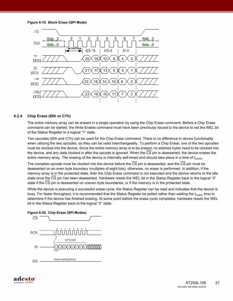
6.2.4 Chip Erase (60h or C7h)
The entire memory array can be erased in a single operation by using the Chip Erase command. Before a Chip Erase command can be started, the Write Enable command must have been previously issued to the device to set the WEL bit of the Status Register to a logical “1” state.
Two opcodes (60h and C7h) can be used for the Chip Erase command. There is no difference in device functionality when utilizing the two opcodes, so they can be used interchangeably. To perform a Chip Erase, one of the two opcodes must be clocked into the device. Since the entire memory array is to be erased, no address bytes need to be clocked into the device, and any data clocked in after the opcode is ignored. When the CS pin is deasserted, the device erases the entire memory array. The erasing of the device is internally self-timed and should take place in a time of tCHPE.
The complete opcode must be clocked into the device before the CS pin is deasserted, and the CS pin must be deasserted on an even byte boundary (multiples of eight bits); otherwise, no erase is performed. In addition, if the memory array is in the protected state, then the Chip Erase command is not executed and the device returns to the idle state once the CS pin has been deasserted. Hardware resets the WEL bit in the Status Register back to the logical “0” state if the CS pin is deasserted on uneven byte boundaries, or if the memory is in the protected state.
While the device is executing a successful erase cycle, the Status Register can be read and indicates that the device is busy. For faster throughput, it is recommended that the Status Register be polled rather than waiting the tCHPE time to determine if the device has finished erasing. At some point before the erase cycle completes, hardware resets the WEL bit in the Status Register back to the logical “0” state.
Figure 6-20. Chip Erase (SPI Modes)
SCK
CS
SI
SO
MSB
2 310
C C C C C C C C
6 754
OPCODE
HIGH-IMPEDANCE

28AT25SL128 DS-25SL128–090A–4/2016
Figure 6-21. Chip Erase (QPI Mode)
6.2.5 Program/Erase Suspend (75h)
In some code plus data storage applications, it is often necessary to process certain high-level system interrupts that require relatively immediate reading of code or data from the Flash memory. In such an instance, it may not be possible for the system to wait the microseconds or milliseconds required for the Flash memory to complete a program or erase cycle. The Program/Erase Suspend command allows a program or erase operation in progress to be suspended so that other device operations can be performed. For example, by suspending an erase operation to a particular block, the system can perform functions such as a program or read to a different block.
Chip Erase cannot be suspended. Hardware ignores the Program/Erase Suspend command if it is issued during a Chip Erase. A program operation can be performed while an erase operation is suspended, but the program operation cannot be suspended while an erase operation is currently suspended. Other device operations, such as a Read Status Register, can also be performed while a program or erase operation is suspended.
Since the need to suspend a program or erase operation is immediate, the Write Enable command does not need to be issued prior to the Program/Erase Suspend command being issued. Therefore, the Program/Erase Suspend command operates independently of the state of the WEL bit in the Status Register.
To perform a Program/Erase Suspend, the CS pin must first be asserted and the opcode of 75h must be clocked into the device. No address bytes need be clocked into the device, and any data clocked in after the opcode is ignored. When the CS pin is deasserted, the program or erase operation currently in progress suspends within a time of tSUSE. Hardware sets the Suspend (SUS) bit in the Status Register to indicate that the program or erase operation has been suspended. In addition, the RDY/BSY bit in the Status Register indicates that the device is ready for another operation. The complete opcode must be clocked into the device before the CS pin is deasserted, and the CS pin must be deasserted on a byte boundary (multiples of eight bits). Otherwise, no suspend operation is performed.
If a read operation is attempted to a suspended area (page for programming or block for erasing), then the device outputs undefined data. Therefore, when performing a Read Array operation to an unsuspended area and the device's internal address counter increments and crosses into the suspended area, the device starts outputting undefined data until the internal address counter crosses to an unsuspended area.
A program operation is not allowed to a block that has been erase suspended. If a program operation is attempted to an erase suspended block, then the program operation aborts and hardware clears the WEL bit in the Status Register. Likewise, an erase operation is not allowed to a block that included the page that has been program suspended. If attempted, the erase operation aborts and hardware resets the WEL bit in the Status Register.
If an attempt is made to perform an operation that is not allowed during a program or erase suspend, such as a Write Status Register operation, then the device simply ignores the opcode and no operation is performed. The state of the WEL bit in the Status Register is not affected.

29AT25SL128 DS-25SL128–090A–4/2016
Figure 6-22. Program/Erase Suspend (SPI Mode)
Figure 6-23. Program/Erase Suspend (QPI Mode)
Table 6-3. Operations Allowed and Not Allowed During a Program/Erase Suspend Command
Command During Program Suspend During Erase Suspend
Read CommandsRead Array (03h, 0Bh, 3Bh, BBh, 6Bh, EBh) Allowed Allowed
Continuous Read Reset (FFh) Allowed Allowed
Program and Erase CommandsBlock Erase (20h, 52h, D8h) Not Allowed Not Allowed
Chip Erase (C7h, 60h) Not Allowed Not Allowed
Byte/Page Program (02h) Not Allowed Allowed
Program/Erase Suspend (75h) Not Allowed Not Allowed
Program/Erase Resume (7Ah) Allowed Allowed
Protection CommandsWrite Enable (06h) Allowed Allowed
Write Disable (04h) Allowed Allowed
Security CommandsErase Security Register Page (44h) Not Allowed Not Allowed
Program Security Register Page (42h) Not Allowed Not Allowed
SCK
CS
SI
SO
MSB
2 310
0 1 1 1 0 1 0 1
6 754
OPCODE
HIGH-IMPEDANCE

30AT25SL128 DS-25SL128–090A–4/2016
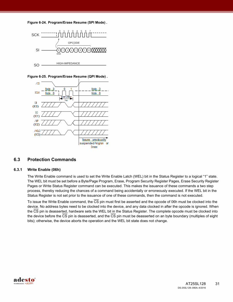
6.2.6 Program/Erase Resume (7Ah)
The Program/Erase Resume command allows a suspended program or erase operation to be resumed and continue programming a Flash page or erasing a Flash memory block where it left off. Hardware accepts the Program/Erase Resume command only if the SUS bit in the Status Register is set and the RDY/BSY bit is cleared. If the SUS bit equals 0 or the RDY/BSY bit equals to 1, the Program/Erase Resume command is ignored by the device. As with the Program/Erase Suspend command, the Write Enable command does not need to be issued prior to the Program/Erase Resume command being issued. Therefore, the Program/Erase Resume command operates independently of the state of the WEL bit in the Status Register.
To perform Program/Erase Resume, the CS pin must first be asserted and opcode 7Ah must be clocked into the device.
No address bytes need to be clocked into the device, and any data clocked in after the opcode is ignored. When the CS pin is deasserted, the program or erase operation currently suspended resumes within a time of tRES. Hardware then clears the SUS bit in the Status Register to indicate the program or erase operation is no longer suspended. In addition, the RDY/BSY bit in the Status Register indicates that the device is busy performing a program or erase operation. The complete opcode must be clocked into the device before the CS pin is deasserted, and the CS pin must be deasserted on a byte boundary (multiples of eight bits). Otherwise, no resume operation is performed.
During a simultaneous Erase Suspend/Program Suspend condition, issuing the Program/Erase Resume command results in the program operation resuming first. After the program operation has been completed, the Program/Erase Resume command must be issued again in order for the erase operation to be resumed.
While the device is busy resuming a program or erase operation, any attempts at issuing the Program/Erase Suspend command are ignored. Therefore, if a resumed program or erase operation needs to be subsequently suspended again, the system must either wait the entire tRES time before issuing the Program/Erase Suspend command, or it must check the status of the RDY/BSY bit or the SUS bit in the Status Register to determine if the previously suspended program or erase operation has resumed.
Read Security Register Page (48h) Allowed Allowed
Status Register CommandsRead Status Register (05h, 35h, 15h) Allowed Allowed
Write Status Register (01h, 31h, 11h) Not Allowed Not Allowed
Volatile Write Enable Status Register (50h) Not Allowed Not Allowed
Miscellaneous CommandsRead Manufacturer and Device ID (9Fh) Allowed Allowed
Read ID (90h) Allowed Allowed
Deep Power-Down (B9h) Not Allowed Not Allowed
Resume from Deep Power-Down (ABh) Allowed (1) Allowed
1. Allowed for reading Device ID.
Table 6-3. Operations Allowed and Not Allowed During a Program/Erase Suspend Command (Continued)
Command During Program Suspend During Erase Suspend
31AT25SL128 DS-25SL128–090A–4/2016
Figure 6-24. Program/Erase Resume (SPI Mode) .
Figure 6-25. Program/Erase Resume (QPI Mode) .
6.3 Protection Commands
6.3.1 Write Enable (06h)
The Write Enable command is used to set the Write Enable Latch (WEL) bit in the Status Register to a logical “1” state. The WEL bit must be set before a Byte/Page Program, Erase, Program Security Register Pages, Erase Security Register Pages or Write Status Register command can be executed. This makes the issuance of these commands a two step process, thereby reducing the chances of a command being accidentally or erroneously executed. If the WEL bit in the Status Register is not set prior to the issuance of one of these commands, then the command is not executed.
To issue the Write Enable command, the CS pin must first be asserted and the opcode of 06h must be clocked into the device. No address bytes need to be clocked into the device, and any data clocked in after the opcode is ignored. When the CS pin is deasserted, hardware sets the WEL bit in the Status Register. The complete opcode must be clocked into the device before the CS pin is deasserted, and the CS pin must be deasserted on an byte boundary (multiples of eight bits); otherwise, the device aborts the operation and the WEL bit state does not change.
SCK
SI
SO
MSB
2 310
0 1 1 1 1 0 1 0
6 754
OPCODE
HIGH-IMPEDANCE

32AT25SL128 DS-25SL128–090A–4/2016
Figure 6-26. Write Enable (SPI Mode)
Figure 6-27. Write Enable (QPI Mode)
6.3.2 Write Disable (04h)
The Write Disable command is used to reset the Write Enable Latch (WEL) bit in the Status Register to the logical “0” state. With the WEL bit reset, all Byte/Page Program, Erase, Program Security Register Page, and Write Status Register commands cannot be executed. Other conditions can also cause the WEL bit to be reset; for more details, refer to the WEL bit section of the Status Register description.
To issue the Write Disable command, the CS pin must first be asserted and the opcode of 04h must be clocked into the device. No address bytes need to be clocked into the device, and any data clocked in after the opcode is ignored. When the CS pin is deasserted, hardware clears the WEL bit in the Status Register. The complete opcode must be clocked into the device before the CS pin is deasserted, and the CS pin must be deasserted on an byte boundary (multiples of eight bits); otherwise, the device aborts the operation and the WEL bit state does not change.
Figure 6-28. Write Disable (SPI Mode)
SCK
CS
SI
SO
MSB
2 310
0 0 0 0 0 1 1 0
6 754
OPCODE
HIGH-IMPEDANCE
SCK
CS
SI
SO
MSB
2 310
0 0 0 0 0 1 0 0
6 754
OPCODE
HIGH-IMPEDANCE

33AT25SL128 DS-25SL128–090A–4/2016
Figure 6-29. Write Disable (QPI Mode)
6.3.3 Non-Volatile Protection
The device can be software protected against erroneous or malicious program or erase operations by utilizing the Non-Volatile Protection feature of the device. Non-Volatile Protection can be enabled or disabled by using the Write Status Register command to change the value of the Protection (CMP, SEC, TB, BP2, BP1, BP0) bits in the Status Register (refer to” Status Registers” in Section 7 for more information). The following table outlines the states of the Protection bits and the associated protection area.
.Table 6-4. Status Register Memory Array Protection — WPS = 0, CMP = 0
Protection Bits Memory Content
SEC TB BP2 BP1 BP0 Protected Address RangeProtected Memory
Size Portion
X X 0 0 0 None None None
0 0 0 0 1 FC0000h - FFFFFFh 256 KB Upper 1/64
0 0 0 1 0 F80000h - FFFFFFh 512 KB Upper 1/32
0 0 0 1 1 F00000h - FFFFFFh 1 MB Upper 1/16
0 0 1 0 0 E00000h - FFFFFFh 2 MB Upper 1/8
0 0 1 0 1 C00000h - FFFFFFh 4 MB Upper 1/4
0 0 1 1 0 800000h - FFFFFFh 8 MB Upper 1/2
0 1 0 0 1 000000h - 03FFFFh 256 KB Lower 1/64
0 1 0 1 0 000000h - 07FFFFh 512 KB Lower 1/32
0 1 0 1 1 000000h - 0FFFFFh 1 MB Lower 1/16
0 1 1 0 0 000000h - 1FFFFFh 2 MB Lower 1/8
0 1 1 0 1 000000h - 3FFFFFh 4 MB Lower 1/4
0 1 1 1 0 000000h - 7FFFFFh 8 MB Lower 1/2
X X 1 1 1 000000h - FFFFFFh 16 MB ALL
1 0 0 0 1 FFF000h - FFFFFFh 4 KB Upper 1/4096
1 0 0 1 0 FFE000h - FFFFFFh 8 KB Upper 1/2048
1 0 0 1 1 FFC000h - FFFFFFh 16 KB Upper 1/1024

34AT25SL128 DS-25SL128–090A–4/2016
1 0 1 0 X FF8000h - FFFFFFh 32 KB Upper 1/512
1 1 0 0 1 000000h - 000FFFh 4 KB Lower 1/4096
1 1 0 1 0 000000h - 001FFFh 8 KB Lower 1/2048
1 1 0 1 1 000000h - 003FFFh 16 KB Lower 1/1024
1 1 1 0 X 000000h - 007FFFh 32 KB Lower 1/512
Table 6-5. Status Register Memory Array Protection — WPS = 0, CMP = 1
Protection Bits Memory Content
SEC TB BP2 BP1 BP0 Address RangeProtected Memory
Size Portion
X X 0 0 0 000000h - FFFFFFh 16 MB All
0 0 0 0 1 000000h - FBFFFFh 16,128 KB Lower 63/64
0 0 0 1 0 000000h - F7FFFFh 15,872 KB Lower 31/32
0 0 0 1 1 000000h - EFFFFFh 15 MB Lower 15/16
0 0 1 0 0 000000h - DFFFFFh 14 MB Lower 7/8
0 0 1 0 1 000000h - BFFFFFh 12 MB Lower 3/4
0 0 1 1 0 000000h - 7FFFFFh 8 MB Lower 1/2
0 1 0 0 1 040000h - FFFFFFh 16,128 KB Upper 63/64
0 1 0 1 0 080000h - FFFFFFh 15,872 KB Upper 31/32
0 1 0 1 1 100000h - FFFFFFh 15 MB Upper 15/16
0 1 1 0 0 200000h - FFFFFFh 14 MB Upper 7/8
0 1 1 0 1 400000h - FFFFFFh 12 MB Upper 3/4
0 1 1 1 0 800000h - FFFFFFh 8 MB Upper 1/2
X X 1 1 1 NONE NONE NONE
1 0 0 0 1 000000h - FFEFFFh 16,380 KB Lower 4095/4096
1 0 0 1 0 000000h - FFDFFFh 16,376 KB Lower 2047/2048
1 0 0 1 1 000000h - FFBFFFh 16,368 KB Lower 1023/1024
1 0 1 0 X 000000h - FF7FFFh 16,352 KB Lower 511/512
1 1 0 0 1 001000h - FFFFFFh 16,380 KB Upper 4095/4096
Table 6-4. Status Register Memory Array Protection — WPS = 0, CMP = 0 (Continued)
Protection Bits Memory Content
SEC TB BP2 BP1 BP0 Protected Address RangeProtected Memory
Size Portion

35AT25SL128 DS-25SL128–090A–4/2016
As a safeguard against accidental or erroneous protecting or unprotecting of the memory array, the Protection can be locked from updates by using the WP pin (see “Protected States and the Write Protect Pin” on page 35 for more details).
6.3.4 Protected States and the Write Protect Pin
The WP pin is not linked to the memory array itself and has no direct effect on the protection status of the memory array. Instead, the WP pin, is used to control the hardware locking mechanism of the device.
If the WP pin is permanently connected to GND, then the protection bits cannot be changed.
6.4 Security Register Commands
The device contains three extra pages called Security Registers that can be used for purposes such as unique device serialization, system-level Electronic Serial Number (ESN) storage, locked key storage, etc. The Security Registers are independent of the main Flash memory.
Each page of the Security Register can be erased and programmed independently. Each page can also be independently locked to prevent further changes.
6.4.1 Erase Security Registers (44h)
The AT25SL128 offers three 256-byte Security Registers that can be independently erased and programmed. Before an erase Security Register Page command can be started, the Write Enable command must have been previously issued to the device to set the WEL bit of the Status Register to a logical "1" state.
To perform an Erase Security Register Page command, the CS pin must first be asserted and the opcode 44h must be clocked into the device. After the opcode has been clocked in, the three address bytes specifying the Security Register Page to be erased must be clocked in. The state of address bits 15:8 determine which register is accessed as described in Table 6-6 below. When the CS pin is deasserted, the device erases the appropriate block. The erasing of the block is internally self-timed and should take place in a time of tBE.
Since the Erase Security Register Page command erases a region of bytes, the lower order address bits do not need to be decoded by the device. Therefore address bits A7-A0 are ignored by the device. Despite the lower order address bits not being decoded by the device, the complete three address bytes must still be clocked into the device before the CS pin is deasserted, and the CS pin must be deasserted right after the last address bit (A0); otherwise, the device aborts the operation and no erase operation is performed.
While the device is executing a successful erase cycle, the Status Register can be read and indicates that the device is busy. For faster throughput, it is recommended that the Status Register be polled rather than waiting the tBE time to determine if the device has finished erasing. At some point before the erase cycle completes, hardware clears the RDY/BSY bit in the Status Register.
Hardware clears the WEL bit in the Status Register if the erase cycle aborts due to an incomplete address being sent, the CS pin being deasserted on uneven byte boundaries, or because a memory location within the region to be erased is protected.
1 1 0 1 0 002000h - FFFFFFh 16,376 KB Upper 2047/2048
1 1 0 1 1 004000h - FFFFFFh 16,368 KB Upper 1023/1024
1 1 1 0 X 008000h - FFFFFFh 16,352 KB Upper 511/512
Table 6-5. Status Register Memory Array Protection — WPS = 0, CMP = 1 (Continued)
Protection Bits Memory Content
SEC TB BP2 BP1 BP0 Address RangeProtected Memory
Size Portion

36AT25SL128 DS-25SL128–090A–4/2016
The Security Registers Lock bits (LB3-LB1) in the Status Register can be used to OTP protect the security registers. Once software sets the Lock bit is set, the corresponding Security Register becomes permanently locked. In this case, hardware ignores the Erase Security Register Page command for those Security Registers that have their Lock Bit set.
Figure 6-30. Erase Security Register Page
6.4.2 Program Security Registers (42h)
The Program Security Register command is similar to the Page Program command. It allows from one byte to 256 bytes of security register data to be programmed at previously erased (FFh) memory locations. The Program Security Registers command utilizes the internal 256-byte buffer for processing. Therefore, the contents of the buffer are altered from its previous state when this command is issued.
The Security Registers can be programmed in a similar fashion to the Program Array operation up to the maximum clock frequency specified by fCLK. Before a Program Security Registers command can be started, the Write Enable command must have been previously issued to the device (see “Write Enable (06h)” on page 31) to set the Write Enable Latch (WEL) bit of the Status Register to a logical “1” state. To program the Security Registers, the CS pin must first be asserted and the opcode of 42h must be clocked into the device. After the opcode has been clocked in, the three address bytes must be clocked in to specify the starting address location of the first byte to program within the Security Register. Bits 15:8 of the address indicate the Security register to be accessed as shown in Table 6-7 below.
Table 6-6. Security Register Addresses for Erase Security Register Page Command (SPI Mode Only)
Address A23-A16 A15-A8 A7-A0
Security Register 1 00H 01H Don’t Care
Security Register 2 00H 02H Don’t Care
Security Register 3 00H 03H Don’t Care
MSB
2 310 6 754
OPCODE
Table 6-7. Security Register Addresses for Program Security Registers Command
Address A23-A16 A15-A8 A7-A0
Security Register 1 00H 01H Byte Address
Security Register 2 00H 02H Byte Address
Security Register 3 00H 03H Byte Address

37AT25SL128 DS-25SL128–090A–4/2016
Figure 6-31. Program Security Registers (SPI Mode Only)
6.4.3 Read Security Registers (48h)
The Security Register can be sequentially read in a similar fashion to the Read Array operation up to the maximum clock frequency specified by fCLK. To read the Security Register, the CS pin must first be asserted and the opcode of 48h must be clocked into the device. After the opcode has been clocked in, the three address bytes must be clocked in to specify the starting address location of the first byte to read within the Security Register. Following the three address bytes, one dummy byte must be clocked into the device before data can be output. Bits 15:8 of the address indicate the Security register to be accessed as shown in Table 6-8 below.
After the three address bytes and the dummy byte have been clocked in, additional clock cycles result in Security Register data being output on the SO pin. When the last byte (0003FFh) of the Security Register has been read, the device continues reading back at the beginning of the register (000000h). No delays are incurred when wrapping around from the end of the register to the beginning of the register.
Deasserting the CS pin terminates the read operation and put the SO pin into a high - impedance state. The CS pin can be deasserted at any time and does not require that a full byte of data be read.
Figure 6-32. Read Security Registers (SPI Mode Only)
MSB MSB
2 310
0 0 1
6 754 98 3937 3833 36353431 3229 30
OPCODE
HIGH-IMPEDANCE
A A A A AAMSB
D D D D D D D D
ADDRESS BITS A23-A0 DATA IN BYTE 1
MSB
D D D D D D D D
DATA IN BYTE n
Table 6-8. Security Register Addresses for Read Security Registers Command
Address A23-A16 A15-A8 A7-A0
Security Register 1 00H 01H Byte Address
Security Register 2 00H 02H Byte Address
Security Register 3 00H 03H Byte Address
MSB MSB
2 310
0 1
6 754 10 1198 12 33 36353431 3229 30
OPCODE
A A A A A A AA A X X X
MSB MSB
D D D D D D D DDD
ADDRESS BITS A23-A0
MSB
X X X X X X
DATA BYTE 1
HIGH-IMPEDANCE

38AT25SL128 DS-25SL128–090A–4/2016
6.5 Status Register Commands
6.5.1 Read Status Register (05h, 35h, and 15h)
The Status Register can be read to determine the device's ready/busy status, as well as the status of many other functions such as Block Protection. The Status Register can be read at any time, including during an internally self-timed program or erase operation.
To read Status Register Byte 1, the CS pin must first be asserted and the opcode of 05h must be clocked into the device. To read Status Register Byte 2, the CS pin must first be asserted and the opcode of 35h must be clocked into the device. To read Status Register Byte 3, the CS pin must first be asserted and the opcode of 15h must be clocked into the device.
After the appropriate opcode has been clocked in, the device begins outputting the corresponding byte of data on the SO pin during every subsequent clock cycle. After the last bit (bit 0) of associated status register byte has been clocked out, the sequence repeats itself starting again with bit 7 as long as the CS pin remains asserted and the clock pin is being pulsed. The data in the Status Register is constantly being updated, so each repeating sequence may output new data. Deasserting the CS pin terminates the Read Status Register operation and put the SO pin into a high-impedance state. The CS pin can be deasserted at any time and does not require that a full byte of data be read.
Figure 6-33. Read Status Register Byte 1-3 (Command 05h/35h/15h)
Figure 6-34. Read Status Register Byte 1-3 (QPI Mode, Command 05h/35h/15h)
6.5.2 Write Status Register (01h/31h/11h)
The Write Status Register command is used to modify the Block Protection, Security Register Lock-down, Quad Enable, and Status Register Protection. Before the Write Status Register command can be issued, the Write Enable command must have been previously issued to set the WEL bit in the Status Register to a logical “1”.
SCK
CS
SI
SO
MSB
2 310
0 0 0 0 0 1 0 1
6 754 10 1198 12 21 2217 20191815 1613 14 23 24 28 29272625 30
MSB MSB
D D D D D D D DDDMSB
D D D D D DDD D D DD D D
BYTE 1
HIGH-IMPEDANCE
BYTE 1 BYTE 1
page 30 7.1.4b

39AT25SL128 DS-25SL128–090A–4/2016
To issue the Write Status Register command, the CS pin must first be asserted and the opcode of 01h must be clocked into the device followed by one or two bytes of data. The first byte of data consists of the SRP0, SEC, TB, BP2, BP1, BP0 bit values and 2 dummy bits. The second byte is optional and consists of 1 dummy bit, the CMP, LB3, LB2, LB1, 1 dummy bit, the QE, and 1 dummy bit. When the CS pin is deasserted, the bit values in the Status Register are modified, and hardware clears the WEL bit in the Status Register.
The complete one byte or two bytes of data must be clocked into the device before the CS pin is deasserted, and the CS pin must be deasserted on even byte boundaries (multiples of eight bits); otherwise, the device aborts the operation, the state of the Status Register bits do not change, memory protection status does not change, and the WEL bit in the Status Register are reset back to the logical “0” state.
Figure 6-35. Write Status Register (SPI Mode)
Table 6-9. Write Status Register 1 Format (Command 01h)
Bit 7 Bit 6 Bit 5 Bit 4 Bit 3 Bit 2 Bit 1 Bit 0
SRPO SEC TB BP2 BP1 BP0 WEL RDY/BSY
Table 6-10. Write Status Register 2 (Command 31h)
Bit 7 Bit 6 Bit 5 Bit 4 Bit 3 Bit 2 Bit 1 Bit 0
SUS CMP LB3 LB2 LB1 reserved QE SRP1
Table 6-11. Write Status Register 3 (Command 11h)
Bit 7 Bit 6 Bit 5 Bit 4 Bit 3 Bit 2 Bit 1 Bit 0
HOLD/RESET DRV1 DRV0 R R WPS R R
SI
SCK
SO
CS
MSB
2 310
0 0 0 0 0 0 0 1
6 754 10 1198 1917 1816
Opcode
D D D D
Status Register In - Byte 1
MSB
2321 222014 151312
D D D D D D D D
Status Register In - Byte 2
D D D D
High-Impedance
ALL C’s

40AT25SL128 DS-25SL128–090A–4/2016
Figure 6-36. Write Status Register (QPI Mode)
6.5.3 Write Enable for Volatile Status Register (50h)
During power up reset, the non-volatile Status Register bits are copied to a volatile version of the Status Register that is used during device operation. This gives more flexibility to change the system configuration and memory protection schemes quickly without waiting for the typical non-volatile bit write cycles or affecting the endurance of the Status Register non-volatile bits.
To write the volatile version of the Status Register bits, the Write Enable for Volatile Status Register (50h) command must be issued prior to each Write Status Register (01h) command. The Write Enable for Volatile Status Register command does not set the Write Enable Latch (WEL) bit. It is only valid for the next following Write Status Register command, to change the volatile Status Register bit values.
This command is available in both SPI and QPI modes.
Figure 6-37. Write Enable for Volatile Status Register
Figure 6-38. Write Enable for Volatile Status Register (QPI Mode)
MSB
2 310 6 754
OPCODE
HIGH-IMPEDANCE

41AT25SL128 DS-25SL128–090A–4/2016
6.6 Power Down Commands
6.6.1 Deep Power-Down (B9h)
During normal operation, hardware places the device in the standby mode to consume less power as long as the CS pin remains deasserted and no internal operation is in progress. The Deep Power-Down command offers the ability to place the device into an even lower power consumption state called the Deep Power-Down mode.
When the device is in the Deep Power-Down mode, hardware ignores all commands with the exception of the Resume from Deep Power-Down command. Since all commands are ignored in this mode, the mode can be used as an extra protection mechanism against program and erase operations.
Entering the Deep Power-Down mode is accomplished by simply asserting the CS pin, clocking in the opcode of B9h, and then deasserting the CS pin. Any additional data clocked into the device after the opcode is ignored. When the CS pin is deasserted, the device enters the Deep Power-Down mode within the maximum time of tEDPD.
The complete opcode must be clocked in before the CS pin is deasserted, and the CS pin must be deasserted on an byte boundary (multiples of eight bits); otherwise, the device aborts the operation and return to the standby mode once the CS pin is deasserted. In addition, the device defaults to the standby mode after a power-cycle.
Hardware ignores the Deep Power-Down command if an internally self-timed operation such as a program or erase cycle is in progress. The Deep Power-Down command must be reissued after the internally self-timed operation has been completed in order for the device to enter the Deep Power-Down mode.
This command is available in both SPI and QPI modes.
Figure 6-39. Deep Power-Down (SPI Mode)
SCK
CS
SI
SO
MSB
ICC
2 310
1 0 1 1 1 0 0 1
6 754
OPCODE
HIGH-IMPEDANCE
Standby Mode Current
Active Current
Deep Power-Down Mode Current
tEDPD

42AT25SL128 DS-25SL128–090A–4/2016
Figure 6-40. Deep Power-Down (QPI Mode)
6.6.2 Resume from Deep Power-Down (ABh)
In order to exit the Deep Power-Down mode and resume normal device operation, the Resume from Deep Power-Down command must be issued. The Resume from Deep Power-Down command is the only command that the device recognizes while in the Deep Power-Down mode.
To resume from the Deep Power-Down mode, the CS pin must first be asserted and the opcode of ABh must be clocked into the device. Any additional data clocked into the device after the opcode is ignored. When the CS pin is deasserted, the device exits the Deep Power-Down mode within the maximum time of tRDPD and return to the standby mode. After the device has returned to the standby mode, normal command operations such as Read Array can be resumed.
If the complete opcode is not clocked in before the CS pin is deasserted, or if the CS pin is not deasserted on an byte boundary (multiples of eight bits), then the device aborts the operation and return to the Deep Power-Down mode.
This command is available in both SPI and QPI modes.
Figure 6-41. Resume from Deep Power-Down (SPI Mode)
MSB
2 310
1 0 1 0 1 0 1 1
6 754
OPCODE
HIGH-IMPEDANCE
Deep Power-Down Mode Current
Active Current
Standby Mode Current
tRDPD

43AT25SL128 DS-25SL128–090A–4/2016
Figure 6-42. Resume from Deep Power-Down (QPI Mode)
6.6.3 Resume from Deep Power-Down and Read Device ID (ABh)
The Resume from Deep Power-Down command can also be used to read the Device ID.
When used to release the device from the Power-Down state and obtain the Device ID, the CS pin must first be asserted and opcode of ABh must be clocked into the device, followed by 3 dummy bytes. The Device ID bits are then shifted out on the falling edge of SCLK with most significant bit (MSB) first as shown in Figure 6-43. This command only outputs a single byte Device ID. The Device ID value for the AT25SL128 is listed in Table 8-2.
After the last bit (bit 0) of the Device ID has been clocked out, the sequence repeats itself starting again with bit 7 as long as the CS pin remains asserted and the SCK pin is being pulsed. After CS is deasserted it must remain high for a time duration of tRDPO before new commands can be received.
The same command may be used to read device ID when not in power down. In that case, CS does not have to remain high after it is deasserted.
This command is available in both SPI and QPI modes.
Figure 6-43. Resume from Deep Power-Down and Read Device ID (SPI Mode)
MSB
2 310
1 0 1 0 1 0 1 1
6 754
OPCODE
HIGH-IMPEDANCE
Active Current
31 323029 38 393735 363433
X X X X X
MSB
D D D D D D D D

44AT25SL128 DS-25SL128–090A–4/2016
Figure 6-44. Resume from Deep Power-Down and Read Device ID (QPI Mode)
6.7 Lock and Unlock Commands
6.7.1 Individual Block Lock (36h)
The Individual Block Lock command can be used to protect the memory array from being erased via the Erase commands. To enable the block lock function, the WPS bit in Status Register 3 must be set. If WPS is cleared, write protection is then determined by the combination of the CMP, SEC, TB, and BP[2:0] bits in the Status Registers. The default value for each of these bits is 1 at power-up or reset, so the entire memory array is being protected.
An Individual Block Lock command is executed by first driving the CS pin low, then shifting opcode 36h onto the bus, followed by a 24-bit address. A Write Enable command must be executed before the device accepts the Individual Block Lock command (Status Register bit WEL= 1).
Figure 6-45. Individual Block Lock Command (SPI Mode)
Figure 6-46. Individual Block Lock Command (Quad I/O Mode)

45AT25SL128 DS-25SL128–090A–4/2016
6.7.2 Individual Block Unlock (39h)
The Individual Block Unlock command can be used to protect the memory array from being erased via the Erase commands. To enable the block lock function, the WPS bit in Status Register 3 must be set. If WPS is cleared, write protection is then determined by the combination of the CMP, SEC, TB, and BP[2:0] bits in the Status Registers. The default value for each of these bits is 1 at power-up or reset, so the entire memory array is being protected.
An Individual Block Unlock command is executed by first driving the CS pin low, then shifting opcode 39h onto the bus, followed by a 24-bit address. A Write Enable command must be executed before the device accepts the Individual Block Lock command (Status Register bit WEL= 1).
Figure 6-47. Individual Block Unlock Command (SPI Mode)
Figure 6-48. Individual Block Unlock Command (QPI Mode)
6.7.3 Read Block Lock (3Dh)
The Read Block Lock command can be used to protect the memory array from being erased via the Erase commands. To enable the read block lock function, the WPS bit in Status Register 3 must be set. If WPS is cleared, write protection is then determined by the combination of the CMP, SEC, TB, and BP[2:0] bits in the Status Registers. The default value for each of these bits is 1 at power-up or reset, so the entire memory array is being protected.
An Individual Block Unlock command is executed by first driving the CS pin low, then shifting opcode 3Dh onto the bus, followed by a 24-bit address. A Write Enable command must be executed before the device accepts the Individual Block Lock command (Status Register bit WEL= 1).
Once the command and address have been transmitted, the memory device shifts out the Read Block Lock bit values is onto the Data Output pin at the falling edge of SCK. The most significant bit (MSB) first is output first. If the least significant bit (LSB) is 1, the corresponding block is locked. If the LSB = 0, the corresponding block is unlocked, indicating that an Erase/Program operation can be performed on this location.

46AT25SL128 DS-25SL128–090A–4/2016
Figure 6-49. Read Block Lock Command (SPI Mode)
Figure 6-50. Read Block Lock Command (QPI Mode)
6.7.4 Global Block Lock (7Eh)
The Global Block Lock command can be used to lock all block lock bits simultaneously. The command is executed by driving the CS pin low and shifting opcode 7Eh into the device. Note that a Write Enable command must be executed before the device can accept the Global Block Lock command (Status Register bit WEL= 1).
This command is available in both SPI and QPI modes.
Figure 6-51. Global Block Lock Command for SPI Mode (left) or QPI Mode (right)

47AT25SL128 DS-25SL128–090A–4/2016
6.7.5 Global Block Unlock (98h)
The Global Block Unlock command can be used to unlock all block lock bits simultaneously. The command is executed by driving the CS pin low and shifting opcode 98h into the device. Note that a Write Enable command must be executed before the device can accept the Global Block Lock command (Status Register bit WEL= 1).
This command is available in both SPI and QPI modes.
Figure 6-52. Global Block Unlock Command for SPI Mode (left) or Quad I/O Mode (right)
6.8 Miscellaneous Commands
6.8.1 Enable Reset (66h) and Device Reset (99h)
Due the limited pin count on the AT25SL128 memory device, two Reset commands are used to reset the device as opposed to an actual reset pin. Executing the Reset command terminates all internal operations. After reset, the device is set to its default parameters and all previous register settings are lost.
To initiate a device reset, the Enable Reset command (66h) is issued first, followed by the Device Reset command (99h). If any other command is issued after the Enable Reset command, the Reset Enable command is disabled the subsequent command is executed. To perform a device reset, command 66h must be followed by command 99h. Both command can be issued in both SPI mode and QPI mode. During the reset sequence, no other command can be accepted by the device.
Note that is an erase or program operation has been suspended and the device reset sequence is initiated, the data will be corrupted. To prevent this from happening, check the BUSY and the SUS bits in Status Register before issuing the Reset command sequence.
Figure 6-53. Enable Reset and Reset Command Sequence (SPI Mode)

48AT25SL128 DS-25SL128–090A–4/2016
Figure 6-54. Enable Reset and Reset Command Sequence (QPI Mode)
6.8.2 Enter QPI Mode (38h)
In order to enter the QPI Mode from the Standard SPI Mode, an Enter QPI Mode command (38h) must be issued. The Enter QPI Mode command can only be entered from Standard SPI Mode. Before the Enter QPI Mode command can be issued, the Write Enable (06h) command must have been previously issued to set the WEL bit in the Status Register to a logical “1”.
To issue the Enter QPI Mode command, the CS pin must first be asserted and the opcode of 38h must be clocked into the device. When the device is switched from SPI Mode to QPI Mode, the existing Program Suspend status, Erase Suspend status, and the Wrap Length settings remain unchanged. The WEL bit in the Status Register is reset back to the logical “0” state.
Figure 6-55. Enter QPI Command (SPI Mode only)
6.8.3 Exit QPI Mode (FFh)
The Exit QPI Mode command is used to exit the QPI mode and return to the Standard/Dual/Quad SPI mode. When the device is switched from QPI mode to SPI mode, the existing Write Enable Latch (WEL), Erase Suspend status, and Wrap Length setting remains unchanged. This command is executed only in QPI mode.

49AT25SL128 DS-25SL128–090A–4/2016
Figure 6-56. Exit QPI Command (QPI Mode only)
6.8.4 Set Burst with Wrap (77h)
The Set Burst with Wrap (77h) command is used in conjunction with the Quad I/O Read (EBh) and Quad I/O Word Read (E7h) commands to access data with various wrap lengths.
The Set Burst with Wrap command is initiated by driving the CS pin low and then shifting opcode 77h into the device, followed by 24 dummy bits and 8 Wrap Bits (W[7:0]. Bits 6 and 5 of this field are used to determine the wrap length as shown in Table 6-12. The W4 bit is the enable bit for the wrap feature.
To exit the Wrap Around function and return to the normal read mode, another Set Burst with Wrap command should be issued to set W4 = 1. The default value of W4 upon power on or after a software/hardware reset is 1.
Table 6-12. Setting the Wrap Length
W6 W5
W4 = 0 W4 =1 (DEFAULT)
Wrap Around Wrap Length Wrap Around Wrap Length
0 0 Yes 8-byte No N/A
0 1 Yes 16-byte No N/A
1 0 Yes 32-byte No N/A
1 1 Yes 64-byte No N/A

50AT25SL128 DS-25SL128–090A–4/2016
Figure 6-57. Set Burst with Wrap Command (SPI Mode only)
6.8.5 Burst Read with Wrap (0Ch)
The Burst Read with Wrap (0Ch) command operates in QPI mode and implements a wrap-around feature. It differs from the Read Data Array command (0Bh) in that the read operation wrap around back to the beginning address once the ending address is reached. The ending address depends on the wrap length.
This command works in conjunction with the Set Read Parameters (C0h) command to set the wrap length and the number of dummy clocks. Refer to Section 6.8.6, Set Read Parameters (C0h) for more information.
Figure 6-58. Burst Read with Wrap Command (QPI Mode only)
6.8.6 Set Read Parameters (C0h)
The Set Read Parameters command (C0h) works in conjunction with the following command in QPI mode to set the wrap around length and the number of dummy clocks, which allows flexibility of the AT25SL128 device to accommodate a range of frequencies and data latencies.
• Read Data (0Bh)
• Quad I/O Read Data (EBh)
• Burst Read with Wrap (0Ch)

51AT25SL128 DS-25SL128–090A–4/2016
When this command is executed, an 8-bit opcode (C0h) is driven onto the bus, followed by an 8-bit parameters field (P[7:0]). This field contains the wrap length and the number of dummy clocks as shown in the following tables. Note that this command is not supported in standard SPI mode.
Figure 6-59. Set Read Parameters Command (QPI Mode only)
6.8.7 Read SFDP (5Ah)
The AT25SL128 contains a 256-byte Serial Flash Discoverable Parameter (SFDP) register.
The SFDP Register can be sequentially read in a similar fashion to the Read Array operation up to the maximum clock frequency specified by fCLK. To read the SFDP Security Register, the CS pin must first be asserted and the opcode of 5Ah must be clocked into the device. After the opcode has been clocked in, the three address bytes must be clocked in to specify the starting address location of the first byte to read within the SFDP Security Register. Following the three address bytes, an additional dummy byte needs to be clocked into the device. After the three address bytes and the dummy byte have been clocked in, additional clock cycles result in data being output on the I/O pin(s). The data is always output with the MSB of a byte first. When the last byte (0000FFh) of the SFDP Security Register has been read, the
Table 6-13. Encoding of P5:4 Field of the Set Read Parameters Command
P5 P4 Dummy clocks Maximum Read Frequency
0 0 2 33MHz
0 1 4 55MHz
1 0 6 80MHz
1 1 8 104MHz
Table 6-14. Encoding of P1:0 Field of the Set Read Parameters Command
P1 P0 Wrap Length
0 0 8 bytes
0 1 16 bytes
1 0 32 bytes
1 1 64 bytes
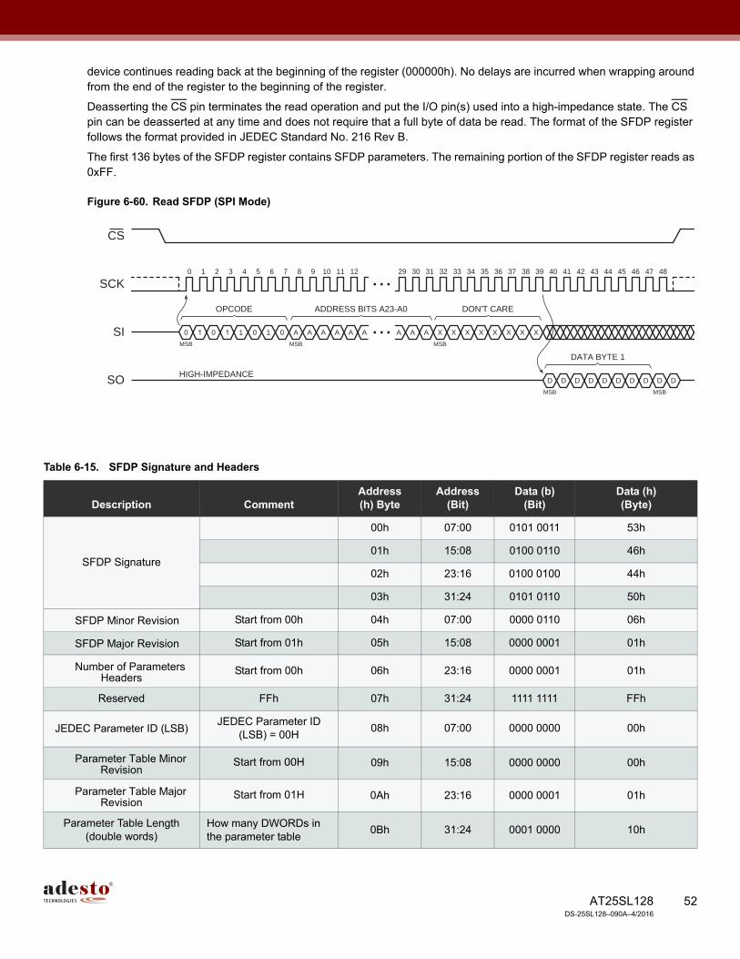
52AT25SL128 DS-25SL128–090A–4/2016
device continues reading back at the beginning of the register (000000h). No delays are incurred when wrapping around from the end of the register to the beginning of the register.
Deasserting the CS pin terminates the read operation and put the I/O pin(s) used into a high-impedance state. The CS pin can be deasserted at any time and does not require that a full byte of data be read. The format of the SFDP register follows the format provided in JEDEC Standard No. 216 Rev B.
The first 136 bytes of the SFDP register contains SFDP parameters. The remaining portion of the SFDP register reads as 0xFF.
Figure 6-60. Read SFDP (SPI Mode)
SCK
CS
SI
SO
MSB MSB
2 310
0 0 1 0 1
6 754 10 1198 12 39 42 43414037 3833 36353431 3229 30 44 47 484645
OPCODE
A A A A A A AA AMSB
X X X X X X X X
MSB MSB
D D D D D D D DDD
ADDRESS BITS A23-A0 DON'T CARE
DATA BYTE 1
HIGH-IMPEDANCE
Table 6-15. SFDP Signature and Headers
Description CommentAddress(h) Byte
Address (Bit)
Data (b)(Bit)
Data (h)(Byte)
SFDP Signature
00h 07:00 0101 0011 53h
01h 15:08 0100 0110 46h
02h 23:16 0100 0100 44h
03h 31:24 0101 0110 50h
SFDP Minor Revision Start from 00h 04h 07:00 0000 0110 06h
SFDP Major Revision Start from 01h 05h 15:08 0000 0001 01h
Number of ParametersHeaders
Start from 00h 06h 23:16 0000 0001 01h
Reserved FFh 07h 31:24 1111 1111 FFh
JEDEC Parameter ID (LSB)JEDEC Parameter ID
(LSB) = 00H08h 07:00 0000 0000 00h
Parameter Table MinorRevision
Start from 00H 09h 15:08 0000 0000 00h
Parameter Table MajorRevision
Start from 01H 0Ah 23:16 0000 0001 01h
Parameter Table Length (double words)
How many DWORDs in the parameter table
0Bh 31:24 0001 0000 10h

53AT25SL128 DS-25SL128–090A–4/2016
Table 6-16. SFDP Parameters Table 1
Parameter Table Pointer Address of Adesto Parameter Table
0Ch 07:00 0011 0000 30h
0Dh 15:08 0000 0000 00h
0Eh 23:16 0000 0000 00h
JEDEC Parameter ID (MSB)JEDEC Parameter ID
(MSB):FFH 0Fh 31:24 1111 1111 FFh
JEDEC Parameter ID (LSB) Adesto Manufacturer ID 10h 07:00 0001 1111 1Fh
Parameter Table MinorRevision
Start from 00H 11h 15:08 0000 0000 00h
Parameter Table MajorRevision
Start from 01H 12h 23:16 0000 0001 01h
Parameter Table Length (double words)
How many DWORDs in the parameter table
13h 31:24 0000 0010 02h
Parameter Table Pointer (PTP)
Address of Adesto Parameter Table
14h 07:00 1000 0000 80h
15h 15:08 0000 0000 00h
16h 23:16 0000 0000 00h
Reserved FFh 17h 31:24 1111 1111 FFh
Table 6-15. SFDP Signature and Headers
Description CommentAddress(h) Byte
Address (Bit)
Data (b)(Bit)
Data (h)(Byte)
Description CommentAddress(h) Byte
Address (Bit)
Data (b)(Bit)
Data (h)(Byte)
Erase Granularity01:4KB available
11:4KB not available
30h
01:00 01
E1h
Write Granularity 0:1Byte, 1:64 bytes or larger 02 0
Volatile Status Register Block Protect Bits
0: Nonvolatile status bit
1: Volatile status bit 03 0
Volatile Status Register Write Enable Opcode
0:50H Opcode to enable, if bit-3 = 1
04 0
Reserved 07:05 111
4KB Erase Opccde Opcode or FFh 31h 15:08 0010 0000 20h

54AT25SL128 DS-25SL128–090A–4/2016
Fast Dual Read Output(1 -1 -2)
0=Not supported, 1=Supported
32h
16 1
F1h
Number of Address Bytes 00:3 Byte only
01:3 or 4 Byte
10:4 Byte only
11:Reserved
18:17 00
Double Transfer Rate (DTR) Clocking
0=Not supported, 1=Supported 19 0
Fast Dual I/O Read (1-2- 2)
0=Not supported, 1=Supported 20 1
Fast Quad I/O Read (1-4-4)
0=Not supported, 1=Supported 21 1
Fast Quad Output Read (1-1-4)
0=Not supported, 1=Supported 22 1
Reserved FFh 23 1
Reserved FFh 33h 31:24 1111 1111 FFh
Flash Memory Density
34h 07:00 1111 1111 FFh
35h 15:08 1111 1111 FFh
36h 23:16 1111 1111 FFh
37h 31:24 0000 0111 07h
Fast Quad I/O (1-4-4) Number of dummy clocks
number of dummy clocks
38h
04:00 00100
44hFast Quad I/O (1-4-4) Number of mode bits
number of mode bits 07:05 010
Fast Quad I/O (1-4-4) Read Opcode
Opcode or FFh 39h 15:08 1110 1011 EBh
Fast Quad Output (1-1-4) Number of dummy clocks
number of dummy clocks
3Ah
20:16 01000
08hFast Quad Output (1-1-4) Number of mode bits
number of mode bits 23:21 000
Fast Quad Output (1-1-4) Read Opcode
Opcode or FFh 3Bh 31:24 0110 1011 6Bh
Fast Dual Output (1-1-2) Number of dummy clocks
number of dummy clocks
3Ch
04:00 01000
08hFast Dual Output (1-1-2) Number of mode bits
number of mode bits 07:05 000
Fast Dual Output (1-1-2) Read Opcode
Opcode or FFh 3Dh 15:08 0011 1011 3Bh
Description CommentAddress(h) Byte
Address (Bit)
Data (b)(Bit)
Data (h)(Byte)

55AT25SL128 DS-25SL128–090A–4/2016
Fast Dual I/O (1-2-2) Number of dummy clocks
number of dummy clocks
3Eh
20:16 00000
80hFast Dual I/O (1-2-2) Number of mode bits
number of mode bits 23:21 100
Fast Dual I/O (1-2-2) Read Opcode
Opcode or FFh 3Fh 31:24 1011 1011 BBh
Fast Dual DPI (2-2-2) 0=Not supported, 1=Supported
40h
0 0
FEhReserved FFh 03:01 111
Fast Quad QPI (4-4-4) 0=Not supported, 1=Supported 04 1
Reserved FFh 07:05 111
Reserved FFh 41h 15:08 1111 1111 FFh
Reserved FFh 42h 23:16 1111 1111 FFh
Reserved FFh 43h 31:24 1111 1111 FFh
Reserved FFh 44h 07:00 1111 1111 FFh
Reserved FFh 45h 15:08 1111 1111 FFh
Fast Dual DPI (2-2-2) Number of dummy clocks
number of dummy clocks
46h
20:16 0 0000
00hFast Dual DPI (2-2-2) Number of mode bits
number of mode bits 23:21 000
Fast Dual DPI(2-2-2) Read Opcode
Opcode or FFh 47h 31:24 1111 1111 FFh
Reserved FFh 48h 07:00 1111 1111 FFh
Reserved FFh 49h 15:08 1111 1111 FFh
Fast Quad QPI (4-4-4) Number of dummy clocks
number of dummy clocks
4Ah
20:16 00010
02hFast Quadl QPI (4-4-4) Number of mode bits
number of mode bits 23:21 000
Fast Quad QPI(4-4-4) Read Opcode
Opcode or FFh 4Bh 31:24 0000 1011 0Bh
Erase type-1 Size 4KB=2^0Ch, 32KB=2^0Fh,64KB=2^10h;
(2^Nbyte)
4Ch07:00
0000 1100 OCh
Erase type-1 Opcode Opcode or FFh 4Dh 15:08 0010 0000 20h
Erase type-2 Size 4KB=2^0Ch, 32KB=2^0Fh,64KB=2^10h;
(2^Nbyte)4Eh 23:16 0000 1111 0Fh
Erase type-2 Opcode Opcode or FFh 4Fh 31:24 0101 0010 52h
Description CommentAddress(h) Byte
Address (Bit)
Data (b)(Bit)
Data (h)(Byte)

56AT25SL128 DS-25SL128–090A–4/2016
Erase Type-3 Size 4KB=2^0Ch, 32KB=2^0Fh,64KB=2^10h;
(2^Nbyte)50h
07:000001 0000 10h
Erase Type-3 Opcode Opcode or FFh 51h 15:08 1101 1000 D8h
Erase Type-4 Size 4KB=2^0Ch, 32KB=2^0Fh,64KB=2^10h;
(2^Nbyte)52h 23:16 0000 0000 00h
Erase Type-4 Opcode Opcode or FFh 53h 31:24 1111 1111 FFh
Erase Maximum/Typical Ratio
Maximum = 2 * (COUNT + 1) * Typical
54h
55h
56h
57h
03:00 0010
32h
92h
0Dh
01h
Erase type-1 Typical time Count or 00h 08:04 0 0011
Erase type-1 Typical units
00b: 1ms
01b: 16ms
10b: 128ms
11b: 1s
10:09 01
Erase type-2 Typical time Count or 00h 15:11 1001 0
Erase type-2 Typical units
00b: 1ms
01b: 16ms
10b: 128ms
11b: 1s
17:16 01
Erase type-3 Typical time Count or 00h 22:18 000 11
Erase type-3 Typical units
00b: 1ms
01b: 16ms
10b: 128ms
11b: 1s
24:23 1 0
Erase type-4 Typical time Count or 00h 29:25 00 000
Erase type-4 Typical units
00b: 1ms
01b: 16ms
10b: 128ms
11b: 1s
31:30 00
Program Maximum/Typical Ratio
Maximum = 2 * (COUNT + 1) * Typical 58h
03:00 001082h
Page Size 2^N bytes 07:04 1000
Description CommentAddress(h) Byte
Address (Bit)
Data (b)(Bit)
Data (h)(Byte)

57AT25SL128 DS-25SL128–090A–4/2016
Program Page Typical time Count or 00h
59h
5Ah
5Bh
12:08 0 1010
EAh
14h
CEh
Program Page Typical units0: 8us,
1: 64us13 1
Program Byte Typical time, 1st byte
Count or 00h 17:14 00 11
Program Byte Typical units, 1st byte
0: 1us,
1: 8us18 1
Program Additional Byte Typical time
Count or 00h 22:19 0010
Program Additional Byte Typical units
0: 1us,
1: 8us23 0
Erase Chip Typical time Count or 00h 28:24 0 1110
Erase Chip Typical units
00b: 16ms
01b: 256ms
10b: 4s
11b: 64s
30:29 10
Reserved 1h 31 1
Prohibited Op during Program Suspend
see datasheet
5Ch
03:00 1101
EDhProhibited Op during Erase Suspend
see datasheet 07:04 1110
Description CommentAddress(h) Byte
Address (Bit)
Data (b)(Bit)
Data (h)(Byte)

58AT25SL128 DS-25SL128–090A–4/2016
Reserved1h
5Dh
5Eh
5Fh
08 1
61h
06h
33h
Program Resume to Suspend time
Count of 64us 12:09 0 000
Program Suspend Maximum time
Count or 00h 17:13 10 011
Program Suspend Maximum units
00b: 128ns,
01b: 1us,
10b: 8us,
11b: 64us
19:18 01
Erase Resume to Suspend time
Count of 64us 23:20 0000
Erase Suspend Maximum time
Count or 00h 28:24 1 0011
Erase Suspend Maximum units
00b: 128ns,
01b: 1us,
10b: 8us,
11b: 64us
30:29 01
Suspend / Resume supported
0: Program and Erase suspend supported
1: not supported
31 0
Program Resume Opcode Opcode or FFh 60h 7:0 0111 1010 7Ah
Program Suspend Opcode Opcode or FFh 61h 15:8 0111 0101 75h
Resume Opcode Opcode or FFh 62h 23:16 0111 1010 7Ah
Suspend Opcode Opcode or FFh 63h 31:24 0111 0101 75h
Reserved 11b
64h
01:00 11
F7hStatus Register Busy Polling
xxxxx1b: Opcode = 05h, bit-0 = 1 Busy,
xxxx1xb: Opcode = 70h, bit-7 = 0 Busy,
others: reserved
07:02 1111 01
Description CommentAddress(h) Byte
Address (Bit)
Data (b)(Bit)
Data (h)(Byte)

59AT25SL128 DS-25SL128–090A–4/2016
Exit Deep Powerdown time Count or 00h
65h
66h
67h
12:08 0 0010
A2h
D5h
5Ch
Exit Deep Powerdown units
00b: 128ns,
01b: 1us,
10b: 8us,
11b: 64us
14:13 01
Exit Deep Powerdown Opcode
Opcode or FFh 22:15 101 0101 1
Enter Deep Powerdown Opcode
Opcode or FFh 30:23 101 1100 1
Deep Powerdown Supported0: Deep Powerdown supported,
1: not supported
31 0
Disable 4-4-4 Read Mode
68h
69h
6Ah
03:00 1001
19h
B6h
49h
Enable 4-4-4 Read Mode 08:04 0 0001
Fast Quad I/O Continuous (0-4-4) supported
0: not supported,
1: Quad I/O 0-4-4 supported09 1
Fast Quad I/O Continuous (0-4-4) Exit
15:10 1011 01
Fast Quad I/O Continuous (0-4-4) Enter
19:16 1001
Quad Enable Requirements (QER)
22:20 100
HOLD or RESET Disable
0: not supported,
1: use Configuration Register bit-4
23 0
Reserved FFh 6Bh 31;24 1111 1111 FFh
Status Register Opcode6Ch
06:00 110 1000 E8h
Reserved 1h 07 1
Soft Reset Opcodes 6Dh 13:08 01 000010h, C0h
4-Byte Address Exit 6Eh 23:14 1100 0000 00
4-Byte Address Enter 6Fh 31:24 1000 0000 80h
Description CommentAddress(h) Byte
Address (Bit)
Data (b)(Bit)
Data (h)(Byte)

60AT25SL128 DS-25SL128–090A–4/2016
Table 6-17. SFDP Parameters Table 2
Description CommentAddress(h) Byte
Address (Bit)
Data (b)(Bit)
Data (h)(Byte)
VCC Minimum Voltage
1650h: 1.65V,
1700h: 1.70V,
2300h: 2.30V,
2500h: 2.50V,
2700h: 2.70V
80h
81h15:0
0101 0000
0001 011016h,50h
VCC Maximum Voltage
1950h: 1.95V,
3600h: 3.60V,
4000h: 4.00V,
4400h: 4.40V
82h
83h31:16
0101 0000
0001 100119h,50h
Array Protection Method10b: use non-volatile
status register
84h
85h
01:00 10
DAh
06h
Power up Protection default0: power up unprotected,
1: power up protected02 0
Protection Disable Opcodes 011b: use status register 05:03 01 1
Protection Enable Opcodes 011b: use status register 08:06 0 11
Protection Read Opcodes 011b: use status register 11:09 011
Protection Register Erase Opcode
00b: not supported,
01b: Opcodes 3Dh,2Ah,7Fh,CFh,
13:12 00
Protection Register Program Opcode
00b: not supported,
01b: Opcodes 3Dh,2Ah,7Fh,FCh
15:14 00
Reserved FFh 86h 23:16 1111 1111 FFh
Reserved FFh 87h 31:24 1111 1111 FFh
Reserved FFh 88h-FFh FFh

61AT25SL128 DS-25SL128–090A–4/2016
7. Status Registers
The AT25SL128 device contains three status registers as described in the following tables.
Table 7-1. Status Register Format - Byte 1
Table 7-2. Status Register Format – Byte 2
Bit (1)
1. Only bits 7 through 2 of the Status Register can be modified when using the Write Status Register command.
Name Type (2)
2. R/W = Read and Write; R = Read only
Description
7 SRP0 Status Register Protection bit-0 R/W See Table 7-4 on Status Register Protection
6 SEC Block Protection R/W See Table 6-4 and 6-5 on Non-Volatile Protection
5 TB Top or Bottom Protection R/W See Table 6-4 and 6-5 on Non-Volatile Protection
4 BP2 Block Protection bit-2 R/W See Table 6-4 and 6-5 on Non-Volatile Protection
3 BP1 Block Protection bit-1 R/W See Table 6-4 and 6-5 on Non-Volatile Protection
2 BP0 Block Protection bit-0 R/W See Table 6-4 and 6-5 on Non-Volatile Protection
1 WEL Write Enable Latch Status R0 Device is not Write Enabled (default)
1 Device is Write Enabled
0 RDY/BSY Ready/Busy Status R0 Device is ready
1 Device is busy with an internal operation
Bit (1)
1. Only bits 6 through 3, 1, and 0 of the Status Register can be modified when using the Write Status Register command
Name Type (2)
2. R/W = Read and Write; R = Read only
Description
7 SUS Suspend Status R0 Device is not suspended (default)
1 Device is suspended
6 CMP Complement Block Protection R/W 0 See table on Block Protection
5 LB3 Lock Security Register 3 R/W0 Security Register 3 is not locked (default)
1 Security Register 3 is locked
4 LB2 Lock Security Register 2 R/W0 Security Register 2 is not locked (default)
1 Security Register 2 is locked
3 LB1 Lock Security Register 1 R/W0 Security Register 1 is not locked (default)
1 Security Register 1 is locked
2 RES Reserved for future use R na Reserved for future use
1 QE Quad Enable R/W
0 0=Quad mode is not enabled
1=Quad mode is enabled
HOLD and WP are I/O pins1
0 SRP1 Status Register Protect bit-1 R/W See table on Status Register Protection

62AT25SL128 DS-25SL128–090A–4/2016
Table 7-3. Status Register Format – Byte 3
7.1 Status Register Protect Table
Notes: 1. When SRP1, SRP0 = (1, 0), a power-down, power-up cycle changes SRP1,SRP0 to the 0,0 state.
2. The One Time Program (OTP) ‘feature is available upon special order.
7.2 Write Protect Features
Software Protection: The Block Protect (SEC, TB, BP2, BP1, BP0) bits define the section of the memory array that can be read but not changed.
Hardware Protection: When WP goes low to protect the area selected by the BP0~SEC bits and SRP0~1 bits.
Deep Power-Down: In Deep Power-Down, all commands are ignored except the Resume from Deep Power-Down command.
Write Enable: The Write Enable Latch (WEL) bit must be set prior to every Page Program, Block Erase, Chip Erase, Write Status Register, and Erase/Program Security Registers command.
Bit (1)
1. Only bits 7,6, and 2 of the Status Register can be modified when using the Write Status Register command
Name Type (2)
2. R/W = Read and Write; R = Read only
Description
7HOLD
RST
HOLD or RESET FunctionR/W 0
0=The pin acts as HOLD
1=The pin acts as RESET
6 DRV1
Output Driver Strength R/W0
0
0,0: 100% strength 0,1: 75% strength 1,0: 50% strength 0,0: 25% strength
5 DRV0
4:3 R Reserved R na Reserved for future use
2 WPS Write Protect Selection R/W 00 = Non-volatile protection enabled 1 = Write protect by the individual block lock command
1:0 RES Reserved for future use R na Reserved for future use
Table 7-4. Status Register Protect Table
SRP1 SRP0 WP Status Register Description
0 0 X Software ProtectedThe status register can be written to after a Write Enable command, WEL=1.(Factory Default)
0 1 0 Hardware Protected WP = 0, the status register is locked and cannot be written.
0 1 1 Hardware UnprotectedWP = 1, the status register is unlocked and can be written to after a Write Enable command, WEL = 1.
1 0 XPower Supply Lock-Down (1)
Status register is protected and cannot be written to again until the next power-down, power-up cycle.
1 1 X One Time Program (2) Status register is permanently protected and cannot be written to.

63AT25SL128 DS-25SL128–090A–4/2016
8. Device Identification
The AT25SL128 supports three different commands to access device identification that indicates the manufacturer, device type, and memory density. The returned data bytes provide information as shown in Table 8-1
8.1 Read Manufacturer and Device ID (Command 9Fh)
Identification information can be read from the device to enable systems to electronically query and identify the device while it is in system.
Since not all Flash devices are capable of operating at very high clock frequencies, applications should be designed to read the identification information from the devices at a reasonably low clock frequency to ensure all devices used in the application can be identified properly. Once the identification process is complete, the application can increase the clock frequency to accommodate specific Flash devices that are capable of operating at the higher clock frequencies.
To read the identification information, the CS pin must first be asserted and the opcode of 9Fh must be clocked into the device. After the opcode has been clocked in, the device begins outputting the identification data on the SO pin during the subsequent clock cycles. The first byte output is the Manufacturer ID followed by two bytes of Device ID information. Deasserting the CS pin terminates the Manufacturer and Device ID read operation and put the SO pin into a high-impedance state. The CS pin can be deasserted at any time and does not require that a full byte of data be read.
Table 8-1. Manufacturer and Device ID Information
Command Opcode Manufacturer ID Device ID (Part 1) Device ID (Part 2)
Read Manufacturer and Device ID 9Fh 1Fh 89h 02h
Read ID (Legacy Command) 90h 1Fh 15h
Resume from Deep Power-Down and Read Device ID
ABh 15h
Table 8-2. Manufacturer and Device ID Information
Byte No. Data Type Value
1 Manufacturer ID 1Fh
2 Device ID (Part 1) 89h
3 Device ID (Part 2) 02h
Table 8-3. Manufacturer and Device ID Details
Data Type Bit 7 Bit 6 Bit 5 Bit 4 Bit 3 Bit 2 Bit 1 Bit 0Hex
Value Details
Manufacturer IDJEDEC Assigned Code
1FhJEDEC Code: 0001 1111 (1Fh for Adesto)0 0 0 1 1 1 1 1
Device ID (Part 1)Family Code Density Code
89hFamily Code: 100 (AT25SLxxx series) Density Code: 01001 (128-Mbit)1 0 0 0 1 0 0 1
Device ID (Part 2)Sub Code Product Version Code
02hSub Code: 000 (Standard series) Product Version: 000100 0 0 0 0 0 1 0

64AT25SL128 DS-25SL128–090A–4/2016
Figure 8-1. Read Manufacturer and Device ID
Figure 8-2. Read JEDEC ID Command (QPI Mode).
8.1.1 Read Manufacturer/Device ID (90h)
Identification information can be read from the device to enable systems to electronically query and identify the device while it is in system. The preferred method for doing so is the JEDEC standard “Read Manufacturer and Device ID (Command 9Fh)” method described in Section 8.1 on page 63; however, the legacy Read ID command is supported on the AT25SL128 to enable backwards compatibility to previous generation devices.
To read the identification information, the CS pin must first be asserted and the opcode of 90h must be clocked into the device, followed by three dummy bytes. After the opcode has been clocked in followed by three dummy bytes, the device will begin outputting the identification data on the SO pin during the subsequent clock cycles. The first byte that will be output will be the Manufacturer ID of 1Fh followed by a single byte of data representing a device code of 15h. After the device code is output, the sequence of bytes will repeat.
Deasserting the CS pin will terminate the Read ID operation and put the SO pin into a high-impedance state. The CS pin can be deasserted at any time and does not require that a full byte of data read
SCK
CS
SI
SO
60
9Fh
87
OPCODE
1Fh 89h 02h
MANUFACTURER ID DEVICE IDBYTE1
DEVICE IDBYTE2
HIGH-IMPEDANCE
14 1615 22 2423 30 3231
Note: Each transition shown for SI and SO represents one byte (8 bits)

65AT25SL128 DS-25SL128–090A–4/2016
Figure 8-3. Read Manufacturer/Device ID Command (SPI Mode)
8.1.2 Read Manufacturer/Device ID Dual I/O (92h)
The Read Manufacturer/Device ID Dual I/O command operations in Dual I/O mode, where both the SI and SO pins are bidirectional, to allow the manufacturer and device ID information to be transmitted as twice the speed of the Read Manufacturer/Device ID command (90h).
After driving the CS pin low and shifting the opcode 92h followed by a 24-bit address (A23-A0) of 000000h and an 8-bit (M7-M0) field. The Manufacturer ID and Device ID are shifted out 2 bits per clock on the SI and SO pins using the format shown in Figure 8-4. Once the information is retrieved, the CS pin is driven high to terminate the transaction.
Figure 8-4. Read Manufacturer/Device ID Dual I/O Command (SPI Mode only)
MSB
2 310
1 0 0
6 754
OPCODE
HIGH-IMPEDANCE
31 323029 38 393735 363433
X X X X X
MSB
D D D D D D D D

66AT25SL128 DS-25SL128–090A–4/2016
8.1.3 Read Manufacturer/Device ID Quad I/O (94h)
The Read Manufacturer/Device ID Quad I/O command operations in Quad I/O mode, where the SI, SO, WP, and HOLD pins are all bidirectional, to allow the manufacturer and device ID information to be transmitted as four times the speed of the Read Manufacturer/Device ID command (90h).
After driving the CS pin low and shifting the opcode 94h followed by a 24-bit address (A23-A0) of 000000h and an 8-bit (M7-M0) field. The Manufacturer ID and Device ID are then shifted out 4 bits per clock on the SI, SO, WP, and HOLD pins using the format shown in Figure 8-5. Once the information is retrieved, the CS pin is driven high to terminate the transaction.
Figure 8-5. Read Manufacturer/Device ID Quad I/O Command (SPI Mode only)
8.1.4 Read Unique ID Number (4Bh)
The Read Unique ID Number command accesses a factory-set read-only 64-bit number that is unique to each AT25SL128 device. The ID number can be used in conjunction with user software methods to help prevent copying or cloning of a system. The Read Unique ID command is initiated by driving the CS pin low and shifting the command code 4Bh followed by a four bytes of dummy clocks. The 64-bit ID is then shifted out as shown in Figure 8-6.

67AT25SL128 DS-25SL128–090A–4/2016
Figure 8-6. Read Unique ID Number Command (SPI Mode only)

68AT25SL128 DS-25SL128–090A–4/2016
9. Electrical Specifications
9.1 Absolute Maximum Ratings
Table 9-1. Absolute Maximum Ratings*
Temperature under Bias. . . . . . . . . . . . . -55°C to +125°C *Notice: Stresses beyond those listed under “Absolute Maximum Ratings” may cause permanent damage to the device. This is a stress rating only and functional operation of the device at these or any other conditions beyond those indicated in the operational sections of this specification is not implied. Exposure to absolute maximum rating conditions for extended periods may affect device reliability.
Storage Temperature . . . . . . . . . . . . . . . -65°C to +150°C
All Input Voltages (including NC Pins) with Respect to Ground . . . . . . . . . . -0.6V to VCC + 0.5V
All Output Voltages with Respect to Ground . . . . . . . . . . -0.6V to VCC + 0.5V
Table 9-2. DC and AC Operating Range
AT25SL128
Operating Temperature (Case) Industrial -40°C to 85°C
VCC Power Supply 1.65V to 1.95V

69AT25SL128 DS-25SL128–090A–4/2016
9.2 DC Characteristics
Table 9-3. DC Characteristics
Symbol Parameter Condition
1.65V to 1.95V
UnitsMin Typ Max
IDPD Deep Power-Down Current CS, HOLD, WP = VIH All inputs at CMOS levels
4 12 µA
ISB Standby CurrentCS, HOLD, WP = VIH All inputs at CMOS levels
25 50 µA
ICC1 (1)(3)
1. Typical values measured at 3.0V @ 25°C for the 1.65V to 1.95V range
Active Current, Read (03h, 0Bh) Operation
f = 20MHz; IOUT = 0mA 5 8 mA
f = 50MHz; IOUT = 0mA 6 10 mA
f = 85MHz; IOUT = 0mA 7 12 mA
ICC2(1) Active Current,(3Bh, BBh
Read Operation (Dual)
f = 50MHz; IOUT = 0mA 8 12 mA
f = 85MHz; IOUT = 0mA 9 14 mA
ICC3(1) Active Current,(6Bh, EBh
Read Operation (Quad)
f = 50MHz; IOUT = 0mA 9 15 mA
f = 85MHz; IOUT = 0mA 12 18 mA
ICC4(1) Active Current,
Program OperationCS = VCC 25 35 mA
ICC5(1) Active Current,
Erase OperationCS = VCC 25 35 mA
ILI Input Load Current All inputs at CMOS levels 1 µA
ILO Output Leakage Current All inputs at CMOS levels 1 µA
VIL Input Low Voltage VCC x 0.3 V
VIH Input High Voltage VCC x 0.7 V
VOL Output Low Voltage IOL = 1.6mA; VCC = 1.95V 0.2 V
VOH Output High Voltage IOH = -100µA VCC - 0.2V V

70AT25SL128 DS-25SL128–090A–4/2016
9.3 AC Characteristics - Maximum Clock Frequencies
Symbol Parameter
1.65V to 1.95V
UnitsMin Typ Max
fCLKMaximum Clock Frequency for All Operations (excluding opcodes below)
104 MHz
fRDLF Maximum Clock Frequency for 03h Opcode 50 MHz
fRDHF Maximum Clock Frequency for 0Bh Opcode 85 MHz
fRDDO Maximum Clock Frequency for 3B, BBh Opcode 85 MHz
fRDQO Maximum Clock Frequency for 6B, EBh Opcode 85 MHz
9.4 AC Characteristics - All Other Parameters
Symbol Parameter
1.65V to 1.95V
UnitsMin Typ Max
tCLKH Clock High Time 4 ns
tCLKL Clock Low Time 4 ns
tCLKR(1) Clock Rise Time, Peak-to-Peak (Slew Rate) 0.1 V/ns
tCLKF(1) Clock Fall Time, Peak-to-Peak (Slew Rate) 0.1 V/ns
tCSH Chip Select High Time 10 ns
tCSLS Chip Select Low Setup Time (relative to Clock) 6 ns
tCSLH Chip Select Low Hold Time (relative to Clock) 5 ns
tCSHS Chip Select High Setup Time (relative to Clock) 3 ns
tCSHH Chip Select High Hold Time (relative to Clock) 5 ns
tDS Data In Setup Time 2 ns
tDH Data In Hold Time 3 ns
tDIS(1) Output Disable Time 7 ns
tV
Output Valid Time (03h, 0Bh) 7 ns
Output Valid Time (3Bh, BBh - Dual) 7
Output Valid Time (6Bh, EBh - Quad) 7
tOH Output Hold Time 2 ns
tHLS HOLD Low Setup Time (relative to Clock) 5 ns
tHLH HOLD Low Hold Time (relative to Clock) 5 ns
tHHS HOLD High Setup Time (relative to Clock) 5 ns
tHHH HOLD High Hold Time (relative to Clock) 5 ns
tHLQZ (1) HOLD Low to Output High-Z 7 ns
tHHQZ(1) HOLD High to Output High-Z 7 ns
tWPS(1) (2) Write Protect Setup Time 20 ns
tWPH(1)(2) Write Protect Hold Time 100 ns

71AT25SL128 DS-25SL128–090A–4/2016
tEDPD(1) Chip Select High to Deep Power-Down 3 µs
tRDPD(1) Chip Select High to Standby Mode 5 µs
tRDPO(1) Resume Deep Power-Down, CS High to ID 5 µs
tSUSE(1) Suspend (Program or Erase) 15 µs
tSUSE(1) Resume (Program or Erase) 5 µs
1. Not 100% tested (value guaranteed by design and characterization).
2. Only applicable as a constraint for the Write Status Register command when BPL = 1.
9.4 AC Characteristics - All Other Parameters
Symbol Parameter
1.65V to 1.95V
UnitsMin Typ Max
9.5 Program and Erase Characteristics
Symbol Parameter
1.65V to 1.95V
Min Typ Max Units
tPP (1) Page Program Time (256 Bytes) 2.0 5.0 ms
tBP Byte Program Time 7 µs
tBLKE(1) Block Erase Time
4 Kbytes 60 300
ms32 Kbytes 200 1400
64 K bytes 400 3000
tCHPE(1) (2) Chip Erase Time 60 120 sec
tSRP(1) Security Register Program Time 2.5 ms
tSRP(1) Security Register Erase Time 15 ms
tWRSR(2) Write Status Register Time 15 ms
1. Maximum values indicate worst-case performance after 100,000 erase/program cycles.
2. Not 100% tested (value guaranteed by design and characterization).
9.6 Power-Up Conditions
Symbol Parameter Min Max Units
tVCSL Minimum VCC to Chip Select Low Time 30 µs
tPUW Power-up Device Delay Before Program or Erase Allowed 1 10 ms
VPOR Power-on Reset Voltage 1 1.4 V

72AT25SL128 DS-25SL128–090A–4/2016
9.7 Power-On/Reset State
When power is first applied to the device, or when recovering from a reset condition, the output pin (SO) is in a high impedance state, and a high-to-low transition on the CSB pin is required to start a valid instruction. The SPI mode (Mode 3 or Mode 0) is automatically selected on every falling edge of CSB by sampling the inactive clock state.
9.8 Power-Up/Power-Down Voltage and Timing Requirements
During power-up, the device must not be READ for at least the minimum tVCSL time after the supply voltage reaches the minimum VPOR level (VPOR min). While the device is being powered-up, the internal Power-On Reset (POR) circuitry keeps the device in a reset mode until the supply voltage rises above the minimum Vcc. During this time, all operations are disabled and the device does not respond to any commands.
If the first operation to the device after power-up is a program or erase operation, then the operation cannot be started until the supply voltage reaches the minimum VCC level and an internal device delay has elapsed. This delay is a maximum time of tPUW. After the tPUW time, the device is in the standby mode if CSB is at logic high or active mode if CSB is at logic low. For the case of Power-down then Power-up operation, or if a power interruption occurs (such that VCC drops below VPOR max), the Vcc of the Flash device must be maintained below VPWD for at least the minimum specified TPWD time. This is to ensure the Flash device resets properly after a power interruption.
Figure 9-1. Power-Up Timing
Table 9-4. Voltage and Timing Requirements for Power-Up/Power-Down
Symbol Parameter Min Max Units
VPWD (1)
1. Not 100% tested (value guaranteed by design and characterization).
VCC for device initialization 1.0 V
tPWD(1) Minimum duration for device initialization 300 µs
tVCSL Minimum VCC to chip select low time for Read command 35 µs
tVR(1) VCC rise time 1 500000 µs/V
VPOR Power on reset voltage 1.45 1.6 V
tPUW Power up delay time before Program or Erase is allowed 3 ms
VCC
VPOR max
Max VPWD
Time
tPWD
tPUW Full Operation Permitted
tVR
tVCSLRead Operation
Permitted

73AT25SL128 DS-25SL128–090A–4/2016
10. Ordering Information
10.1 Ordering Code Detail
A T 2 5 S 1 2 S EH B8 – –L
Designator
Product Family
Device Density128 = 128-megabit
Package OptionM = 8-pad, 5 x 6 x 0.6 mm UDFNS = 8-lead, 0.208" wide SOICCC = 9-ball, 3 x 3 (1mm pitch) UBGAU = 0.5mm pitch dBGADWF = Die in Wafer Form
Device GradeH = Green, NiPdAu lead finish, Industrial temperature range (–40°C to +85°C)U = Green, Matte Sn or Sn alloy, Industrial temperature range (–40°C to +85°C)
Shipping Carrier OptionB = Bulk (tubes)T = Tape and reel
Operating VoltageE = 1.65V to 1.95V
Ordering Code (1) Package Lead FinishOperating
VoltageMax. Freq.
(MHz) Operation Range
AT25SL128-SHE-B8S2
NiPdAu
1.65V to 1.95V 104MHzIndustrial
(-40°C to +85°C)
AT25SL128-SHE-T
AT25SL128-MHE-T 8MA1
AT25SL128-CCUE-T 9CC1SnAgCu
AT25SL128-UUE-T 21-WLCSP
AT25SL128-DWF (2) DWF
1. The shipping carrier option code is not marked on the devices.
2. Contact Adesto for mechanical drawing or Die Sales information.
Package Type
8S2 8-lead, 0.208" Wide, Plastic Gull Wing Small Outline Package (EIAJ SOIC)
8MA1 8-pad (5 x 6 x 0.6mm body), Thermally Enhanced Plastic Ultra Thin Dual Flat No-lead (UDFN)
9CC1 9-ball (6 x 6 x 0.6mm body) 3 x 3 array x 1mm pitch, Ultra-thin Ball Grid Array (UBGA)
21-WLCSP 21-ball, 0.5mm pitch, die Ball Grid Array (dBGA)

74AT25SL128 DS-25SL128–090A–4/2016
11. Packaging Information–
11.1 8S2 – 8-lead, .208” EIAJ SOIC
TITLE DRAWING NO. GPC REV.
Package Drawing Contact:[email protected]
®
8S2STN F8S2, 8-lead, 0.208” Body, Plastic SmallOutline Package (EIAJ)
4/15/08
COMMON DIMENSIONS(Unit of Measure = mm)
SYMBOL MIN NOM MAX NOTE
Notes: 1. This drawing is for general information only; refer to EIAJ Drawing EDR-7320 for additional information. 2. Mismatch of the upper and lower dies and resin burrs aren't included. 3. Determines the true geometric position. 4. Values b,C apply to plated terminal. The standard thickness of the plating layer shall measure between 0.007 to .021 mm.
A 1.70 2.16
A1 0.05 0.25
b 0.35 0.48 4
C 0.15 0.35 4
D 5.13 5.35
E1 5.18 5.40 2
E 7.70 8.26
L 0.51 0.85
q 0° 8°
e 1.27 BSC 3
11
NN
EE
TOP VIEWTOP VIEW
CC
E1E1
END VIEWEND VIEW
AA
bb
LL
A1A1
ee
DD
SIDE VIEWSIDE VIEW

75AT25SL128 DS-25SL128–090A–4/2016
11.2 8MA1 – UDFN
Note: Subject to change.
TITLE DRAWING NO.GPC REV.
Package Drawing Contact:[email protected]
®
8MA1YFG D8MA1, 8-pad (5 x 6 x 0.6 mm Body), Thermally Enhanced Plastic Ultra Thin Dual Flat No LeadPackage (UDFN)
COMMON DIMENSIONS(Unit of Measure = mm)
SYMBOL MIN NOM MAX NOT E
A 0.45 0.55 0.60
A1 0.00 0.02 0.05
b 0.35 0.40 0.48
C 0.152 REF
D 4.90 5.00 5.10
D2 3.80 4.00 4.20
E 5.90 6.00 6.10
E2 3.20 3.40 3.60
e 1.27
L 0.50 0.60 0.75
y 0.00 – 0.08
K 0.20 – –
4/15/08
Pin 1 ID
TOP VIEW
E
D
A1A
SIDE VIEW
y
C
BOTTOM VIEW
E2
D2
L
b
e
1
2
3
4
8
7
6
5
Pin #1 Notch(0.20 R)
0.45
K
Pin #1 Cham fer(C 0.35)
Option A
(Option B)

76AT25SL128 DS-25SL128–090A–4/2016
11.3 9CC1 — 9-ball UBGA
DRAWING NO. REV. GPCTITLE
Package Drawing Contact:[email protected]
9CC1 ACAA9CC1, 9-ball, 6 x 6 x 0.6mm Body, 1.0mm ballpitch (3x3 Array), Ultra-thin Ball Grid Array Package(UBGA)
6/30/09
COMMON DIMENSIONS(Unit of Measure = mm)
SYMBOL MIN NOM MAX NOTE
Notes: 1. Dimension “b” is measured at the maximum ball diameter, in a plane parallel to the seating plane.
A – 0.53 0.60
A1 0.12 – -
A2 0.38 REF
D 5.90 6.00 6.10
D1 2.00 BSC
E 5.90 6.00 6.10
E1 2.00 BSC
b 0.35 0.40 0.45 Note 1
e 1.00 BSC
E
D
9-Øb
B
Pin#1 ID
Top view
Bottom View
d 0.10 C
A1A
D1
E1 A2
A1 ball corner e
2
Side View
See view "A"
b
A A
A1
view "A"(rotated 90°CW)
section A-A
e
seating plane
A
C
31
B
A
C
2 31
C
f 0.10 CA
d 0.10 (4X)
B
j n 0.15m C A Bj n 0.05m C
Ø0.40±0.05Ø0.30 ORIGINAL/RAW BALL

77AT25SL128 DS-25SL128–090A–4/2016
11.4 21- WLCSP — die Ball Grid Array
Pin OUT Diagram (Preliminary) - Package Drawing TBD
3.195 mm
3.332 mm0.25 mm
0.5 mm
0.5 mm
0.5 mm
0.5 mm
0.25
mm
0.5
mm
0.5
mm
0.5
mm
0.5
mm
0.52 mm max
Bottom View Side View
GND I/O0(SI)
SCK
I/O1(SO)
Vcc
I/O3(HOLD)
I/O2(WP)
CS

78AT25SL128 DS-25SL128–090A–4/2016
12. Revision History
Revision Level – Release Date History
A – March 2016 Initial release of AT25SL128 datasheet.

Corporate Office
California | USA
Adesto Headquarters
1250 Borregas Avenue
Sunnyvale, CA 94089
Phone: (+1) 408.400.0578
Email: [email protected]
© 2016 Adesto Technologies. All rights reserved. / Rev.: DS-25SL128-090A–4/2016
Disclaimer: Adesto Technologies Corporation makes no warranty for the use of its products, other than those expressly contained in the Company's standard warranty which is detailed in Adesto's Terms and Conditions located on the Company's web site. The Company assumes no responsibility for any errors which may appear in this document, reserves the right to change devices or specifications detailed herein at any time without notice, and does not make any commitment to update the information contained herein. No licenses to patents or other intellectual property of Adesto are granted by the Company in connection with the sale of Adesto products, expressly or by implication. Adesto's products are not authorized for use as critical components in life support devices or systems.

Mouser Electronics
Authorized Distributor
Click to View Pricing, Inventory, Delivery & Lifecycle Information: Adesto Technologies:
AT25SL128A-MHE-T AT25SL128A-SUE-T AT25SL128A-UUE-T AT25SL128A-CCUE-T AT25SL128A-DWF
AT25SL128A-UCUE-T


![AT25DL161 Datasheet - Adesto Technologies [DATASHEET] 4 8795H–DFLASH–11/2017 HOLD Hold: The HOLD pin is used to temporarily pause serial communication without deselecting or resetting](https://img.dokumen.tips/doc/110x75/5b3f60a07f8b9a5e2c8c0570/at25dl161-datasheet-adesto-datasheet-4-8795hdflash112017-hold-hold-the.jpg)