Embed Size (px)
Citation preview

THEORY 'ATID MFASUPEMENTS OF THYRISTORS WITH
PARTICULAR REFERENCE TO LATERAL EFFECTS.
Thesis Submitted in Fulfilment of the Requirements
for the Degree of:
Doctor of Philosophy in Applied Physics.
at
-y Brunel Universit
by
14. R. Joadat-Ghassabi, BSc., MSc. (Teliran), mSc. (P. T,.. L)
Department of Physics
December 1974. Bru. -lel University
Uxbridge, Middx.
England.

To My Dearest Wife and My Parents.

ACKNOWLEDGEMENTS
The auther wishes to express his gratitude to
Dr. W. Fulop, under whose precious supervision and
guidance this work was carried out, for. his valuable
dibcur-: sion, ' sug. 1gestions and constructive criticism.
The auther also wishes to express his deep appreciation 4-
L. o professor C. A. Hogarth Head of Physics Department for
his kind assistance, encouragement and suggestions in many
ways.
I should like to acknowledge the supply of devices
from the Westinghouse Brake and Signal Co. Semiconductor
Division, useful and constructive discussions with
,) and Dr. G. -itute of Technolo, Mr. W. Love (Cranfield Inst gy
H. Cherkez (Department of Electrical Engineering) and Mr..
W. Fong Yan.
Thanks are due to Messers. S. Wooddisse, L. Lightowler
and A. J. Cowie for their help in the workshop and Mr. L. E.
L. Chandraseke-Aa for taking photographs of the apparatus.
0
I should like to thank the Pahlavi Foundation of Iran
for' their financial support and the British Council for the
award of one years (1973-74) tuition fee.
I should also like to express my deep appreciation to

my wife for her encouraSement and help in many ways and
also for typing the manuscript for me.
I ari deeply indebted to my parents for their advice
and encouragement and al. -o for'the., 'L-. financial assistance,
without which it would have been impossible to continue
this course.
Finally thanks are due to all post-graduate students
for their useful discussion and help in many ways.
(ii)

C0NTENTS
Page
Acknowledgments
. Abstract
Chapter 1
i
1
1.1 Historical notes 3
1.2 The device 5
Chapter 2
C1.0 The theory of PNPIT devices
2.1 General theories 9
2.2 Transistor analogue theory. - 11
Off or high impedance region. 13
The break-over region. 14
Negative resistance ragion. 19
The forward switched condition 19
High injection level. 23
2.3 The device switching action
Turn-on 25
dV/dt prob1cm. and the shorted. eritter 30
di/dt problem. 34.

.n Turn-off
Chapter 3
Page 4ý
. gh power thyristors. 3.0 Current ga4. n measurement of hi v
3.1 -Introduction 50
DC equivalent circuit 51
AC equivalent circuit. 52
3.2 Method of Measurement. 57
3.3 Measurements. 6o
Device No. 1 (Medium power) 61
DeVice No. 2 (High power-2KV) 63
Device NO-3 (High power-6KV) 64
Device No. 4 (Low-power 10A) 66
Device No. 5 (Low-power 10A., Au-doped) 67
3.4 Discussion of results. 69
Chapter
4. o The current-gain temperature dependence
in thyr-'Astors.
4.1. Introduction. 71
4.2 Method of measurement 73
4.3 Results. 74
4.4. Analysis of instability of pnpn devices. 76
4.5 Conclusion. 85

Chapter Page
5.0 The current-gain measurements of devices with
shorted emitters and their dependence
upon temperature.
5.1 Introduction 86
5.2 Method of measurements 87
5.3 Results and discussion 88
Chapter
6. o The theory of 'the influence of shqpting
dots in pnpn devices. 98
6.1 Resistance R between cathode and gatc. 98
6.2 Current flow with shorting dots 102
6.3 Evaluation of ILO 107
Chapter 7
7.0 Calculation of the voltagez across the
junctions in the off parts of the
thyristor just after turn-on. 117
7.1 The rubber membrane model. ' 118
7.2 Computer simulation. 122

Page
Chapter 8
Conclusion
References
List of Symbols
136
141
148
Graphs. 1 153

ABSTRACT
The characteristics and theories of four-layer pnpn
semiconductor devices havebeen considered with particular
-o, the two transistor'analogy of thyristor in reference 4
order to obtain an expreSS. Ion for the current-voltage
characteristics of the device.
The Small-signal, low-frequency current gains of the
npn and pnp transistor sections of hit-:, h and low power
tbyristors were measured by a three terminal method
originally employed by W. Ffflop. The technique is shown
to be applicable to measurements on high power thyristors.
The current gains of two transistor component were
also measured as a function of temperature at a series of
anode currents. From this it can be shown that., the
temperature dependance of two-terminal latching current can LO C>
be qualitatively estimated from the plot of current gain
-ant anode measured at a series of temperature for const
current. Analysis of instability of devices with temperature
showed that-, the saturation c-rrent-of isolated centre
junctlon plays a dominant role. Gold doping predictably
-ransistor section. leads to low current gain of the pnp I.
Currert -, ain measurements of" thyristors with and
without shorting dot showed an. almost similar variation
with frequency. For both type of devices c><npnO was almost
(1)
equal and'even closer at high temperature (1000C).
The theory of the influence of shorting dots on current 4
flow in thyristors outlined in a report by W. Fulop, was
developed. The value of I hole lateral current in the
p-base is found and its dependence upon p-base width and
shorting dot area investigated.
The voltage distribution in the two central base
regions just after the device has switched on but before
the plasma has had time to spread is investigated. It
was found that junctions 11 and J2 become reverse biased
and share the bias reverse voltage. Calculations shows
that for very large V OFF' the voltages in these two
junctions are equal.
In order to have a better understanding of thyristor
behaviour, the set of one-dimensional non-linear partial
differential equations describing the Poisson's equation
and the two current continuity equations are solved
numerically under steady-state conditions. The potential
distribution and the hole and electron current density
distribution within the device plotted one-dimensionally'
are given.
(2)
INTRODUCTTON
Historical Notes.
In recent years, a number-of semiconductor devices
ha. ve been t. he subject of large-scale popular attention.
A new type of engineer was required-onc who could bridge
the gap between electronics and conventional power
engineering. It was the ease with which electronic control
could be achieved with the thyristor that--made manufacturers
change more and more to designs using this devite.
The si, licon controlled rectifiers was developed from
W. Shockley's idea of a "Hook" collector, transistor
following Shockleyts idea, Ebers developed a two transistor C-')
circuit approximation for the p-n-p-n switch. Development
of the p-n-p-n device moved very slowly for a time, until
the first successful silicon four layer device was built
in 1956 at Bell Telephone laboratori. es. Then an article
by Moll et al (1956) established the foundations for the
theory and design cf devices of the SCR family.
In 1956 and 1957 the pnpn switch was not well understood
and had been ignored as a practical device. In 1958 i. m.
Mackintosh extended the theory to the proper three terminal
(SCR) device. Since then it has mdde a spectactular progreSsi
At present the greatest impact of the-device is in the high
(3)
4

power field of applications. A good deal of the development
effort is directed towards making devices of high power
handling capacity.
The rapid and successive development of silicon
controlled rectifiers in the ensuing years has added a new
dimension. and degree of freedom to the science of electric
power conversion and control. Only in the past few years
have the engineers in the electrical and electronics industries
not to mention their colleagues in less directly involved
technologies, begun to realize what tremendously powerful
tools they now have at their disposal for fundamentally
reshaping the way in which electrical energy is handled
from generation to ultimate use. Because of their ability
to handle large blocks of power at minimum cost per kilowatt,
thyristors have no serious challengers in their control
and conversion of-static power.
(k)

1.2 The Device.
The silicon controlled rectifier is a four layer
semiconductor device with either two or three electrical
terminals. Its main fuction is the swiýching of electric
cuiýrent and'it is notasymmet rical device. Under reverse
bias the-SCR blocks the flow of current, but in 4W -he forward
direction it has two stable states. In the "ON" state the
characteristic is similar to that of a diode rectifier (PIN Diode).
In the "OFF" state the characteristic is similar to
that of the*reverse bias. The device is switched from
OFF to ON state by passing a small current pulse into the
gate (three-terminal) or by exceeding the maximum blocking
v -age (two-ter olt Minal) in the forward direction. To
switch the device OFF the current through the device is
reduced almost to zero to below the holding current to
allow recovery or de-ionisation to take place.
A typical "Forward" V-1 characteristic for a silicon
p-n-p-n diode is shown in figure (lnl). In the forward
direct -ion, region P, is positive with respect
to region M2 figure (1-2), so that Junctions J, and J3
act as forward biased emitters and J2 as a reverse biased
collector.
(5)
ol

IF
A o--
lh BO
VBO
Figure (1-1) Forward I-V
characteristic of pnpn.
VF
J1 J2
Figure (1-2) pnpn under
forward bias.
G 'A----O K TA+"IG
The four principal regions of the forward characteristic
can be described as follows.
OFF State.
In this case the reverse biased junction J2-* blocks
the voltage and most of the current applied to the
device. The characteristic is similar to that of
a transistor without any ýase drive. The leakage
current Or J2 is somewhat amplified by the two
transistors but as the sum ofo<S is well below
unity in this region the amplification is probably
less than in a transistor.
(2) The Breakover Region.
(6)
Here the voltage across J2 is so high that serious
avalanche effects set in. Le*akage current of J2
is amplified by avalanche multiplication factors
M and M for electrons and holes respectively. .np This increases the forward bias on J, and J3 and
further minority carriers arrive at J 20 and the
junction J2 breaks down. The breakover point is
defined by dV/dI=O. At this point the voltage
and current have values V BO and T BO respectively
(in two terminal operation). The sum OfO<M
products for the two transistors approaches
uni ty.
Negative Resistance Region.
The voltage across J2 falls sharply with only slight C. ) increase of current. This means the M'S must be
falling rapidly.
ON region
P When the sum of O<s is unity the low impedance
region starts. At this point the voltage across
J2 is zero. Junction J2 receives such large minority
carrier currents from J1 and J3 that it loses its
reverse bias, goes through zero bias point and is
positively biased in the ON region. Men the sum
ofcý<'s is greater than unity, the sum of the two
(7)

minority components reachinpj 2 is greater than the
total current through the device. Therefore J2
must be at positive. bias to re-inject some of the I
minority carriers back into the appropriate bases.
Perhaps a more'physical picture is that J2 fails
to collect all the minority carriers, there is a
buildup of carriers at J. which produces a positive
bias on the junction. In any case J2 changes the
polarity of its voltage when the device switches
from "OFF" to "ON" state. The low-current limit
of this "ON" region is designated the turn-off
current It.
The device can be turned on without the assistance
of the multiplication effect. This can be achieved
by connecting a third terminal to deliver a current to the base of device, figure (1-2). This base G
current can now increase the current gain%, of the ý) n
n-p-n transistor section independently of V and I.
In other words, cvh is a function Of (I+IG)10< is pn pnp
a function of I only, and the value of sum ofO< is
which controls the shape of the V-I characteristic
can be modified by the flow of base current . Thus
the increase in the current gains enables the switch-
ing condition to be reached at lower Mn and Mp values,
i. e. at voltages well below V BO*
(8)

2. The Theory of pnDn Devices.
2.1 General Theories.
The theory of four-layer pnpn semiconductor devices
has been extensively analysed in two distinct ways.
The first method considers the device as an npn
transistor superimposed on a pnp transistor and uses the
general transistor parameters to obtain an expression for
the V-I characteristics. This was introduced by Moll et al
(1956) in order to consider the theory of two terminal pnpn
devices. Then Mackintosh (1958) extended this to the three
terminal (SCR) device,
A second approach analyses the flow of minority carriers
in the device to obtain expressions for the V-I characteristic.
This ,,. ethod was used by Jonscher (1957) to explain a pnpn
diode and was extended to the SCR by Muss and Goldberg (1963).
These theories have been developed in many other papers.
Muss and Goldberg pointed out that jonscher's model
is more accurate and less arbitrary. However, It leads to
expressions for V-I characteristic which require a great deal
of detailed knowledge about the carrier diffusion parameters
in the various layers of the device for any calculation to
be carried out. Thus the first approach gives more practical
results.
(9)

W. Fulop (1963) proposed a method of analysis in which
he measures the effective current gains (Q-, ) as-a function
of frequency. Underlying this method is the two transistor
analogy of thyristor operation.
Crees and Hogarth (1963) also confirmed the theory
independently by current gain measurements on four terminal
SCR'S.
J. F. Gibbons (1964) and Gentry et al (1964) in their
investigations found a result very similar to Mackintosh's.
Mackintosh's paper was criticised by Kuzmin (1963)
and also Gibbons (1964), because of neglect of the leakage
current in his expression for the turn-off current. Jonscher
(1960) also corrects for the recombination generation
current term which has been neglected by Mackintosh in his
calculation. Gentry et al (1964) take account of it by
using exp qV/nIcT to express forward current.
(10)

2.2 Transiotor Analogue Theory.
Physical explanations for some of the more detailed
behaviour of the pnpn analysis is required. The fundations
have been laid by Moll et al and Mackintosh as mentioned
in the previous section. Figure (2-1) shows schematically
the structure to be considered.
V1 -+ V2- + lvr3 - J1 J2 J -3
Ao OA
- ---*- 11 - -- 12- --'-T > --0 K
IK
IG
Figure (2-1) Schematical structure of PNPN
the voltage across the Junctions i are V C1 J2 J3 1,
V21 V3 respectively, and taken as a positive from left to
right. The saturation current of each junction, when the
other two junctions are short-circuited are TS1y IS 2Y
is
respectively.
In general if a voltage V is applied to junction it
will cause a current I=IS (expqV /nkT) to flow through itp
where n takes account of space charge recombination
generation 'cu: ýrent. For reverse bias an extra voltage
(. 11)

dependent current 10 (V) due to space charge generation will
be added. The junction also collects minority currents in
the form C><IS(exp qV/nkT-1) whe rec<ýs the appropriate
current gain'factor.
Under condition that anode is positive with respect
to the cathode terminal, J, and J3 are always forward biased
and J2 reverse biased. Thus the current through the junction
is:
cxp(13v, )-l I Is exp -
PV 2- 1
(1) and the corresponding currents through the junctions J2
and J3 are
12-'-"Cý11N Mp IS, [exp/-'V 1-,
] -(MpIps +Mn Ins) I
exp-ý V2- 1]' +
C'ý2N Mn IS 3
expp V3-11 + IO(V2)
(2)
and
exp-PV 1+ IIN ex V 3ý--C><H IS 2 2- S3 Pý 3-
(3)
where 0<1 and C>ý refers to PNP and NPN transistor sections
respectively and 151= q nkT
To obtain the relationship between terminal current
and voltage, the above equations are solved for the I exp
P V-1] functions and give the following expressions:
(12)

12-qlNMP'l-q2N Mn 13-10 (V2) IS (exp- PV2- 1) -
.2 1NCý<lI-4)+MnT6ý2NC<2I-l+ S 2) (4)
and IJMWOýý-Cý61+ ý2-1?
pý21+ 0<1I'12-0ý1NO(2NMn'13
IS (expp V, j,, ip( .1 Cý<MC<lI- ý2 ý+m
n( C<2NO<2I-l+ ý2)
-cKlilo(V2) ( ........ 11) (5)
and 13[ MP(q 10ý1I- ý-)+MnCý2-1) ]
+Ly2112 - 1
83 (exp P
"7 3- j)= mp (C< MnCC<2NO<2j-l+ ý2)
- D<lNC<,, )IMp Il-C<2j IO(V2)
( ......... ............... )
wh'ere y2:
'-- I
PS
S2
These are the basic equations which will be used to consider
V-I characteristic.
(a) OFF or High Impedance Region.
In this case with the device under forward bias, 12 is
reverse-biased and junctions-. Ji and J 3* are forward biased.
V and V are very small, with a good approximation, one can 1 3
obtain the V-I characteristic in thi A region by considering
Since
V as a function of I and I With J reverse biased the 2 G* p inverseo<s are small,, as there can not be any injection
of minority carriers. Since
ii =12=I (7)
(13)

A+I (8)
substituting for 1,, 12 and 13 and putting*inverse alpha
, ion (4) will reduce to terms to zeroequat
/)-- . IA('-C'ýlliý-C'(2N Mn)-Cý2N "ln, G-IO(V2)
is kexp-l')v2- L)= 2 -M pý 2-4-Mn 2- 1)
(9)
substituting for ý, = IPs
and solving for A
(m S2 -Pv 2
C'ý2N MnIG pIps+ýInIns) (e
I 1- 0%/ 1NMP-Cý2N Mn
(10)
Equation (10) gives the V-1 characteristic in the OFF cwý
statessince at voltages below avalanche effects Mn=MP=l
and exp-P V, = 0 for several volts, then equation (10)
reduces to:
, A"":
I S2 +C<2N, G + 10 (V2)
1 o< x, 7.1N- C 2N
(1ý)
It should be noted thatO<, is a function of I and 1N A
Cýý2N of IA +I GI and with I G=O$ A will refer to two terminal
operation. Thus IG gives a method of controlling the'
values ofO<, N andCý'2N and with sufficiently high values of
'ý<e approaches unity and denominator vanishes,, IG-'C' lN+Cý"2N
then device switches on.
(b) The Breakover region.
(14. )

It has already been mentioned that pnpn switching can
be initiated either by an increase in applied voltage or
by an increase in the gate current drive. These two factors
will b_e considered here.
Equation (10) will reduce to (12) since exp v ZO
in this region, thus
C'G Mn IG +(MPIPS+MnIns)+ ION)
1 C>< I >< - 1NýP-C 2N Mn
(12)
As the voltage vincreases, the multiplication factors start
increasing 'and as a result A increases. The increased
current causes an increase in the alpha's. Eventually
C"2N Mn+Q<1N Mp =1 and denominator of equation (12) vanishes.
Switching therefore occurs and the device can no longer
sustain a high voltage. The exact break over point is defined
by r6V 2/a, =O'
Differenti "ating equation (12) with respect to A'
assuming I constant and M's and IO(V2) are functions-of V2 CO G
only we have:
9M - am av
Thus bLfter some manipulation and solving for one gets:
('5)

? v2 =
ý, IA mp +ý,,
ýC'<lN 'm n 9c'<2N
A( 1N P 9v ) +(IA+IG')(CNý2N-ý-V+Mn -ýV2 t3"72 2
+
ýIS2 To (V2)
3v 2
V2
where
OIS2
=Ips
0m R+ I.
gm ,
V2 FV 2 ns aV.
1-M
ý 0-4 N 'A)-M o< +a
(Nell I
p (oýl le n 214
(, A+ c,
)
Comparing this equation with Mackintosh's equation
one can see that he assumedOýfs as a function of current
only and has neglected the effect of space charge variation
with voltage. This effect is large and alpha's should be
considered as a function of current and voltage. However
putting 9V
2/ 3 ICO gives:
. OCýM I ýý +*10 1-Mp (CýýlN+ TIA A Mn C
2N aIK ,I=
The small signal low frequency current gain of PNP
and NPN transistor sections is defined as (Gentry, 1964):
CýMO ý'-qlN + IA 'A
and
0ý Cýý2110= Oe"2N' +IK
Ocýf2N 2N + (IA+IG)
2 2N
8 IK
since @I
A =1 for IG constant. @IK
(i6)
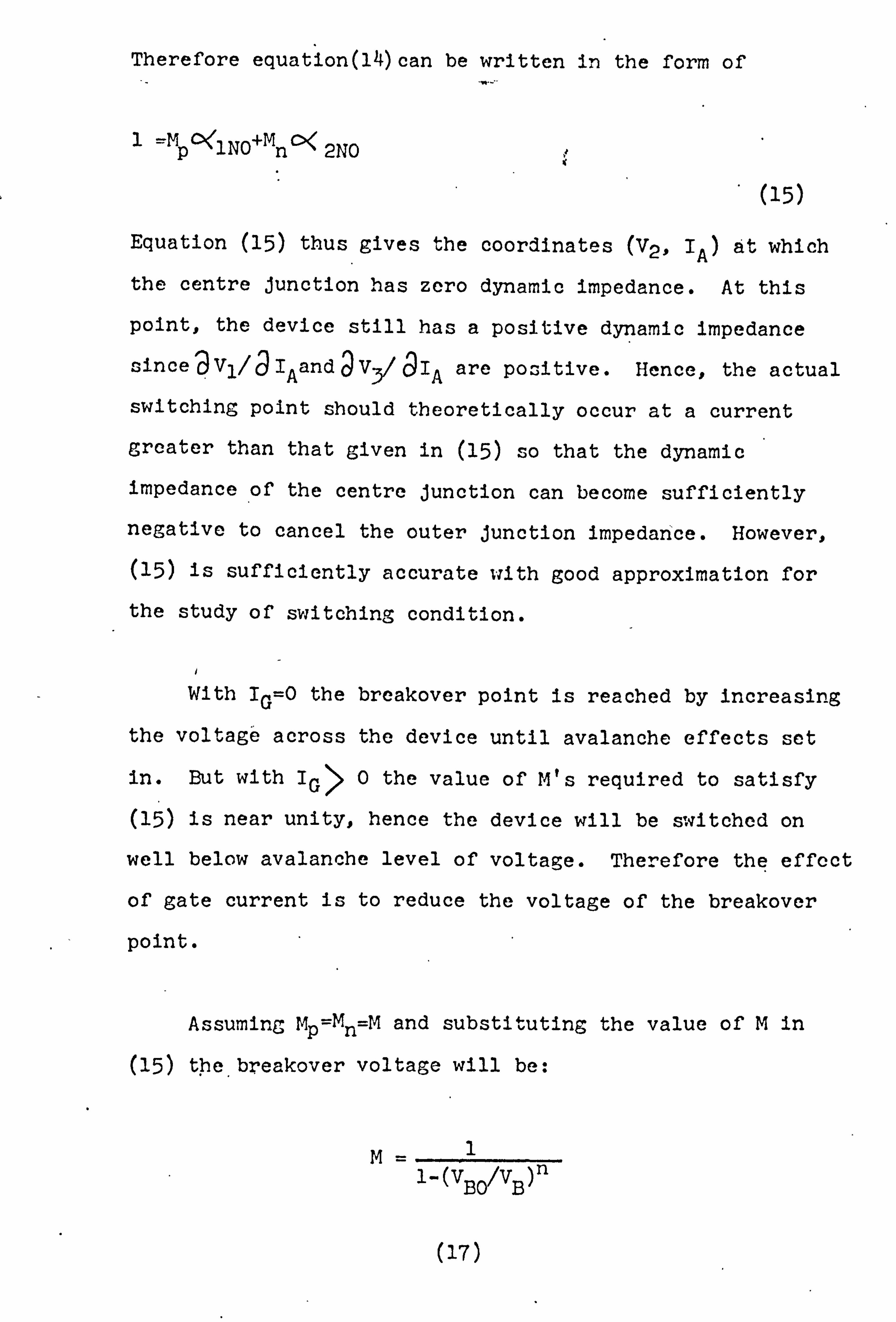
Therefore equation(14)can be written in the form of
mp 0ý1NO+I'lnc>ý 2NO
('5)
Equation (15) thus gives the coordinates (V2, A) At which
the centre junction has zero dynamic impedance. At this
point, the device still has a positive dynamic impedance
sincegVl/j A and ýV3/ aIA are positive. Hence, the actual
switching point should theoretically occur at a current
greater than that given in (15) so that the dynamic
impedance of the centre junction can become sufficiently
negative to cancel the outer junction impedance. Howevero
(15) is sufficiently accurate with good approximation for
the study of switching condition. C).
With IG =0 the breakover point is reached by increasing
the voltage across the device until avalanche effects set
in. But with IG> 0 the value of M's required to satisfy
(15) is near unity, hence the device will be switched on
well below avalanche level of voltage. Therefore the effect
of gate current is to reduce the voltage of the breakover
point.
Assuming MPýMn, =M and substituting the value of M in
(15) tpe_breakover voltage will be:
m1 1- (v
BON)
(17)
v 1/n - 130 z2
(1-C>ýlhT0 - £: ý9 21J0)
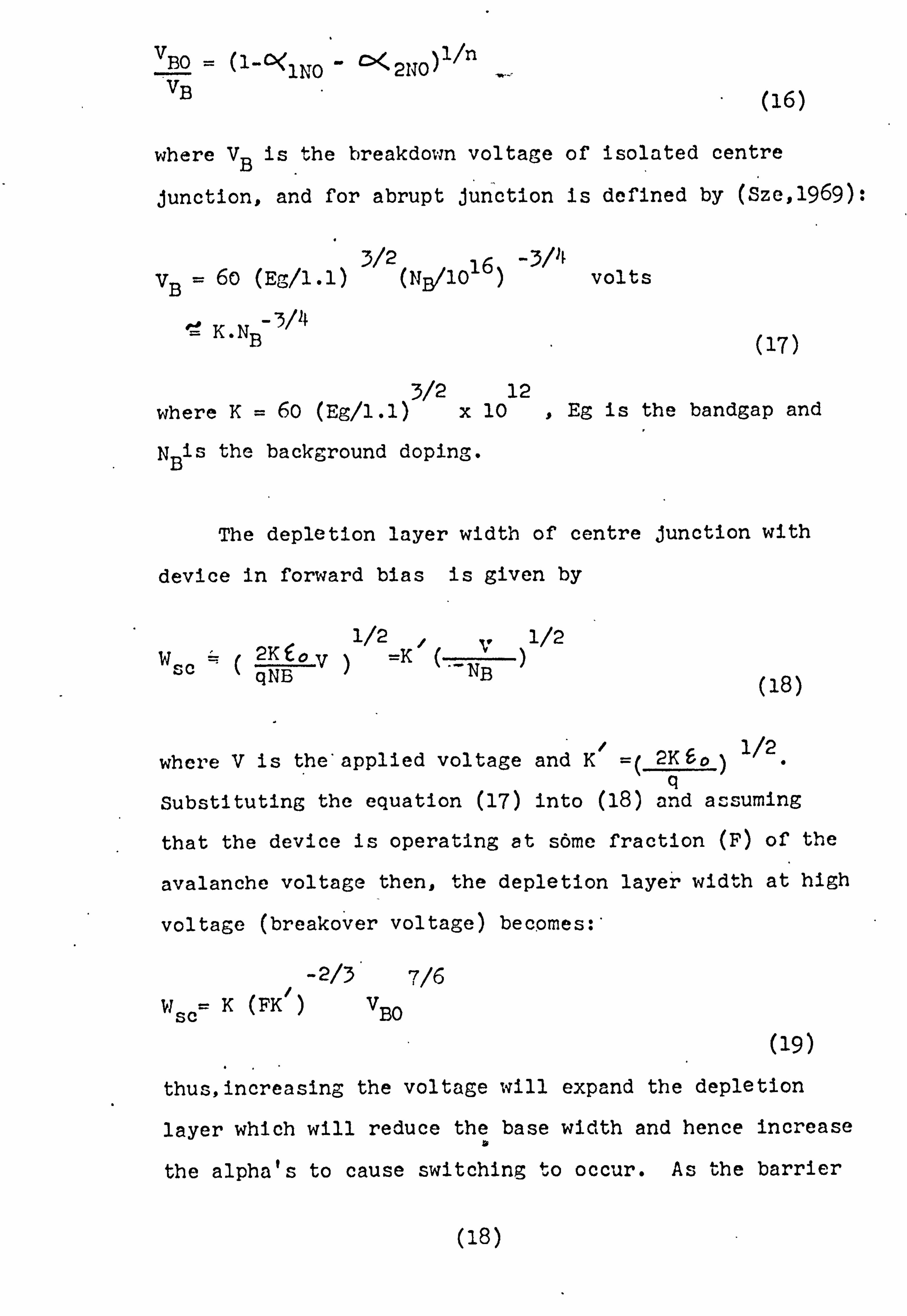
VB (i6)
where VB is the breakdown voltage of isolated centre
junction, and for abrupt junction is defined by (Sze, 1969)-.
3/2 16 3/4 vB= 60 (Eg/1.1) (NB/10 volts
'=' K. NB- 3/11 (17)
3/2 12 where K= 60 (Eg/1.1) x 10 Eg is the bandgap and
NB is the background doping.
The depletion layer width of centre junction with
device in forward bias is given by
2Kýo 1/2 V 1/2
qNB NB (18)
1/2 where V is t. he'applied voltage and K/ =( 2KEo)
q Substituting the equation (17) into (18) and assuming
that the device is operating at s6me fraction (F) of the
-he depletion layer width at high avalanche voltage then, t
voltage (breakover voltage) becomes: -
Wsc =K (FK -2/3
v BO
7/6
(19)
thus, increasing the voltage will expand the depletion
layer which will reduce the base width and hence increase ap
-o occur. As the barrier the alpha's to cause switching 1.
(18)

layer spreads through the base region to the opposite junction,
punch thrcugh effect results. Thus wider base width is
requaired in order to prevent the effective base width from 4
becoming zero.
(C) Negative Resistance Region.
At this region M nC5ý2NO +M pc'<lNO*>
1 and voltage across
the dVvice starts falling and eventually 14P ': " Mn= 1. At
the voltage very near V2 =0 the neglected [exp-ýP V2)-']
term is not negligible. Thus putting OM
=0 . in equation (10) 5V
and taking exponential term into account gives:
OV '-CýýMO- C'ý 2NO
e-/3V2_ /321S2 4- 9 V2
I, (20)
This is negative impedance expression near V2 =0 point,
since av 2
(d) The Forward Switched Condiltion.
In the ON state Mný--Mp=l and 10 (V 2) =0. The main
interest here is the total voltage drop across the device.
The effect of gate current is very small except near the
turn off point thus it can be neglected. Rearranging equations
4., 5,6 and putting Il=j 2 =I 3ý, A$
vl= ln si
Mný-Mp=l' one gets:
('9)
(21)

11 ( A2I'+,
) v 2ý -fi ln I; s 2
V3= P'ln (AýI +1 ýS3
wberep' nkT and: q
i- 0<� N 0<2I+ C><2N0<11-. ý51I -- 22
Al -« 1N 11 2NC<21 2
C><lN+2< 2N-1 2 2ý< O< 1-( lNC><lI- 2NC>'ý21
=
o< , 1NC41I+ CýýlN O'ý21- C<21
1-c' lN0<1I-C'ý2NC<2I
(22)
(23)
Al A21 In the ON state >> 1, in addition if -g2 IS2
>0 9
in order to satisfy equation (22) V2 should be negative.
This means that V2 must be forward-biased when the device
is in the conducting state. However, the total voltage
drop across the device can be written
+vl=ld [in AjAý
+ in IIS3 Vf-- Vl+ V2+v3
A2 'SlIS31 +v
(24)
where V is the voltage drop through tilt he wide base high
tivit resist .y regipn.
-y modulation in N occurs as soon as the Conductivil. 1 densit -y of injected carriers (holes) becomes comparable
with the original doping of Nl. This can take place in
the OFF state at values of current lower than the switching
current. The same conductivity modulation is responsible
(20)
I hhý - -- -ý, I
-he low voltage which is mentioned in the "ON" state. f or
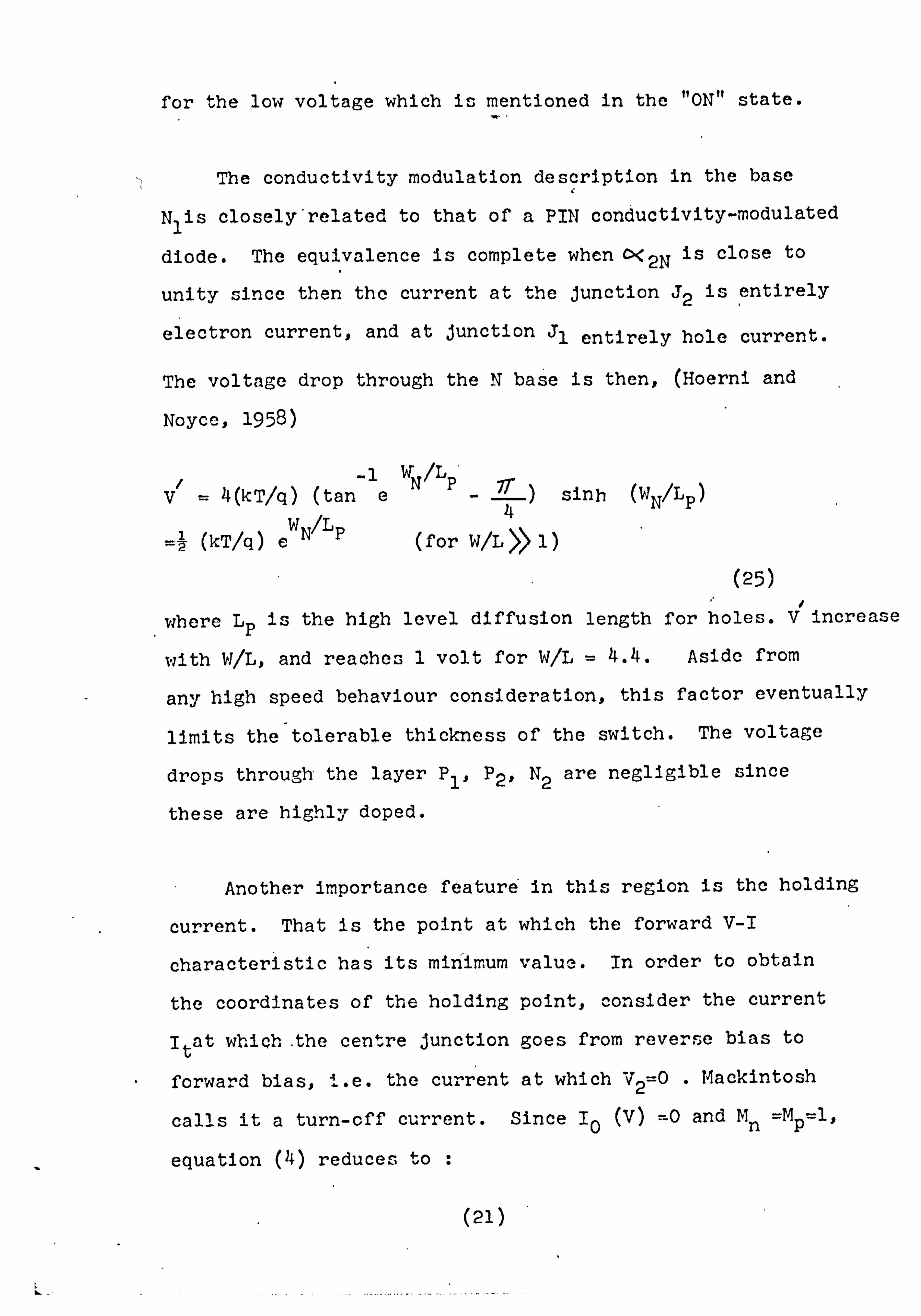
The conductivity modulation description in the base Ir
N1 is closely'related to that of a PIN conductivity-modulated
diode. The equivalence is complete when C5'ý2N is close to
-he junction J2 is I entirely unity since then tho current at t
electron currents and at junction J1 entirely hole current.
The voltage drop through the N base is then, (Hoerni and
Noyce, 1958)
.1 V- /L' v 4(kT/q) (tan- e
11 p- 7r sinh (WN /Lp) 4
(kT/q) eWN/LP (for W/L >> 1) (25)
where Lp is the high level diffusion length for holes. V increase
with VI/L, and reaches 1 volt for W/L = 4.4. Aside from
any high speed behaviour consideration, this factor eventually
limits the tolerable thickness of the switch. The voltage
drops throulgh- the layer Pl., P2., N2 are negligible since
these are highly doped.
Another importance feature' in this region is the holding
current. That is the point at which the forward V-I
characteristic has its minimum value. In order to obtain
the coordinates of the holding point, consider the current
it at wbich-the centre junction goes from reverse bias to
forward bias, I. e. the current at which V2 =0 . Mackintosh
calls it a turn-off current. Since I. (V) =0 and Mn =V--l'
'o equation (4) reduces t
(21)

1- (e-OV2_1) A('-Cýýljj-cýý20 -Cýý2NTG S2 O< IN o< ii+c< 2ND<2"! -'
therefore for V21--O and IA =It we have:
O< + C< + O< 2NId
1N 2N I
In a pnpn diode IG =0 so,
OZ. ldý C"ý2N
(26)
(27)
but in a pnpn triode, IG>0 there. L ore CýeN+ Oý2N <1 when
V2 =O. The current at which0<lN+4X2N 1-- 1 is then a point
in the ON r-gion, where the centre junction is forward CI
biased and previous analysis does not apply; the reverse is
true for negative 'G, However the condition V2=0 does
not give týe current at which dV/dt has its low voltage
zero. That is dV/dt=O point in-the low impedance region.
This corresponds to the minimum voltage point on the V-I
characteristic in the ON-state. Gibbons(1964) by setting
an idealized model showed that;
Ih = 2-5It
for a two terminal device
W. Fulop (1966) analysed the holding point by means
of zero bias at centre junction V2=0 and voltage minimum
(22 )

point (VM), that is dV/dt = 0, He pointed out that for
the direction of decreasing current and approaching VBO,
the precise location of the holding point is circuit dependent
and will occur where the circuit resistance approaches to
the numerically-increasing negative resistance of the
device. He also showed, that the WI point lies above in
current compared to the zero centre voltage point for a
given curve parametric in IGa nd this appears to hold for
positive, zero and negative gate current TG and agrees
with Gibbons' result.
High Injection Level.
A. Herlet and K. Raithel (1966) pointed out that the
forward characteristics of thyristor and PIN diode under
the condition of high level injection in both base regions
are completely identical if the width of swamped regions
is equal. The argument was that at high current the n-
and p base regions of the thyristor are so heavily con-
-ductivity modulated by the injected carriers that the
junction J2, vanishes as far as carrier concentration is
concerned. This is true for current above 10 amps. For
current below 10 amps, the argument was that the injected
carriers density is insufficient to swamp thep-base and
hence. V T . the total drop for SCR deviates from the diode.
They also showed that, the doping concentration in
the n base region has no influence upon this identity and
(2-5)

the quantitative behaviour of the forward characteristic.
This is perhaps because the high level lifetime's of injected
carriers are independent of conductivity and doping 17 -3 concentration up to 1.5 xlO cm in the P-base.
R. A. Kokosa (1967) independently proved the similarity
of characteristics of SCR's and PIN diodes. He used an
abrupt junction model, which included effect of carrier-
carrier scattering and emitter efficiency variation with
current density to calculate the potential and carrier
distribution of a pnpn diode in the base regions. H& also
measured thesc two factors by electrical and optical probing
techniques, and found good agreement between the calculated
and measured results. However the conclusion is that the
SCR above a current density of 1 to 10 amps Am 2 can be
ted as a PIN diode. treat
(24)
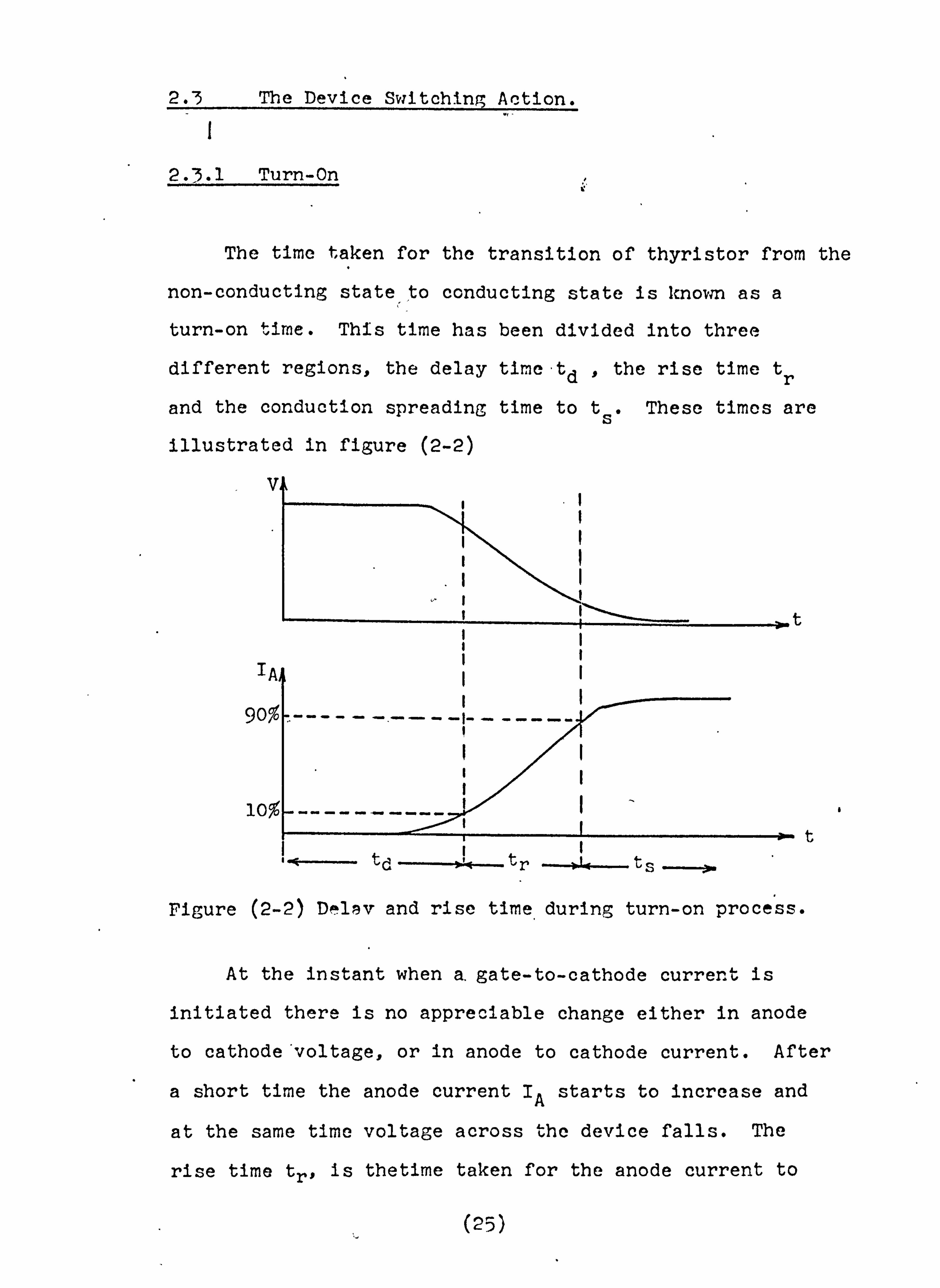
2.3 The Device Switching Action.
2.3.1 Turn-On
The time taken for the transition of thyristor from the
non-conducting state'to conducting state is known as a
turn-on time. This time has been divided into three
different regions, the delay t'm'c. td 0 the rise time tr
and the conduction spreading time to ts These timos are
illustrated in figure (2-2)
V II
K, t
I
90%
1
%[ 41 traI-
Figure (2-2) Dý-l*v and rise time. during turn-on process.
At the instant when a, gate-to-cathode current is
initiated there is no appreciable change either in anode
to cathode'voltage, or in anode to cathode current. After
a short time the anode current IA starts to increase and
at the same time voltage across 'Che device falls. The
rise time trs is thetime taken for the anode current to
I
t
(25))

increase from 10 to 90 percent of I A* The anode voltage
t4 continues to fall slowly, and the anode current to
rise, until a steady state value is reached after ts,
The delay ýime is the time during which charge is
being established in the device sufficient in magnitude
to support a current greater than the holding current of
the device. Once this charge ha's been established a
loop gain of greater than one prevails and the device
turns itself on. The rise time is the time during which
this takes place. V
There are several time constants contributing to the
a
delay time. Due to gate current flow the junction
injects electrons into base( P2)., and they begin diffusing
towards J2* It takes some time for these electrons to move
across base layer P2o This time is very short and given
by:
tw B2_ 2Dn (28)
These electrons will be collected by junction J2- In
order to maintain charge netrality, every collected electron
must be compensated by a hole injected acroSs J1. Again
another time is required for holes to pass the base region
so: 2-. Bl
ti 2Dp (29)
When they arrive and are swept by J2 into P 21 the-holes, cause
(26)

a further increase in injected electrons by J This 3* process continues until the current reaches its-steady
state load current level.
R. Davies, takes the lifetime of the carriers into
account and showsa more accurate expression for base
transit time which is
4W2 tt 2ý
)12D (11 4W Ift 772D (30)
where D is the diffusion constant.
Another contribution is the time taken to charge the
junction capacitance C3 of* junction J 3* This is given by:
VG C3(V) dV
0 t3 =j
'G (31)
where C3 (V) is the gate-to cathode capacitance, and is
a function of gate-to-cathode voltage V. Thus the delay
time can be the sum of three transit times which is taken
to conclude at 10% of the anode current,
t +t +4- 12t
The rise time depends on the geometric mean of the
transit . times of both of the transistors and is equal to
(Bergman., 1965).,
(27)
.tt 1/2
r C>'/' +c>< -1 1N 2N (32)
After the rapid rise time a small area near the
vicinity of the gate is turned on, causing the current
A to flow. The area of*conduction spreads simply by lateral
diffusion of minority'carriers from the turned on region
where their, density is high into the non conducting
regions during the spreading time ts. until the whole
cathode area of the thkristor is conducting. This
conduction spreading is associated with a drop in the anode-
to-cathode voltage of the device as the current density
decreases.
Different approaches were used for the calculation
of the spreading velocity. Longini and Melngailis (1963)
for a rectangular bar shaped thyristor, showed that:
F 110 D 772D 2
vsý-- ---( -F-+- N0F' 'a?
)
(33)
where 2F/ff is t -he flux of carriers that is fed to the OFF
region perunit thickness per unit length of periphery of
the ON region.
a is the thickness of each base
D is the diffusion constant of minority carriers
IC lis. lifetime of minority carriers.
In another paper, Dodson and Longini (1966) put equation
(33) in the form
(23)
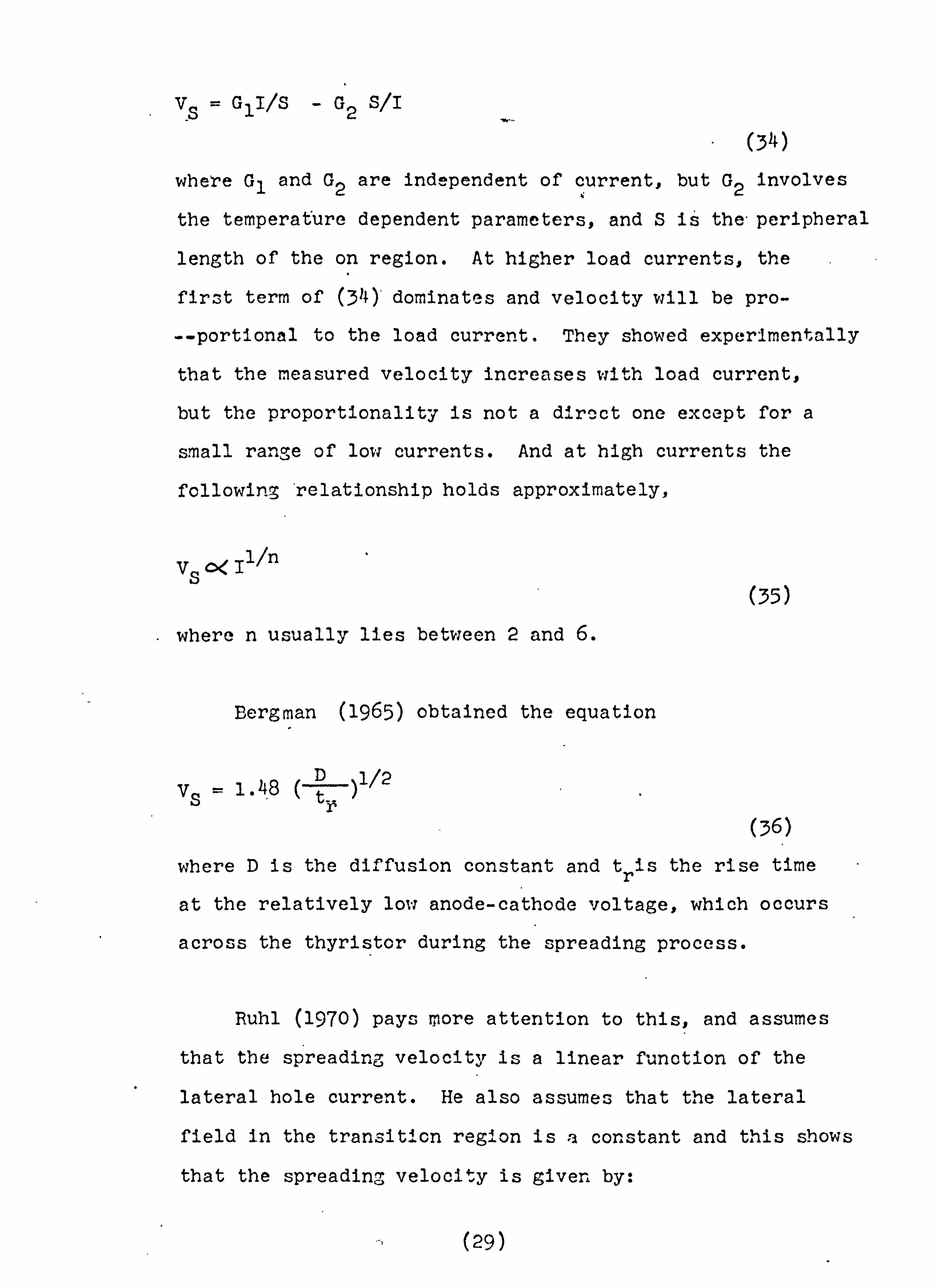
Vs=G, I/S -G2 S/I
(34)
where G, and G are independent of current, but G involves 22
the temperature dependent parameters, and S is the-peripheral
length of the on region. At higher load currents, the
fir, st term of (34)'dominates and velocity will be pro-
--portional to the load current. They showed experimentally
that the measured velocity increases with load current,
but the proportionality is not a diroct one except for a
small range of low currents. And at high currents the
following 'relationship holds approximately,
1/n
(35)
where n usually lies between 2 and
Bergman (1965) obtained the equation
1.4.8 D) 1/2 ty,
(36)
where D is the diffusion constant and tr is the rise time
at the relatively low anode-ca thode voltage, which occurs
across the thyristor during the spreading process.
RUM (1970) pays more attention to this, and assumes
that the spreading velocity is a linear function of the
lateral hole current. He also assumes that the lateral
field in the transition region is a constant and this shows
that the spreading velocity is given by:
(29)

0
S= AMk IT
in( jo
+ K) +C q Jo
(37)
where Je is the active area emitter current density, at
the edge of active region.
A is an unspecified function. independent Of Je and
temperature.
C is a. device constant independent of Je and K and
has a value usually near 1.
2.3.2 _____dV/dt
nroblem and the shorted emitter.
By applying a rapidly rising positive voltage to the
thyristor, it can be made to turn-on if the rate of rise
and magnitude of the anode voltage are sufficiently large.
This phenomenon can cause undesired switching of the device.
When the device is in the blocking state a rapidly
rising voltage applied to the anode lead will cause current
to flow throughJunctions Jl and J-3 and collector junction
capacitance C2. Since the. alpha's increase with emitter
current, the current which flows as a result of a rapid
change in voltage may cause the alpha sum to become unity;
switching then occurs. For rating and application purposes,
the dVdt capability of a devic e is defined as the maximum
rate of rise of forward voltage that the device will support
without triggering, at a specified percentage of the rated
blocking voltage.
Depletion of junction J2 due to the flow of holes to
(30)

the cathode and electrons to the anode creates a displacement
current which is equal to:
dC IMS ý-- C2 dV
+ V- dt dt (38)
The second term is very small In comparison to the
first term-and can be neglected. Its effect is to make
the current fall slightly with timeo because as the
depletion layer spreads C2 decreases. However (38) can
be simplified to
dV Dl S "': c2 --C717-
(39)
thus the dV/dt capability of device is influenced by the
capacitance of the centre junction.
The dV/dt performance depends on geometry (such as
effective base widths) and mostly on the lifetime of the
minority carriers. That means lowering minority carrier
lifetime will reduce emitter efficiency and transport
factor, which needs more displacement current to trigger
the device.
The performance with respect to dV/d+. can be improved
by negatively biasing the gate, as then the displacement
current can partly flow straight from the p-base and
across the gate, bypassing the n emitter, and thus not
(3')
releasing electrons from the n-emitter. Junction J3 is
then not biased in the forward direction owing to the
negative voltage from the gate applied to the p-base. 1:
Not until the desired moment of triggering is the gate
briefly positive.
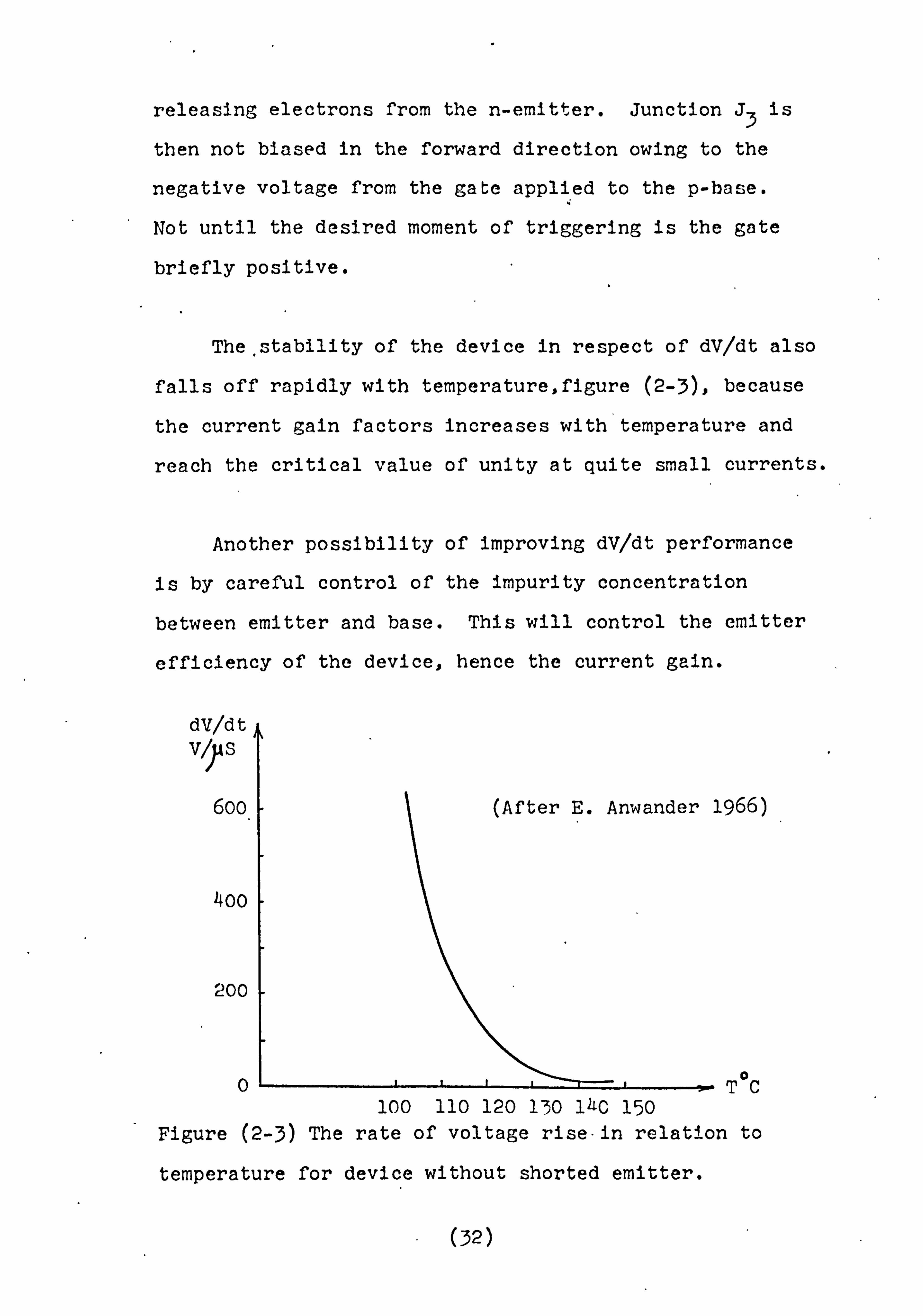
The. stability of the device in respect of dV/dt also
falls off rapidly with temperature, figure (2-3), because
the current gain factors increases with temperature and
reach the critical value of unity at quite small currents.
Another possibility of improving dV/dt performance
is by careful control of the impurity concentration
between emitter and base. This will control the emitter
efficiency of the device, hence the current gain.
dV/d t VIT s
6oo
4oo
200
0
1966)
0 TC 100 110 120 130 14C 150
Figure (2-3) The rate of voltage rise-in relation to
temperature for device without shorted emitter.
(32)

Emitter efficiency can be controlled structurally
by introducing shorting resistance between the under-
lying base region and the emittenfýgure (2-4)
G
J3
, 12
J1
Figure (2-4) pnpn with shorted emitter'
The primary function of"shorted emitter" is to reduce
the n-emitter efficiency at low current levels. In this way
the shorts serve to increase '%-, he high temperalture forward
blocking voltage capability of the device and also to
improve the dV/dt rating. They also provide a path for
the removal of stored charge from the p-base and increasing
the holding current of the device, thereby reducing the
time required to turnthe device off.
However with the anode biased positively, the hole
current collected at J. will flow laterally beneath the
emitter junction until the voltage drop reaches a sufficient
level (V 0) to cause J3 to emit electrons into the base region. -
Thus, we have an emitter which has essentially a zero
emitter efficiency at very low currents, but as the current
(33)

through the structure increases, the emitter efficiency
increases. The variation of'emitter efficiency with current
can be easily controlled by adjustment of the base sheet
resistivity and the spacing between shorted regions.
Aldrich and Holonyak (1959) used metallic contact
forming a short circuit between the emitter and adjacent
base region of the pnpn device and showed that, by varing
the shorted area it is possible to fabricate the device
with turn-on currents less or greater than the hold current.
They also showed that the holding current Ih changes
only alittle over an extensive temperature range, whereas
the turn-on current I BO changes appreciably with increasing
temperature. Also the breakover voltage remains relatively
constant, because of the small temperature coefficient of
avalanche breakdown.
C. K. Chu (1970) experimentally showed that the dVdt
performance not only depends on the shorted area but also
on the shorting pattern. By increasing the shorted area,
the distance between the shunts will be decreased and
actual dV/dt will be increased. He eliminated one row of
shunts around the gate, and observed that the dV/dt
performance was lowered and turn-on time decreased, but
on the other hand the loop effect could be minimized in
the forward V-I characteristic.
(34)

Raderecht (1971) approach was graphical and he showed
that., the degree of improvement depends directly on the
number and spacing of the shorting dots. A small number
of dots (i. e. 6) appeared to have'no significant effect on
the dV/dt capability or voltage performance of the device,
but as the number of dots was increased the dV/dt performance
gradually improved and the forward blocking voltage rapidly
increased to maximum and then a slight difference was
observed in voltage performance as the number of dots was
increased further. The interesting result was that, a large
number of small shorts was more ef f ective than few a large
shorts. The table below shows some of'the results.
I
No. of dots
Approx.
spacing of
Average VBO (volts)
Ave. gate firing
Ave. dV/dt
at 640 V& 0 dots chara. 125 C
thcu -21 0C 1250 C
fnA V I*GF/VGF V)IS
6 175 910 86o 64/1.4 23
12 125 1050 975 83/1.6 42
24 93 1060 1005 93/1.6 49
30 78 1040 1020 84/1.6 101
75 46 1060 980 lio/1.6 200
(After Raderecht, 1971). The size of dots were 0.027''
2.3.3 di/dt prcblem.
As mentioned previously the gate triggered thyristor
(35)

does not turn on over its entire-area immediately after the
f irst application of the trigger signal. Conduction is at
confined to a small area under the cathode which is physically
close to the gate electrode. The conducting state then
diffuses radially outwards with time from this initiated
point.
At thb. initial stage, if the power dissipated during
the early turn-on process is high and the initial conducting
area small, a large amount of energy will be dissipated in
the initial region. This causes rapid localized heating
and can re. -ult in the destruction of the device by excessive
temperature or thermal shock. A thyristor's ability to
switch into fast-rising currents without damage is termed
"di/dt" capability.
The energy dissipated per unit volume in the initiated
region during %londucting period is defind by (Cordingley, early
1971) Jtl
Ao. d (40)
where A(t) is the instantaneous conducting area, A(t) =
AO at t=O-
A0 is the initial conducting area.
d is the thickness of silicon slice.
E is the energy supplied per unit volume to the initiated
-er t seconds (t, <20ý S) point aft 1
(36)
P(t) is the instantanecus power dissipated in 1. -be silicon
slice, and is a function of the SOR's rise time.
A demand for power devices to be capable of turning
on into fast-rising high-current waveforms with low
transient-energy dissipation and without damage, persunded
investigators to work more closely at the problems involved.
However in-order to improve di/dt capability, Somos and
Piccone (1967) experimentally showed that decreasing the
initial thermal resistance from the conducting area to the
heat sink and decreasing the current density will increase
. the initial conducting area of the device which improves
its di/dt rating.
High voltage thyristors have inherently lower di/dt
capability, their crossover point Ia
point at which. at give n
current density, the heat generated in the cell decreases
, with increasing temperature and above this current density
the generated heat increases with temperature] is lower,
and for a given current density they have a higher conducting
voltage drop'. Hence for high voltage designs, to obtain
a di/dt capability comparable with low voltage designs,
the initial conducting area must be increased. This can
be achieved by alteration to the device's physical
geometry and increased gate drive.
A circuit solution to overcome di/dt (Maphan 1962)
was the use of saturable reactors in series with the device;
(37)

this limits the current after turn on. During the delay
period the turned-on area has time to increase so that the
current density is reasonably low when the bulk current
flows. The problem withasaturable reactor is that if the
current density is low during the reactor's delaý period,
the conducting region will not spread and all the current.
will still flow through one small area. Tberefore, the
designer of. such a circuit must consider the current during
the reactor delay period and the delay characteristics of
the reactor.
To solve the di/dt problem rather than circumvent it,
manufacturers have tried a variety of gating configurations
other than the simple side-fire gate. The centre-gate,
ring-gate and multiple-gate structures are theoretically
supposed to reach full area conduction about twice as
quickly as a side7fired device, but they have not increased
di/dt ratings appreciably. In these devices, just as in
the side-fired gate, more current is carried at the
initiating point than elsewhere, and local burn out is a
problem. However multiple -gate and ring-gate structures
require a large gate signal, or "Hard firing". Ring-gate
thyristors because of their long-gate cathode perimeter for a
constant emitter depth, suffered from reduced gate sensitivity.
In order to overcome this problem devices have been developed
that incorporate a gate amplification facility.
. Figure (2-5) illustrates the structure of the amplifying
(38)

gate thyristor. When the device is in the forward blocking Auxiliary K-
Primary Thyristor Gate
Auxiliary Gate
F1 and Cathod@
n nT L
p
n
p
+6A Figure(2-5) Amplifying gate thyristor.
state, the cathode of auxiliary thyristor is at the same
potential as the main cathode, and negative with respect
to the anode. Upon applying a positive voltage to the
primary gate, the auxiliary thyristor is- switched on,. and
the anode current starts to flow in the direction as in
indicated by the arrows figure (2-5). This lateral flow I
of anode current in the p-region acts as a very large gate
drive for the main-thyristor. Eventually the main
-hyristor is thyristor is switched on, and the juxiliary
switched off.
Cordingley (1971) showed that such a structure has
low switching loses and good di/dt capability with high
gate sensitivity at low values of gate drive. At high
values of gate current the amplifying structure has poorer
sf-iitching characteristic than a ring gate structure. This
(39)

is probably because the area over which the auxiliary
thyristor can dissipate the early swit--hing energy is small,
where as with the large ring-gate structure the whole of
the switching energy can be dissipated over a much larger
area and hence volume.
The amplifyJng gate structure as. well as the ring-gate devi(
havethe disadvantage that during the steady-state conducting
period the position of silicon used for the gating mechanism
is inactive. In this case at low frequencies and suitable
switching condition, the short gate device is to be-prefer-
red,, since it provides a larger effective area for steady
state condition.
The inverse gate thyristor has been developed to
eliminate the high gate drive failure. Figure (2-6) shows
the structure of such a device.
P. -p
i
J3
ii
Figure . (2-6) Inverse gate thyristor.
J4
(40)

Upon applying a negative voltage to the n3 rogion,
an ohmic current will flow from the gal. -e pulse generator
through the ohmic short common with the main cathode, across
the P2 region and back across the J4 junction. This causes
electrons to be injected from the n3 into the P2 region
building up the concentration of carriers under the junction
in the P2 region. This difference in carrier concentration
through the P2 region enables a current of diffusing carriers
to cross the'P2 region to be collected at the J2 junction
immediately beneath the n3 region. Switching then occurs
in this region. Before this point the J junction is 3 reverse biased. Once switching takes place at the J2 junction
in the vicinity of the n3 region. A large current typically
20 to 30 amps. is available to switch on the main cathode.
Thus a heavy current drive to the main cathode has been
generated so that the large di/dt (1000 A/ S) can be
absorbed by the main cathode.
Gray (1968) developed another gate structure device CO to improved di/dt capability. This device is called a
regenerative gate structure which is shown in figurc(2-7)
Regen. gate GK
Re--en. contact 0 11PIt
Initinl- I+ n, Gate %Regen. gate P2
n
P1
(DJA Figure (2-7) Regenenerative gate thyristor.
(In. )

Once the device is switched on, the current flowing
along the emitter produces a voltage drop. This voltage
drop in the "P"* lip acts as a signal generator. The
magnitude of the output voltage VO is equal to
Vr Vo ý R+r
(4i)
where R is-the variable resistance of the conducting area,
r is the emitter lip lateral resistance and Vr is the
anode voltage. This voltage which is positive with respect
to the cathode can be picked off the emitter lip contact
"P" and fed to point G, on the p2 base layer. This offers
the current an alternative path to the emitter contact with
a lower resistance. Thus most of the current will flow in
this direction and will provide a powerful gate drive G,
the regenerative gate. This current will turn the device
fully on. -Thus the regenerative action can improve the
di/dt capability. Multiple gates. were used successfully
with consistant firing at all of them.
2Q. 4. Turn Off.
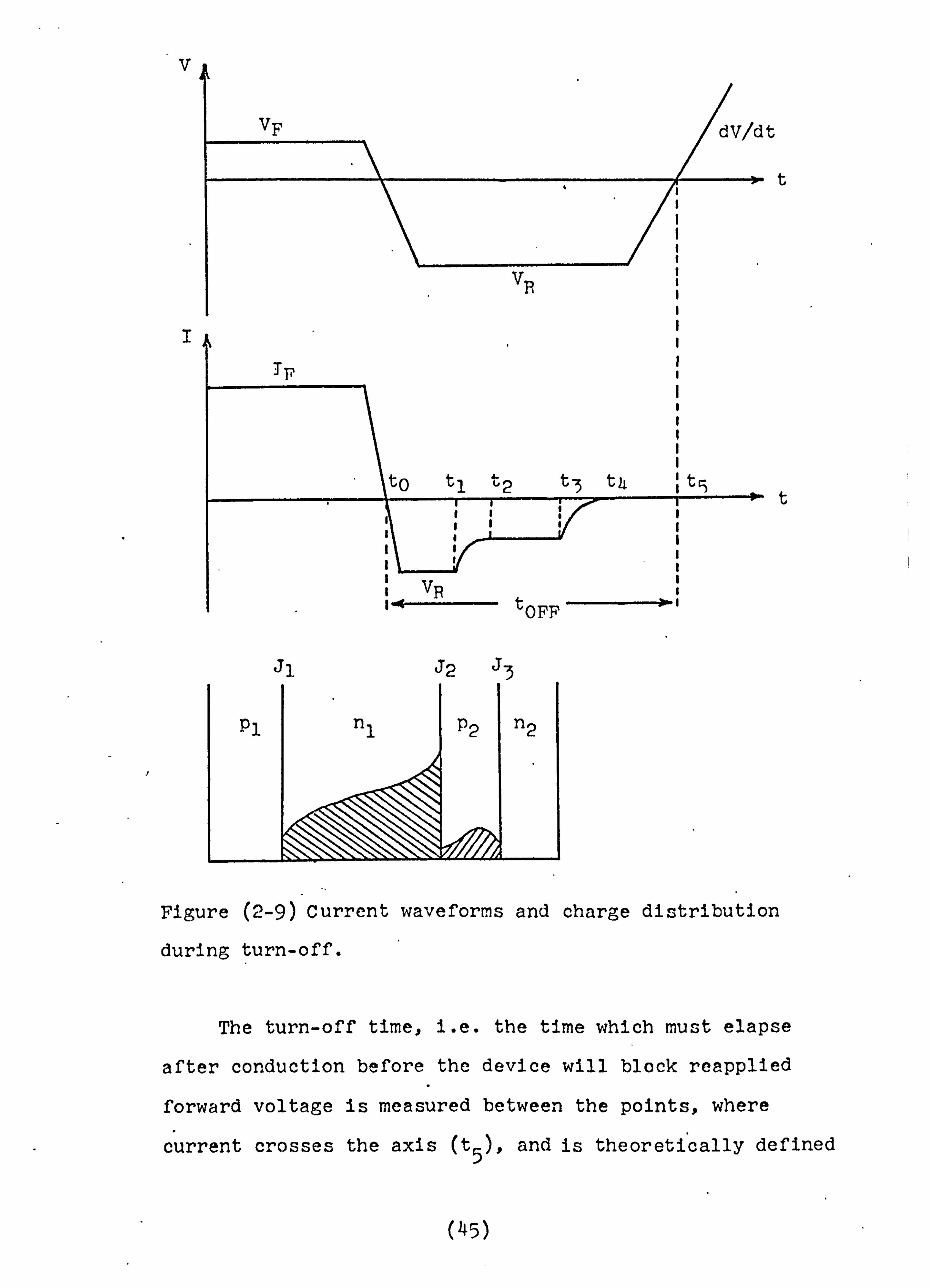
The turn off process is the regaining of the forward
-ermination of a forward current. blocking state after t
When the device is in the conducting state, all three
junctions are forward biased. Therefore both bases contain
excess minority carriers figure (2-8) which increase
with forward current. In order to turn off the device,
(42)

these excess carriers must be
an electric field byreversiný
decay by recombination. This
of base current from the gate :1 7
(D
removed from the bases, by
g the applied volt -age, or
can also be done by removal
contact. go- G
Figure (2-8) Charge distribution in bases in the conducting
state.
When the voltage across the device is reversed, the
junctions J, and J2 become reverse biased whereas the
junction J2 remains forward biased. Junction J3 because
of high impurity concentration on both gides., will have a
low avalanche breakdown compared, with the two other junctions.
Figure(2-9) illustrates the current wave form and charge
distribution.
A-I IV khe point just before tC) on the time axis the
device is fully on and carrying heavy forward current.
When reverse bias is a pplied, junctions J1 and J3 starts
collecting the minority carriers which have been injected
under forward bias. When the excess minority carriers
concentration at junction J3 reaches zero (time tl), its
-ion layer starts spreading and J becomes reverse deplet 3
(43)
J1 J2 J3

biased. The current through the circuit decays until. the
avalanche-breakdown of the junction is reached (time t2).
At this time the voltage across J3 has risen to its break
down value and the voltage across the device reaches an
avalanche value of J. The current through junction J2 30 during reverse recovery most -ly consists of hole current
injected from P2 into nl. Thus as holes leave base region
nI to J, and are swept into the anode emitter, other holes
enter the nl base by means of injection at Junction J2* On
V and the other hand as electrons diffuse across P2 to J, 3
are swept into the cathode emitter, only a small fraction
. of the base current near J2 consists of electrons injected
into P2-
Thus electrons are being swept out of base P2 by J3 at
faster rate than they are injected by J2. Therefore a much V
the regions R12, and n2 are sviept free of charge prior to
nl, i. e. the excess charge in the n1 base cannot be removed
readily but decays by recombination at a rate proportional
to the minority carrier lifetime. Furthermore because of
the lower doping and large width of the n, base, this region
has more excess charge to lose than the P2 base, and because
of this the turn-off time is determined primarily by the
charge decay in '. -he n base of a conventional thyristor.
However at tirre (t 3
). the excess hole density at J1 becomes zero.
Then the voltage across il begins to build-up, and the
current decays to its steady-state blocking value.
(44)
V
t
t
I
t
I' II
Figure (2-9) Current waveforms and charge distribution
during turn-off.
The turn-off time, i. e. the time which must elapse
after conduction before the device will block reapplied
forward voltage is measured between the points, where
current crosses the axis (t 5
), and is theoreti'cally defined
(45)
J1 J2

by figure (2-9):
'F tÖFF «": ý rp ln
H (42)
under assumption thatdV/dt and temperature effects are
negligible. In equation (42) 'Cp is the lifetime of the.
high resistivity base layer and IF the forward current
and 1,1 is. the holding current.
Equation (42) shows that the turn-off time can be
effectively lowered by lowering the lifetime of the
minori ty- carriers (holes) or by -increasing the holding
current IHI which may not be much help. For obtaining
good dV/dt performance, this parameter is already made
as high as possible.
Minority carriers lifetime can be controlled by
diffusing impurity atoms into thp base regions of the
device. In practice gold is a convenient impuritys
which acts as an effective recombination centre for
minority carriers (Bullis 1966).
Lowering the minority carrier lifetimeCp reduces
the Lp andwilllead to higher forward voltage drop of the
device. Wn may be'reduced to counteract this but then
V BO iY: Lllsuffer. Thus considerable compromise between
parameters must be tolerated.
(46)

An improvement in the characteristics may be obtained
if gold is diffused from the p1 side of the wafer, therefore
there is a fairly heavy concentration around J2 but small
along most of Wn This requires a steep profile. In this
way tOFF can be reduced without affecting LP to the same
extent as with uniform diffusion.
It waý already mentioned that the turn off process
can be achieved by removing the base current from the gate
lead, but this technique is limited to low currents or
specially designed devices. In the gate turn off devices
the carriers are removed from one of the base regions while the
device is in the ON state. This can be done by application
of reverse bias to the p-base (gated) region. Figure (2-10)
The removal of carriers will start from the edge of
emitter adjacent -to the gate contact; as a result., the
lateral 'base voltage drops.. causes junction J3 to become
reverse biased in the vicinity of the gate region and
therefore ceases to conduct current. Thus the gate current
will flow laterally through a base'resistance. However,
in this case, the anode current is determined by the same
external circuit current. Since the ON area has been
-he remainder is higher reduced, the current density in t
than when the whole device was ON. As more and more gate
current is withdrawn from the base " the region of cathode
emitter junction J at the vicinity of the gate lead finally 3
avalanches, with the result that a shunt path for the
(14.7)
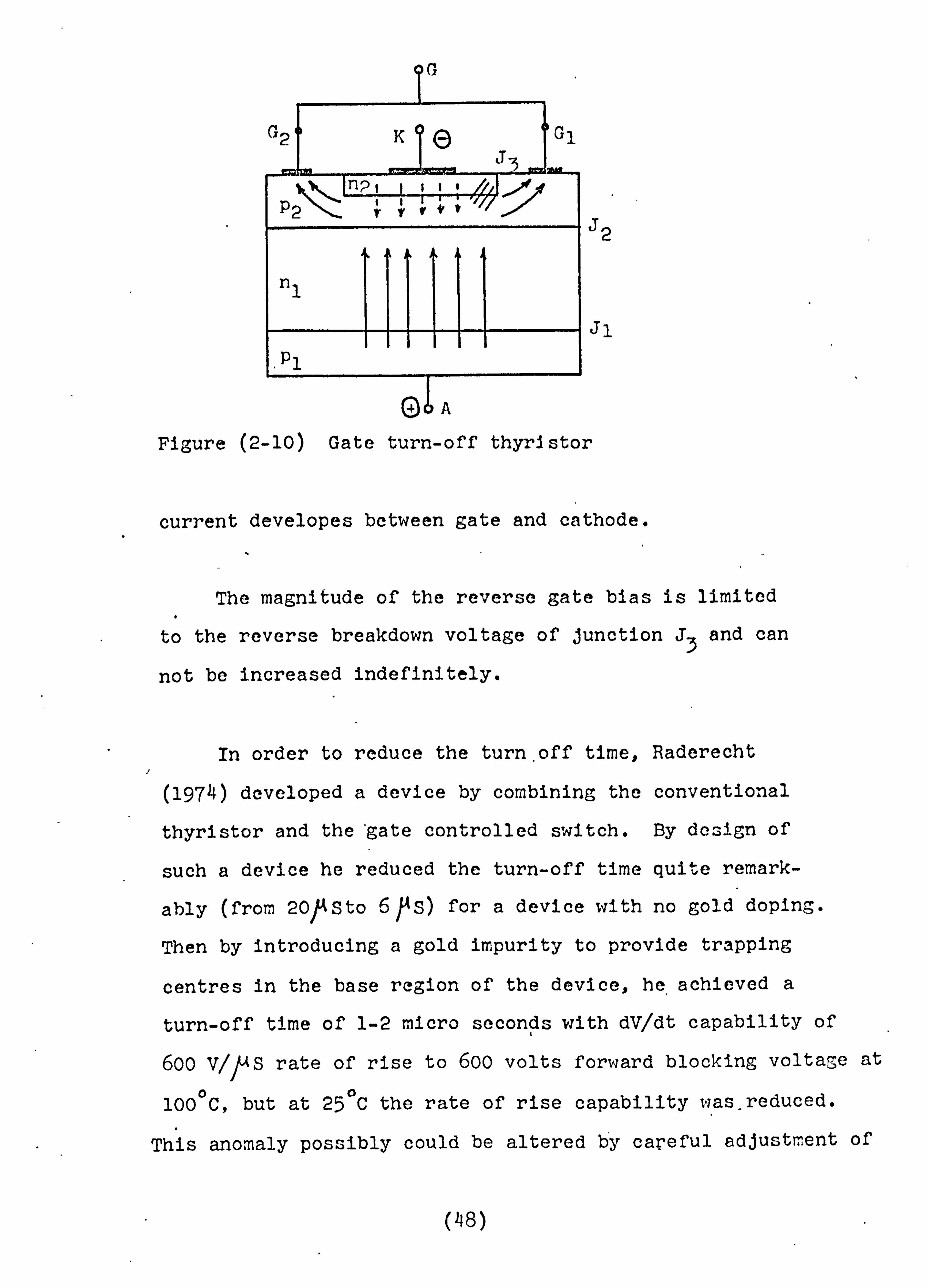
G
K E) 'Gl
allm-1 Inp
ni.
J1
P1
G)6 A Figure (2-10) Gate turn-off thyristor
current developes between gate and cathode.
The magnitude of the reverse gate bias is limited
to the reverse breakdown voltage of junction J3 and can
not be increased indefinitely.
In order to reduce the turn. off time, Raderecht
(1974) developed a device by combining the conventional
thyristor and the'gate controlled switch. By design of
such a device he reduced the turn-off time quite remark-
ably (from 20/ASto 6 PS) for a device with no gold doping.
Then by introducing a gold impurity to provide trapping
centres in the base region of the device, he achieved a
turn-off time of 1-2 micro seconds with dV/dt capability of I
600 V/, MS rate of rise to 600 volts forward blocking voltage at
100 0 C, but at 25 0C the rate of rise capability was. reduced.
This anomaly possibly could be altered by careful adjustment of
(48)

* the silicon resistivity and thickness or by introducing
metallic impurities 6ther than gold to reduce the lifetime
of silicon.
j
(49)
-I
Current Gain Measurement of High-Power
Thyristors.
3.1 Introduction.
The characteristics of the silicon controlled recti-
fiers is determined, by the two component alphas, i. e.
the current gains of the NPN and PNP transistor sections
constituting the PNPN configration of the SCR. Thus a
measurement of the two component alphas would appear to
be as important in the designo fabrication and commercial
manufacture of the SCR.
Several techniques are commonly employed in an effort
to measure the two component alphas of the thyristor. One
method consists of fabricating separately PNP and NPN sections
of the SCR and mepsuring the two component alphas by means
of transistor measurement. This. method deviates from the
desired degree of accurate simulation of the actual PNPN
configurationinthe measurements performed separately on
PNP and NPN sections and do not reflect the subtle inter-
play of gate, cathode and anode current flow in the device.
Another method of measuring current gains of two tran-
sistor section is by connecting a lead to each section of the
PNPN structure (Crees and Hogarth, 1963) and therefore measuring
the two alphas by standard techniques employed on transistors.
U tilization of the method is impeded by the inconvenience
(50)

and difficulty experienced in attaching a fourth lead to the
n-base region since the commercial SCR is a three-lead device.
However Fulop(1963) suggested a meth Iod
for alpha measurements on
the three terminal SCR.. treating it as a hook transistor.
His determinaltion was based on the idea of cut-off frequencies
of the PITP and NPIT sections which are not identical and
the alphas will have frequency characteristics from
which one will be able to measure the PNP and NPN alpha
values.
To represent the operation of the thyristor two
equivalent circuits will be needed,
a. DC equivalent circuit
From the two transistor analogue of the thyristor
can readily be shown the relationship between dc currents
flow and current gain factors, figure (3-1).
y Cl<
NPN
Ko !, ý2 P2 Nj TX
III
I=I+I IB2 TB1 = 'C2
B2 Cl G r__
11
----7 P2 F1 TA
TG I
PNP
Figure (3-1) Two-transisto-A analogue of PNPN switch.
A
I
(5]. )

The base current of the PNP transistor is I
IB I=
Cl-c: "<PNP) ', A - ICBO
(43)
wbich is supplied by the collector of NPN transistor.
However, the collector current of NPN section is
IC2 =C). eNPN'IK + ICBO 2
(44)
where ICB01 and I CB02 are saturation current of reverse
bias junctions of PNP and NPN transistors. The effective
. dc current gain of the SCR is given by
IA CýIdc IK
(45)
Neglecting multiplication at the reverse-biased
,, centre Junction and substituting equations (43) and (44)
into (45), noting that II the dc alpha willbe B C2
c>"ý - NPIT
dc - "-c><PNP
(46)
The dc alpha is measurable but to obtain the values for
Cýý Np and C: "< NPN we resort to ac values where a frequency P
separation of alphas will yield their values.
b. AC Equivalent Circuit.
(52)

If the dc currents are held cons. -ant at a fixed bias,
then a small signal ac current 3uperimposed on the cathode
current will causeasmall ac variation to appear in the
anode current. The small signal effective alpha is
defined as
04 a ek
(47)
where, i a and ik are the ac component of anode and cathode
currents. From combination of the equivalent circuits
for the two transistor sections, the small signal ac equi-
-valent circuit for PNPN can be shown as figure (3-2).
i I Ic Ko .f
.0
A
Figure (3-2) ac equivalent circuit of PNPN switch.
Ths- current at point A is continuous thus:
Cý. 4 pnp)
'a = C><npn
(48)
where 04 and o< are zmal. 11. si,,, P;, nal current gain facýors pnp npn
(53)

of the thyristor. From equations (47) and (48) we have:
CX C<npn
e 0/_ pnp
(49)
CK andc>< are limited by the cut-off frequency for npn pnp
minority carriers across the P and N base regions of 1. -he
thyristor. The frequency variation of alpha can be
equationated to (single pole approximation)
c< - OýnpnO
and ýý< O< pni)o
npn '+Jf/fn pnp - 1+jf/fp
(50)
wherec>< and c>e, are low-Afrequency small signal current pnpO npnO gains and fp and . 4'
n are cut-off frequencies for PNP and
NPN transistors respect -ively. Substituting equation (50)
into (49) we obtain:
npnO 1+jf/fn ýpnpO 1+jflf p
(5')
Since the base width of the PNP transistor is normally
greater than the NPN section, therefore the out-off
frequency of the NPN 13 higher than the cut-off frequency
of the PNP transistor. Figure (3-3) shows the frequency
variation Ofc><eo
At the low frequency plateau region A of figure (3-3)
the,. f <fp<fn-I therefore flfp<l but f/fn<<' thus:
(5, h)

Cý<npnO
e eO O<pnpO (52)
I-III 1- , 10.
O<
:ý Frequency
Figure (3-3) Frequency variation of effective alpha of
PNPN switch.
and is measurable. At the plateau region C. fp <f <fn
therefore flfp>>l and f/fn<<l thus:
=0enpnO
(53)
Hence from the experimental measurement, Oý, and C< eo npnO
are obtainable, andC<pnpo can be derived. Therefore the
small signal alphas for the two transistor sections are
known. At the frequency equal to the cut-off of two
transistors the effective alpha is equal to
f fn flfp>> 1
Cx ,e- Cýý npnO
D
(54)
(55)

f
c><, i C`ý'npnO
1- F2
flf" << I
0 if
(55)
As mentioned before the dc alphasc><PNp and 0<11PNO call
be readily defined from the ac values of current gains.
The dc current gains of two transistor sections are defined
by
Cý<PNP =II CP/ IAI and Cl< NPN '=
II 6N / IK'I
(56)
where. I CP and I CN are dc collector currents of the PNP
and NPN sections respectively, with the total collector
curýent (riven by C)
ICP I+I IC*N I
Thus to know dc current gains of two transistor sections
one requires to. know the ICp and I CN values. In order to
-ive alpha 'requency variation of effect obtain these, the I
should be repeated for a series of measurable IA values
at fixed V anode to cathode voltage. From this one AK
will obtain the alphas as a function of their relevant
emitter current.
4ý: ý cx (I and Q< (I npnO npnO K) pnpO ! --O<pnpO A)
(56)
Plotting the curve of alphas as a function of their
emitter current, and by integration from the definit -ion
of alphas, one obtains T CN and ICp,.,, thus:
r->< 'ý:: I ai
CN /a IK and npnO 'I
K Cý,, 4 dI CNn lb h, 0K
A ICP
0 Cl<
pnpO dIA
C>< I DT
pnpO ! 'ý CP/ 3 TA
(57)
and from the numerical integration of tbec<versus emitter
current plot. -O, one can obtain the separate dc. collector
-s, current II CN' CPI This makes a plot of the emitte. --
collector dc current of each transistor section possible
and thec>< PNP andO< NPN readily follow according to. equation
(56).
3.2 Method of Measurement.
The circuit employed is shown in figure (,, ý-4). The
small signal anode and cathode currents ia and i. respectively
were measured on an oscilloscope (later by sensitive valve-
voltmeter) and the ratio of i, , /ik was plotted as af nction c
of frequency.
-04 e=ia /i
k=
va /R Ava
%ý -/R,
V. - K 1% K since RA=RK=5.7 -Jl-
Signal level of the order of tvlmV across the 5.7 ohms
(57)

dlk. ' el
OM ein IN,
i 7 e
db 4ah

resistor of the cathode was employed. In order to got
such a signal level across the cathode resistor a signal
of order 3.0 mV to 15 MV was c-. nployqd at the cathode
-gate terminal. This variation of applied ac voltage
was dependent on the size of the device. Therefore in
comparison with the dc signal, the ac signal was low
enough to call it "small signal". 5 Watt 5 Watt
500" 500-A-
1 0.1 )IF 5.7-fl- 4,, lpF o-11T"
JIF pF VAK
"ik 1000 100.0
--8)IF 0-350 V
A. C. 4Do v 4r, c v 650 V
ra G. 1(67-fL 5.7-rL
0-50 V
I'
I
Figure (3-4) Oircuit used fw current gain measurements. .
A variable inductance L AG between the gate and anode
was employed to tune oult'. * the unwanted feedback due to the
-re junction capacitance at high frequencies (above cent
100. KHZ) to show up the decline of the second plateau.
At high enough frequencios, the reverse biased junction
capacitance acts as a parallel path to the anode current,
shown in figure (3-5).
( 58 )

0
0-111 mH
II
I Figure (3-5) High frequency equivalent circuit.
The upper Pn junction has a Very low impedance as
it is forward biased. The dominant term is the capacitanpe
C and reverse biased Junction capacitance. C has a
very low impedance at high frequency. However, at low
frequencies, capacitance C has very low admittance , hence
ic is very low and negligible compared to "a. Thus the
effective alpha is
a~ a e. ik 'k
where 'a true anode current.
At high frequency ic is not negligible because of the
lowered imPedance of the C. Thus
(59)

Iii ia ia a- c 'k ik::
/ 'k
Hence 'ic of' i to i at high frequencies, by taking the rat ak
the obtained value for the effective alpha will be high.
However the inductance L AG will*tune out this capacitance
and therefore ic will find no path to by-pass and the
obtained alpha will be near the true value. However it should be
remembered that in this case the cut-off frequency obtained
for C5'ýnpn is not a true value -because the emitter-base
capacitance will be tured out at the same time.
meamirements:
A number of devices were measured and some details of
their design where known are shown in the following table.
Device Slice
No. diameter
Slice
thickness
Depth of P diffusion
Width of 4-'
n type base
V BO 'peak cal. 4-
-onp_u ClIn J, m )i m )i t"i KV A
_ KHZ
1 1.8 175 37 100 M 116 39 2 3.7 450 P, 7 275 2 500 5.1 3 3.7 1625 200 625 6 1000 1.0 4 not 0.5 10 --
%u-doped 5 0.5 10 A u-doped
TABLE (1)
The calculated values of f(pnp)t were obtained from,
(60)

Pritchard (1952).
1.22 Dp r(pnp) t2 Y Wn
which assumes a purely diffusive minority carrier transport
across Wn with a diffusion length LP>> 14 n relating in an
approximate triangular excess carrier concentration profile.
A value of order 10 cm2 /sec for Dp was assumed. These
conditions may well not prevail and part of the small
differences between f (pnp) t and their measured counterparts
could be due to this.
3.3.1 ___Device
No. 1
The measuredc>< values versus frequency for anode-to e
-cathode vOltagOs VAK = 50 V and 200 V are plotted in
figures (3-6) and (3-7) for a number of anode currents.
Also the calculated value of c::, < and c>< as well as . pnpO npnO
their sumc: ýe are shown in figure (3-8) plotted as a function to
of I A*
This devicep in spite of its relatively small Wn
shows low0e lues. This could be due to a very low pnpO va
. lifetime in the n base. The value of CK to increased with
-V and I values it VAK and IA but even at the highest AK A
is still well below the critical value of unity.
The anode-cathode dc-current characteristics of the
(61)

thyristor is showrY in figure (3-9). However for 200V V AK
the device was found to switch at 22 mA. The calculated
7C(pnp)t value agrees reasonably well with the measured
value of f pnp according to equation (55).
- From the above curves and by utilizing equation (57)
one can readily calculate the dc collector current of the
NPH and PNP transistors (I CN' I CP
) respectively, and hence
the de current gains of two transistor sections. At the
point near the switching the values of I CN and I CP are
equal to :
cli 0ý dI
npnO K and C>l dI IIAI cp pnpO A
ICN ý 19-38 mA and
where
ICp =1-5 mA
VAK 200 V and IA= 20 mA
'A (cal. ) =I CN +I cp ý 20.89 mA
Comparing the calculated value of IA with value of
A directly obtained by measurement (20 mA) shows favourable
agreement. Thus from th-'r, the sun of dc alphas can be
calculated, which is well below unity.
0.4 +0., / o. 42 PNP NPN :;!
(62)

whereas at this point the su! n of small signal alpha is
considerably closer to unity.
C: ><to = 0< + r->< = 0.74 npnO pnpO
- This confirms that it Is the small signal alphas which
control ',, he switching point.
3.3.2 Device No. 2
Valul2s O: C VAK 10 and 50 V were chosen and the measured
values ofcý, e versus frequency are shom plotted in figures e
(3-10) and'(3-11). Figure (3-12) shows the values of'cý'4pnpO
and c>e versus I as well as C, This device although to- r npnO 'A
it has the same slice diameter (3-7 cm) as device No. 3..
-s much smaller n base width W value has in keeping with it Vn
much higherc$npo and fpnp values. There is reasonable
agreement between f(pnp)t and measured f pnp "aluez'
Figure (3-13) shows the de anode-cathode characteristics
of the device. This device switches at TA = 10 and 12 mA
for VAK " 10 and 50 V, respectively, and 0< to is seen to
be very close to unity near these values.
For this device the calculated value of de collector
currents 'CNI ICP from the corresponding curves are:
Ici; =0 .5 mA and iCp = 6.2 mA
(53)

wbcre VAK = 50 V and IA= 10 mA
therefore the calculated A value at the point near the
switching is equal to
,A (cal. ). = I CN +I Cp ý 11.2 mA
which with a 10% error compares favourably with the value
of 10 mA obtained in direct measurement. Thus the sum of
dc alphas can be obtained, which is ttill below unity.
r->Z + 0ý - -- o. 81 PNP NPN
where as at the same point the sum of small signal alphas
is somewhat closer to unity.
C)-e CK + ý>< to npnO pnpoý-- 0.96
I This again shows that the sum of dc alphas is lower than
sum of small signal alphas at switching point.
3.3.3 Device No. 3
This device like device No. 2 has a slice diameter
of 3.7 crm but is capable of withstanding 6KV with a
corresponding large Wn value. Figures (3-14) and (3-15)
show the effective alpha O. 'e values as a function of
(64)
frequency for a number of anode values with V AK --:: 50 and
200 V respectively. Figure (3-16), shows the calculated
Cýý and CX as wel pnpO npnO
as a function of IA with
reasonable agreement was
fpn*p-9 it was-not as good
being the-wide n-region,
asc><, the sum of alphas plotted to v AK as a parameter. Although
obtained between f(pnp )t and
as expected. The% reason for this
which will yield a higher f pnp*
Theo< values are comparable with those obtained npnO for device No. 2 but0e
pnpO is, because of the much wider
W n' considerably reduced.
The dc-anode current. as a function of cathode dc
current is shown in figure
The dc collector currents of npn and pnp transistor
sections (I CN $ ICp) were calculated according to their
respective curves and from this the dc current gains. '
'CN ý 18-36 mA I CP' = 3.2 mA
'A (cal. ) =I CN +I Cp = 21-56 mA
where VAK = 200 V and 'A ='20 mA.
This again shows reasonable agreement between calculated A
and measured I A' So the dc sum alpha will be:
C>/- + C>1, =0 . 33 NPN PNP
(65)
This is lower than small signal alpha sum, because at this
point c4 to is equal to
c>4 C>/- + C; 4 0.49 to npnO pnpO =
Once again this shows ýhe dominant influence of small
signal alphas in controlling the switching point.
3.3.4 Device No. 4 (Not Au-Doped)
Measuredc>e values versus frequency for anode-to- e
cathode voltage V equal U AK to 50 V is plotted in figure
for-a number of anode currents. The calculated
values po and(D-e and their sum are shown in 0n npnO p figure (3-19) plctted versus A the anode current.
-he The anode-cathode dc current characteristics of
small not Ati-doped 10A thvristor is shown in figure
20). The slope of this is C*<'eo and agrees'well with the
measured value at one point. For 50 V anode to cathode
voltage the device was found to switch round about 3.5
mA.
Once again t, he calculated values of I and I ICN CP
were obtained from corresponding curves, and reasonable
agreement was found between calculated IA and mea., -: -, ured
one -
(66)
'CN ý- 2.8 mA and lCp ::, - 0.3
where
v DOV and AK IA 3mA
&0 ,A (cal. ) ICII + ICp == 3-l. mA
The sum of dc alphas at this point near the switching
is
PIP + C>< NPN7 0.45 c-
which is below unity.
where as at this point the sum of small signal alphas is
not far from unity. A
CII/ + CK t-- 0.90 pnpO npnO
3.3.5 Device Fo. 5 (Au-Doped)
This device is nominally identical to device No.
except that it"was gold doped. This is in ordcr to reveal
the influence.. if any., such doping, might have on the current
gains as well as the known effect on switching speed. The
value of V AK = 50V was chosen and the measured valueS of
o<e versus frequency are shown plotted in figure (3-21).
Figure (3-22) shows the values ofO-ý and O<npnO versus pnpO
(67)

'A as well asc., /to the sum of alphas. The effect of gold
doping onO< pnpO is particularly pronounced. 7his value
has been depressed because of the considerably reduced
lifetime in the wider ungated region. However, figure
(3-23) shows the anode-cathode dc current curve of such a device. For this device' the switching current found to be
10 mA at VAK = 50 V andcXt, is seen to be 1rery close to
unity near this value,
For this device the, calculated values of dc collector
currents I CN and I CP from their respective curves versus
emitter currents at point near the switching are
, 8.2 mA CN
where
VAK ý 50 V and
therefore the calculated A will be:
lCp ý 0.45 mA
,Aý9 mA
A (cal. ) I CN + Icp = 8.65 mA
which is in reasonable agreement with measured I A* The sum
of de alphas at this point is
C>el + C>< = o. 49 NPN PN
whereas the sum of small signal alphas is very close to
-his point. unity at 1.
(69)

cllý = C>< + CK to npnO pnpO = 0.92
This once again confirms that it is 'the small signal alphas
which control the switching point.
3.4 Discussion of Results.
The manner in which the devices were measured showed
that the Fulop method (1963) originally employed for the
measureMent of small current gain factors can be successfully
applied to the measurements of high-power thyristors,
provided that certain precautions are taken with the
measuring system. The method ensured that the centre
junction wa's-reverse-biased and the outer junctions were
forward biased. The thyristor is therefore in the high
impedance domain and dc anode current IA is varied by
varying the gate forward bias on the p-type base P2* I
The measured values ofc>,, ' andc>< together with npnO pnpO the values of fpnp and fnpn would be expected to yield
some qualitative, if not quantitative, information on the
dimensions and material properties (lifetime, doping profile,
etc. ) of the thyristor. By repeating these measurements
at a number of fixed current levels, the dc component of
currents. in the separate transistor sections can be cal-
-culated and 'from this the dc current gainso<NPN ando<pNp
can be readily obtained. It was found that the
(69)

C>< to ý- Cx npnO + O<
pnpO were near unity at switching of the
thyristor. But at the voltage similar to that applied
to measure the small signal current, gain factors the
sum of dc current gainsc, < NPN + C>< PITIP was found well
below unity. This shows that, -it is the small signal
alphas that. control the switching point rather than dc
alphas. That means switching occurs wben
CýýnpnO + Cý<pnpO
In a fuller investlgaý, ion of the switching process
In high-power thyristors, consideration would need to
, be given to the degree that the two-dimensional or lateral
aspects of'. these measurements on these large area
thyristors play a part. Emitter fringing of the cathode
due to lateral gate current flow in the p-type base would
be a case in point and here the influence of the shorting
dots in the cathode would be interesting to evaluate.
The currents flovtin, -, in the above measurements are
admittedly small but apart frorn the low value Of VAK, not
all that far reemoved from the switching condition. In
fact 'A was increased as far as permi-asible without
switching the device.
W. C. Un (1974) proposed an automatic system for
measuring small signal current gain factors of thyristor.
His method is much faster and also 'accurate than hand
plot method.
(70)
The Current Gain Temperature Dependence
in Thyristors.
4.1 Introduction.
From early papers one gains the impression that the
effect of temperature on thyristors is to. degrade their
voltage blocking characteristics, quite remarkably so in
some cases. This was shown by Smobyanski (1963). In many
cases the degradation is due to increased surface leakage
current which is very sensitive to temperature.
One of the important effects of temperature is to
increase the saturation current of the reverse biased
junction which increases the two alphas of separate sections.
Another effect is that the injection efficiency of emitters
ý increases with temperature because of the rapid increase
of diffusion components of current compared to the recombinat
ý- generation component with temperature.
Raderecht and Hogarth (1964) did measurements on four-
terminal SCR's investigating temperature dependence. At low
currents the variation Of"ý<npn will depend largely on the
variation of emitter efficiency which increases as temperatur
rises. 'ý'<`pnp which can be shown to be /-3t at this level
of current also increases with temperature. At medium
currents there is small change of c<npn with increasing
temperature which is ascribed to a decrease of resistivity
of the p-base canally not a tendency for the diffusion
length of holes in the emitter region. (71)

But'o<pnp remains fairly constant or shows a slight increase,
due to 1. -he increasing transport factorp., as the temperature
increa. ces. At high currents due to the dominant effect of
resistivity of the*base on diffusion len'gth of minority
carriers, the emitter efficiency henceoý, will decrease npn
as the temperature rise, -ý. 0< will remain small and pnp fairly constant over a range of temperature because the
emitter efficiency decreases with current and temperature
since the transport factorp increases as temperature rises;
thereforec'$'np depends on two opposing trends.
Buhana (1969) investigated the temperature variation
of current gain of transistors. He showed that lifctim.
'Cb varies as ni 2
and thus as T3 e-Eg /kT.
The transport
factor is given by
sech W
Lnb
(58)
and
Lnb ý'- FDrýb 'Cb
The decrease Of Iýnb with increasing temperature which is
caused by increased lattice scatterIncr: "), will compensate by
increase of"C. with temperature. The overall effect on L 3 nb will be an increase with increasing temperature and therefore
of /I with temperature.
In his paper he ClAimed thata heavy emitter causes a
(72)

decrease of energy gap Eg due to lattice stress. This is
because at high doping levels lattice deformations and
dislocations produce a change in energy gap. This in turn,
leads to a different value of n in emitter than in base. i
The emitter efficiency expression for an NPN transistor
corrected for the effect ofA E becomes:
1+ (Dpe/Dnb) (W/Lpe) k exp( L6E/kT) (59)
This introduces an exponential temperature dependence into
the expression. In thyristors the only emitter which may
have such higher doping in N2 region, therefore ýNPN shows
- this effect in some devices.
4.2. Method of Measurement.
Measurements of current gain values were made by the
method described in the previous section. The thyristor
Ywas placed in an oven with a temperature controller and
also an electronic thermometer with a copper-constantan
thermocouple which was used to record the device temperature.
Temperature was checked during measurements with an accuracy
of + 20C.
Measurements were carried out on devices as previously
employed (table 1). For a given constant temper&ture
reading, the usual voltage anode/cathode ratio was taken for
various frequencies of the small ac signal between 500 C/S
(73)

and 500 KC/S. The dc conditions were set by measuring the C3
anode-cathode voltage V AK and anode current IA The anode-
cathode voltage was kept constant and the readings were
repeated for a number of different anode currents up to
permissible current values. The temperature setting on
the oven was then altered and the whole series of experiments
was repeated at the new tempcrature setting.
Switching parameters were then recorded over the range
"0 0C to 1600C except for device No. 5 Por of temperature, 12 1 0
which measurements over the range of 20 to 200 C were made.
4.3 - Results.
Figure (4-1) shows for device No. 1 the variation of
0-e and C>< with temperature at a number of fixed npnO pnpO
ancde currents. The sum C-'-<to 0< npnO + C<
pnpO is also
plotted and from this one can derive the variation Of 'BO
the breakover current, with temperature; I BO is defined as
a current through the device at the point of brealcover
under two-terminal operation and is governed by the conditicn.
O-e to = 1. Therefore the curve I BO
(T) as a function of
temperature is the locus of all pointt as T is varied for
which'to =1 at of course the prevailing breakover
voltage V BOO
This can be closely simulated under three-terminal
operations, and at a considerably reduced voltage
(74)

compared to the two terminal breakover voltage V BO 0 by
moving along a line of constantO<tO, such as is plotted
in figure (4-1), as close to unity ajs possible.. Observing
the intersection with curves plotted for constant IA I it
will be seen that initially curves of decreasing IA values
are intersected and thcn as temperature increases further,
increasing IA values are intersected. Figure (4-2) shows
the measured I BO values plotted versus temperature and
this confirms the trend predicted from figure (4-1).
Gate firing current 1 G"s found to decrease linearly as
thetemperature rises. This was expected since the generated
minority carrier current increases with temperature,
therefore IG for a fixed IA should decrease. Thin is
shown in figure (4-3). The variation of breakover voltage
v BO decreases with increasing temperature, as a result of
injection due to increased current carried by junction J 2*
j For devices Nos. 2,3,4 and 5 the correspondirg curves
are shown in figures (4,00-6), (4-7) , (4-8), (4-9), (4-10)
(4-11), (4-12)1(4-13) (4-14), (4-15) and (4-16) respectively.
Once again the effect of gold dcping emerges frcm figures
(4-11) and (4-14) which are for two nominally identical
small thyristor; (10A) except that one is made from
deliberately gold-doped silicon.
(75)

4.4 Analysis of Instability of pn]2n deviceso
It is well known that the small signal low-frequency
alphas which forc,, ' to - Cx + o< npnO pnpO
l, determines the ý
point of instability. We shall now discuss some aspects
of instability. In particular we are interested in what
role the variation ofc>< andcs< with temperature npnO pnpO and anode current play. We shall assume multiplication
to occur across the central reverse-biased junction and
for mathematical convenience shall put MMM where nP Mn and Mp are the multiplication ratioes fcrelectrons
and holes respectively. Also to put the operative transistor
section beyond doubt we write for the large signal alpha
of the npn sectionWNpN and that for the pnp section, cý'<PNP*
For the anode current I we have therefore A
Me C' , Ný PNPIA + Mc NPNIK + MIcO + 'Dis
(60)
where 1K =IA+ IGO 1K being the cathode current, IG the
gate currento IC0 the saturation current of the isolated
reverse-biased centre junction, and I Dis is the displacement
I or capacitive current flowing due to a rate of change of
voltage across the depletion layer capacitance Ciof". 'he
centre-junction.
This can be writ'.. -en as
I' d (C V) Dis dt j
(70' )

where V= voltage across the centre junction which to a
good approximation is the total applied voltage.
From this it follows that
M(C>ýIPN'G _+
Ir, 0) + Di§ ,A =-
O< 1-M( PNP + C"%NPIZ)
(62)
Thus A is not only the dc current but may also contain
(large-signal) transient due to IGM or I M13-0
-ter current of Considering IA as the large signal emit
the pnp section with a corresponding collector current I CPO
and similarly for the npn section IK and ICU, then clearly:
CP +I CN (63)
Y ICN ýý- mo< NPN IK+MI pOn +I Dis
(64)
M oe I+ MI CP PNP A COP
(65)
where I00 ý: I cOn + Icop are the electron and hole current
contributions coming respectively from the p and n type
case and I Dis has been arbitrai-ily assigned to the npri
section. Alternatively MIco can be assitgned only to one
or other of the sections,, but together with I Dis can only
be"counted once. '
(77)

In the previous section wo showi-, d how the do components
Of ICN and I CP can be calculated from graphso, 4 npnO versus
IKI andc, <' npO versus IA respectively, and thus we can p
evaluate the large signal alphas cý<NPN and cýýPNP*
Following Gentry (1964) but including the multiplication
factor_,
dI cl, Mo< +MI dc<
NPN = Me< 0
npnO dI K npnO NPN K dIK (66)
dI CP O-e dcý'PNP
M C%. <O dI A
pnpO= Y'C"PNP +MIA
dI A -- pnpO
(67)
where cmc 0 ndc<. 0 are the low-voltage values ofc< npnO a pnpo npnO
and04 Differentiating equation (60) with respect to pnpO
x where x could be any parameter likely to influence current
'flow, e. g. temperature T, applied voltage V or currents
(IGI ICO, or IDis) we have with the help of the above
equation:
dT, 4 0 dl dT dI +Q< G +M - co + Dis IAO-- npnO----=
dI dx dx dx dx A
dx 1-I'Mo< too
(68)
where
IAO'ýO<PNP""A + C"ýNPNIK +lcO : "-:: (0ý'NPIJG + Ico (OýNPN+CýPNP)
(78)

is the "low (constant) voltage" value of TA and
Cý, / -qo 0
tOO npnO + pnpO
In the derivation of equation (68) terms such as
(dc><NpN/dx) have been converted to (doý, IPN /dIK)(dIK/dx)
with dc$'ýM/d1K being substituted from equation (66)', '
Since x could represent either Ico or IDis and IK as well
as IA do contain these currents, it might be thought that
these terms ought to be retained in equations (66), (67).
For instance from equation (64) M(dIcOn/dIK)O dIDis/dIK
may be thought to qualify for inclusion into equation (66).
However the small signal differentiation of equations (66)
and (67) refer to "externally and deliberately applied"
changes in IAand IK 80 that for instance d4ý<NpN/djco is
legitimately split into the product (dc"ýNpM/d1K)(dIK/dIcO)O
the changes of IK. due to Ico being accounted for by the
second factor. The various instability conditions can
now be derived from equation (62).
a) _ __
Two Terminal Instability Due to Incease in Tco
dIA m dIco 1- MO<too
(69)
assuming M to be only a function of the voltage V across
the centre junction, which-to a good approximation is the
total applied voltage across the device.
, (79)

M and n are of cours e functions of the npnO pnpO
current fjow through the device as the above measurements
conf irm s. The instability condition, M O<tOO could
thereforebe reached because of an increase in IcO and hence
,A with substantially Mcýt 1. However correct design and
operation aims at the condition M> 1 for breakover, so
that the full blocking capability of the centre junction
is utilised.
b) --
Two Terminal Instability Due to Voltage Increase.
-1
dI I 1-(C>4 + Cs< &L +M
dl co A co
I
PNP NPN)l dV dV ýv M Cý< too
(70)
With I being proportional to space charge width of co JI
the centre junction the dIcO/dV will be a slowly varying
function compared. to the dM/dV term, particularly as with
M>l the breakover region is being approached and once more
will be governed by M O<too ý-- 1, with M often quoted as 1
equal to ['-(V/VB)m] -
where VB is the breakdown voltage
of the junction, and m is an empirically determined index.
dl-4 TrIM2(
V dV =vB
dV Switching. C>
Premature two terminal switk; ching can occur if IDis
(80)

and hence IM as a consequence of a rapid rise In V.
increases to a value such thatC<tOO =1 with V well
below V Thus from equation (69) BO*
dI A d'Dis C"t oo
dl A
dt
(72)
Considering IA from the point of view of time variation
I-1 dbl IV +Mdlco
dV d2 (C- V) co[ '-(O<NPN+C'<PNP)
I a-v -at -TV-"H-t- +(T-t"2- i-
1-MO< too
for two terminal operation.
(72)
Equation (61) for IDis Was utilised and d2 (CjV)
could dt2
well, for a rapidly ricing voltage, be the dominant term.
d) Gate Triggering.
From equation (68)
0 dIA Mc<nono
dIG 1-mc<too (73)
Here use is made of the current dependence ofOý, 11 '00-9 -e appl' -ion IA being substantially increased by deliberat Loat
of IG (equation 62) with breakover now occurring at a very
(81)

'age compared to V low voll. BO*
e) Temperature Tnstabilitv.
Equation (68) now yields
dIA
dT
dM d1cor IAO -TT-+M ---CTL-T-
1- MC<too (74)
-1 where for two terminal operation IAO ý-- 'co
11- (C>< PNP+cýe NPN
Avalanche multiplication does depend upon temperature,
due to increased Phonon scattering for increasing temperature.
Hovv%lv%, & dM term will be very small compared to the second dT
term so that approximately
m dýco.
dIA dT dT -M,,, ýtoo
(75)
Because of the exponential temperature dependence
of-jeo and its influence via IA upon the sum alpha C5400
this can lead with two terminal operation to a rapid rile
Of IA with temperature and finally to an instability due
to Mcsýtc)o =1 at a voltage VBO(T) consi%,. 'Aerably reduced
compared to its value at room temperature.
Figure (4-17) shows for device No. 1 the variation
Of A with temperature for a number of fixed gate current
TG values.
(82)
It is perhaps of interest to investigate equation
(75)-further and examine the influence of the temperature
and anode current I dependence of 0< andoý A npnO pnpO upon the instability of the device. Under a two-terminal
blocking condition as T increases so will A. due to IcO(T)
and thus the total T dependence of the alpha's will be
involved. We have therefore equation (76) for the total
temperature dependence.
dI Co d C><0 a c9 0 10
ac><0 d1 ac<Opn0 9 Onpn0. dT npn0 npr
_+ npn0. An+
dT aT 81A dT 9T a !A 1-mcKtoo
(76)
and similarly for C, ý 0 involving Oc< 0 pnpO pnpOI
9, A*
Differentiating equation (75) once more with respect to
temperature
2M dPICO.
d. rn2 , Aý d - M2 d1co
dT a C<tOO
d1co a 01ý M
.L + - too. dT
+ J-Mcýtoo dT2 (1-M O<tOO)2. DT "A 1-MC<'VOO
(77)
once more neglecti ng terms due t o dM/dT. Here again the
dominant influence of Ico due to its exp onential temperature
dependence can be seen at once. Not so clear perhaps is
the relative influence of the term involving qCs<tOO/OT
and qCX t 00'/
aA. Though for some devices ýo<too/ aT '
<0
in some regions, Ocý'ýtOO/PA>O overall regions and is
the dominant term in the do-<'tCO/dT total variation, not
least due to the dIcO/dT term. We have plotted C< 0 npnO
and Cs. < 0 versus temper'ature at fixed I values thus pftpo G
(83)

allowing IA to increase with temperature and this is shown
in figure (4-18) for device number 1. For this device
(d C<4-00/dT) >0 seems to be borne oýat.
The Raderecht and Hogarth (1964) results on four-terminal
pnpn devices confirm ours. They ascr'Ibed the ( 9c: <npnO/3T)ýO 0
values which occur at the higher temperatures, (which we
also observed) due to the increasing conductivity of the
p-base region with increasing temperature causing a drop
in emitter efficiency of the npn section.
However it was observed that ( ac< 0 pnpO/
a T) >0
which, apart. from device No. 1 at higher temperatures
also occurred in our experiments, is due to the increasing
lifetime in the n-type base and hence increasing minority
carriers diffusion length L pb with incrcasin3 temperature,
this would increasep, the minority carrier transport factor
, which "-'or most devices is very small. The one exception
ir our measurements, device No. 'A., for which (gc:, I, 0
nPO/ 9T) <0
P
at the higher temperature, figure (4-1), could well be due to
4 Me increasing conductivity Llhe low doping of the p-region.
of the n-region with 'klempcrature could thus have such a
pronounced effect on 1cwering the emitter efficiency of the
pnp section as to exceed the improvement In aipha due to
'y carrier lifetime-with temDerature the increasing minorit
in the n-t,, rpe base. I
(84)

4.5 Conclu-sion.
The small-signal lowlfrequency, current gains of' tbc 4ý
constituent transistors of thyristors were measured as a
function of anode current, temperature and gold-doping.
The measurement showed, not surprisingly, that the
Ico dependence upon temperature exercises the most serious
influence upon instability. This has a large impact upon
the'partial derivative on the sum alpha with current which
is always positive. The corresponding partial derivative
with temperature, which is sometimes negative has much
less influence.
From the curve of current gain versus temperature,
i
taken at a series of anode currents, the temperature
dependence of I BO (T), the two-terminal breakover current
at which switching occurs.. could, be qualitatively estimated.
Gold-doping predictably resulted in a low current gain for
the pnp section.
(85)

The Current Gain Iýeasurements of Devices with a
Shorted Emitter and Their Dependence Upon Temperature.
5.1 Introduction.
We have already shown (section 3&4) that the switching
mechanism in the thyristor is dependent upon the variation
of alpha with. current and temperature. We have also
mentioned that one method of controlling the current gain
of a device is by careful control of the impurity
concentration between emitter and base. This will improve
the dV/dt performance of the device.
Another possible method of controlling the current
gain values of the system with optimum resistance by means
of current is to introduce some acceptable impurity into
the basic silicon to give rise to trapping levels. At low
currents, these traps will be partially filled, hence will
reduce lifetimes; but at high currents, they will be filled
. and the normal valves of lifetime will be regained
(Tokumaru 1963).
The emitter efficiency and therefore current gain
6 can be externally controlled by introducing a shorting
resistance between the emitter and the underlying base.
In this case the current gain is prevented from rising
rapidly and will be rising Slowly as the current through
a device rises.
(86)

At high temperatures the shorting dots are still
effective for better high temperature operation of the
device. The requirements for these are as follows*
J2 has a higher leakage current which will cause higher
lateral voltage drops in the base on being collected by
the shorting dots. r., "he efficiency of J3 rises at lower
currents and therefore lower voltages are required to
turn the emitter on effectively. Thus in working out
the spacings between the dots these two factors have to
be taken into account. The variation Ofc: '<NPN at higher
currents, Pfter the device switches on, is of little interest
from high voltage point of view.
The reverse is true for O< PNP* Without shorting
dots Wthe emitter efficiency of PNP section rises to
high values at quite low currents even at room temperature.
Therefore the low current end is of little interest and
what matters is the variation of peak value with temperature.
It was shown that the main effect is an increase in Lpb
with temperature.
This section represent the results of current gain
measurements for some sample thyristors with and without
shorted emitters from the same silicon slice resistivity.
5.2. Melchod of Measurements.
Measurements of current gain values were made by
(87)

the method dc, -)cribed in previous sections (3 ee
number of new devices were measured and some details of
their design where known are quoted. in table (No. 2).
They were gold doped devices from the same material
and diffusion batch, but have been processed with and
without shorted emitters.
The fpnpt has calculated from Pritchard's (1952)
f ormula.
1.22 Dp f
pnpt 7rW n2
5.3 ResiAts and Discussion.
For a given constant temperature reading the effective
alpha was taken for various frequencies of the small ac
signal. The dc conditions of the thyristor were set by
measuring the anode current and anode-cathode voltage.
The anode-cathode voltage was kept, constant and the effective
alpha measured for nu; nbcr of different anode currents
-ed on a graph. The calculated values ofCNe and plott pnpO
andOenpnO the current gains of two transistor sections
and their sumc, <to Plotted versus anode current. Then
the temperature setting was changed and the whole series
of experimentswas repeated and the calculated values of
(88)

41 91 N r-i t t:
>ýZ, Cu
i
u1-Z: tn XZ In
0
CM (1) :3
cý 41 cö Z pý c '% rý - %-ý
0
, c: U) E3 41
C) C)
U)
0 4) C)
>
4J 0 42 C)
U)
4j t-
UN
C) 4--4
t- OD U\ 0 r-i
0. - cu
0
(89)

r->< and 0, ý plotted as a function of temperature as pnpO npnO well asc><to the sum alpha.
The measured VBO the breakover voltage under two-
terminal conditionsis also plotted as a function of
temperature. Figures (5-1) to (5-20) represents a whole
group of graphs for devices No. 6 to 13.
The variation of gate firing current as a function
of anode current and temperature is presented in tables
to 8 in tabulated form.
Current gain measurement of above devices showed an
almost similar variation with frequency. The temperature
operation and variation of current gains, speciallyo< npnO is almost the same for devices with and without shorted
emitters excopt, for device No-12 which has higher O<npnO*
At high temperature (100 0 C) these. values are much closer
than room temperature as shown in figure (5-21), histogrammatic
diagram, ofc< it was thought that shorted emitter npnO* devices are conducting in the area of gate between gate contact
and the nearest shorting dot. An alternative is that the
current gain of NPN transistor section may have been controlled
by adjustment of silicon resistivity and thickness by means
of introducing some acceptable impurity (gold) to the
basic silicon over the whole operating temperature range 0 (20 to 150 C), in order to improv-- dV/dt performance of
the device.
(90)

For devices without shorting dots the breakover
voltage (VBO) decreases as temperature increases.
This is expected since the device switches by injection
due to increased current carried by junction J 2' For
devices with shorted emitter, the breakover voltage was
found to be constant or'to slightly increase with increasing
temperature. This was thought to be due to avalanche
breakdown 'which has a small temperature coefficient.
The gate firing current as expecteddue to increased
minority carrier current with temperature, decreases as
the temperature rises. It was seen that gate firing
current required to trigger the devices without shorting
dots to conduction is less than required for shorted
emitters. This increased gate current can be controlled
by varying gate contact area, alloying temperature, p-type
basewidth., etc. The calculated f pnpt values ac-: r)rees reasonably
, well with the measured value of f pnp for all devices.
(91)
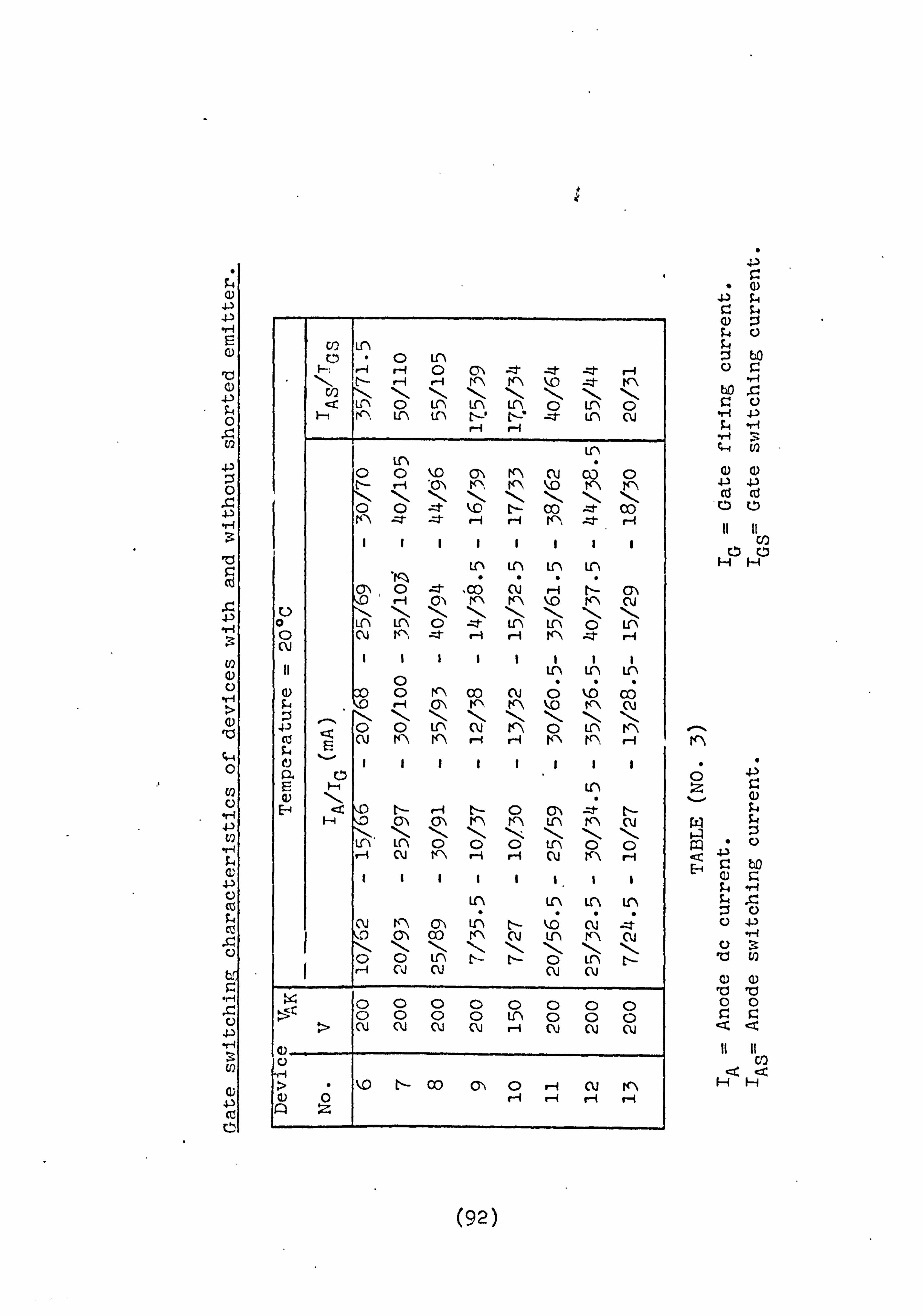
4.3
10 a)
4. ) $ý4 0
. Cý 02
4-3
4-3
Cd
S., 4-)
-r4 4-) to
4. ) C cz
CO Lr) C3 0 n
i-: r-I 0 CIN -: T -. t _:: I-
cr 0 Lr) n U-N o V) 0 rrý LrN Lo t-ý t---! -: 3- n C\j
r-i H
Ln 0 0 kD m n C\j co 0 I- T-i 'M KNI KIN %10 n "
0 0 -t 110 [-- co -I- co H r--l K-N. H
M, 0 4- lco Oj t- m H K'N C\j
0 0 --: t Lf) n C) Ln 0 C\j K'ý --t r-4 r-I K'\ --It r-q N
I I I I I I I I 11
0 Lý Uý Lý
a) ý 0 0 K'\ co C\j 0 %. D co ý4
: 21 .
,
0
1--, 4: ý <, K\
" t('\
-,, 110
-Z tr\
-,, N
--, 4--) 0 0 n N n LC\ n co H 94
V E-4 t-- C)
C31\ C\j LO Ln 0 0 0 n 0 C) f-4 CQ tC\ r-4 r-4 N
I I I U'\ Ln n
OJ rrN 0, \ Lr) t- ko C\j --zt I --,
M ,
CO --, K'N --,
N --,
Lr) --,,
" --,,
N -', 0 C Lr) tý- t-- o Ln L-- I r--l CIO N C\j (Xi
0 0
C) 0
0 0
0 0
0 n
0 o
o 0
o 0
ý> C\J N C\j N r-4 C\J (\) (\)
C. )
-H > ýo t- 00 0 r-, Cki n o) 0 r-I
Sý4
:5 bo
bD 'r. C. )
4-3 4. ) Cd Cc 0 (D
Cl) 0
E-4 r- bo
vv
(92)

10
0
.C U2
0
. r.
4-3
a;
Ic
F+- c
Er c
-rl
N 00 Lr, \ rý rrý ', D n L", co t-- NJ 'v
., c co o N L r I-i r-A n _: t r-I H n
p
-: t n C\j
Lf')
0 0 n K*ý KIN t- Lrl% C*li n Co t-- n N n N p
0 n N Oj CC) Lr'N N K'\ P-4 r-i r-A rAý r-I
0
co M H CU C\j %10 r-4 C) --t t- t- n Oj K'\ N CQ N, N-I ý1-1 1ý11 1-1 N" N 0 0 0 -zr 0 0 r-A K's H r-q F-4 rcN H
C13 ý4
0) E Qý - U'\ Ln E a) 0 t. - %, o co 'A r-i -: 4- E-4 ýý 4- t-- I'D t("\ C\j K') cQ
Nýl '1*11 N-1 Nýll N-1 ý1-1 11-1 0 0 n co co CQ Ln 00
H r-i (\j C\j r-i N
ko %. 0 Cý ON C\j H 00 --t t-- ko N r-4 K"ý 0i r-q N-1 INI, 1ý11 I--, "I-, CC) LrN 0 %lo %lo 0 0
Oj H N
-: t 00 -t t, - \, ý o oý \z :t ko %lo cu r--q rt r-i H N-1 **--, I-N N-ý, ---,
%. 0 0 n --: t -: 4- co L('\ r-4 r-4 r-i
ý4 C) 0 0 o 0 0 0
0 0 0 n Ln 0 0 n Ol N Cu r-i H 0i N r-A
CD 0
-, o tý- cc) 0-\ C) r-i r-I r-I r-4
v
0- 4.
E-4
S
4)
:: s bo
bo 1: ý 91
4. ) 4-) Cd Cd 00
co
Q)
c)
v (0
G) 0) 10 10 00 r. ' r.
9
(93)

4-)
10 0)
4-)
0
4-) :: s 0 c 4-)
10 $: I. cd
-H 5:
C)
10
q-4 0
ý5
0 cý \10 \Qo tr) r-I K-Iý C\j C\j CQ N" 'I-, I'll, llý *ýý '*-, < L-- 0 0 Ln rcl\ clý t-- --: t
F-4 H n -: t r-I H N n r-4
4)
H
z -ri
(T (1) Q
n
Cý n ol CQ V"\ C\J
N
clu t- Lr) CIN (3*\ rN Cý -4- %lo %-0 C\j r-i frN #--I
, -" --" -" --" --, I --" .:. t Lo Lr) C\j co 0i H (V n H H H r-I
I
Lr)
I I I I I I
ý, o co w 'i N co t kc) %, 0 (XJ r-I Ký C\j r-4 N-1 'I-, N" '*11 *1, --, ý1-1 N N 0 0 0 -4 n H C\j n r-i H H KN H
Ln N tý- L-- clý I-- xt \10 ý10 cu r-q C\j C\j H
N" Nl-ý Nlý Ný Ný N"
6 0 Ln CC) a) q C) CC) r-I oj 0i H K'*N
C) frý o Ln Lr) co Cý Lr. \ -f ko ko N . --I N r-i r-4
w Lr) 0 ý, D "o 0 0 ý, o H N N
co 0 co V-1% F-*ý ko t-- n R-ý Q5 p bi .. i N '1 -. 4 ý1-1 "1-, 1-1 **-ý **-, *-, ýý Ný-. %lo 0 n --4 - --+ 00 Vý -, Q-
r-4 ri H
0 0 0 0 0
I
0 0 0 Lrý U-\ 0 0 n CQ N CQ r-A H N N r-I
00 C3*N 0 r-i CIJ nI r--l H r-I H
0-1
rQ ct E--(
. 4)
6 (1) ;4 ;4
ý4 ý4 :1 bo
z
bo
Q) (D 4. ) 4-) Cd 0
0
it CQ
4ý Z:
C) 4-) . rA o. 19
'CJ u2
(L) 0) lö lö 00
(94)
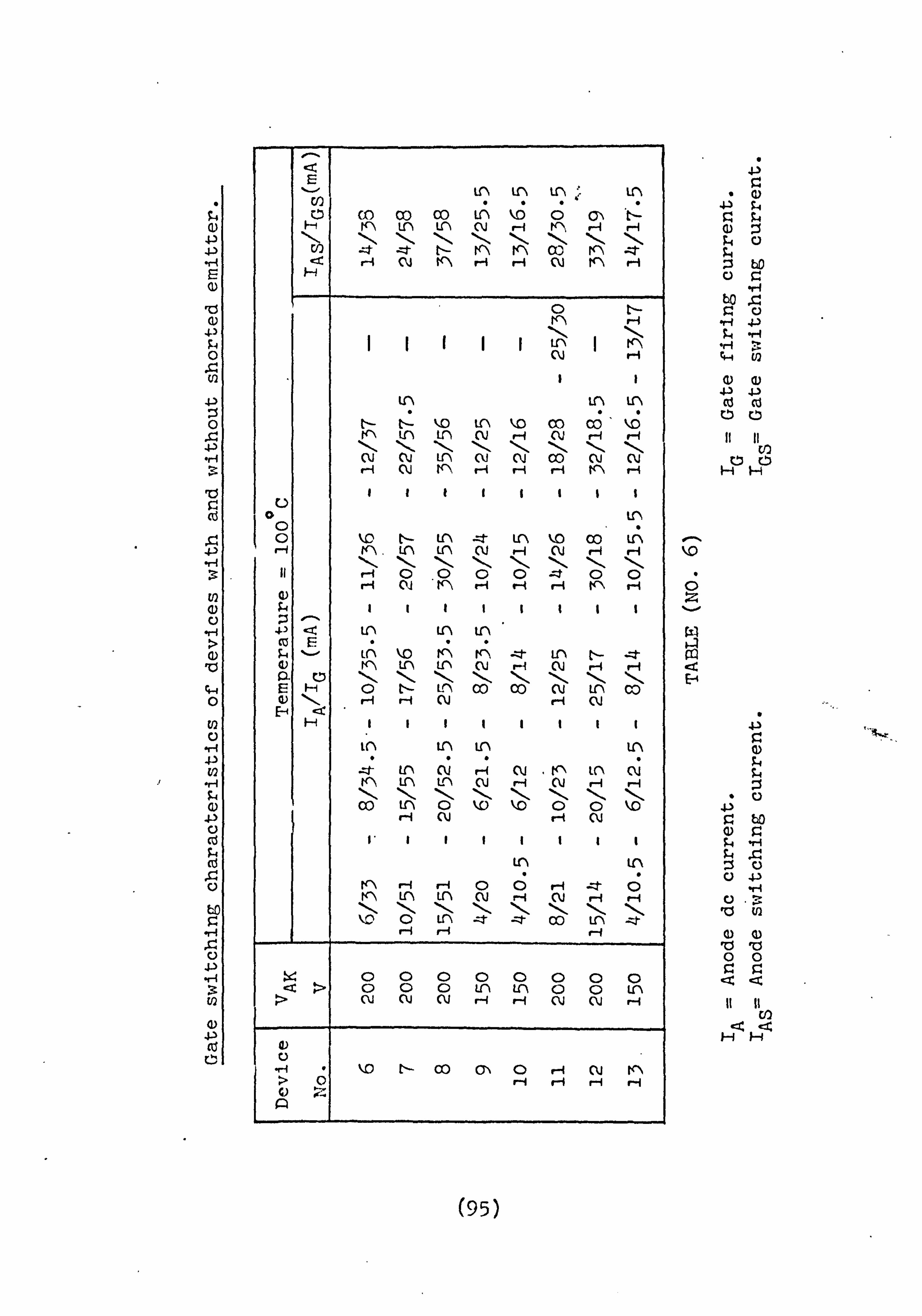
0) 4-. ) 9-4
0
Is:,. 4-3
Cd
v
r. --f 0
W 0
co $ý4
co
4-)
EQ
0) 4-3
Ln Ln n Ln C/) * 0 0 m co Co Lý ý, 8 0 o', t- F n Lr) V) C%j r-I K*ý r-I r-I 11-1 NN 1-1 Nýl "I-, N" CO -: t --t t- hlN n co n -4- H N K*N r-i r-4 CQ n r-4
C\j H
t-- t-ý "D n ý, o co Cý ký fýý Lr) LF) CV 4 Oj r-q H *ý-, '-, "IN,
:ý ý, N NN 1-1.
cu (Iti Lr, \ Oj C%j co Oj N r--l C\j K'\ r-i H H tr, \ r-4
0 0 kc t, - n -=r n "o co Lý
U-N Lr\ N 1-1 N r-I r-i
11 r-i 0 .0
0 0 0 0 H N Kl\ r-i 1--i r-i t('\ H
0)
4.3 CU F
Ln ko n K; -:: I- Lr) t-- -: t n Lr) Ln N r-I C\j r4 r-I 91 0 N-1 %*-, **-, %-, **-, 11-1 E ýý 0 El- Lrý co co C\j Lr) CO 4) Ný-, r-i H (\j N
Lr) Ul\ U"\ C\j r-( C\j t<'\ LO N
frý n V) C\j r-i C\j r-I r-q *1-1 ý1-1 ý*-, **11 N-1 CO Lr) 0 ý10 ko 0 0 ýo
r-I C\j V-4 C\j
Lr) UN C) 6
r-4 -t 6
n C\j H C\j r-j . -. I
ko 0 Lf'\ --* --: I- co n -: j- r-I r-4 H
0 0 0 0 0 0 0 0 cr ý> 0 C) C) n Ln 0 0 n
N N C\J
kD t-- co 01\ 0 (IQ KIN > 0 r-4 r-I H C)
(95)
0-%
110
0
. J)
:3 bD
bo 9
4-)
f4-4
4-3 co Cli 00
bD
4-3 -r4
a- : ý: to U2 a) Q)
10 TI 00 00
<
Cf)

Ic a 4-
c
Lf"% Ln Ln o
ci -t N H r-I INI NN NN --Zt- -* Ln r-I n ulý r-A H - n K'\ r-i n
c
ct
0-%
ce E
C)
I--, ct
NNH
n J"t N
Ln U-\ nn Lr)
LA Cý rN ý-: rCN --4- C\j H CQ ri H
C\j C\j N C\j co C\j r--i N KIN r-4 r-i H n. r--4
co 0 H00 J-4- C\j NHN r-4 r-i
H000000 r-A C\j t('\ r-I H r--l r('*ý H
Cý co --: I- oo Cý K; r-I N _-: I, -ti- NH r-4 T--l r-I I'll Ný. 11-1 *--, N., **-, "I-, N,
.0 t- Lf*N co Or) cQ n co H r-4 N r-i C\j
t, ý n cc) 60 Lr\ CQ -:: ý- -: T r-I CO r-i r-4
C', llýl N-, *-, *, --, 11-1 N" 11-1 co Lr) 0 ko ko 00 kD
V-4 C\j
Ln t- -t- (\i n ko ,0 cu -*- r-i ko r-i r-I Co *1-1 Nýll *ý-, l*N, N, N, N, N, ko 0 Ljr) zt -4- co n
r-i H O-A
000 Ln 0 VN HN C\j I-i
N-
E-4
V-1 . ko t- co Cý 0 r-i C\j IC\ ;> 0 r-i r-I H (U
p
. 1-)
94
bo rý C. )
-H 4. )
E/2
4-3 4-ý 0
4-3
bo r-:
C) 4-)
C)
10 V2
0) (1) 10 TI 00 0 I: i
(96)
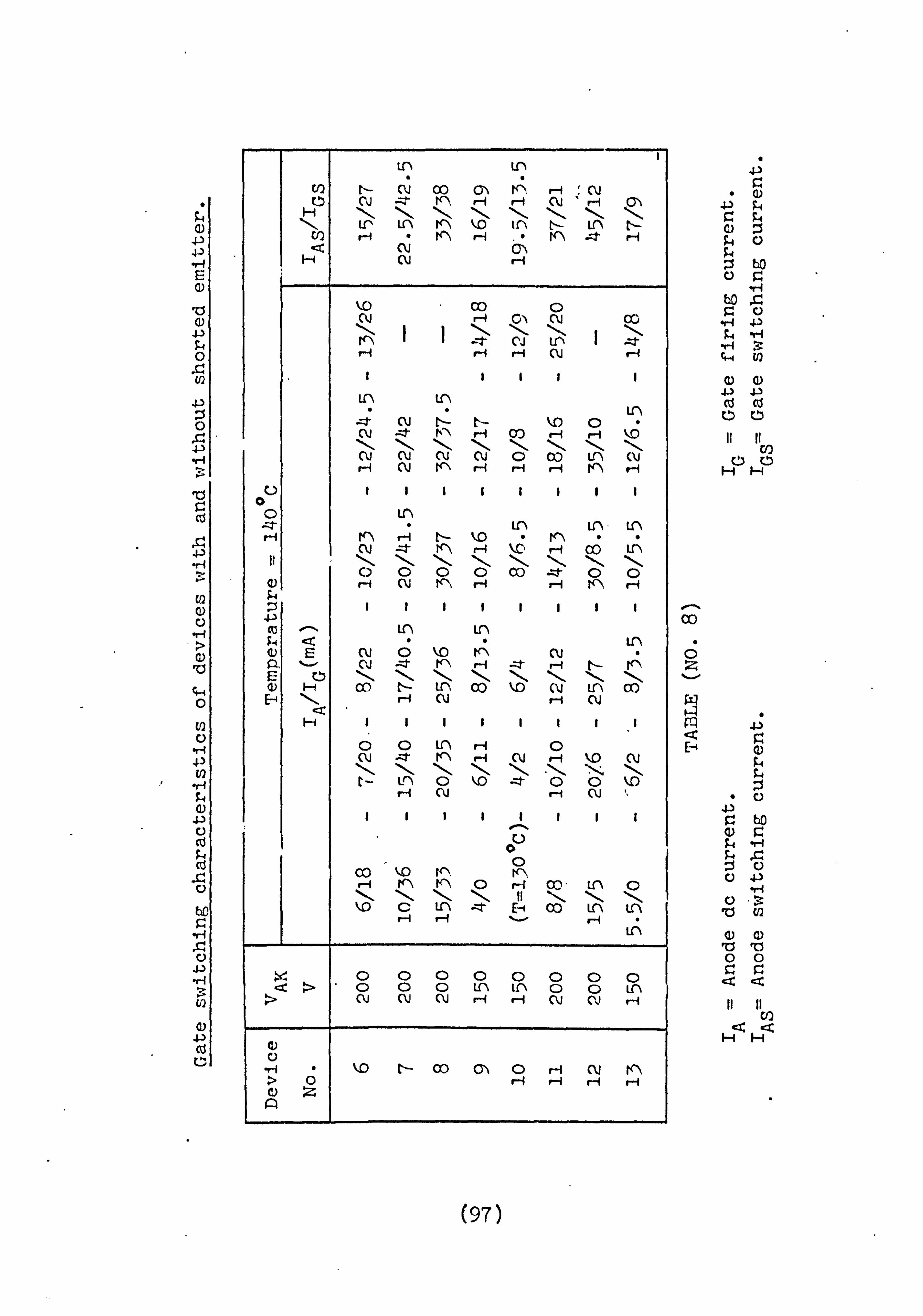
4-3 4-. )
4-3 P 0
. Cý U2
4-3
0 . rý 4-)
4-ý
CL
Ic
4ý
Ln Lr)
cr) t- Cý co CN Ký H f C\j H r-I
U'l U') %D tn tý- Lo r-A .0
Ký _: t C\j 01% N H
:Z
:: Z H
%lo co 0 N 22,
r-f HN r-I
Ln C\j 0
N 4- tc, \ HHH ko "N' Nýl ý11 %1-1 *1-1 *1-1 C\j C\j Oj N0 OD nN
N V-\
Ln Lf'\ Lr)
n r4 t-- %. 0 0n0 C\j =f ýQ
H \C H OD n N--l N-1 ýý 11-1 1%11 *111, C000 CC) --Zf 00 r-I Nn r-i H"H
(\I C; ko v; N U r-i 4-
CC) I- n co ko N Lr) CC) H C\j H (\j
00nH0 N 4- n r-i C\j r-I ýo C\j , *-, N, *, %-, "I-, '*-ý ý1-1 '1-, 11-11 t- Lr) 0 ý10 -4- 00 kc)
H 0i r-i (\)
0 co \10 VI\ K-N
K'\ 0 r-I Co -n0 **, -, **ý 11 INI INI lllý Lr) -: r OD Lf'\ Lf'\
x 0 (D 0 0 0 0 0 0 U'N c) (D n
Cu H r-i cm Cm r-i
Glý 0 r-1 cm tc, \
0. - CO
E-4
S
4)
z P4
;4
:: s bO
VA bo
94
q-4
a) (1) 4-1 4-3
CO
F4
bD
Q 43
00 r. ý::
CO
(97)

The Theory of Influence of Shorting Dots
in PNPN Devices.
The theory and applications of emitter-shorts for
improving the rate of rise of forward blocking voltage., lop20p2300
dV/dt performance have been discussed by several authors.
As we have seen one effective method of improving dV/dt
performance is to introduce a shorting resistance between
the emitter and underlying base.
Two attempts are made to derive the influence of shorting
dots, the first being the general case of resistance R,
placed between the cathode and gate which simulates a
shorting dot array. The second analyses current flow
in a direct manner without using the general thyristor
equations.
6.1 Resistance R between cathode and gate.
Experimental results showed that 'such a resistance
stabilises the operation of thyristor. Recalling equations
(1), (2), (3) and noting that IAý-Ill--, 21 IK =I -3
=I A +T G these
equations with assumption of [exp-/3V
2- 1] = -1 it follows
that:
,A[. exppvi
(78)
,A =Cý'<lN r"P IS1 [expp
V, -1 ]
+( r... l P Ps + Mn Ins) +'ý2N MnIS, 3
(98) '
[expp V3 - 1] (79)

--71-7-
C>< Isn +I exp pv
LJ (80)
Since there is an external shunt. resistance between
gate-cathode', figure (6-1), - then the forw ard bias of gate-
cathode will be
v3 sh R
but
I sh A+IG
V3=RIA+IG -0"<2I IS2 - 'S3 ( expPV3
- -,. Ish
K
A
Figure (6-1) pnpn with external shunt resistance R.
For small V3 we can write
i) tN.. * (exp v3 fiv
3 (Si)
therefore
v3- R(IA + IG - C5ý21 I. S2 - Is3PV3)
or
(99)
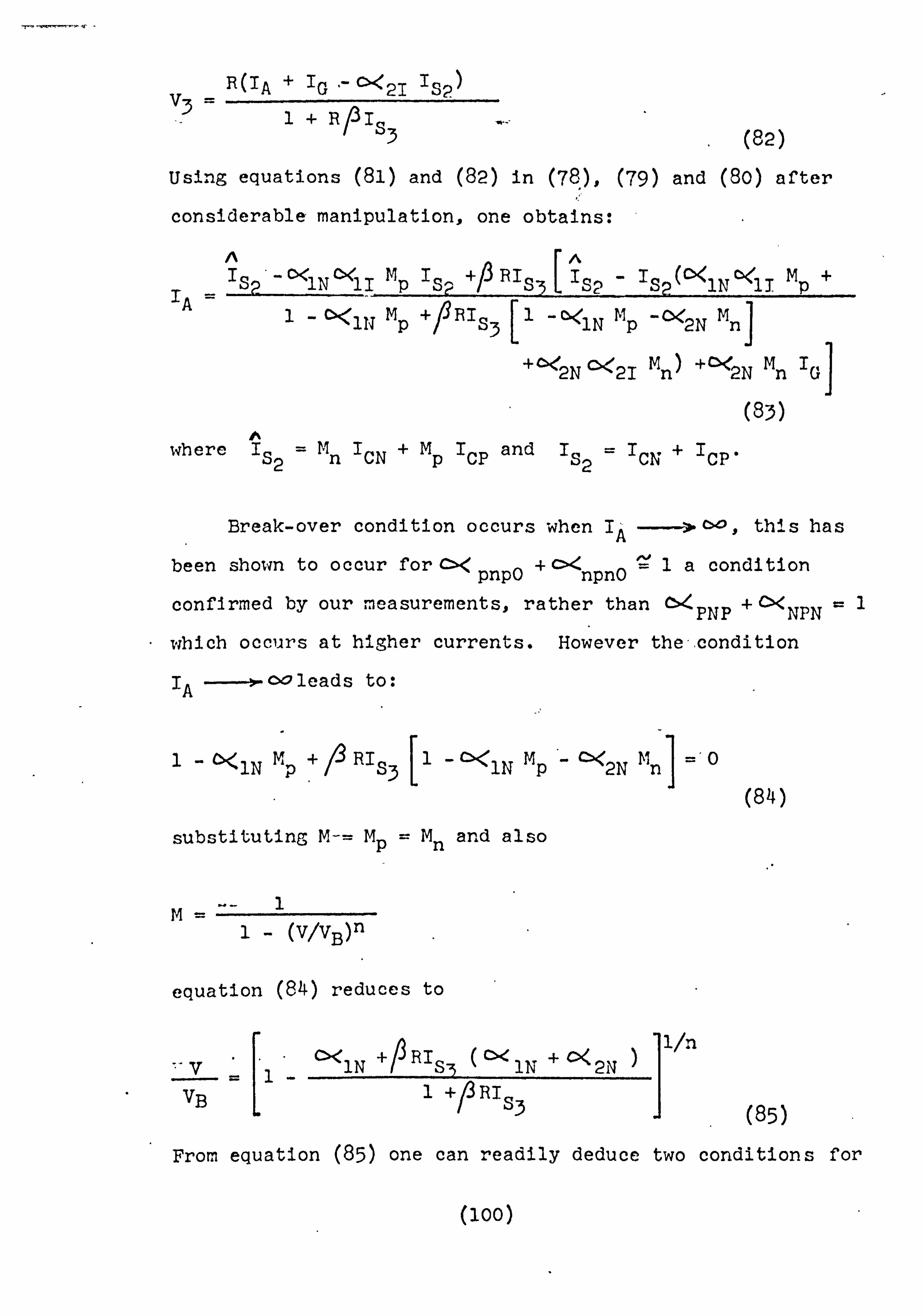
v3= R(IA + IG '- Cý'ý21 ISO
1+ Rpi S3 (82)
Using equations (81) and (82) in (78 1 ), (79) and (80) after
considerable manipulation, one obtains:
AA I C4 mII (cX
S2 0<1N 11 P S2 +P IýIS3 I
S2 - Is? 1N C'<l I 'A
1- (><'N MP +P IIIS3 [1- c'<lN Mp - 0<2N Mn
+
+4ý'ý2N Cý'ý21 Mn) +5< 2N Mn 'G
(83)
where I S2 =mnI CN +MpI CP and 1 192 =T CN +I CP*
Break-over condition occurs when I- >0-0, this has A
been shown to occur for (: >< pnpO + c>--, ' npnO*2ý
1a condition
confirmed by our measurementss rather than 0'4PNP + O< NPN
which occurs at higher currents. However the,, condition
!, -wleads to: A
1N Mp + //3RI i- c< 1N Mp *- Cý'<2N m nj =' 0 S3 (84)
substituting M, Mp= Mn and also
1- (V/VB
equation (84) reduces to
Cý< 1/n , -V 1N +PRIS, (C><
1N + CKI 2N
VB 1 +p RI S3 (85)
From equation (85) one can readily deduce two conditions for
1
(100)

0 and R 0-0 so:
V C', ) 1/n C>< 1N 2N VB
v 1. N
VB
B
R
Comparing these two terms shows that as R decreases the
breakover also decreases. though this is admittedly small
and agrees with experimental results.
Equation (83) could be simplified by substituting
MMp=Mn so that:
MI (1 C>< RI PII , I'
c: ><lNcý<lI + c><211C%ý2'I)l 'A
S2 lNc 11 S3 Sp
1-M 1N +PRI S3 [1 14 (, CN< 1N + 0. < 211)
+M 4>< 2N IG
(86)
1
re little avalanching occur- Well aiay from breakover , aheA
M=1. With R cpen circuited we can thcn obtain
S2(' -_"ý'<lNcý<'lT -C'<2NC'e2T) +Cý"<2N IG
1-C: "< 1N - ýý2N Isp
+ IG
1 (o< 111 + C<2N)
Since .+
With R=0 (86) becomes:
(87)
(101)

_ARO Cý< 1N Cý< 1N
Corr-paring equations (87), (88) it can readily be seen tbat:
AROO >
ARO
(89)
This has also shown by W. Fulop (private. communication).
Of great importance is the decrease in IA for decreacing
R. Another point of interest is that I ARO seems entirely
independent of 0< 2N or c-< 2V i. e, the transport properties of
an npn transistor. This can be lead to increased stability
of device.
6.2 Current flow with shorting dots.
Beforeinvestigating the influence of shorting dots we
shall look at the situation of currents without shorting
dots and gate open-circuited.
a* Without shorting dots.
--ion current I flows across a reversn biased The satural. coo I"
collector Junction as across any reverse biased junction.
If the inj . ected emitter current is I KI then by transistor
action c< NPN IK passes across to collector and (l -C, <IIPN)IK
"remains behind" (current due to recombination in the baseY
in the base of npn section, which is equal to I cOOn
(102)

disapparance from the base of npn, figure (6-2).
KG
cuuri lNrl\4' A
n cOOn
C><iIPN'K
cOOP PNP'A
p
flow of electrons
--a- flow of holes
+ IA I
Figure (6-2) PNPN structure with current flow under forward bias.
Yl- Cý'ýNPN) ý-- IcOOn
i. e.
r
II coon K
NPN (90)
Similarly, for pnp transistor with correspoding w<PNP and
,A. hence the collected current by collector of device Is:
,A= C>< PNP A+I COOP + C>< NPN IK+I cOOn
, A-* = icoo
c>< PNP - C><NPN (9')
Since A= IK when IG =0 and 'cOO ý2 IcOOn +I COOP.
Assuming the current contribution from the pnp side is
small, therfore
icoo ! L., I cOOn
(103)

b. With shorting dotS,
With a shorting dots the current across the device
will be:
cob C: )< PNP ff (92)
wherec-><eff is current-gain of np. n transistor modified
due to the shorting dot. Comparison with equation (91)
shows that only Cý'<NPN has replaced by Cý<eff' In order to
evaluate c><eff consider figure (6-3).
7K ?G
n K 1
DO E. F. in base proportional to applied
Ip
JL
voltage bias ------ causing I 71 - C><
L
F qo , NPN n4!
n Y' TDO flow of electrons
0< -I CO C"<NPN'K
= pNp A 01< I ne
NPN c()/l- NPN
__j flow of holes,
p
+6A
Figure (6-3) P14T PN structure with shorted emitter with
current fýow under forward bias.
Ico = (1-AS)IcOO is the saturation current across the
.LL Lo collector ýunctior- of the np-"i sectlon facing unshorted
- emitter. , DO 2ý AS ICCO is the saturation current flowing across
collector of npn opposite shorting dot.
(104)

ICOO ý-- the total saturation current across the Alace of
collector junction and AS is the ratio of shorting dot
area to total emitterarea.
The emitter forward bias voltage will as. -Jume values
schematically indicated by the dotted line in figure
This will cause a built-in electric field in the quasi-
neutral p-base resulting in a leakage current IL flowing
as majority carrier hole current out of the shorting dot.
This hole current I J6* I LI must be compensated by an electron
(particle ) current out of the emitter. If this additional
emitter electron is I t1henc>< ,, "I passes to the collector n NPIT n
and (1 -c>< NPN)In remains behind in the npn base.
Therefore rI
NPOIn " 1L
(93)
-hat the If vie assume that all I's are positive and
currents into- the transistor are positive, then:
IEN (1 -A S)Icoo IL -ý AsI
coo 1 --c><NP'N'
'CN = (1 - AS)ICOO c< NPN(l -- Aq) Icoo
1- Cl< NPN
(94)
O'<NPN In + A'S Icoo
(95)
Since 'r +10 for 10 the equation (93) follows. ýEN CN G
Substituting: ) equation (93) into (95). gives:
ICIT -
lcoo (1 - AS) Lc: '. <NPN
+AsI coo 1- r->< NPN - C-ý NPN
(105)

or: ICN coo
NPN (A
s+ Cý$<NPN I
)Coo (96)
Comparing this equation with equation (90),, i. e.
I coo iON one can clearly see the influence of AS
and 1L in reducing the current, therefore reducing the
total current A*
Thus the effective alpha can be defined as;
Cl< c>< (AS +
or:
ef f cý'ýNPN NPN I coo
Cx, NPN
[1- (AS + It00
eff -cý<NPN(AS +I
IL
coo
This clearly shows that:
(97)
Cý< ---A- C>< when A0 then 1 0, this is of eff NPIT SL
course the case without shorting dot..
C: -< 0 if A1 then again I -o- 0, in this eff L
casee the npn transistor tends to operate as a "pn" diode only.
Substituting equation (97) into (92) yields:
A Cý'< PNP - C<Illpil
icoo
1- (A .s+
ILIIC
.
COL,
1- C>< NPN
(A S. + ILIICOO)
(98)
(106)
Equation (98) shows the effect of AS and IL in reducing
the current which gives qualitatively-good agreement with
the previous analysis where R bet -ween gate and cathode
reduced anode current, that-is
IAR oO I>I IAR 01
6.3 Evaluation of IL (Lateral-hole current).
We earlier said that the rate of electron left behind
in the p-base of npn transistor section is equal to the
saturation current i. e.
rate of electrons "left behind" =I coo
This shows that where VE(x)-= VEOO the maximum value of
emitter forward bias there is a perfect balance of the
one dimensional ("vertical") current flow. For the device
with shorting dot we can assume a distribution for emitter
forward bias as shown in figure (6-3); this is indeed the
case when VEW = VEO only at the point x=O. At any other
point x the rate of electrons le. ft behind is smaller IV -han
at point x=O, because as one moves towards shorting dot
from x=O, the emitter forward bias decreases. Hence the
electrons injected by the emitter will be less than the
case for maximum Vj,: (x), and thus the rate of electrons
"left behind" will be decreased.
(107)

Assuming ICOO flows at uniform density, then some
electrons must be created in order to compens,, jtQ the lower
rate of electrons "left behind". These elect-ron-hole pairs
will be generated by 11generation-recombination" in. the
p-base, thus the excess holes must be flow out of the base
through a shorting dot, in order to keep charge neutrality
in the base. These holes will constitute the leakage
current IL out of the base, therefore:
d'L =II�ý001 -
li, (X)1(1 -CK i dx NPN) +i Ale><PNP
(99)
where IcOO ý IcOOn +I coop"
The injected emitter current I. can be expressed in
the usual way as Ebers and Moll (1954) as a function of
emitter-base voltage VE (x):
JE (X) C, <
i EO
O<
Ie qv E
(x)AT + CI< NPNJ
NPN INPN (100)
where JEO and IcOOn(current/area) are positive quantities.
en, unit 1 gth
mmmý K
--
--. n
VEO unit length -L to
paper.
v AOO
A
Figure (6-3) Schematic pnpn model under consideration.
(108)

Assuming a distribution for anode-forward bias (J 1
junction) as shown in figure (6-3), the current*J A will be:
JA 1- icoop
11 Cý'<PNP
(101)
substituting equation (100) and (101) into (99), after
manipulation, one obtains:
dIL icoop +I
JEO (I C: ý'ýNPN) e
qVE (x)/kT 1+
dx PNP cOOn C>< NPN c: ><INPN
+ CK NPN
Now letting
2
A coop +I+ JEO(l - Cý"4NPIT)
0. < PNP cOOn CN< NPN Cý<INPN
B JEO(l - 0'<NPN)
1- cý<NPN Cýý'<INPN (102)
we will have:
dl L=AB exp qV E (x)/kT
dx (103)
The current I L(x) causes a voltage drop given by
_dV ('3
1 L-(X) dx W (104)
where 'P is a linear resistance of the base in the x VI direction and !. -I is the width of p-base. Differentiating C5 equation (103) with respect to x and substituting one gets:
(109)

-d21L qB exp
qVE (x)
- dv
dx2 kT kT dx
=-q (dIL _ A). p1L
(x) *, kT dx w
d21L+*I dI L qAp _I 0
dX2 kn-I L. dx kTW L (105)
It is convenient to make the equation (105) non-dimensional,
therefore noting that IL is current/length, we will assume:
y IL(X),
kT
qf x Z -T
and
dI L kT dv dx dz
d2 IL kT d2y dX2 qpl, 12 dZ2
I L(x) = kT qp
x=z"W
clubstituting the appropriate terms into equation (105) yields: ,j
_d 2y+y dv
- -A-Y =0 dZ2 dz kT
and asbuting CA kT
dy+y --ý-y - CY =0 dZ2 dz
we will get
(106) (110)
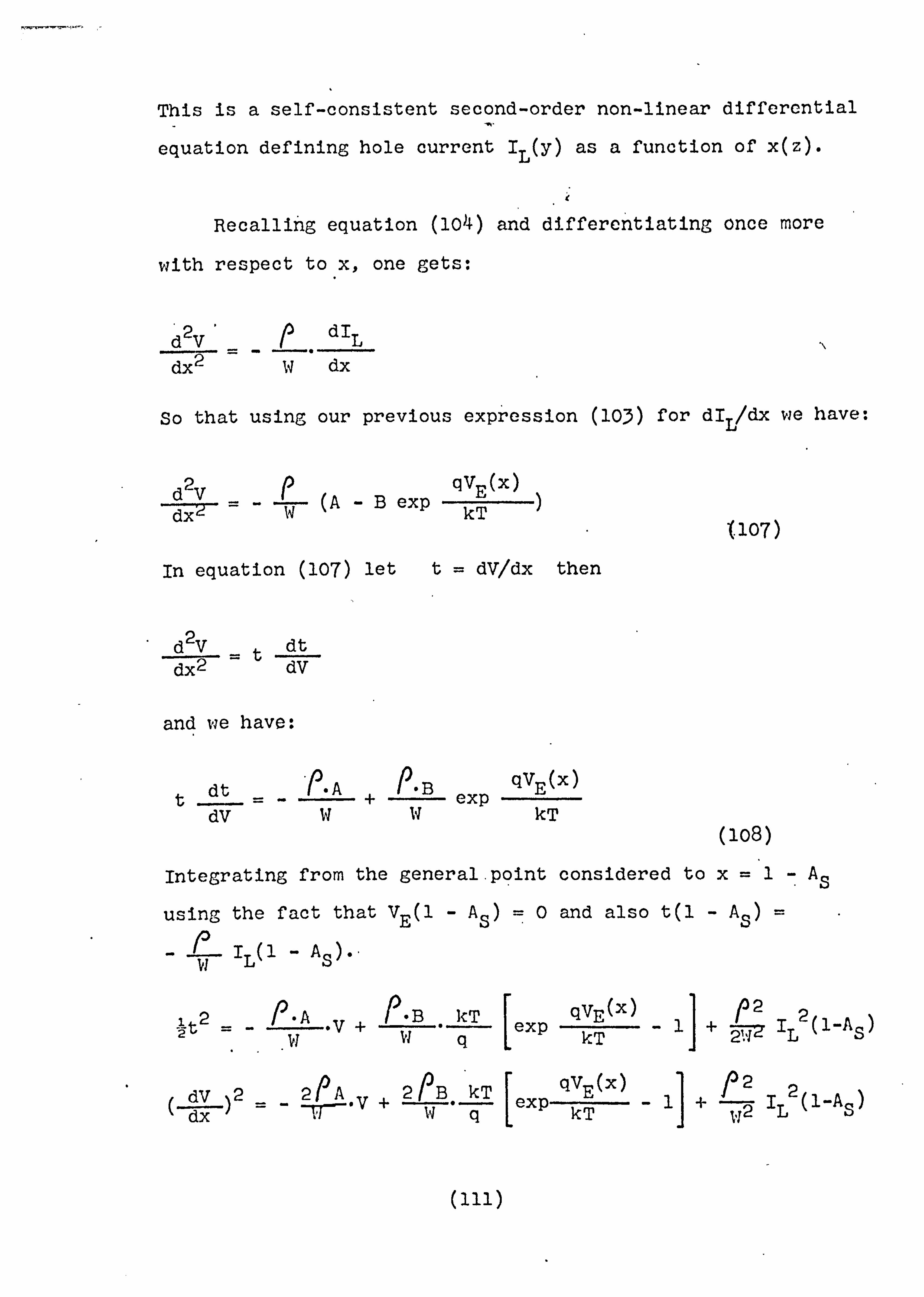
This is a self-consistent second-order non-linear differential
equation defining hole current I L(7 ) as a function of x(z).
Recalling equation (lo4) and differentiating once more
with respect to x, one gets:
d2v dI L dX2 dx
\
So that using our previous expression (103) for dIL/dx we have:
d2V (A -B exp qV E(x)
dx2 W kT M7)
In equation (107) let t= dV/dx then
d2vt dt dý2 dV
and vie have:
t dt P,
A 4- exp
qVE(x)
dV ww kT (108)
Integrating from the general-point considered to xA S
usin, fr, the fact that VE(l - AS) 0 and also t(l - AS)
- /0
1- AS). - V1 L(l
it2 =_ /)-A
V+ .- ICT
exp qVE, (X)
_1+ P2
12 (1-AS) wwq kT =211 L
dV )2 2PA. 'kT qv E
(X) p22
dx 77- v+W, q
exp kT + 1,12
1L (1-AS)
(111)

Assuming
2PA w
and M= _2PB . kT
1.1 q
qV E (x) 1
dV_ =±
[M(exp 1) - D-V +
e2 , 2( 1-AS)
dx kT W2 L
xp qVE (x) /D2 2
n
[M (e
kT D-V +14 (1-AS) +
fo dx
0 (109)
and using the boundary condition VE (X) = VEO and also
dVdx =0 at x=0, this is the complete solution in terms
of an integral.
Computer Aided Solution of Equation (106).
The computer aided method of "Digital-Analogue Simulation"
is used to solve the non-linear equation. 'Program uses the
Merson's modification of the Runge-Kutta integration formula.
This is a fourth order method which, can be made numerically
stable by choosing a sufficient number of step-lengths and
it permits reasonable economy of processing time by regulation
of step-length according to integration error involved.
The process uses the following equations (L. Fox, 1962).
yY+ -1 (K + 4K +K n+l ýn214.5)
where y* is the known value of Y at time t* nn
y n+1
is the value obtained for Y at time t n+Ij.. = tn +h
Kh' Y(tn' Yn)
(112)

K21h .3
K3 113 h
K4 113 h
K5 1/ 3h
I Y( tn+ 113 h, Yn+Kl)
+ h, Y+ lK +K Y (tn 113 n ýý 12
f1 Y(tn+ ; ff h, Yn+3/8KI+ ? /8 K3
Y(trý-h, Yn+3/2 K, - 9/2 K3+ 6K4)
in which h time step =t n-l -tn .F Y(t, a) is the value of Y'at solution time t,
assurning that Y(t) = a. I
The above formula specify the calculation of values for Y
and the K's, given values for Y"at each value of time.
At each attempt. step carried out according to the above
formula, the Merson truncation error formula is evaluated
for each integration output;
ey =ý1 (Kl - 9/2 K3+ 4K 4- JK 5Ry 5)
where Ry is a normalising parameter whose value depends
on the error checking mode.
Figure (6-11) represents a block-diagram of the Program, C)
used in terms of simple integrators, as is required in
programming analogue computers. To represent figure
at the point "P" we may write:
y ff
=, -ýy 0+ Cy
y to + yy ,- Cy =0
(113)

cy.
Figure (6-4) Simple block-diagram, of program used.
The program is adopted to use the computer library
manuals, D. E. Hirst, on CDC 7600 machine. The calculation
takes about few seconds (4 see. ) on the CDC 7600.
Boundary Condition.
Recal; ing equation (99)
dI L icoop +I cOOn i E(x)
1 (1 - cý'ýNPN) +I JAI C>< PNP dx
we can say that at the. point x. = 0 we have perfect balance
between the rate of electron "left behind" in the base of
npn and collector'saturation current, that is:
, coon. ýIi E(x)l (1 - c< NPN)
Thus at this point with a good approximation we will have:
(ilk)

dI I
dx L=I
cOOp + IJA Cl< PNP .. Coop 11- 0"" PNP
(110)
Also at this. point- the value of 1 0, i. e. L
IL =0 at x=0 (111)
Hence with such an initial boundary condition and
known parameters after calculating the constant C, we
numerically solve the second-order non-linear differential
equation of (106).
Figure (6-5) shows the variation of y(I L) as a function
of z(x) for various AS at constant 14 for the non-linear
equation of (106). This shows that as AS increases y(I L)
decreases at the point (1--- AS); this is expected since
an increase in AS for a fixed total emitter length will
decrease týe emitter junction area, and thus injected emitter
electrons. Variation of iL as a function of AS at constant
W is also shown in figure (6-6). The effect of AS seems
to be more pronounced than W at higher As in reducing the
hole current IL at the point (I - AS).
Figure (6-7) illustrates the variation of y(I L) with
z(x) at constant AS for set of different W. Of interest
here is that the slope of curve increases with increasing
W. The variation of IL the hole current with respect to W
is also shov. 1n in figure (6-8); this shows rapid increase
for IL as W becomes smaller. However the variation of
(115)

L (1 - AS) with AS and W is ta
- bulated in table
IL (1 - AS), jpA/cm,
A3 3 W01m) 0.0375 0.0675 0.125 0.20
15 84.3 8o. 6 75 68.1
20 82.5 78.7 73.7 66.8
30 8o. o 77.5 72.5 65.6
Ito 78.7 76. p 71.8 65.4
50 78.0 75.6 71.2 65.2
Table
(116)

Calculation of the Voltage Across the
Junctions in the "OFF" Parts of the
Thyristor Just After Turn-on.
One of the theoretical problems in the operation of
thyristors is the voltage distribution in the two central I base regions just after the device has switched on but
before the plasma has had time to spread. With the overall
voltage of the device having Oollapsed and the centre
- ched - junction heavily forward biased in a very small swit
on region but baing either reverse or at least not heavily
forward biased over most of the device, this must lead to
a very uneven voltage and field distribution in the two
, base regions. This could surely have a strong influence
on the plasma spread as well as on the flow of majority
carriers required as capacitive currents for charging up
the central junction into forward bias in regions still
switched-off.
The corresponding energy-band diagrams for the
-ate Are equilibrium, forward OFF state, and forward ON st
shown in figure ( 7-1a), (b), and (c) respectively. In
equilibrium there. is at each junction a depletion region
with a built-in potential which is determined by the
impuritly doptn(u; profile. When a positive voltage is
applied . to the anode, junc. tion J2 will be reversed biasedp
while J, and J3 will be forward-biased.
(117)

G
JP J3
A K
(a) Equilibrium
(b)
f
T v OFF
Forward "OFF"
VON Forward "ON"
Figure (7-1) Energy band digrams of forward regions.
7.1 The Rubber Membrane Model.
In order to-visualize the distribution of voltage
in Junctions, the rubber membrane is used. The rubber
membrane used was of unstret-ched thickness 0.048 cm. and
had a 15,55 stretch on a rectangular frame, the dimensions
of which were large compared with the "electrode system". 01
Figure (7-2) shows the frame with stretched rubber
membrane and electrodes.
(118)

The rubber membrane was divided into two parts, one
shOW4L. ng the potential distribution of the thyristor in the
"ON" part of the dev4Ace and second part showing the "OFF"
part of the'device just'. before plasma has had time-to
spread. In the "OFF" part of the device due to the presence
of the cathode metallization, tho voltage drop will be the
same value as "ON" part, i. e. VON* The potential distribution
just after the device switched "ON" in "OFF" part J. s shown
in figure
J2
np
cathode Anode
IQ "Equilibrium
VON ------ V C VEB
to "0/I. V PIV
-ON
4ý /, ,,
"OFF" region
Figure (7-3) Potential di. stribution just after turn-on
but before spreading.
(119)


What happens here is, the hole and electron displace-
ment current (I Di sp
1 Disn is discharging the V BO junntion
and reverse biasing the PIV (Anode junction) and cathode
junction "EB".
The maximum reverse voltage the cathode junction V EB'
can carry is probably less than 1OV. This is because this
junction has a very low breakdown voltage. So after the
breakdown of the cathode junction the majority carriers
will flow into the centre junction in order to reduce the
reverse bias of the junction, and finally the junctions J1
and J2 will share the reverse voltage in the manner as
, shown in figure (7-4), which demonstrates the potential
distribution at final'stage after all events.
J3 J2
I VON
T cathod
Figure (7-4) Distribution of potentials after settle-
down of junctions. 0
(120)
0
)de
e

Assuming that in the "OFF" portion of the thyristor
the total voltages across the junction have remained at
V0 FIII -1 then:
VOFF "": VEB + VC + VPIV
(112)
but the total voltage drop when all three junctions are
reversed hiased is:
vvvv ON c PIV EB
(113) Sub trac IV -ing equation (113) from (112) one obtains:
-v= 2Vp, V + 2VF VOFF ON B
therefore
.! (V v Piv 2 OFF -v ON) -v EB
(114
and also adding equation (112 ) to (113 ) will give:
v OFF +v ON ý-- 2v c
or V= .1 (V +V c2 OFF ON)
(115 ) is very large then: if VOFF
vc =-v PIV
(11 (121)

7.2 Computer Simulation.
The exact numerical modelling approach recently has
proved to bb an efficient means of solving the general
semiconductor transport equations accurately without the
conventional restrictions such as locally neutral or
space charge regions, constant mobilities., simplified
doping profile, etc. T1.1-Is approch, involving the solution
of the governing differential equation, was developed and
applied for the , L". 'Arst time Idy Gummel (1964).
Gum. mel described an efficient method for solving
one-dimensional (1D) steady-state carrier transport equations.
'Later many authers published solution methods not only
for small-signal and transient operation on 1D diode and
transistor structures. With these method s it is possible
to study bow physical parameters such as doping profile,
carrier mobilities, lifetimes, and gecmelkry are related to
the electrical behaviour of the device and t --o get a clear
insight into high-level effects that are of growing import-
ance for device optimization and design of accurate circuit
models.
However, the basic equations governing the transport Cl
of carriers in semiconductor structurs are Poisson's
equation, continuity equations for holes and electrons and
current density equatlions.
(122)
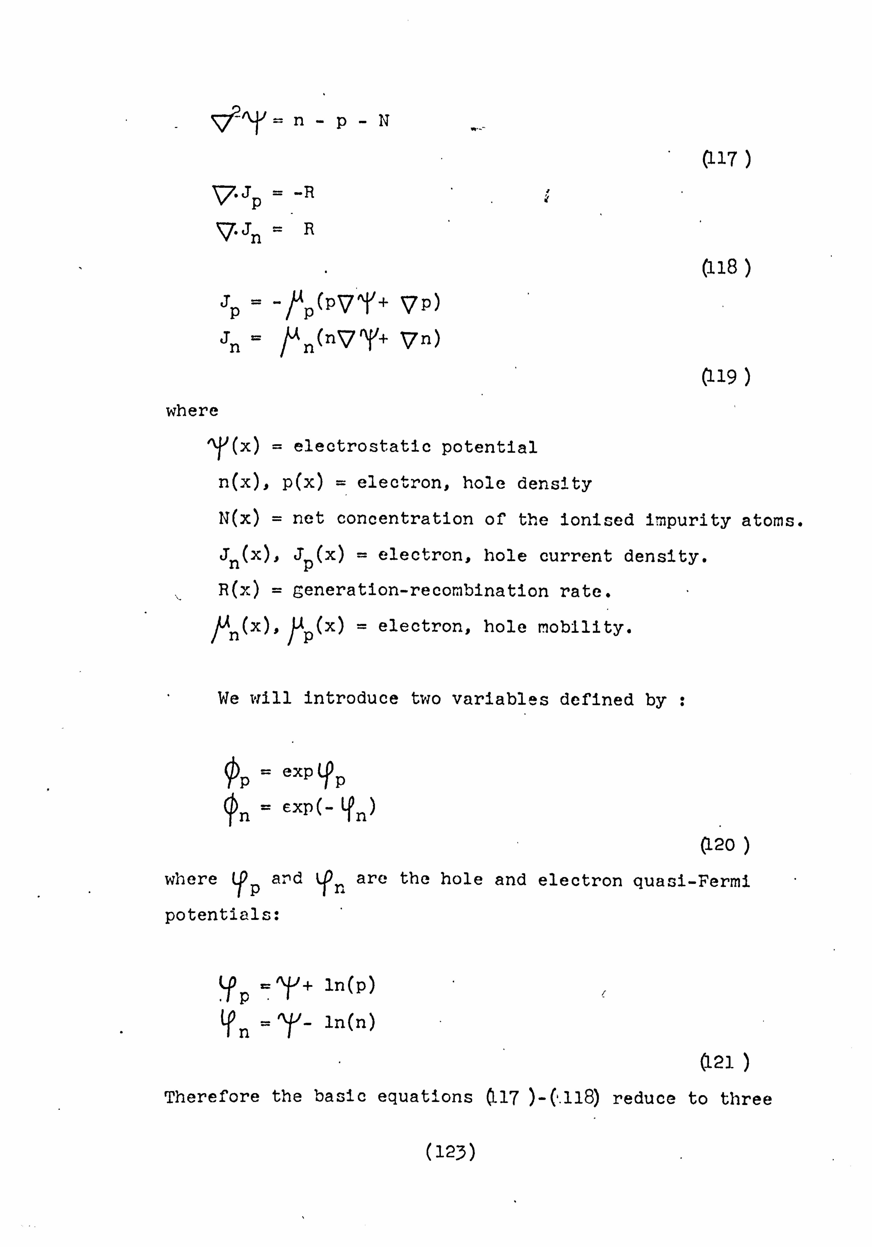
V-Ar
=
(117)
7. Jp = -R
V. Jn =R
1
(118) ip= -ýP
(PvAf+ VP)
Jn = Pn (nV Y+ Vn)
(119)
where
Y(x) = electrostatic potential
n(x), p(x) electron, hole density
N(x) = net concentration of the ionised impurity atoms.
in (X), Jp (x) = electron, hole current density.
R(x) = generation-recombination rate.
n(x), Pp(x) = electron, hole mobility.
We will introduce two variables defined by :
OP = exp yp
ýn = CXP(- Yn)
(120 )
where TP ar d Tn are the hole and electron quasi-Fermi
potentials:
yp 7Y+ in(p) Yn : ý* Y- in(n)
I
Therefore the basic equations ý17 )-(. 118) reduce to three
(123)
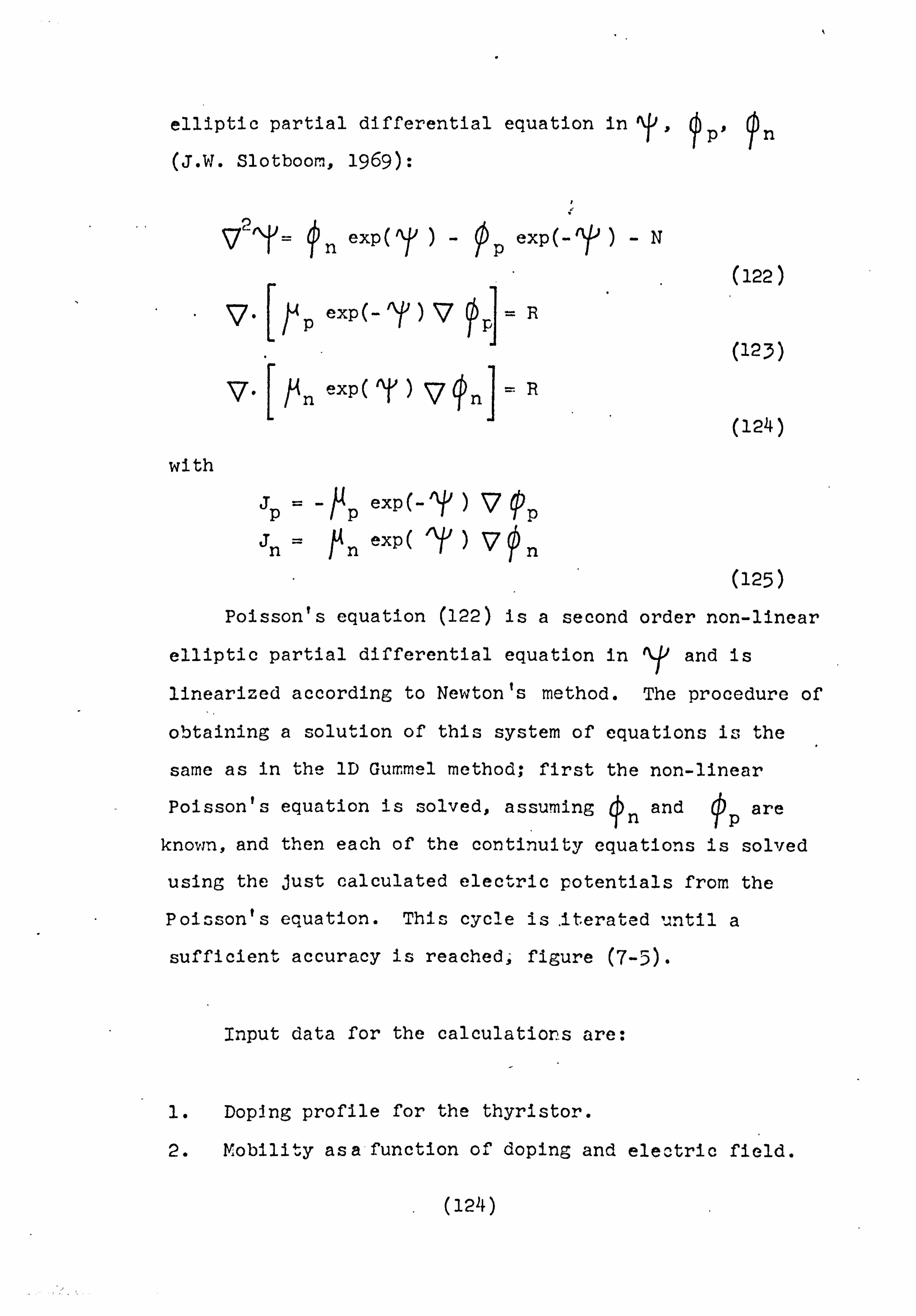
elliptic partial differential equation in ýp n
(J. W. Slotboom, 1969):
v2 fy= ýn exp(y
Op exp( N
(122) [pp
exp(-'Y) vý PI ý2 R
(12.3)
V' exp(y) Výn] =R
(124)
wi th
Jp=- Pp exp(- V pp
Jn 22 Pn exp (Výn
(125)
Poisson's equation (122) is a second order non-linear
elliptic partial differential equation in y and is
linearized according to Newton's method. The procedure of
obtaining a solution of this system of equations is the
same as in the 1D Gumme-1 method; first the non-linear
Poisson's equation is solved, assuming ýn and ýp
are
known, and then each of the continuity equations is solved
using the just calculated electric potentials from the
Poisson's equation. This cycle is Iteralt; ed until a
sufficient accuracy is reached, figure (7-5).
Input data for the calculations are:
1. DopJng profile for th-e thyristor.
2. Mobility asa function of doping and electric field.
(1211)

3- Carrier Zeneration-recombination law. 4. Applied voltage. 5. Geometry.
6. Right boundary condition.
begin
Guess ýns ýp and R, Yn, Jlp
solve Poisson's equation
solve equation (123) linear in (P-
solve equation (124) linear I in 0,,, . --'Test '
accuracy reac 'ý'ýe
s
end
Figure (7-5) Flow chart of the iterative scheme.
Doping Profile.
The doping profile is calculathd from the 1D Gaussian
diffusion equation:
(125)

N=N exp (X, -Re) 2 /(eK )2 N exp(-X
2 /(bK) 2)+N 223+ 114
(126)
where: 411
N, = c>urface density donors, concentration.
N2= surface density acceptors,. concentrati on.
N3 epitaxial layer concentration.
N4 fourth layer concentration.
eK diffusion constants, donors.
bK = diffusion constants, acceptcrs.
Re = flat top.
Mobility Model.
The carrier mobility variation with doping and
electric field have been presented for silicon by D. M.
Caughey and R. E. Thomas (1967).:
Pmin_ +1+ (E/Ec)
w ýmiln I
1+ (NINref) (127)
where P is mobility and N is doping density. P is
constant, and equal to unity for holes and two for electrons.
The value ofChýand N ref can be obtained from the slope
and. unity intercept of the straight line of;
109( P max -P )I(p -P min) versus log N.
ae W"red Pmax -P)I(P- Pmin)
(126)

Recombination Model.
The rate of recombination for ngn-equilibrium but
steady-state condition is obtained from the Hall-Shockley,
and Read model:
R= (pn --n )2/ [Cno(P
+ Pl) + -Cpo(n + nl)
where
_Cno' 'Cpo = electron and hole lifetimes.
pl, n, hole and electron concentrations that
would exist if the Fermi-levels were at the trap
level.
For simPlicity we will assume that the recombination
centres are near the bandgap so:
n, = p,
therefore
e. 'fp - Tn
1
0 (e
Tp -nf + 1) + 'Upo(e
Aý- Tn
n (128)
Note that, p and n are in units of nip the intrinsic
carrier concentration, and y .0
Ipp and Ifn are in units
of the Bolzmann voltage kT/q.
Boundary conditions.
For the discussion of the boundary conditions we will
(127)

treat a tIrlyristor as a "hook transistor" as shown lin
figure (7-6). it
IN B
pc
1 In In
np+N ep p 1 %'
1 en
k3
L--- VEB- -- -j --V -ý» ____j CB-'
Figure (7-5) Schematllc of npnp hook-transistor under
corsideration.
Boundary conditions are specified at points
representing the emitter, base and collector contacts.
Along the contacts infinite surface recombination velocities
are assumed,, or in other words, the carriers are assumed
to be in thermodynamic equilibrium. Also it is assumed
that the charge neutrality ccnd"Ltion is valid along the
contacts. Therefore the carrier densities at the emitter
and collector are fixed.
pn =1
n-p-N=O
(129)
It is convenient to talte the base as refference point
for the electrostatic potential. The potentials at Ithe
emitter and collector are then determined from the diffusion
and applied potentials. In practice the approximation is
(128)
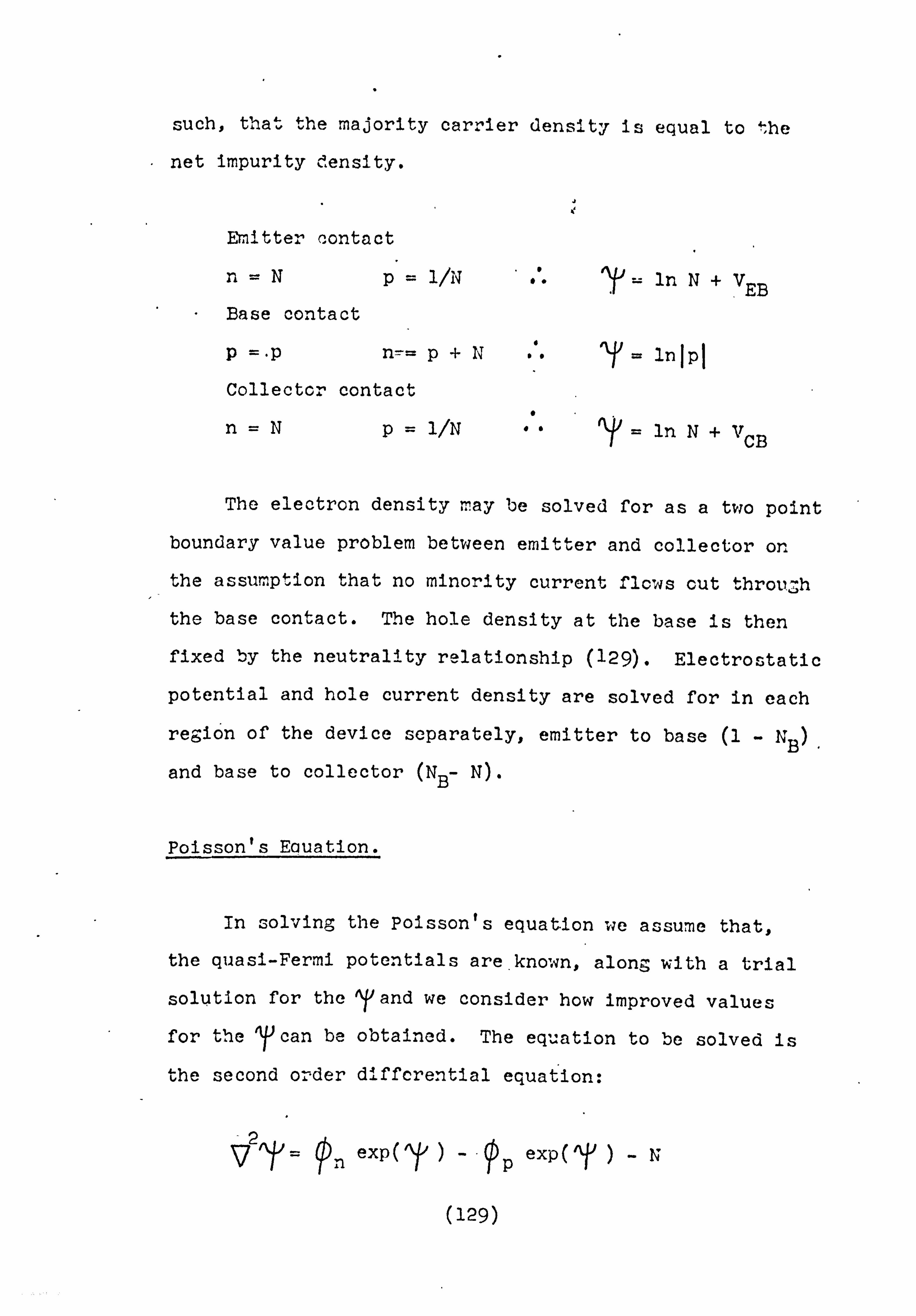
such, that - the majority carrier density is equal to the
net impurity C-lensity.
Emitter contact
n=Np 11N
- Base contact
p =. p n- p
Collectc. -, contact
11N
ln N+ Vn.,
040 y= inipl
ln N+V CB
The electron density may be solved for as a two point
boundary value problem between emitter and collector on
the assumpt -ion that no minority current flows out throuzh
the base contact. The hole density at the base is then
fixed by the neutrality relationship (129). Electrostatic
potential and hole current density are solved for in each
region of the device separately, emitter to base (1 -N B).
and base to collector (N B- N).
Poisson's Eauation.
In solving the Poisson's equation we assume that,,
the quasi-Fermi potentials are. known, along with a trial
solption for the Y and we consider how improved values
for the Y can be obtained. The equation to be solved is
the second order d. Alffcrential equation:
-2 V Y= ýn exp(y ýp exp(y N
(129)
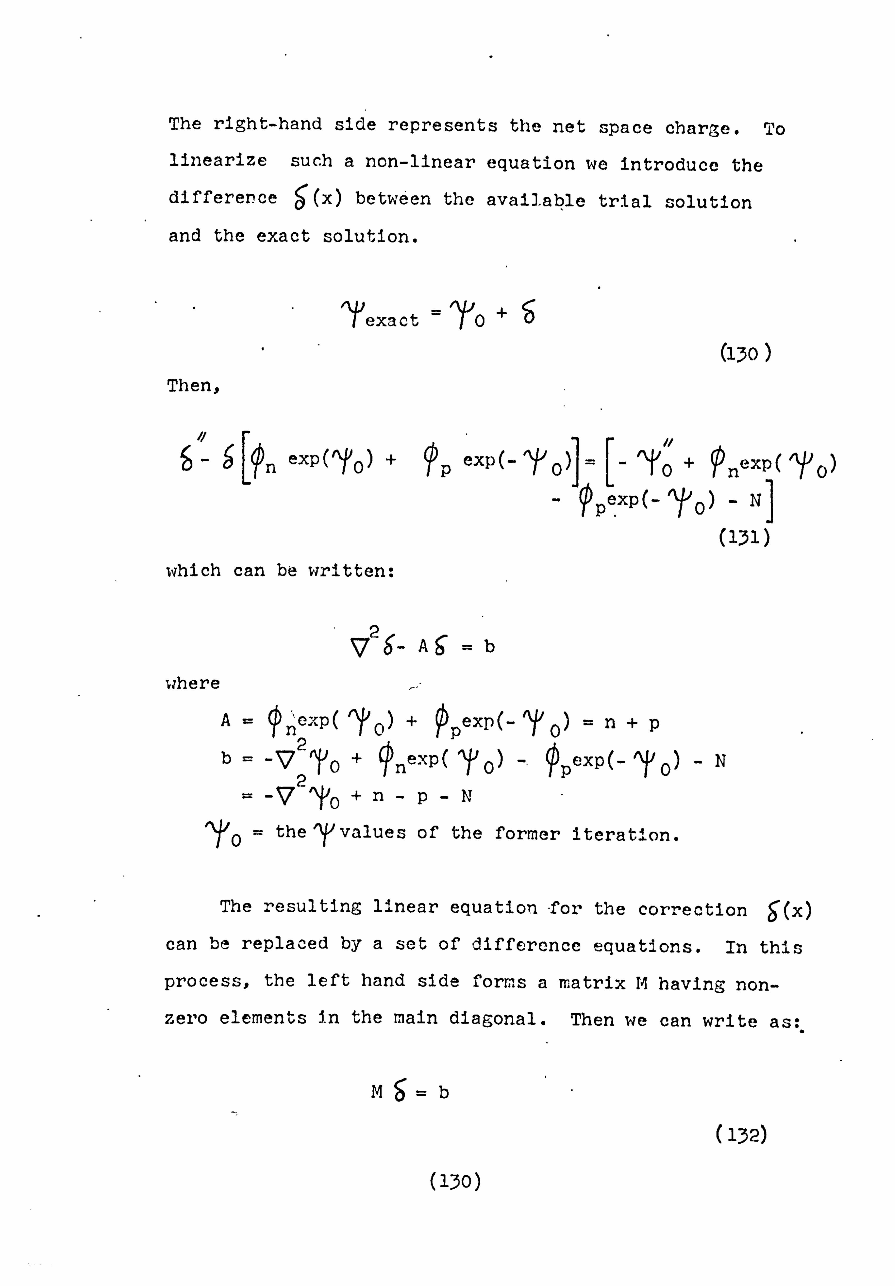
The right-hand side represents the net space charge. To
linearize such a non-linear equation we introduce the
difference g(x) between the availaýle trial solution
and the exact solution.
Yexact = To
(130) Then.,
9 [ýn
exp (? 0)
ýp exp (- Y 0)]
'TO + exp C)) ýn
p exp(- YO) - N]
(131)
which can be written:
26 Ac b
where
An 0) + Ppexp
0) =n+p
b= -V 2 TO +
ýn exp (y
0) -. ýPexp (- ?
0) - 2
V 'To +n-p-N
yo the Y values of the former iteration.
The resulting linear equation -for the correction g(x)
can be replaced by a set of differcnce equations. In this
process, the left hand side forms a matrix M having non-
zero elements in the main diagonal. Then we can write as:
M=b
(132)
(130)

where 6 and b are considered as column vectors. The
solution 8 is given by:
ý= M-lb
(133) Therefore
'ynew =To + M-1 b
(134) The linearized Poisson equation can be solved directly
byaGaussian elimination method. The coefficient matrices
of the continuity difference equations depend upon the
electric potential, which changes with each "outer" iteration.
Therefore, it is necessary that independent of the values
of the electric potential in each point, the difference
equations are numerically stable, and that the iterat -ive
solution method of the individual equations is always
convergent. ' These conditions will be satisfied by iteration
solution methods, such as the method of successive over-
relaxation (SOR), R. S. Varga (1962)., *superior to the method
of direct matrix inversion technique, which exhibits slow
convergence.
The difference equation at the point (i), figure (7-8)
is
4+h2 ýnj exp( Y j) + Tpiexp(- Yj 9, + gi-, +
+2 Si -bi
(135)
(131)

i
Figurc (7-8) Mesh points.
1+1
where b is a knoi-., n function of Y9P n"
0p and N, and h
13 the step length. Convergence of the SOR is always guaranteed by the diagonal dominance criterion. This
method can be readily extend to two-dimensional solution
(Slotboom, 1969). Therefore equation (135) can be written
in the form of 2D as:
[4 +h2n exp(yi, j) +
op exp
i+l +5++ýj, j_j b, j i-is i J+l A.. P
i-
(136)
Continuity Equations.
We assume that the electric potential T is a known
value as well as R, pp P
Pn and conside. - equations (123),
(124). Thesesets of equations 'can be solved by direct
integration, but the process will be very slow. The rethod
'0 extension to two dimensions but needs careful is capable oj
consideration since diagonal dominance is not guaranteed.
(132)

However these sets of difference, equattionc can also b, )
solved by method of SOR. At the point (i), figure
the difference equation for equation (123) is:
(aj+j + ai_. l + 2ai) ý pi =a pi+l t ai_. j 22 i+IF
2 Pi-i
+ 2a i Ppi -h2Ri (137)
, ihere a exp(- 'r
The difference equation for (124) is similar to (137)
except that an exp( In extending to 2D equation
(137) will be replaced by:
+ ai_. i + a,, j+. i + a,,, _I_) = a, +i 2.1
J22ý pi., j Pi+i, j
a, _l + ai, j+-! ýPi,
j+l +a Pi
-11 12 iP Pi, J-1
h2R j
(138) With the new value for Y, andavailable quasi-Fermi
tials one calculates the recombination potent TP and Tn
rate R, and &, & at that point, in the iteration cycle,
-therefore 1., iith values which all are known we return to the
beginning for cowputing new y values and etc.
Example.
A procedure is adopted to use the Cranfield Institute of
Technoloýy programs (W. Love) to solve a numerical example k.: )
(133)

I
of a thyristor (hook-transistor) with a Gaussian doping
profile, non-linear mobility variation and Shockley-Read
recombination. Figure (7-9) shows the impurity profile
. of the device under consideration.
. Figure
. (7-10) shows a plot of potential under zero
bias condition. One recognizes the built-in junction
voltages. Because of the impurity gradients in the base
and emitter bulk regions, the potential also has a
gradient to guarantee zero current flow.
Figure (7-11) shows a potential distribution for a
specified bias conditions. one observes the corresponding
changes of the junction voltages from those shown in
figure
The plot of electron density for the same bias
conditions is shown in figure (7-12). Comparing the
different bias conditions shows that the density of electrons
in the active base region is increased, and also it is seen
that electrons spread relatively widely into the second
base. For higher value of VEB the h. igh injection of carriers
has taken place and it seems that the p-base has been
swamped by injected carriers.
- Figure (7-13) shows the plot of hole densities. The
viewing point has been shifted to the collector side of
the device.
(134)

The lateral variations in current densities such as
lateral current spreading, and potentials and their relation-
ship with base current can not be taken into account in
the 1D thyristor structurs. Two dimensional (2D) models
are made to include these effects, which is under consideration.
The cut-off frequency is calculated in accordance with
the charge control principle from a perturbation of the
charge concentration and the resulting change in collector
current:
fT =( 1/2 7r ) A. IC/A Qp
f,
where AQ p
is the change in total stored hole charge.
For example for the structure under consideration with
the values:
VEB ý'- - 0.75 V, VCB ý-- 0.97 V, IC =-1.15*107 A/mP_
the value of cut-off frequency is equal to:
fT=1.92 GHZ
(135)

8. Conclusion.
The results of individual experiments and theory
are described throughout the work, but the main conclusions
can be summarized as follows: '
It was shown that the method of three ter, iinal
current gain measurement by means of Fulop's
method for small thyristors can also be used
to measure current gains of the transistor
components of high power thyristors. The
method showed that the centre junction was
-reverse-biased and the two other junctions were
forward biased, so that device is in the
high impedance region. Calculating the dc
component of currents from repeated measurements
of small signal current gain factors of two
transistor sections of the thyristor at several
fixed current levels will yield the dc current
gain of two transistor sections. It was then
found that switching occurs when sum of small
signal alpha's becomes unity rather than sum of
dc alphas and agrees with Fulop's results.
However with the known values for cx npnO and
C-ý<pnpO with their respective cut-off frequencies
one gets some quantitative information on the
dimensions and material-properties of the
thyristor.
(136)

(ii) The small signal current gains of two transistor
sections were measured as a function of
temperature from room temperature up to 140*C,
the normal limit of operation. It was shown
that from the curve-of sum alpha versus
temperature at a number of fixed anode currents,
one can estimate qualitatively the variation
of latching current, I BO with temperature. This
can be done by moving along a line of constant
C><to, as close to unity as possible and noting
the interception with curves plotted for constant
I A' Measurement showed predictably the effect
of gold-doping on the pnp current gain. This
value was considerably lower because of reduced
lifetime in the ungated base region.
In analysis of instability of pnpn devices the
various conditions were investigated and it
appears, that I col
the saturation current of
centre junction plays a dominant role in the
instability of pnpn devices with temperature.
This has a large effect. on the partial derivative
of sum alphas with current which*is always
positive. The corresponding partial derivative
with temperature, which is sometimes negative
has much less influence,
(iii) The current gain measurements of sample thyristors
(137)

with and without shorted emitters from the
same silicon resistivity showed almost similar
variation with frequency, In the investigation
of temperature dependence of alpha's, it appeared
thatcX has almost the same variation for npnO
-the devices with and without shorting dots and
they were very close even at high temperatures
(1000C). The break-over voltage-V BO of devices
with no shorting dots showed an expected decrease
with increasing temperature, while for the
shorted emitter devices this value was found
to be constant or even to slightly increase
-with increasing temperature. Aldrich and
Holonyak result's confirms our results. Then
it was thought that the shorted emitter device
is conducting in the area of the gate between
gate contact and the nearest shorting dot.
Alternatively, the current gain of the npn transistor
section may have been controlled by adjustment of
silicon resistivity and the thickness by means
of introducing some acceptable impurity (gold)
to the basic silicon, in order to improve
dV/dt performance of the device.
(iv) The theory of the influence of shorting dots
in pnpn devices is outlined in a report by
VI. Fulop and was further developed. Firstly
with a resistance R placed between the cathode
(138)

and gate to which a shorting dot could be
likened, it was shown that anode dc current
IA will decrease for decreasing R. Another
point of interest was that, anode current for
the value of R=0 seems entirely independent
of CK NPN and C>< INPN* An attempt was made to
investigate the current flow in direct manner
without using the thyristor equations. It was
shown that the 4><eff of npn transistor depends
on A., the shorted area and I LI the hole current
out of the shorting dot. Analysing I L' showed
that this current varies with AS and 1-1, the
p-base width and decreases with increasing AS
as well as W. It seems that the effect of AS
term dominates and decrease in IL is mostly
governed by AS rather than W.
(v) The problem of voltage distribution in the two
central base regions just after the device has
switched on but before the plasma has had time
to spread is investigated. It is shown that
in the "OFF" portion of the thyristor all three
junctions become reverse biased, just after turn-
on but before spreading taken place. Since the
cathode junction has a very low break-down
voltage, probably less than 10 V, this junction
breaks-down and majority parriers will flovi
into the centre junction. Finally the junctions
(139)

J, and J2 will share the reverse voltage, and
calculation shows that for a very large VOFF-'
these two voltages are equal, i. e. V' =V .A1; C PIVO
In order to have a better understanding of
internal thyristor behaviour, the carrier
transport equations for 1D thyristor structure
are solved numerically in a way similar manner
to that used by Gummel for a 1D continuity
equations. The Boltzman statistics is used
rather than Fermi statistics. Also boundary
conditions are applied to the point of contacts.
. Then the potential distribution under zero and
specified bias conditions was plotted. Also
the electron current density as well as hole
current density was plotted for a set of bias
conditions.
It would be of interest to extend this technique
to 2D model and also consider the time transient
problems of pnpn devices in such a way.
(140)

eferences
Moll, J. L., M. Tanenbaum, . J. M. Goldey and 14. Holonyak.
"PNPN transistor switches", proc. IRE, vol. 44,
PP. 1174-1182,1956.
2. - I. M. Mackintosh, ''Three-terminal P-N-P-N transistor
switches", IRE trans. on Electron devices, vol. 5
pp. 10-12,1958.
3. A. K. Jonscher, "P-N-P-N switching diodes",
J. Electronics control, Vol-3* PP. 573-586,1957.
D. R. Muss, C. Goldberg, "Switching Mechanism
in the N-P-N-P silicon controlled rectifier".
IEEE trans on Electron devices. vol. ED-10,
No. 2, PP. 113-120., 1963.
5. W. Fulop, "Three Terminal Measurements of
Current Amplification Factors of Controlled
Rectifiers", IIEEE
trans. Electron Devices, vol. -13D-10 No. 2, pp. 120-133,1963-.
0
6. D. E. Crees, C. A. Hogarth, "Current Gain in PNPN
Silicon controlled Rectifiers". A Electronics
and Control, vol. 14, pp. 481-498,1963.
V. A. Kuzmin. "Theory of Voltage-current
(111.1)

characteristics of. PNPN Semiconductor Devices".
Radio and Elcct. Phys., vol. -8, PP.. 309-310,9 1963-
8. Gibbons, J. F., "Critiqut of the Theory of PNPN
Devices". IEEE. trans'. Electron Devices,, vol.
ED-11, pp. 4M-413., 1964.
A. K. Jonscber. ''Principles of Semiconductor Device
Operation". John Willey and sons, Inc., 1960.
10. F. E. Gentry et alj "Semiconductor Controlled
Rectifiers", Prentic-Hall... 1964.
I. M. Mackintosh, ''The Electrical Characteristics
of Silicon PNPN Triodes", proc. of the IRE, vol-46,
pp. 1229-1235,1958.
12. S. M. Sze. "Physics of Semiconductor De, rices",
John Willy & sons; Inc., 1969.
13. J. A. Hoerni and R. N. Noyce. "PN 9N Switches"p
IRE Wescon convention record, vol. 2, Pt-3j
pp. 172-175,1958.
14. W. Fulop. "A Theoretical Investigation of IV-he
D. C. and Small Signtl Characteristics of the
Low Impedance Region 'of pnpn Diods and Triodes".
Int. J. Electronics, vol-20, No-5* PP. 399-429$ 1966.
(142)

15. A. Herlet and K. Raithal, "Forward Characterizti'cs
of Thyristors in the Fired State", Solid-state
Electronics, vol-9, pp. 10,89-1105,1966. 1
16. R. A. Kokosa. "The Potential and Carrier Distributions
of a pnpn Device in the ON State". Proc. IERE.,
vol-55, No. 8, pp. 1389-1400,1967.
17. G. D. Bergman, "The Gate-triggered Turn-on process
in Myristors". Solid-state Electronics, vol-8,,
PP. 757-765,1965.
18. R.. L. Longini, J. Melngailis "Gated Turn-On of
Four Layer Switch", IEEE. Trans. on Electron
Devices, vol. ED-10, pp. 175-185,1963.
19. W. H. Dodson and R. L. Longini, "Probed DeterminAt. ion
of Turn-on Spread of Large Area Thyristor".
IEEE. Trans. on Electron Devices, vol. ED-13,
No-5, pp. 478-484,1966.
20. H. J. Ruhl, "Spreading Velocity of the Activc Area
Boundary in a Thyristor". IEEE. Trans. on Electron
Devices, vol. ED-17, No. 9, pp. 672-680,1970.
21. R. W. Aldrich and N. Holonyalk,, "Two-Terminal
Asymmetrical and Symmetrical silicon Negative
Rcsistance Switches", J. Applied Physics, vol-30
(143)

No. 110 pp. 1819-18250 ý959.
22. C*. 'K. Chu, "Geometry of Thyristor Cathode Shunts".
IEEE. Trans on Electron Devices, Vol. ED-17p
No. 9. pp. 687-693Y 1970.
23. .
P. S. Raderecht. "A Review of the Shorted Emitter
Principle as Applied to PNPN Silicon Controlled
Rectifiers"., Int. J. Electron ý4CSO vol. 31,, No. 6.
PP-541-564,1971.
24.1. Somos and D. E. Piccone, "Behaviour of Thyristors
Under Transient Conditions", proc. IEEE.. vol. 55.,
No. 8. pp. 1306-1311s 1967.
25. N. Mapham, "Overcoming Turn-On Effects in Silicon
Controlled Rectifiers". Electronics, vol. 35,
pp. 50-51 August 17,1962.
26. B. V. Cordingley, "Improving the Turn-On Performance
of High-power Thyristors", J. of Science &
Technology, Vol-38, No. Is PP. 2-7,1971.
27. D. I. Gray, "This SCR is not for Burning", Electronics,
pp. 96-100, Sept. 30,1968.
28. W. M. Bullis, "Properties of-Gold in Silicon"..
Solid-State Electronics., vol. 9, pp. 143-168,1966.
(144)
29. R. L. Pritchard, Proc. Inst. Radio Eng ws, vol. 240,
pp. 1476,1952.
30- P. S. Raderecht., "The Development of a G&te Assisted
Turn-Off Thyristor for use in high Frequency
Applications". Int. J. Electronics, Vol-36,
No. 3, pp. 399-416,1974.
31. R. E. Smolyanski, Radiotekh. Elektron, No. g.
pp. 1615-251 Sept. 1963-
32. P. S. Raderecht and C. A. Hogarth, "The Temperature
Variation of the Parameters of Silicon Controlled
Rectifiers". J. Elect ron. control, vol-17, pp. 145
-157,1964.
1
33. D. Buhana , "Investigation of Current-Gain
Temperature Dependence in Silicon Transistors",
IEEE, Trans. on Electron Devices,, vol. ED-16,
No. 1, pp. 117-123,1969.
34. F. E. Gentry, "Turn-On Criterion for p-n-p-n
Devices". IEEE. Trans. Electron DelricesP vol.
ED-11, pp. 74,1964.
355- Y. Tokumaru, "Properties of Silicon Doped with
Nickel", Japanese J. Applied Physics, vol-2,
No-9o PP. 542-547,1963.
(145)

36. P. S. Raderecbt, Ph. D. Thesis, 1972p Brunel University.
37. H. K. Gummel, "A Self-Consistent Iterative Scheme
for one Dimensional Steady state Transistor
Calculations", IEEE Trans. Electron Devices,
vol. ED-11, pp. 455-465,1964. '
38. D. M. Caughey and R. E. Tbomas "Carrier Mobilities
in Silicon Empirically Related to Doping and
Field", Proc. TEEE. (Corr. ), vol-55s PP. 2192-
-2193,1967.
39- R. N. Hall, "Electron-Hole Recombination in
in Germanium", Phys. Rev. Vol-ý7p PP-387,1932.
40. W. Shockley and W. T. -Read,
"Statistics of the
Reccmbination of Holes and Electrons". Phys.
Rev, vol. 87P PP. 835-842,1952.
41. W. Fulop "Private Communication".
42. J. j. Ebers and J. L. Moll, "Large Signal Behaviour of
Junction Transistors" Proc. IRE, vol-42,
pp. 1773,19-54.
43. L. Fox, ''Numerical Solution of Ordinary and
Partial Differential Equal-ions Porgamon, 1962.
(146)

44. D. E. Hirst "Fortran Digital-Analogue Simulator
Program", Brunel University, 1971.
45. J. W. Slotboom "Iterative Scheme for 1-and 2-
Dimensional D. C. Transistor Simulation",
Electronics letters, vol-5, No. 260 pp. 617-6- 180 1969.
46. W. C. Un "M. Phil. Dissertation", Brunel University,
1974.
I
t
(147)

List of Symbols.
Il' 12' 13 = Current through the junctions.
IS1.9 I S2 I S3 = Saturation current of junctions when
other two. junctions are short-circuited.
= Anode de current of SCR.
, AS = Anode switching current of SCR.
IK = Cathode dc current of SCR.
IG = Gate firing current.
IGS = Gate switching current.
Ins Ips = Saturation currents of collector junction
of npn and pnp transistor sections,
where I S2= Ins+'ps
Ih = Holding current.
I t = Turn-off current.
'Dis = Displacement current,
IBO = Breakover current under-two terminal
operation.
IF = Forward current.
IBl-9 IB2 = The base current of pnp and npn
transistor sections.
IC1, I C2 = The collector, current of pnp and npn
transistor sections.
ICOB 11 ICOB2 = Saturation current of reverse biase
junctions of pnp and npn transistor
sections.
i= ac anode current of SCR.
'k = ac oath ode current of SCR.
(148)
icop, I COOP
IcOn' IcOOn
ico, icoo
, DO
L
lCP' ICN
v
VBO
VB
VEB' V3
Vc Y v2
v PIVI v
C>< 1N' CN<PNP
Cý'<2N' t: "<NPN
': ý'<M
C'*"< 2NI
c<lNO' ý"ý'<pnpO
C: ><2NO' ýý<npnO
= Saturation current of collector
junction of pnp transistor section.
= Saturation current of collector
junction of npn transistor section.
= Saturation current of centre junction
of SCR.
Saturation current flowing across
collector of npn section opposite
shorting dot.
Hole lateral current out of shorting
dot.
= dc collector current of pnp and npn
transistor sections.
= Applied voltage.
= Breakover voitage under two- terminal
operation.
= Breakdown voltage of centre juction.
= Cathode Jun ction (J 3) voltage.
= Centre junction (J 2) voltage.
= Anode junction (Jl) voltage.
= dc forward alpha for PNP section.
= dc forward alpha for NPN section.
= dc inverse alpha of PNP section.
= dc inverse alpha of NPN section.
= Low-frequency small-signal current
gain factor of pnp transistor section.
= Low-frequency small-signal current
gain factor of npn transistor*section.
(149)

cý$<pnp I C<npn = Small-signal current gain factors of
pnp and npn transistor sections.
c"<dc = dc current gain of SCR.
O<e = Small-signal eýffective
alpha of SCR.
CWI 0 pnpO = Low-voltage value of Cs<'
pnpO*
. C>< 0 npnO = Low-voltage value*of Cý'<npnO
,: ý<to = The sum of small signal alphas.
C<too = Low voltage value of ý-t 0-
/13 = Minority carrier transport factor.
= Emitter efficiency.
fp, f pnp = Cut-off frequency for pnp transistor.
fn, f npn = Cut-off frequency for npn transistor.
f(pnp)t = Theoratical value of cut-off frequency
for pnp transistor section.
VS = Spreading velocity.
E9 = Band-gap energy.
NB = Backround doping.
W sc = Depletion layer width.
W Bl = Base width of pnp transistor.
W B2 = Base width of npn transistor.
W = Base width of appropriate transistor.
Dp, Dn '= Diffusion con. stants for holes and
electrons.
Dpe. = Diffusion constant of holes in emitter.
Dnb = Diffusion constant of electrons in base.
TP, -CPO = Hole, life-time.
Tn"CnO = Electron life-time. '
t= Rise-time. r
(150)

a = The thickness of each base.
Lp .9 Ln = Diffusion length for holes and electrons.
Lpe = Diffusion length for holes in emitter
region.
Lnb = Diffusion length for electrons in
base region.
MnMp = Multiplication factors for electrons
and holes.
AS = Ratio of shorting dot area to total
emitter area.
P The resistivity of p-base region.
C2 Depletion layer capacitance.
JO Emitter junction reverse saturation
current density.
Je Active area emitter current density.
W = Electrostatic potantial.
n(x), p(x) = Electron, hole density.
N(x) Net concentration of the ionised
impurity atoms.
in (X), Jp (X) Electron, hole current density.
R(x) Generation-recombination rate. Pn(x)' Pp(x) = Electron, hole mobility.
TP qn = Hole, electron quasi-Fermi potentials.
N, = Surface density donors, concentration.
N2 = Surface density acceptors, concentration.
N3 = Epitaxial layer concentration.
N 4 = Fourth layer concentration.
eK = Diffusion constants, donors.
(151)
bK = Diffusion constants, acceptors.
Re = Flat top.
pl., n= Hole and electron concentrations that
would exist if the Fermi-levels were
at the trap level.
n i, = Intransic carrier concentration.
kT/q = Boltzman voltage.
AQ p=
The change in total stored hole charge.
T= Absolute temperature.
(152)
GRAPHS.
(153)

X0
c CL
41
1ý 41 CL c CL
CL
EEEE m U-) Q
a b. .4
*-j
-b
t 1) %NN
CD Cý cs
C: ) C: ) 00
0 4:
>
CD Ei
: i:
'I-
C)
C)
t .1 10
0
C)
C C)
.. -4

r"I
EEE LO t-, C)
x0 .4
.I Xv.
(3)
J. A. 1
CD OD
0 4-1 (rd
CD
. 10
4"
N r vp
14-
;z 0
I (-. 0 C)
cD U
ct C)
C)
I) CT
C)
:3
-b
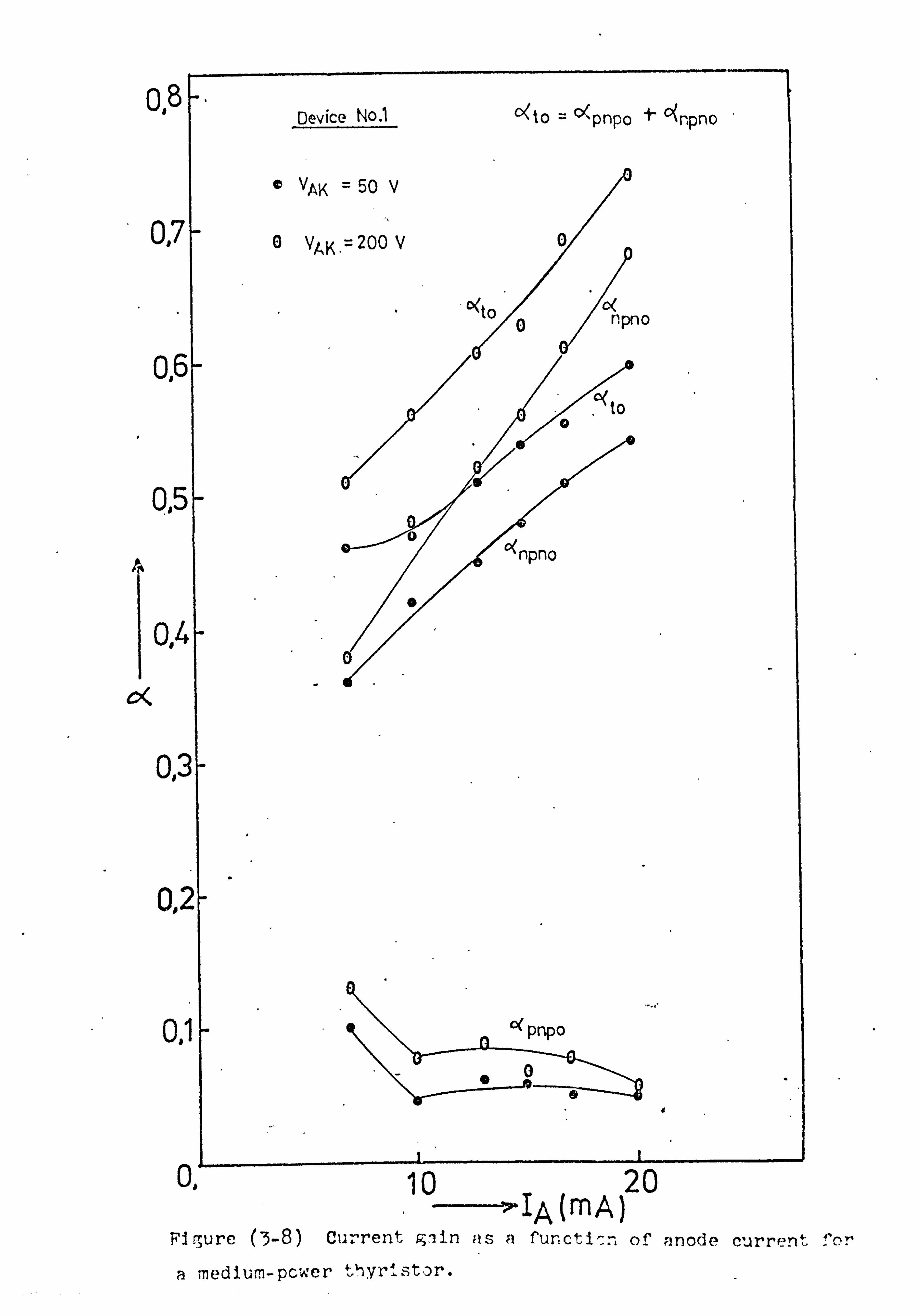
0,7
0.6
QJ5
0,4
001ý
U, 4
o;
Device N0.1 c<to = 0(pnpo i' 0(npno
VAK :' 50 V
0 VAK. = 200 V
Cýto/o
I
/` pno
to 0
.I
4
10 20 IA (M A)
Fi rrurc (3-8) Current 9,, iin ws, a f"lncti--n of anode current ror
a -medium, -pcwcr thyr'-stor.

1
(I) -
"
".
>
o0 11) II II
ci >>"-
a
If,
1'
E C%4

M
<
>5 C- EEEE 0 In Lo r- C)
If If lel
0 go. x0 do 0
I.
CL
cx
C:
flo.
C) CD 0)
C
cD
N . r:
C
1
p-
ew
LO % %
0

N
'4-
4;
1- �-4
CD Ln C)
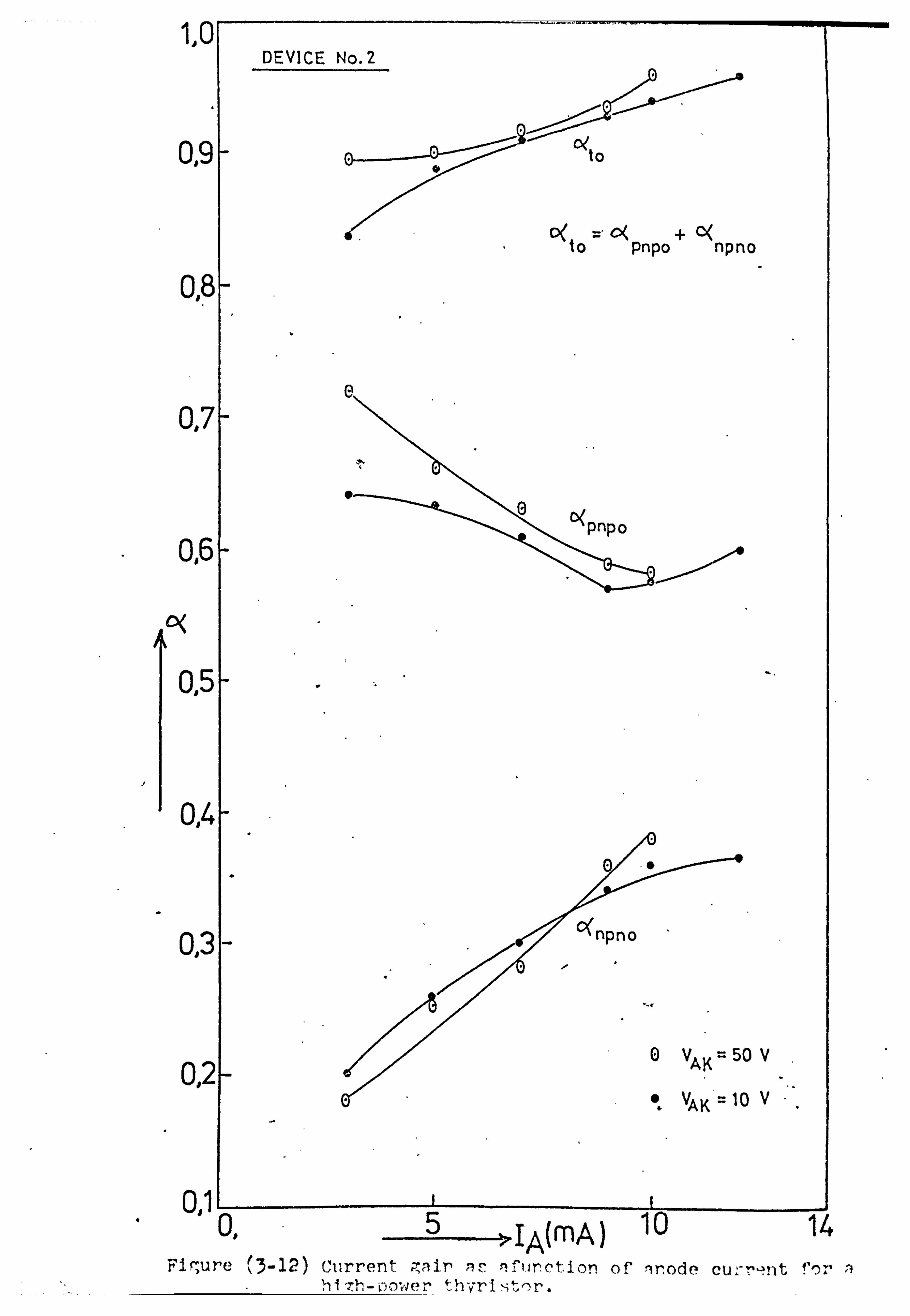
DrEVICE No. 2
0*9
to pnpo npno
o,, 8
0,7
0,6
Aý
0,5-
0,4-
0,3
0,2 VAK=50V
V =10 v AK
0,011 11 --1 4
IA(MA) 10 14 Fir�ure (3-12) Current gair lýý ir"-Irction of i-r. ode euý-r--j-it f-- a
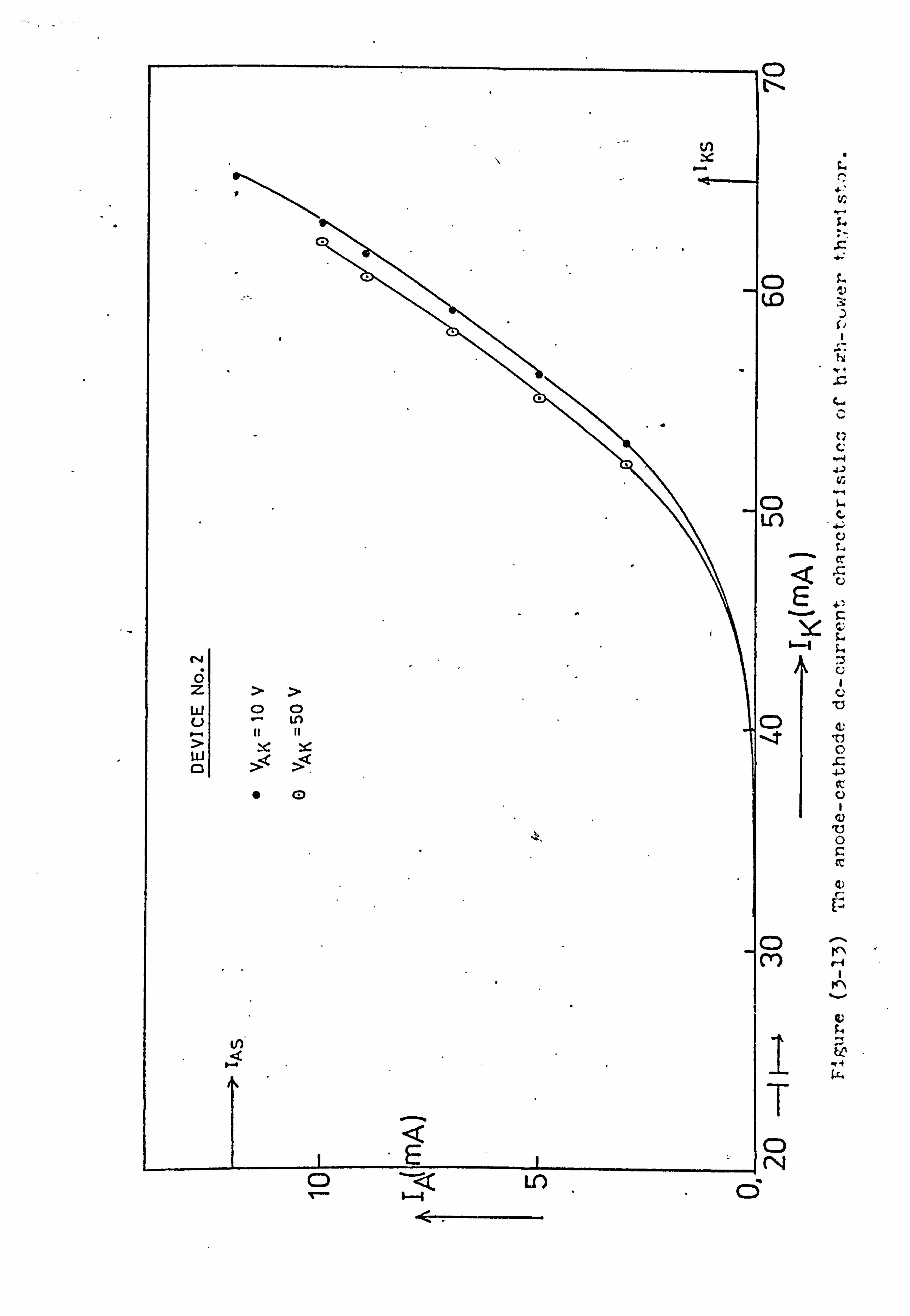
0 z w
LLJ 0
r4
>> o0
U) I, II
a,
if)
V. '
0 t-I
r.
LO
C) LO
aC
C) It
V 0
4) f'
CD
CD (N
ci -<Z Ln , cs
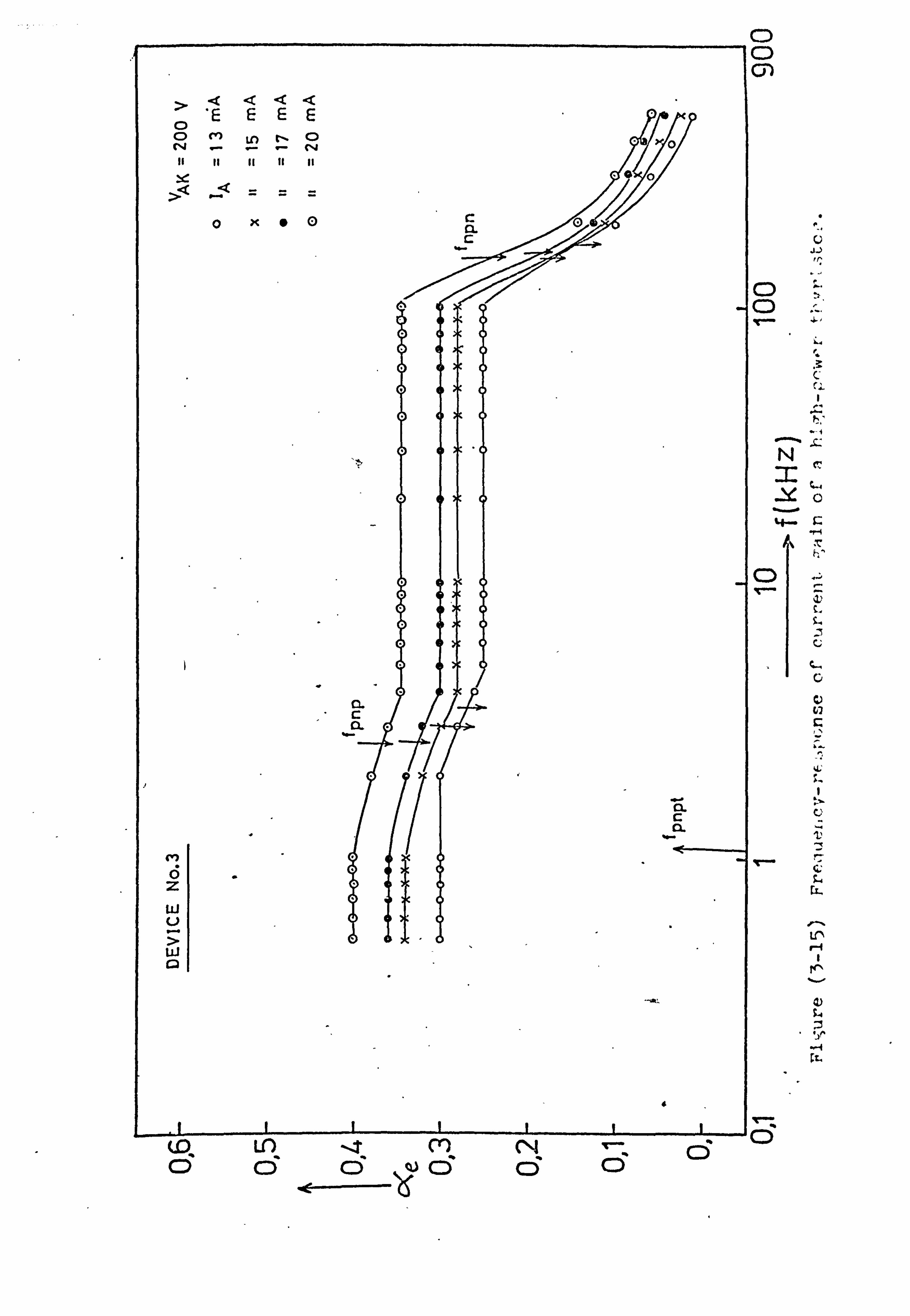
'E EEE
CL c cx
CL
I cx
0 z
> ul
Qc) %
U-) -4 C9 ft
CN 'Cý cs C) Cý C: ) C) C)
C: )
0 . 1. ) 'I;
C
T i% h, I
L
0
rv
C)
VN
4)

DEVICE No-3
Uot:
0"5
0�4
0., 3
0,, 2
081
VAK = 200 V
v AKý50 V
)npo
0(pnpo
a
08 5 10 15 20 -25 30 WMA
Figure (3-16) Current gain as a funcn lon of anode current of a high-power thyristor.

00
%. -a L-) Lr) < CN I

> E E E E E 0 LO Ln : m ý
It
>
7
C)
p-I C,
U-
*71
CD C)
(V
Z-, c C,
0 C 0.
II
%T
0 z Ld L)
LLJ 0
't
L) U)
N
i
Ix,
Co
C)
T-

o
0ii,
09
oa!
08
oj:,
0,1
0,2
,4 P"-IA(MA) Figure (3-19) current P, rntn is i "'-; nctJcr of inode
Qurrent fol I IOA th7rlstor (not gold-doped).

5
4 JA(
3
2
a
DEVICE NO. 4
VAK1* 50 V
inA) 'AS
IU 20 "'IK(mA)
Figure (3-20) , 71he anode-cathode dc-current charact. eristiý, cý
of a 10A thyristor (not gold-doped).

EE
0
CL c CL
T T
0X44
1A I
Lrk C)
C) C) cn
r-4
C 4.
�-4
A-
cD cD C
cc tý
-0 0---% r.
'I-
C
cD C
C
0-, r-4 cu
1 tr,
T-

0
DEVICE No. 5 i"o
e 0,8
006
004
Cýto E)
0
0- c<npno
0(to= c<pnpo+ 6ýnpno
VAK = 50 V
I.
-, I
5 IA mA 10
Figure (3-22) Current gain as m fun3tticn of nnode curret, 14',
for a 10A thyristor (cr, old-doped).
C
qpnpo
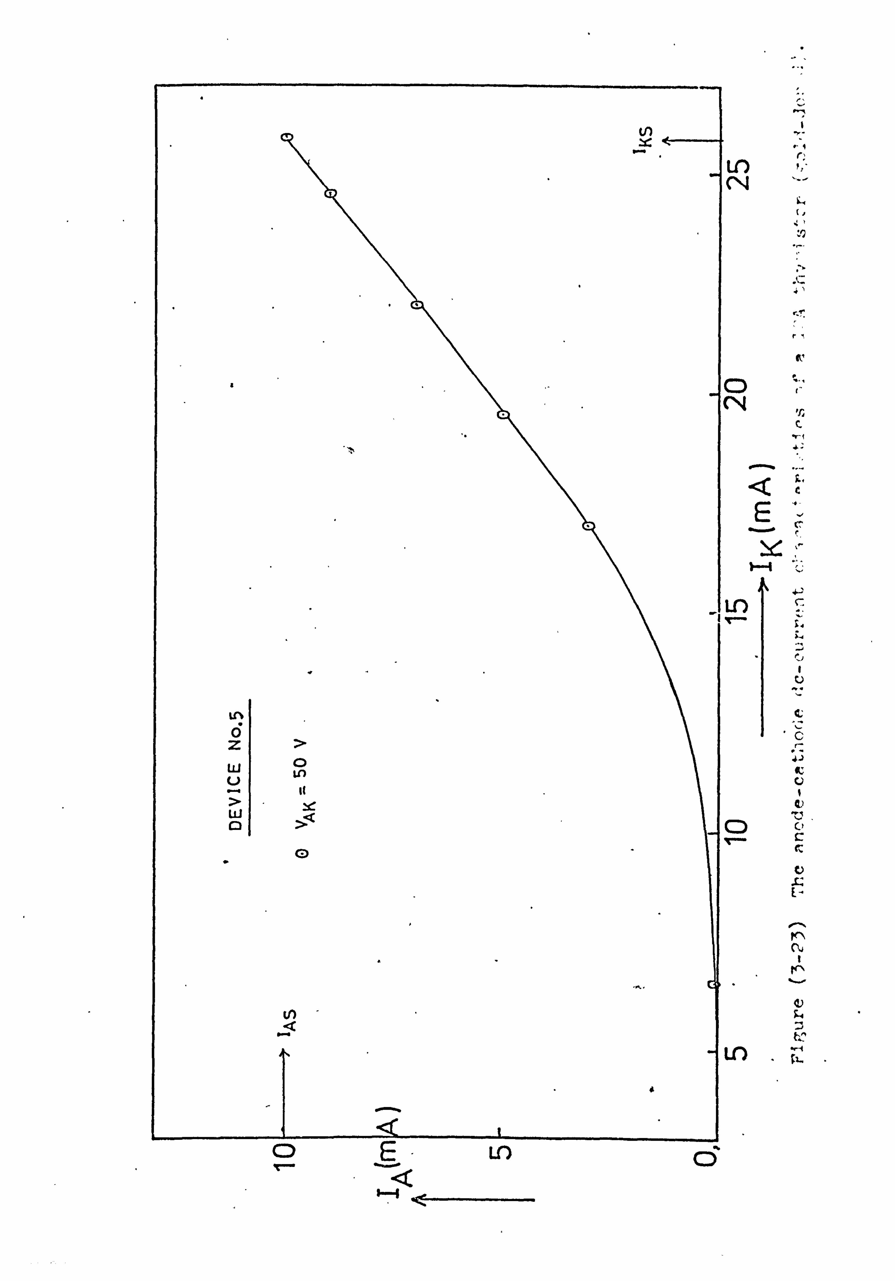
ul
z LLJ - L) U )
> LLJ
V)
LO -%
Ln
* 141,
C) (N
<c,
LO
C
"0
C)
C) V
C)
1
I-'
Lo

0,8 ý*
0,7
0.6 ý
09 ,
081
0,31
0,21
oil
09
DEVICE No. 1
VAK ' 50 V\ 9 MA. 0 cKpnpo
O<npno
0 o(to -1/\%
41
////0// //Z , l.
ý E), -
//7., 4E( IAý9MA \ \\ %% %1
00
0
PZ le 7
WO de
IM ,0y %% %%
\\
'0 11\tt
c( 1 zý
eý, %
ll-
to pnpo «
npn o
ýb
B
50 5
40 80 0 120 160 ITC Figure (4-1) Current gain as n function of tempermture.
for n medium-power th. vristor.
IA= 9 mA
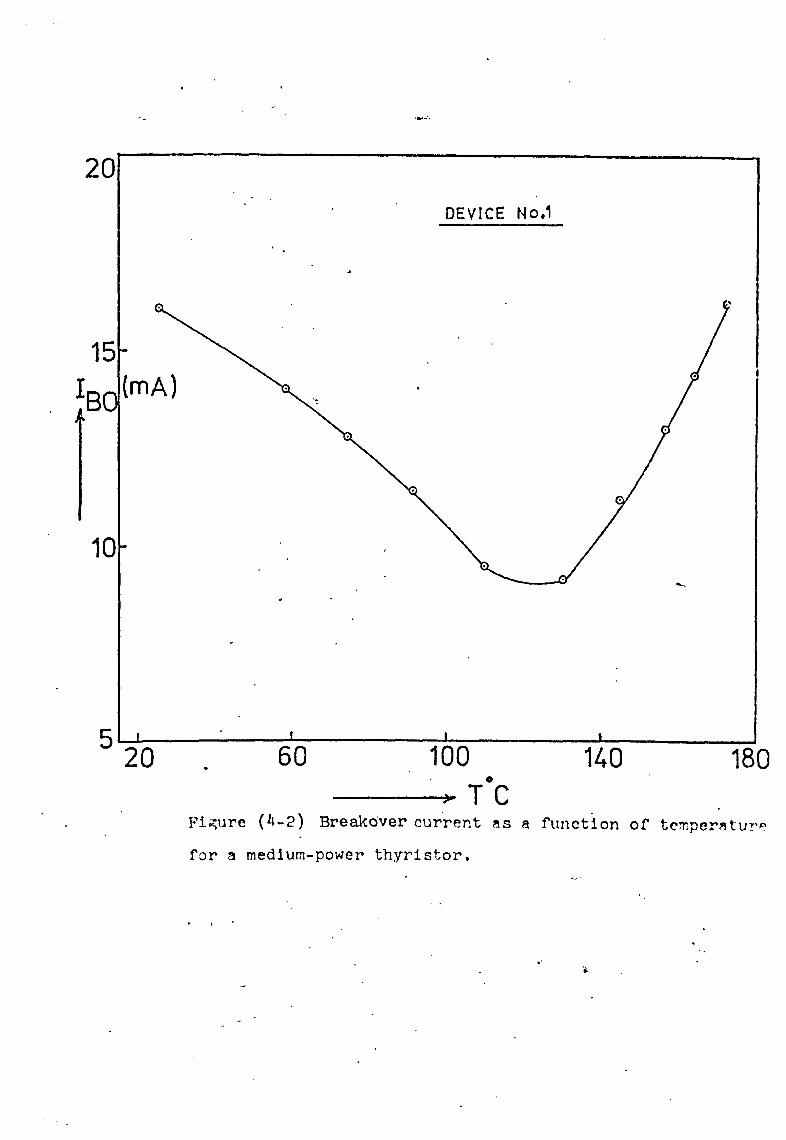
2
1 'B
DEVICE No. 1
5-
0 (MA)
TC Figure (4-2) Breakover current as a furiction of tcmperqtur, ý
for a medium-power tbyristor.

4C
3C
IG(
2C
10
DEVICE No. 1
0 'A m5 mA
=7 mA
=9 mA
mA)
. 40 . 80 0 120 -160 TC
Figure (4-3) Gate filing current as a function of
temperature for n rred iu-, n- power thyristor,.
I%k
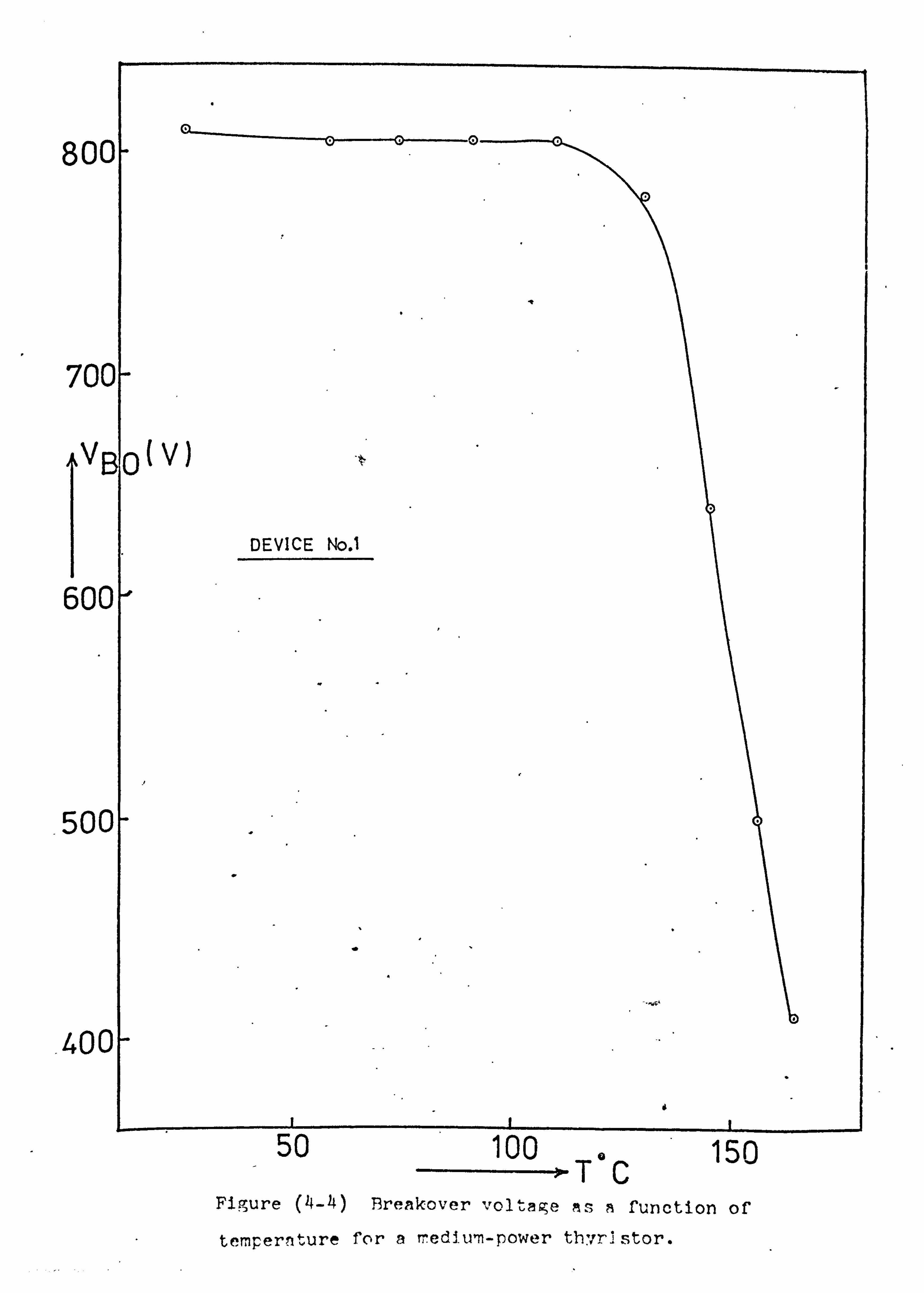
801
70
v
601
501
J. -0 ---0"
0-
BIO (V)
3[I
DEVICE No. 1
, 40OF
50 100 TaC,
150 Figure (4-4) Rremkover voltmge Rs 8 function of
ture for a rredlurn- power thyr! tempern, Istor.

1
0
0
0
oi
00
00
08
DEVICE No. 2
IA= GMA
IA=6mA
VAK ý SOV
0 CK npno
p n*p o
0 o( to.
CK c<pnpo + O<npno
3.
2
1
L it -J- rr
2 -.
I
.I
u Ou luu 140 T0C
Figure (4-5) Curr,! nt gairl as m function of tempernturc for a high-power thvristor.
'A =6 MA

21
IB A
1
DEVICE No. 2
(MA) 0
5- Z. ,
20 60 lUU 141 0 TC
Fjguýe Breakover current as a function of temperalture for n
high-power thyristor.

2
106
BC
1
0', [
DEVICE No. 2
20 bU 0 lUU -1 4L o, T
Figure (4-7) l3reakover volta- ,e as a function of
temperature for a high-po. -Mr thyristor.
4

109,
i
0)
0, '
oi
4ýc
VAK ý 50 V DEVICE No. 3
0 cKpnpo
v C>(npno . IA= 30 mA
0 o( to
- -0, 20
-0 _-- %1%. 1>
- -(-)- 17
0
IA =30tn A_
25
20
17
IA= 15MA
0,2[
oj
0
30
C-<to C>< pnpo + C<npno
I
Zu UU0 luu 4140 180 >- TC
Fi-, Y, u., -e (4-8) Current Tmin as A function of tempernture
for a high-power thyristor.

20
15
0
10
-
DEVICE No. 3
(MA)
20 60 T0
100 140 Figure (4-9) Breakover current as a function of tempý-r-ntl.. re
of 'a high-power thyristor,
4
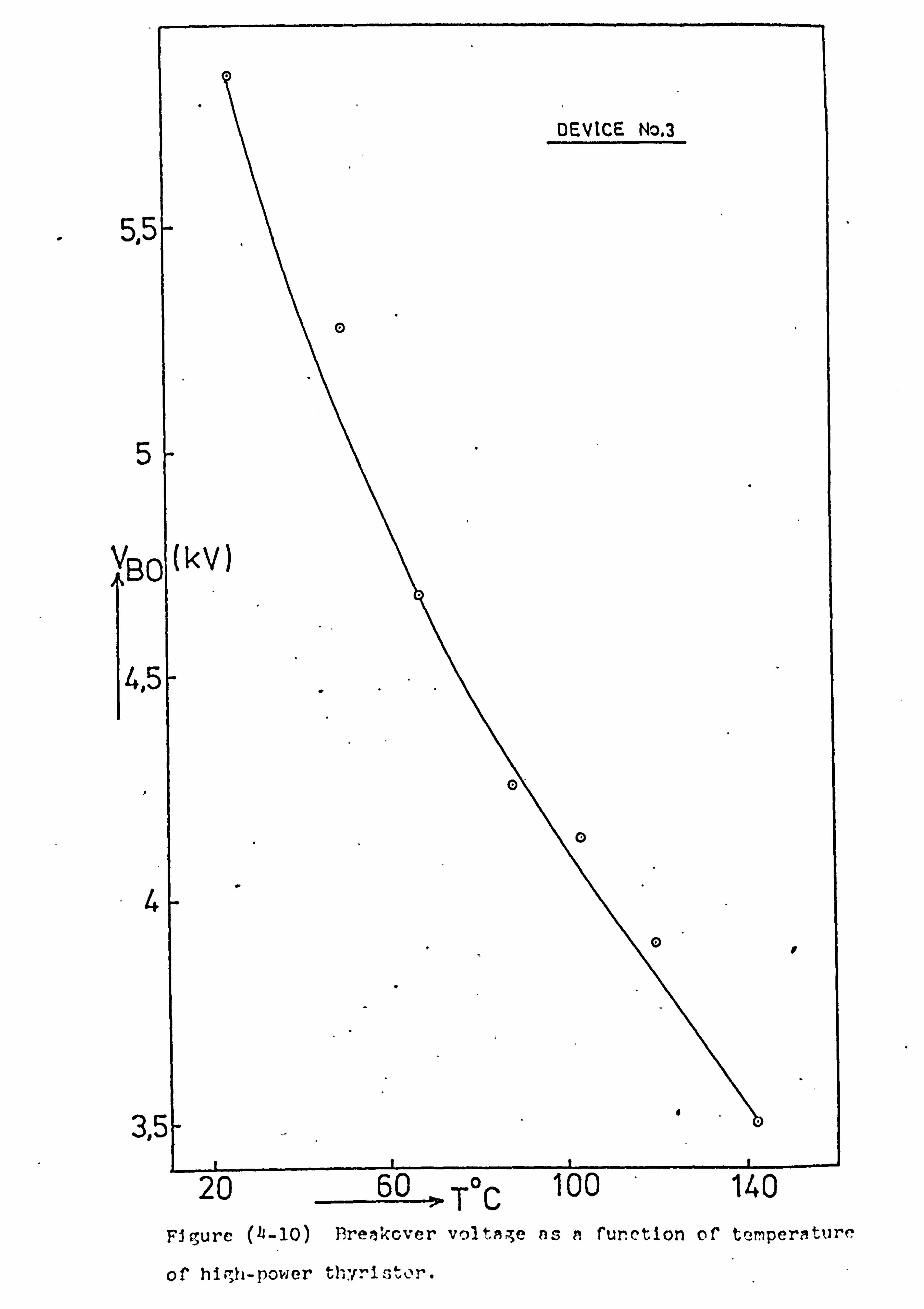
I
V , &IB
4p
3
DEVICE No. 3
0 (0)
0*
"m 20 60 . TOC 100 140
FJP,, ure (4-10) Premkover voltAge ns n furction or tempermture
of hi; ýh-power thyristor.

0,
od
Oa'
4e
03
1
0<
00!
0,
00
0,
n
JA =3 MA DEVICE No. 4
2.5 -E)-- -- -6- 2 E)
- -iý, ----- -- 0-..; -0
IA. = 3 MA
2.5
0--- ----- 111 .. Zýý, , ý-
Z 2
VAK 50 V
O(pnpo
b>", npno
oýto IA= 3 rnA
2.5 2
V'I 20 60 0
100 140 TC
FiZure ( 4-11) Current -,, ýin as n funct-ion of teinperature
for a 10A tlh, yristor (n,, t I- doped), .

3 IBO
2
1
0,
DEVICE NOA
(mA)
20 60 100' 140 -p- T0C
-Figure (4-12) Breakover current an a function of tempernt, jr-,:!
for a 1GA thyristor (not gold-doped).
500
BO
450
400
DEVICE No4
(MA)
20 60 100 . 140
0 TC Fir, ure (4-13) Iýreakover volta! -e ns a function of
for a 10A tbvristor (nutu rlold-doped).

TEXT CUT
OFF IN
ORIGINAL
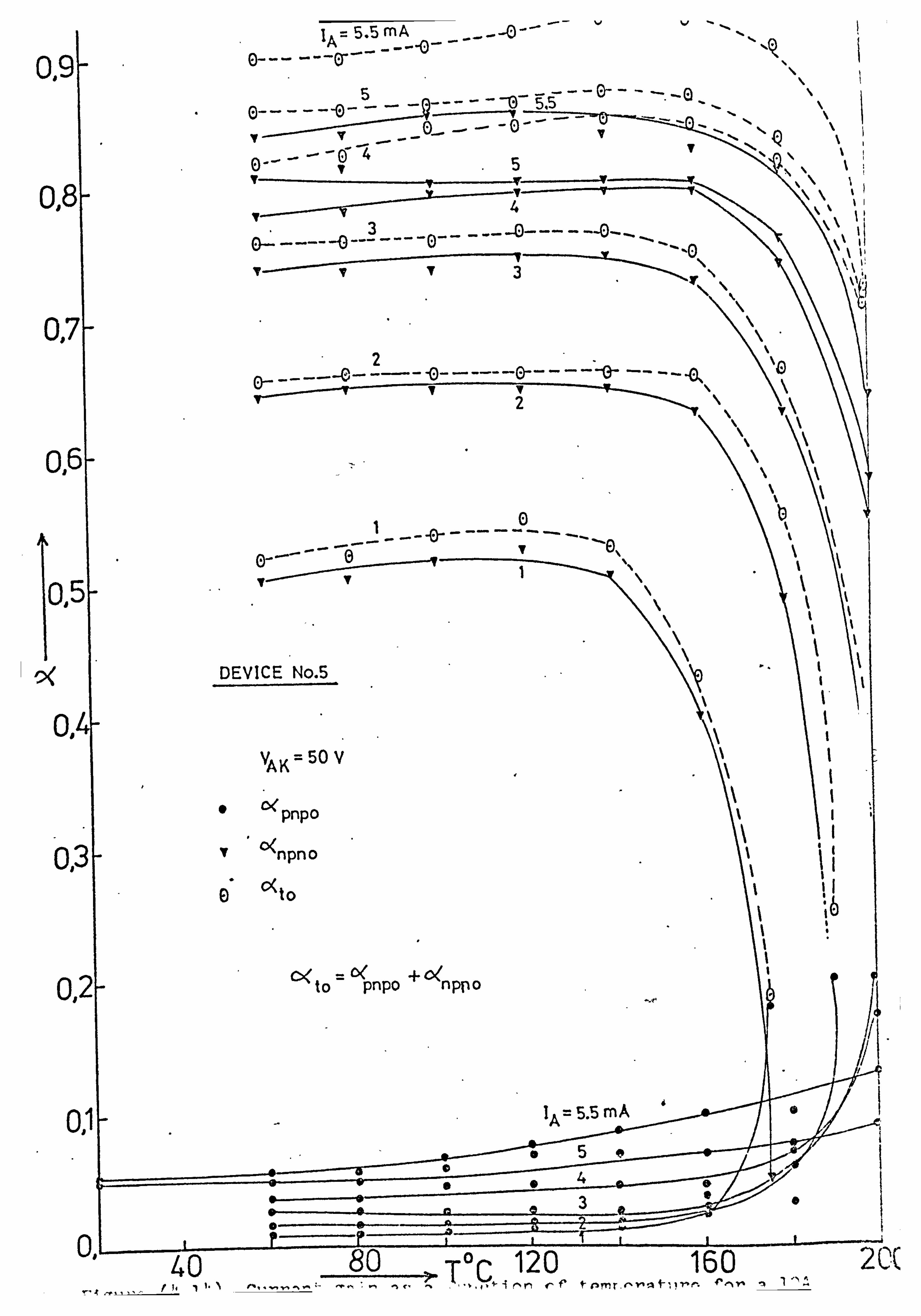
0,9
0,8
0,7
o, 6
0,, 5
09
0,3
0,2
O'l
JA= 5.5 MA
2: -7
0-- -ý-. 5%;
-------------
2
DEVICE No. 5
Ov VAK ý5
0 Oý pnpo I
npno
to
c< to ý pnpo + anppo
= 5.5 mA A=5
5 W .0
14
--- - ------- 3
o"I I T-r 1, -1111
40.80 ---- ),. TOG, 120ý
, ___ __ý_160_ _
--. i
f 1,1 1. ) ý- -- -- --i f, -ý lv., ý -Ir, rl f- TT rý mr-fIY. "II! 11, -. . -1. -. -

55,
VBI
501
4T
I- I It eI r"I-
20 60 0
100 140 ,-TC Figure (4-15) Breakover current Pis a function of temperature
for a 10A 'khyristor (gcld-doped).
180
20 60 100 140 180
Figure l3reakover voit-a-e aFý a function of temperature
-for a 10A thyristor (gold-dopnd).

15
ic
A
, A(
I
TC re for Figure (4-17) Anode current as a function of temperatu,
,I medium-po, -, er thyr! stor.

0"8
007
0
0*4
.0
0A
6EVICE NO. 1
VAK 'ý2 50 V
0 Oýpnpo
Tn pn o 0 cxý to
IT-
lF
IG =30 MA 9
1 =lOMA
EI,
11
ly
.7 C il-ý 20 bU -0 lUU 14U ýV-
C
Figure (4-18) Current gnin as a function of temperature for
a medium-power thyristor (at fixed Tr

C) CD t-I . 11
a 7)
0
Q:
to --f. -4
4- 1-)
IL
it0
x- t
C) ..
4-'
C.
C) AE

0,7-
09 5..
0 jý
.
0 �3.
0,2ý
)., lF
nL
DEVICE No. 6(S. D. )
VAK = 200 V
0( pnpo
npno
'A =14 MA
10
12
10
G
20 60 0 100 14U TC
Figure (5-2) Current clain is a function of tem-cerature for a
mediurm-power thvristor (shorted,, mitter).

1-1 M
M c
CL
EEEE In o In N cn m
0
Li ý ", li- (T-) (N X-Z (icý % CD Cs CD CD CD CD
'-I
F
C
.0
*.. ýo r
Z
U-A
tin --f Cr-
d

0,7
0,6
0,5
0,4
0,3
0,2
0,01
a
DEVICE No. 7( S. D. )
YAK = 200 V
C>(pnpo
C>(npno
IA=22 mA
...................... 17 15
10
IA =22 MA
20
17
is
10
IA
20 60 0 100 -140 -o TC
Figure (5-4) Current gain as a function of temperature ror
iedium-power thyristor (shorted-emitter).

550
500
VBO(
450
DEVICE No. 7 (S. D. )
20 60 100 . 140
0 TC Pigure (5-5) Breakover volta. re as a function of temperature
-ter) for a medium-power thyristo-A (snorted-em. 4A. 4.
6
i
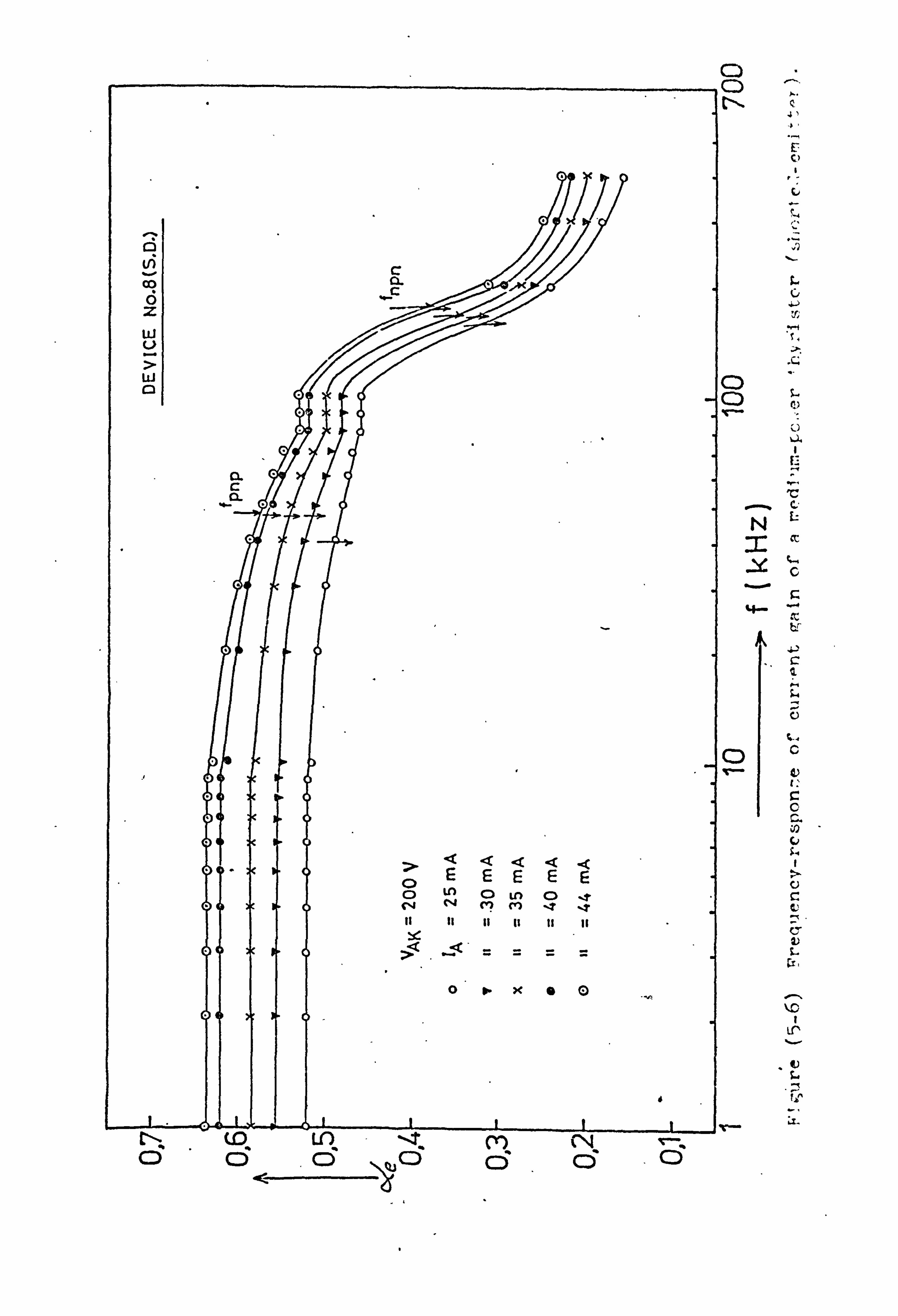
co
6 z
w
w
CL
EE 0 C) Ln
0
L-", ý. i *ýý CNIL T-.
Q -:
CD
14-
C
p.,
0
ol
C C. : 1)
C)
C. )
2)
\Z 1
tr
.v

DEVICE No. 8 (S. D. )
0,7- VAK 1'200 V
Oe'pnpo
Oýnpno
0,, 6
0,5
0,4
0ý
0,3
0,2 1
0*1
'A=35MA
30
25
20
15
. 51
O'l IIIIIIV _* -1
40 80 120 160 ,0 TC
Figure (5-7) Current aain as a function of tempersture for
ted-c-ritter medium-power thyristor (short
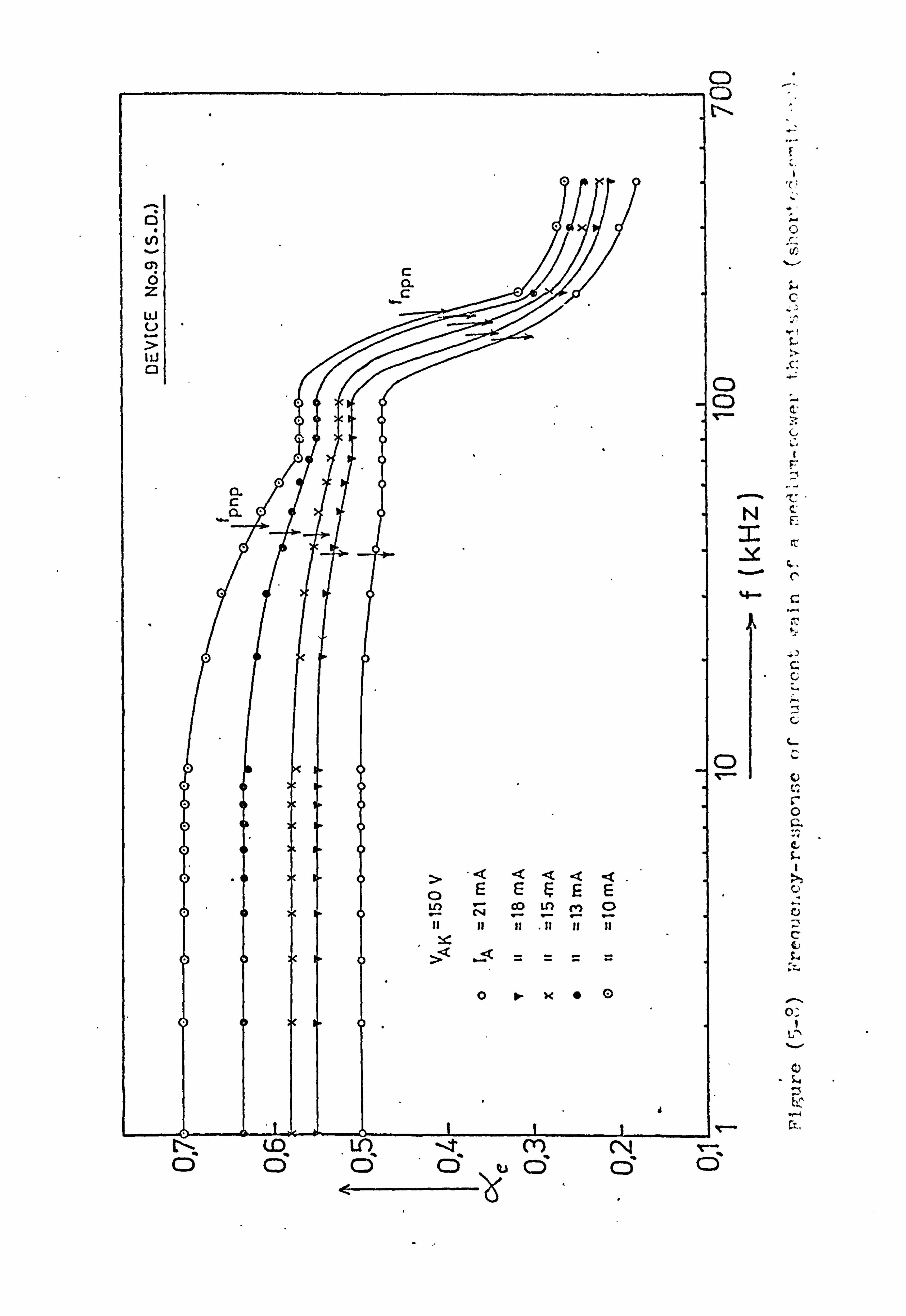
C)
C)
0---%
CD
T-
F! - lu - c: F--
4ý
91
. -I 0-
000 qÖ cc

097
0#, "'
O<
o, z
DEVICE No. 9 ( S. D. )
VAK ý'150 V
cý plip-0
C<npno
V14MA
.................. . ....................... .............. 12
10
6
0,3-
0,2
081
'A =14mA
6 4
08 1111..
-I 20 60 0
100 140 c
Figure (5-9) Current gnin as a function of I empera ture
for a medium-power thyristor (shortvd-eTitter).

550
500
VBO
450
400
DEVICE No-9 (S. D. )
20 60 0 100 140 TC
Figure (5-10) Breakover voltage as a , nunction o, '. * tempernture
fcr a rrcdium-powcýr thyristor (shorted- emi't te f, )

C)
r
Ili
L4
-4
cD '
0
N Ir
L
'I- C
r
'S
C
Q C C- C,,
C
C)
0-ý
r-4
LL.
__j T-- -b
CD co LO Ln -%T CN V-.. % ft % ft
Q) % ft C) - CD C) CD CD %*-; - C) C)

of
Oa
1
DEVICE No. 10
VAK=150 V
(><pnpo
c-'npno
Sý
5-
4.
3.
0,2
C
Ja
-
IA ý12 MA
10
=12 mA
____. 4
I
20 - 60 0
100 140 !.:;, - TC
Current 7, nin ns n function of terrperAlture fr'cr
Tedium-power thvristor (no'. sý, orted-c. rlltter).
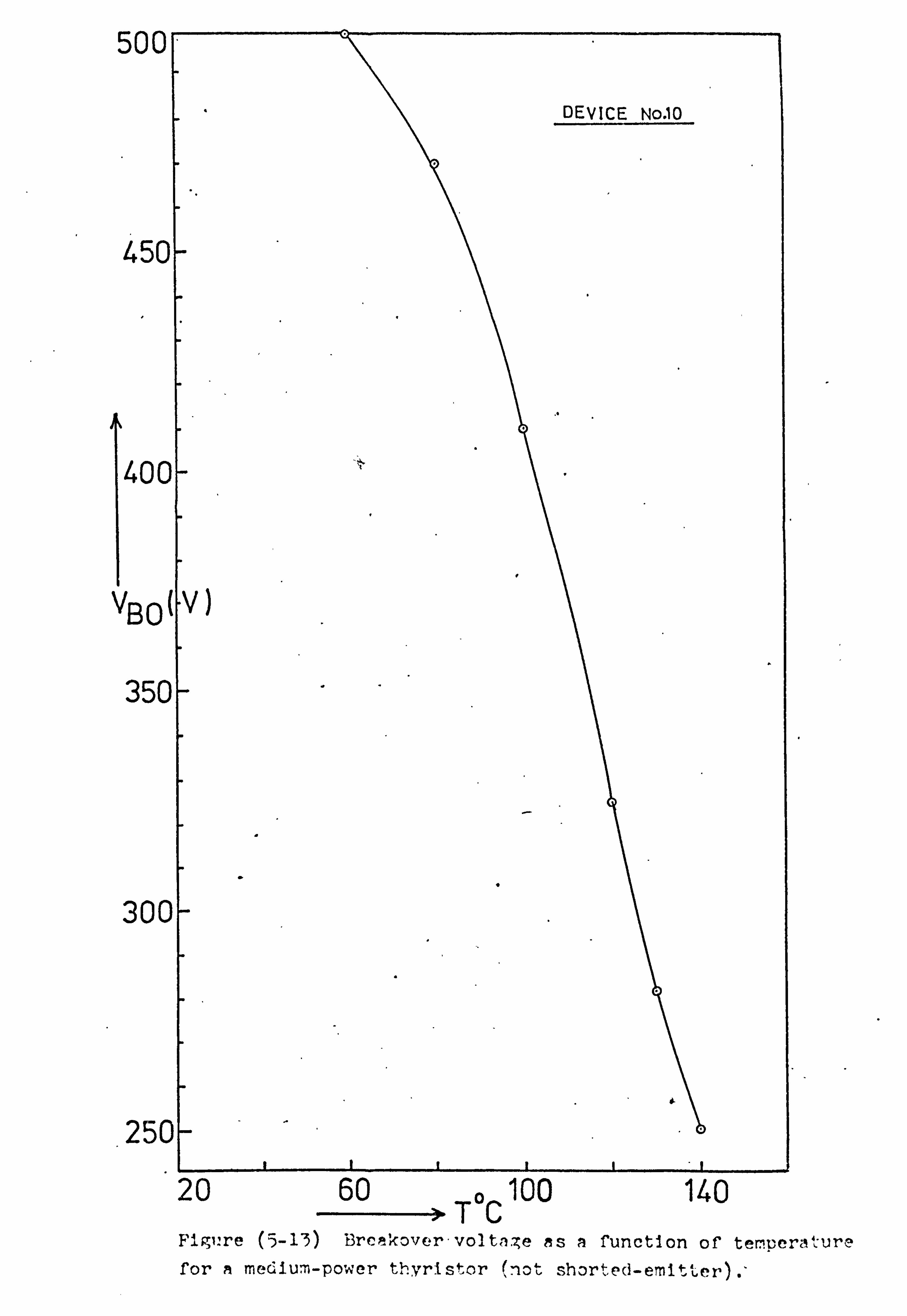
500
450
400
VBO 1
350
30C
25C
DEVICE No-10
20 60 * TOC
100 140 Figure (5-13) Brcakover, volta. -4e ns a functlon of tempermt-ure for n medium-power thyristor (nott shorted-emitter). '

Cj
Ci.
in.
Iý
< EEEE Lo (: ) U-) oc)
mm it 11
$P x0
U) C) c) r4) C: )
mile ci
C: ) V-1
4-3
G,
C)
T;
tr
cy
CN T-.
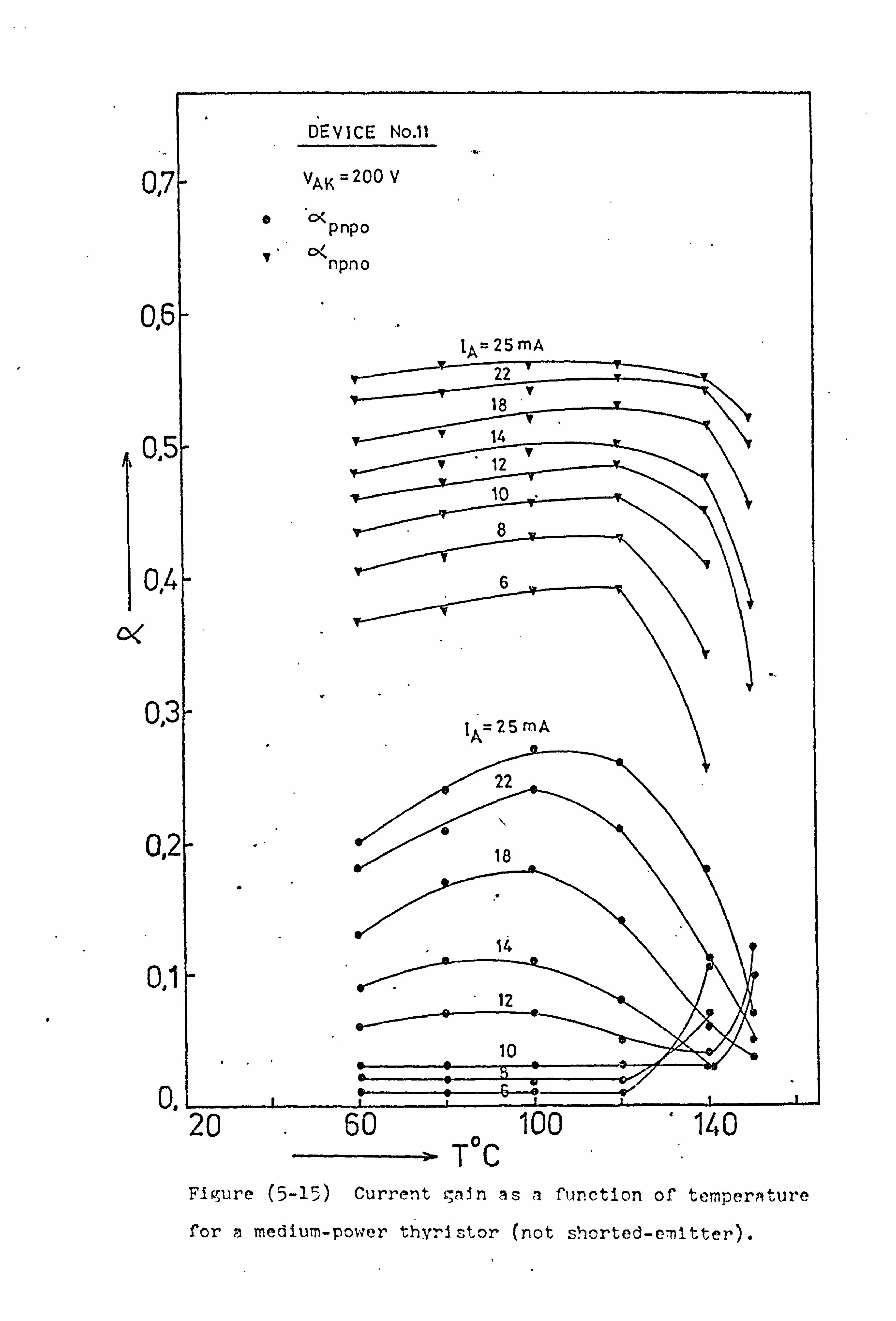
0
0,7
0,6
0,5
0#4
0��. '
0
1, le
O'l
0
DEVICE No. 11
VAK ý 200 V
0( pnpo
npno
IA=25mA 22 T
18 . ................ 14
12
10
8
6
JA=25MA
22
18
12
10
20 60 100 140 TDC
Figure ("D-11D) Current L, -, iJn as i function of tempern'llure
for n medium-power thyristor (not shorted-emitter).

55C
500
450
v( BO
400
350
300
DEVICE Noll
20 60 0 100 140
Figure (5-16) f3reAkover voltage as a functicn of temperinturc, for a mediull-power th. yrlstor (not shorted-e-nitter).

C) CD t*--.
L
'a
C14 0
z
w C-, > w
c C.
0
C
"L
. ý. I
cD
U
a c
%"
ix -
c 0-6-- rj cc
-4
C
> C C
II
><
EEE to Cl Lo C4 CY) m
If
0
6
L
C)l
UJ LO CN C) C) CD CD CD

0,7
0,6
005
0,4
C< ojý
VAK ý 200 V
0 cýýpnpo
T C><np no
IF
'A = 35 mA
0, -j
0.0
zu OU -lUU 14U 0 TC
Figure (5-18) Current gnin as i function of temperature fýýr
a mcdium-ý)cwer thvristor, (not -horted-e-nitter).
DEVICE No. 12
1.35 MA
ppI -aAaaSa

E E
LO
rn LD LO -4 ry". CD CD CD CD CD CD CD
C)
o o
C-
I,
St
C C';
01.
I..,

0,7
0,6
005
o, z,
D< otlý
0j"
00
C
DEVICE NO. 13
VAK = 150 v
C4 npno
pnpo
IA=14mA
12
............ ........
V 14 MA
1- 6 4
20 60 0 100 140
rva TC Fi 7,, u re Current gain as a function of tempernture
for a medium-power th*ýrlstor (not shorted-emitter).

5.11. NO-5. D.
"'Room Temp.
61 ill VAK ý ZOO V
VAK'--150
0.4 0.5
0(npno
IA ý-10 MA
0,3 0,4
` D(np no
S. D. N 0. S. D.
0
T=60 C
91 10 VAK 150 V
0,4 0,5
np no
IA=10 MA
ll 16 VAK 200 V
0,4 015
c<npno. Fi. gure (5-21) Histogrammatic, dingram of current gain of transistor secc tion of thyri, -)tcr at different temperatures.

, 5. lD NO. S-D,
0
T=80 C
9110 VAK=150 V
O's 0.96
'(: '<npno
'A=10 MA
6 Ill VAK = 200 V
9 0,4 O's
ý ': 'ýnpno
I
S. D. NO. S. D.
0
T=100 C
VAK : -150
10 19
0,5 0,6
O<npno
,A =10MA
61 11 VAK = 200 V
0,4 0,5'
C< npno
cont. of Flolure (5-21).

S. D. NO. S. D.
IP t.
T =120 0C
v AK: -"50 V
0,5 0,6
o< npno
'A=10MA ,
61 VAK = 200 V
0,4 0,5
(><npno
S. D. NO-5-D.
Ii
T =140 0C
v =150 V AK 10
0,4 O's
rip no
A -ý10 M*A
6 v AK=200 V
Oj3 0,4 O's
c$< np no
cont. of Figure (5-21).

---C
-
tl- to to 0
it C14
V) m .4
0 so, . 44
Q cm - .4
LO CD T- LO x

Ln
%. -f %-. of
OD (C)
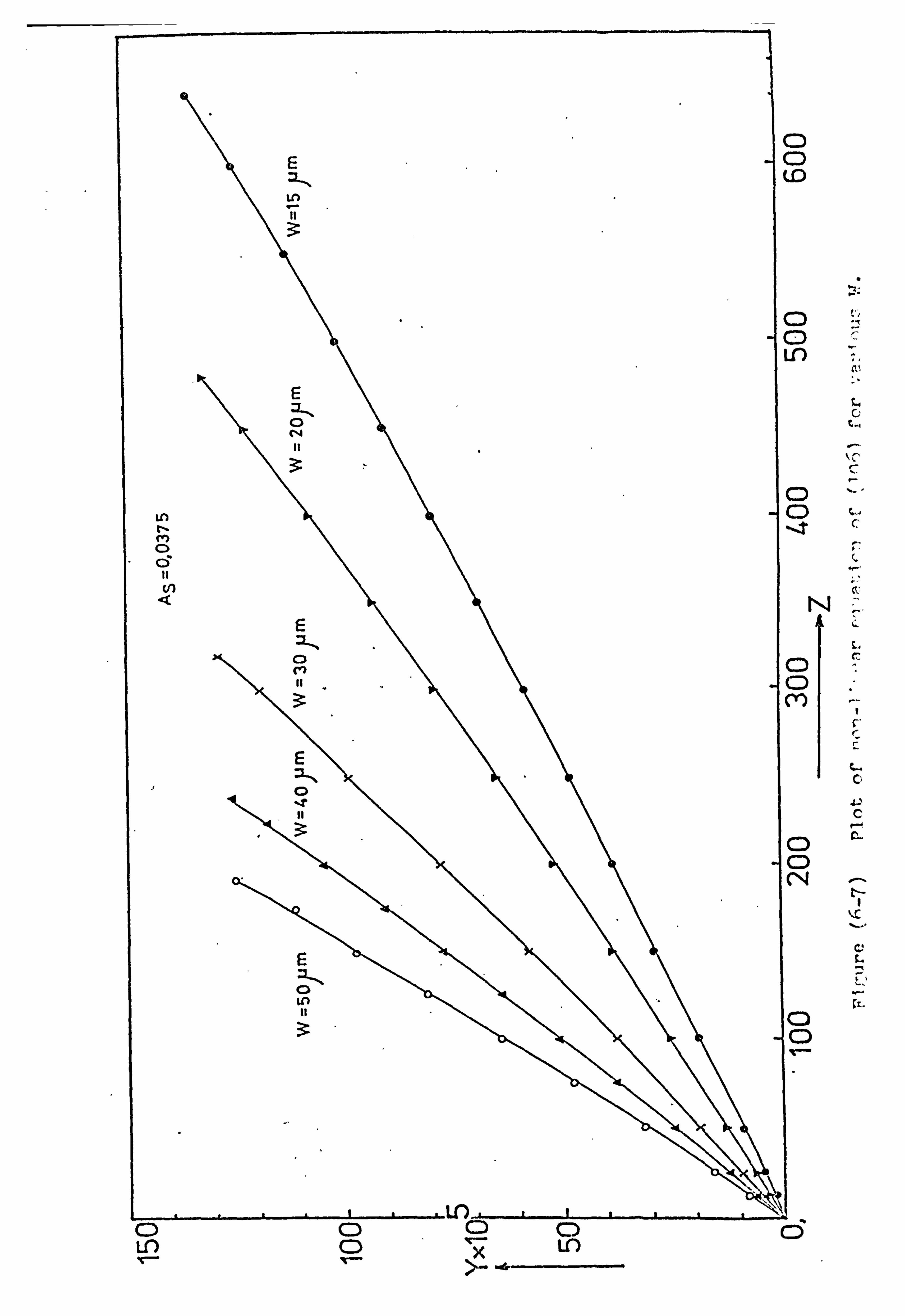
C) C) LO
0 C) Lr)
CD C) -T
N
C) CD CY)
C)
C)
r
C
C
c
c r C
L C
4-' C
r4
11C
CD Lf) x-
C: ) CD C) qr- LO x >- -mer
C)

0 ý)
80
75
IL(p 16
70
65
As= 0,0375
AS=0,0675
M/cm) As= 0,125
AS=0,2'
6
U" 10 20 30 40 50 60 (ýM)
Figure (6-8) Variaticn of hoie current TL at (I-A. ) W at constant AS*

C)
C
ll-ý
0
Tu jo siTun UT uoTqu. Ialýui&Z)Uoj
CT) C)
CC) C)
tll-. C) Loc)
T- - Ir- T- V-

j
cn
Co
cý
C) C) Q C) C'14 (Y) V)
I
b/jN E; jjun uuulz! jjoa uT I-ellua4ocl
E M,,
_c 4--
Z,
e)
0
P4

10-
1 (-7
I CL
C
C4 0ý co 5
tp
i C c 03
a) w
0 x .4
CD CD CD L--i 'C
*b/'LX GOUZIOA UUWZZIOZ UT luTqu; )ý4od
V
r-
0- -:
9- C,
ft C)

9 10
10 7
C
LI
. 1-I
rl
c -r-q 4-3
ic
VC B 1.02 v
VE B Q9 V
0.8 v
It - 0.7 v
it - 0.6 V
x
)F .I
Uj, UA Depthojrri) U'd Figure (7-1P) Nom. valized electron density distiblition in units of nV

109
107
-4
0
m 4. -)
10 "r
10
ic
c
Depth (ýim) Figure (7-13) Normalised hole density dist 'ribution
in units of ni,