Embed Size (px)
Citation preview

IPC-6012Bwith Amendment 1
Qualification and Performance
Specification for Rigid
Printed Boards
ASSOCIATION CONNECTINGELECTRONICS INDUSTRIES
3000 Lakeside Drive, Suite 309S, Bannockburn, IL 60015-1249Tel. 847.615.7100 Fax 847.615.7105
www.ipc.org
IPC-6012Bwith Amendment 1January 2007 A standard developed by IPC
Supersedes IPC-6012BAugust 2004
The Principles ofStandardization
In May 1995 the IPC’s Technical Activities Executive Committee (TAEC) adopted Principles ofStandardization as a guiding principle of IPC’s standardization efforts.
Standards Should:• Show relationship to Design for Manufacturability
(DFM) and Design for the Environment (DFE)• Minimize time to market• Contain simple (simplified) language• Just include spec information• Focus on end product performance• Include a feedback system on use and
problems for future improvement
Standards Should Not:• Inhibit innovation• Increase time-to-market• Keep people out• Increase cycle time• Tell you how to make something• Contain anything that cannot
be defended with data
Notice IPC Standards and Publications are designed to serve the public interest through eliminating mis-understandings between manufacturers and purchasers, facilitating interchangeability and improve-ment of products, and assisting the purchaser in selecting and obtaining with minimum delay theproper product for his particular need. Existence of such Standards and Publications shall not inany respect preclude any member or nonmember of IPC from manufacturing or selling productsnot conforming to such Standards and Publication, nor shall the existence of such Standards andPublications preclude their voluntary use by those other than IPC members, whether the standardis to be used either domestically or internationally.
Recommended Standards and Publications are adopted by IPC without regard to whether their adop-tion may involve patents on articles, materials, or processes. By such action, IPC does not assumeany liability to any patent owner, nor do they assume any obligation whatever to parties adoptingthe Recommended Standard or Publication. Users are also wholly responsible for protecting them-selves against all claims of liabilities for patent infringement.
IPC PositionStatement onSpecificationRevision Change
It is the position of IPC’s Technical Activities Executive Committee that the use and implementationof IPC publications is voluntary and is part of a relationship entered into by customer and supplier.When an IPC publication is updated and a new revision is published, it is the opinion of the TAECthat the use of the new revision as part of an existing relationship is not automatic unless requiredby the contract. The TAEC recommends the use of the latest revision. Adopted October 6, 1998
Why is therea charge forthis document?
Your purchase of this document contributes to the ongoing development of new and updated industrystandards and publications. Standards allow manufacturers, customers, and suppliers to understandone another better. Standards allow manufacturers greater efficiencies when they can set up theirprocesses to meet industry standards, allowing them to offer their customers lower costs.
IPC spends hundreds of thousands of dollars annually to support IPC’s volunteers in the standardsand publications development process. There are many rounds of drafts sent out for review andthe committees spend hundreds of hours in review and development. IPC’s staff attends and par-ticipates in committee activities, typesets and circulates document drafts, and follows all necessaryprocedures to qualify for ANSI approval.
IPC’s membership dues have been kept low to allow as many companies as possible to participate.Therefore, the standards and publications revenue is necessary to complement dues revenue. Theprice schedule offers a 50% discount to IPC members. If your company buys IPC standards andpublications, why not take advantage of this and the many other benefits of IPC membership aswell? For more information on membership in IPC, please visit www.ipc.org or call 847/597-2872.
Thank you for your continued support.
©Copyright 2007. IPC, Bannockburn, Illinois. All rights reserved under both international and Pan-American copyright conventions. Any copying,scanning or other reproduction of these materials without the prior written consent of the copyright holder is strictly prohibited and constitutesinfringement under the Copyright Law of the United States.
IPC-6012B with Amendment 1
Qualification and
Performance Specification
for Rigid Printed Boards
Developed by the Rigid Printed Board Performance Specifications TaskGroup (D-33a) of the Rigid Printed Board Committee (D-30) of IPC
Users of this publication are encouraged to participate in thedevelopment of future revisions.
Contact:
IPC3000 Lakeside Drive, Suite 309SBannockburn, Illinois60015-1249Tel 847 615.7100Fax 847 615.7105
Supersedes:IPC-6012B - August 2004IPC-6012A with
Amendment 1 - July 2000IPC-6012A - October 1999IPC-6012 - July 1996IPC-RB-276 - March 1992
ASSOCIATION CONNECTINGELECTRONICS INDUSTRIES

FOREWORD
This specification is intended to provide information on the detailed performance criteria of rigid printed boards. It super-sedes IPC-6012B and was developed as a revision to those documents. The information contained herein is also intended tosupplement the generic requirements identified in IPC-6011. When used together, these documents should lead both manu-facturer and customer to consistent terms of acceptability.
IPC’s documentation strategy is to provide distinct documents that focus on specific aspects of electronic packaging issues.In this regard, document sets are used to provide the total information related to a particular electronic packaging topic. Adocument set is identified by a four digit number that ends in zero (0) (i.e., IPC-6010).
Included in the set is the generic information, which is contained in the first document of the set. The generic specificationis supplemented by one or multiple performance documents, each of which provide a specific focus on one aspect of thetopic or the technology selected.
Failure to have all information available prior to building a board may result in a conflict in terms of acceptability.
As technology changes, a performance specification will be updated, or new focus specifications will be added to the docu-ment set. The IPC invites input on the effectiveness of the documentation and encourages user response through completionof ‘‘Suggestions for Improvement’’ forms located at the end of each document.
IPC-6011GENERIC
HIERARCHY OF IPC QUALIFICATION ANDPERFORMANCE SPECIFICATIONS
(6010 SERIES)
IPC-6012RIGID
IPC-6013FLEX
IPC-6015MCM-L
IPC-6016HDI
IPC-6018HIGH
FREQUENCY

AcknowledgmentAny document involving a complex technology draws material from a vast number of sources. While the principal membersof the Rigid Printed Board Performance Specifications Task Group (D-33a) of the Rigid Printed Board Committee (D-30)are shown below, it is not possible to include all of those who assisted in the evolution of this standard. To each of them,the members of the IPC extend their gratitude.
Rigid Printed BoardCommittee
Rigid Printed Board PerformanceSpecifications Task Group
Technical Liaisons of theIPC Board of Directors
ChairSusan S. HottRobisan Laboratory Inc.
Vice-ChairVicka WhiteHoneywell Inc. - Air Transport Systems
ChairMark BuechnerBAE Systems
Vice-ChairRandy R. ReedMerix Corp.
Peter BigelowIMI Inc.
Sammy YiFlextronics International
Rigid Printed Board Performance Specifications Task Group
Robyn L. Aagesen
Sheila C. Akins, M-Flex,(Multi-Fineline Electronix Inc)
Allan Pat Anderson, The BoeingCompany
Franklin D. Asbell
Gail Auyeung, Celestica InternationalInc.
Mary E. Bellon, Boeing SatelliteSystems
Eric Benjamins, MicrotekLaboratories
Wendi Boger, Dynamic Details, Inc.
Gerald Leslie Bogert, Bechtel PlantMachinery, Inc.
Scott A. Bowles, Hallmark CircuitsInc.
Ronald J. Brock, NSWC - Crane
Elaine Brown, Lockheed MartinCorporation
Jennifer Burlingame, Cisco SystemsInc.
Dennis J. Cantwell, Printed CircuitsInc.
Byron Case, L-3 Communications
Pei-Liang Chen, Shanghai PrintronicsCircuit
Phillip Chen, L-3 CommunicationsElectronic Systems
Denise Chevalier, Amphenol TCS
Christine R. Coapman, DelphiElectronics and Safety
Dan Colvin, Tyco PCG/LoganDivision
David J. Corbett, Defense SupplyCenter Columbus
Dennis DeBord, Nortel NetworksCenter 1
C. Don Dupriest, Lockheed MartinMissiles and Fire Control
Theodore Edwards, Dynaco Corp.
Alan Exley, Cosmotronic
Thomas G. Farrell, UnderwritersLabs Inc.
Gary M. Ferrari, C.I.D.+, FTGCircuits
Dennis Fritz, MacDermid, Inc.
Lionel Fullwood, WKK DistributionLtd.
Mahendra S. Gandhi, NorthropGrumman Space Technology
Thomas F. Gardeski, E. I. du Pont deNemours and Co.
Michael R. Green, Lockheed MartinSpace Systems Company
Hue T. Green, Lockheed MartinSpace Systems Company
Ken Greene, Siemens Energy &Automation
Philip M. Henault, RaytheonCompany
Aram Henesian, Lockheed MartinSpace Systems Company
Michael E. Hill, Colonial CircuitsInc.
Shelly Hsu, Compeq ManufacturingCo. Ltd.
Bryan James, Rockwell Collins
Todd Jarman, L-3 Communications
Ted J. Jones, NSWC - Crane
Thomas E. Kemp, Rockwell Collins
Jason Koch, Robisan Laboratory Inc.
Nick Koop, C.I.D., Minco ProductsInc.
Leo P. Lambert, EPTAC Corporation
Michael G. Luke, C.I.D. RaytheonCompany
Clifford R. Maddox, The BoeingCompany
Chris Mahanna, Robisan LaboratoryInc.
Kenneth J. Manning, RaytheonCompany
Rene R. Martinez, NorthropGrumman Space Technology
Brian C. McCrory, Delsen TestingLaboratories
David R. McGregor, E. I. du Pont deNemours and Co.
Chetan Mehta, C.I.D., One SourceGroup
Peter B. Menuez, L-3Communications
Renee J. Michalkiewicz, TraceLaboratories - East
January 2007 IPC-6012B with Amendment 1
iii

Scott Montgomery, The BoeingCompany
Susan Morgana, United Technologies
John H. Morton, C.I.D., LockheedMartin Corporation
Mary Muller, Crane Aerospace &Electronics
Bob Neves, Microtek Laboratories
Benny Nilsson, Ericsson AB
Steven M. Nolan, C.I.D.+, LockheedMartin Maritime Systems
Debora L. Obitz, Trace Laboratories -East
William A. Ortloff, Sr., RaytheonCompany
Michael W. Paddack, The BoeingCompany
J. Lee Parker, Ph.D., JLP
Mel Parrish, STI Electronics, Inc.
Stephen G. Pierce, SGP Ventures,Inc.
Visa Ruuhonen, Nokia Oyj
Karl A. Sauter, Sun MicrosystemsInc.
Joseph C. Schmidt, Raytheon MissileSystems
Kenneth C. Selk, Northrop GrummanSpace Technology
Bob Sheldon, Pioneer Circuits Inc.
Russell S. Shepherd, MicrotekLaboratories
Lowell Sherman, Defense SupplyCenter Columbus
Hans L. Shin, Pacific TestingLaboratories, Inc.
Roger Su, L-3 Communications
Dung Q. Tiet, Lockheed MartinSpace Systems Company
Jim J Vanden Hogen, Plexus Corp.
Crystal E. Vanderpan, UnderwritersLaboratories Inc.
Ronnie Walker, Northrop Grumman
Clark F. Webster, ALL Flex Inc.
Vicka White, Honeywell Inc.
Dewey Whittaker, Honeywell Inc.
John E. Williams, RaytheonCompany
David L. Wolf, Conductor AnalysisTechnologies, Inc.
Anthony Wong, NASA JohnsonSpace Center
Scott Worley, NASA Marshall SpaceFlight Center
IPC-6012B with Amendment 1 January 2007
iv

Table of Contents
1 SCOPE ........................................................................ 1
1.1 Statement of Scope ............................................. 1
1.2 Purpose ................................................................ 1
1.3 Performance Classification and Type ................. 1
1.3.1 Classification ....................................................... 1
1.3.2 Board Type ......................................................... 1
1.3.3 Selection for Procurement .................................. 1
1.3.4 Material, Plating Process and Final Finish ........ 1
1.4 Definition of Terms ............................................ 2
1.5 Interpretation ....................................................... 2
1.6 Revision Level Changes ..................................... 2
2 APPLICABLE DOCUMENTS .................................... 2
2.1 IPC ...................................................................... 3
2.2 Joint Industry Standards ..................................... 4
2.3 Federal ................................................................ 4
2.4 Other Publications .............................................. 4
2.4.1 American Society for Testing and Materials ..... 4
2.4.2 Underwriters Lab ................................................ 4
2.4.3 National Electrical ManufacturersAssociation .......................................................... 4
2.4.4 American Society for Quality ............................ 4
2.4.5 AMS .................................................................... 4
2.4.6 American Society of Mechanical Engineers ..... 4
3 REQUIREMENTS ...................................................... 4
3.1 General ................................................................ 4
3.2 Materials Used in this Specification .................. 4
3.2.1 Laminates and Bonding Material forMultilayer Boards ............................................... 4
3.2.2 External Bonding Materials ............................... 4
3.2.3 Other Dielectric Materials .................................. 4
3.2.4 Metal Foils .......................................................... 4
3.2.5 Metal Planes/Cores ............................................. 4
3.2.6 Metallic Platings and Coatings .......................... 5
3.2.7 Organic Solderability Preservative (OSP) ......... 7
3.2.8 Polymer Coating (Solder Resist) ....................... 7
3.2.9 Fusing Fluids and Fluxes ................................... 7
3.2.10 Marking Inks ...................................................... 7
3.2.11 Hole Fill Insulation Material .............................. 7
3.2.12 Heatsink Planes, External ................................... 7
3.2.13 Via Protection ..................................................... 7
3.2.14 Embedded Passive Materials .............................. 7
3.3 Visual Examination ............................................ 7
3.3.1 Edges ................................................................... 8
3.3.2 Laminate Imperfections ...................................... 8
3.3.3 Plating and Coating Voids in the Hole .............. 8
3.3.4 Lifted Lands ........................................................ 8
3.3.5 Marking ............................................................... 8
3.3.6 Solderability ........................................................ 9
3.3.7 Plating Adhesion ................................................. 9
3.3.8 Edge Board Contact, Junction of GoldPlate to Solder Finish ......................................... 9
3.3.9 Workmanship ...................................................... 9
3.4 Board Dimensional Requirements ..................... 9
3.4.1 Hole Size, Hole Pattern Accuracy andPattern Feature Accuracy ................................. 10
3.4.2 Annular Ring and Breakout (External) ............ 10
3.4.3 Bow and Twist .................................................. 11
3.5 Conductor Definition ........................................ 11
3.5.1 Conductor Width and Thickness ...................... 11
3.5.2 Conductor Spacing ........................................... 11
3.5.3 Conductor Imperfections .................................. 11
3.5.4 Conductive Surfaces ......................................... 12
3.6 Structural Integrity ............................................ 13
3.6.1 Thermal Stress Testing ..................................... 14
3.6.2 Requirements for Microsectioned Couponsor Production Boards ........................................ 14
3.7 Solder Resist (Solder Mask) Requirements ..... 20
3.7.1 Solder Resist Coverage .................................... 20
3.7.2 Solder Resist Cure and Adhesion .................... 21
3.7.3 Solder Resist Thickness ................................... 21
3.8 Electrical Requirements .................................... 21
3.8.1 Dielectric Withstanding Voltage ....................... 21
3.8.2 Electrical Continuity and InsulationResistance ......................................................... 21
3.8.3 Circuit/Plated-Through Shorts to MetalSubstrate ............................................................ 21
3.8.4 Moisture and Insulation Resistance (MIR) ...... 22
3.9 Cleanliness ........................................................ 22
3.9.1 Cleanliness Prior to Solder ResistApplication ........................................................ 22
3.9.2 Cleanliness After Solder Resist, Solder, orAlternative Surface Coating Application ......... 22
3.9.3 Cleanliness of Inner Layers After OxideTreatment Prior to Lamination ......................... 22
3.10 Special Requirements ....................................... 22
3.10.1 Outgassing ........................................................ 22
3.10.2 Organic Contamination ..................................... 22
3.10.3 Fungus Resistance ............................................ 22
January 2007 IPC-6012B with Amendment 1
v

3.10.4 Vibration ........................................................... 22
3.10.5 Mechanical Shock ............................................ 23
3.10.6 Impedance Testing ............................................ 23
3.10.7 Coefficient of Thermal Expansion (CTE) ........ 23
3.10.8 Thermal Shock .................................................. 23
3.10.9 Surface Insulation Resistance(As Received) ................................................... 23
3.10.10 Metal Core (Horizontal Microsection) ............ 23
3.10.11 Rework Simulation ........................................... 23
3.10.12 Bond Strength, Unsupported ComponentHole Land ......................................................... 23
3.11 Repair ................................................................ 23
3.11.1 Circuit Repairs .................................................. 23
3.12 Rework .............................................................. 23
4 QUALITY ASSURANCE PROVISIONS .................. 23
4.1 General .............................................................. 23
4.1.1 Qualification ...................................................... 24
4.1.2 Sample Test Coupons ....................................... 24
4.2 Acceptance Tests .............................................. 24
4.2.1 C=0 Zero Acceptance Number SamplingPlan ................................................................... 24
4.2.2 Referee Tests ..................................................... 24
4.3 Quality Conformance Testing .......................... 24
4.3.1 Coupon Selection .............................................. 24
5 NOTES ..................................................................... 29
5.1 Ordering Data ................................................... 29
5.2 Superseded Specifications ................................ 29
IPC-6012B Performance Specification Sheetfor Space and Military Avionics ............................... 30
APPENDIX A ............................................................... 35
Figures
Figure 3-1 Annular Ring Measurement (External) ............ 11
Figure 3-2 Breakout of 90° and 180° ................................ 11
Figure 3-3 Conductor Width Reduction............................. 11
Figure 3-4 Separations at External Foil ............................ 12
Figure 3-5 Crack Definition ............................................... 13
Figure 3-6 Rectangular Surface Mount Lands.................. 13
Figure 3-7 Round Surface Mount Lands........................... 13
Figure 3-8 Typical Microsection Evaluation Specimen ..... 16
Figure 3-9 Negative Etchback........................................... 16
Figure 3-10 Annular Ring Measurement (Internal) ............. 17
Figure 3-11 Microsection Rotations for BreakoutDetection.......................................................... 17
Figure 3-12 Comparison of Microsection Rotations............ 17
Figure 3-13 Surface Copper Wrap Measurement(Applicable to all filled plated-through holes) .. 18
Figure 3-14 Wrap Copper in Type 4 PCB (Acceptable) ..... 18
Figure 3-15 Wrap Copper Removed by ExcessiveSanding/Planarization (Not Acceptable) .......... 18
Figure 3-16 Metal Core to Plated-Through HoleSpacing ............................................................ 19
Figure 3-17 Measurement of Minimum DielectricSpacing ............................................................ 20
Tables
Table 1-1 Technology Adder Examples................................ 1
Table 1-2 Default Requirements........................................... 2
Table 3-1 Internal or External Metal Planes......................... 5
Table 3-2 Final Finish, Surface Plating and CoatingThickness Requirements...................................... 5
Table 3-3 Plating and Coating Voids Visual Examination.... 9
Table 3-4 Edge Board Contact Gap..................................... 9
Table 3-5 Minimum Annular Ring ....................................... 10
Table 3-6 Plated Hole Integrity After Stress....................... 15
Table 3-7 Internal Layer Foil Thickness afterProcessing.......................................................... 19
Table 3-8 External Conductor Thickness after Plating....... 19
Table 3-9 Solder Resist Adhesion ...................................... 21
Table 3-10 Dielectric Withstanding Voltages........................ 21
Table 3-11 Insulation Resistance ......................................... 22
Table 4-1 Qualification Test Coupons ................................ 25
Table 4-2 C=0 Sampling Plan (Sample Size forSpecific Index Value*) ........................................ 25
Table 4-3 Acceptance Testing and Frequency................... 26
Table 4-4 Quality Conformance Testing ............................. 29
IPC-6012B with Amendment 1 January 2007
vi
Qualification and PerformanceSpecification for Rigid Printed Boards
1 SCOPE
1.1 Statement of Scope This specification covers quali-fication and performance of rigid printed boards. Theprinted board may be single-sided, double-sided, with orwithout plated-through holes. The printed board may bemultilayer with plated-through holes and with or withoutburied/blind vias. The printed board may be multilayercontaining build up HDI layers conforming to IPC-6016.The printed board may contain active embedded passivecircuitry with distributive capacitive planes, capacitive orresistive components. The printed board may contain ametal core or external metal heat frame, which may beactive or nonactive. Revision level changes are describedin 1.6.
1.2 Purpose The purpose of this specification is to pro-vide requirements for qualification and performance ofrigid printed boards.
1.3 Performance Classification and Type
1.3.1 Classification This specification recognizes thatrigid printed boards will be subject to variations in perfor-mance requirements based on end-use. The printed boardsare classified by one of three general Performance Classes.Performance classes are defined in IPC-6011. Require-ments deviating from these heritage classifications may beestablished through the use of a Performance SpecificationSheet. Requirement exceptions commonly used for Spaceand Military avionics are shown as the Performance Speci-fication Sheet Class 3A for Space and Military Avionics,listed in the back of this document.
1.3.2 Board Type Printed boards without plated-throughholes (Type 1) and with plated-through holes (Types 2-6)are classified as follows:
Type 1—Single-Sided BoardType 2—Double-Sided BoardType 3—Multilayer board without blind or buried viasType 4—Multilayer board with blind and/or buried viasType 5—Multilayer metal core board without blind or
buried viasType 6—Multilayer metal core board with blind and/or
buried vias
1.3.3 Selection for Procurement For procurement pur-poses, performance class shall be specified in the procure-ment documentation.
The documentation shall provide sufficient information tothe supplier so that he can fabricate the printed board andensure that the user receives the desired product. Informa-tion that should be included in the procurement documen-tation is shown in IPC-D-325.
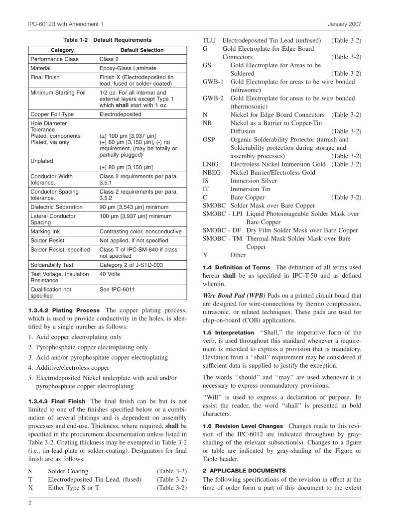
1.3.3.1 Selection (Default) The procurement documen-tation should specify the requirements that can be selectedwithin this specification; however, in the event selectionsare not made in the documentation, Table 1-2 shall apply.
1.3.3.2 Section System (Optional) The following prod-uct selection identifier system is provided for clarificationof the build type.
Quality Specification, the generic quality specification.
Specification, the base performance specification.
Type, the product type per 1.3.2.
Plating Process, the plating process per 1.3.4.2.
Final Finish, the final finish code per 1.3.4.3.
Selective Finish, the selective finish code adder per1.3.4.3, enter ‘‘-’’ when no selective finish is required.
Product Classification, the product classification per 1.3.1or performance specification sheet.
Technology Adder, the technology adder as specified inTable 1-1. Add multiple codes as required.
1.3.4 Material, Plating Process and Final Finish
1.3.4.1 Laminate Material Laminate material is identi-fied by numbers and/or letters, classes and types as speci-fied by the appropriate specification listed in the procure-ment documentation.
Table 1-1 Technology Adder Examples
TechnologyCode Technology
HDI HDI build-up features per IPC-6016
VP Via Protection
WBP Wire Bondable Pads
AMC Active Metal Core
NAMC Nonactive Metal Core
HF External Heat Frame
EP Embedded Passives
VIP-C Via-in-Pad, Conductive Fill
VIP-N Via-in-Pad, Nonconductive FillExample: IPC 6011/6012/3/1/S/-/3/HDI/EP
January 2007 IPC-6012B with Amendment 1
1
1.3.4.2 Plating Process The copper plating process,which is used to provide conductivity in the holes, is iden-tified by a single number as follows:
1. Acid copper electroplating only
2. Pyrophosphate copper electroplating only
3. Acid and/or pyrophosphate copper electroplating
4. Additive/electroless copper
5. Electrodeposited Nickel underplate with acid and/orpyrophosphate copper electroplating
1.3.4.3 Final Finish The final finish can be but is notlimited to one of the finishes specified below or a combi-nation of several platings and is dependent on assemblyprocesses and end-use. Thickness, where required, shall bespecified in the procurement documentation unless listed inTable 3-2. Coating thickness may be exempted in Table 3-2(i.e., tin-lead plate or solder coating). Designators for finalfinish are as follows:
S Solder Coating (Table 3-2)T Electrodeposited Tin-Lead, (fused) (Table 3-2)X Either Type S or T (Table 3-2)
TLU Electrodeposited Tin-Lead (unfused) (Table 3-2)G Gold Electroplate for Edge Board
Connectors (Table 3-2)GS Gold Electroplate for Areas to be
Soldered (Table 3-2)GWB-1 Gold Electroplate for areas to be wire bonded
(ultrasonic)GWB-2 Gold Electroplate for areas to be wire bonded
(thermosonic)N Nickel for Edge Board Connectors (Table 3-2)NB Nickel as a Barrier to Copper-Tin
Diffusion (Table 3-2)OSP Organic Solderability Protector (tarnish and
Solderability protection during storage andassembly processes) (Table 3-2)
ENIG Electroless Nickel Immersion Gold (Table 3-2)NBEG Nickel Barrier/Electroless GoldIS Immersion SilverIT Immersion TinC Bare Copper (Table 3-2)SMOBC Solder Mask over Bare CopperSMOBC - LPI Liquid Photoimageable Solder Mask over
Bare CopperSMOBC - DF Dry Film Solder Mask over Bare CopperSMOBC - TM Thermal Mask Solder Mask over Bare
CopperY Other
1.4 Definition of Terms The definition of all terms usedherein shall be as specified in IPC-T-50 and as definedwherein.
Wire Bond Pad (WPB) Pads on a printed circuit board thatare designed for wire-connections by thermo compression,ultrasonic, or related techniques. These pads are used forchip-on-board (COB) applications.
1.5 Interpretation ‘‘Shall,’’ the imperative form of theverb, is used throughout this standard whenever a require-ment is intended to express a provision that is mandatory.Deviation from a ‘‘shall’’ requirement may be considered ifsufficient data is supplied to justify the exception.
The words ‘‘should’’ and ‘‘may’’ are used whenever it isnecessary to express nonmandatory provisions.
‘‘Will’’ is used to express a declaration of purpose. Toassist the reader, the word ‘‘shall’’ is presented in boldcharacters.
1.6 Revision Level Changes Changes made to this revi-sion of the IPC-6012 are indicated throughout by gray-shading of the relevant subsection(s). Changes to a figureor table are indicated by gray-shading of the Figure orTable header.
2 APPLICABLE DOCUMENTS
The following specifications of the revision in effect at thetime of order form a part of this document to the extent
Table 1-2 Default Requirements
Category Default Selection
Performance Class Class 2
Material Epoxy-Glass Laminate
Final Finish Finish X (Electrodeposited tinlead, fused or solder coated)
Minimum Starting Foil 1/2 oz. For all internal andexternal layers except Type 1which shall start with 1 oz.
Copper Foil Type Electrodeposited
Hole DiameterTolerancePlated, componentsPlated, via only
Unplated
(±) 100 µm [3,937 µin](+) 80 µm [3,150 µin], (-) norequirement, (may be totally orpartially plugged)
(±) 80 µm [3,150 µin]
Conductor Widthtolerance.
Class 2 requirements per para.3.5.1
Conductor Spacingtolerance.
Class 2 requirements per para.3.5.2
Dielectric Separation 90 µm [3,543 µin] minimum
Lateral ConductorSpacing
100 µm [3,937 µin] minimum
Marking Ink Contrasting color, nonconductive
Solder Resist Not applied, if not specified
Solder Resist, specified Class T of IPC-SM-840 if classnot specified
Solderability Test Category 2 of J-STD-003
Test Voltage, InsulationResistance
40 Volts
Qualification notspecified
See IPC-6011
IPC-6012B with Amendment 1 January 2007
2

specified herein. If a conflict of requirements existsbetween IPC-6012 and the listed applicable documents,IPC-6012 shall take precedence.
2.1 IPC1
IPC-A-47 Composite Test Pattern Ten Layer Phototool
IPC-T-50 Terms and Definitions for Interconnecting andPackaging Electronic Circuits
IPC-DD-135 Qualification for Deposited Organic Inter-layer Dielectric Materials for Multichip Modules
IPC-CF-148 Resin Coated Metal for Printed Boards
IPC-CF-152 Composite Material Specifications for PrintedWiring Boards
IPC-D-325 Documentation Requirements for PrintedBoards, Assemblies, and Support Drawings
IPC-A-600 Acceptability of Printed Boards
IPC-TM-650 Test Methods Manual2
2.1.1E 05/04 Microsectioning
2.1.1.2A 05/04 Microsectioning, Semi or AutomaticTechnique Microsection Equipment(Alternate)
2.3.15D 05/04 Purity, Copper Foil or Plating
2.3.25C 02/01 Detection and Measurement of IonizableSurface Contaminants
2.3.38C 05/04 Surface Organic Contaminant DetectionTest
2.3.39C 05/04 Surface Organic Contaminant Identifica-tion Test (Infrared Analytical Method)
2.4.1E 05/04 Adhesion, Tape Testing
2.4.15A 03/76 Surface Finish, Metal Foil
2.4.18.1A 05/04 Tensile Strength and Elongation,In-House Plating
2.4.21E 05/04 Land Bond Strength, Unsupported Com-ponent Hole
2.4.22C 06/99 Bow and Twist
2.4.28.1D 05/04 Adhesion, Solder Resist (Mask), TapeTest Method
2.4.36C 05/04 Rework Simulation, Plated-ThroughHoles for Leaded Components
2.4.41.2A 05/04 Coefficient of Thermal Expansion, StrainGage Method
2.5.5.7A 03/04 Characteristic Impedance and TimeDelay of Lines on Printed Boards byTDR
2.5.7D 05/04 Dielectric Withstand Voltage, PWB
2.6.1F 05/04 Fungus Resistance, Printed WiringMaterials
2.6.3F 05/04 Moisture and Insulation Resistance,Rigid Boards
2.6.4B 05/04 Outgassing, Printed Boards
2.6.5D 05/04 Physical Shock, Multilayer Printed Wir-ing
2.6.7.2B 05/04 Thermal Shock, Continuity and Micro-section, Printed Boards
2.6.8E 05/04 Thermal Stress, Plated-Through Holes
2.6.9B 05/04 Vibration, Rigid Printed Wiring
IPC-QL-653 Certification of Facilities that Inspect/TestPrinted Wiring Boards, Components and Materials
IPC-CC-830 Qualification and Performance of ElectricalInsulating Compound for Printed Board Assemblies
IPC-SM-840 Qualification and Performance of PermanentSolder Mask
IPC-2221 Generic Standard on Printed Board Design
IPC-2251 Design Guide for the Packaging of High SpeedElectronic Circuits
IPC-4101 Specification for Base Materials for Rigid andMultilayer Printed Boards
IPC-4103 Specification for Base Materials for HighSpeed/High Frequency Applications
IPC-4203 Adhesive Coated Dielectric Films for Use asCover Sheets for Flexible Printed Wiring and FlexibleBonding Films
IPC-4552 Electroless Nickel/Immersion Gold Plating forElectronic Interconnections
IPC-4553 Specification for Immersion Silver Plating forPrinted Circuit Boards
IPC-4562 Metal Foil for Printed Wiring Applications
IPC-6011 Generic Performance Specification for PrintedBoards
IPC-6015 Qualification and Performance Specification forOrganic Multichip Module (MCM-L) Mounting and Inter-connecting Structures
IPC-6016 Qualification and Performance Specification forHigh Density Interconnect (HDI) Layers or Boards
IPC-6018 Microwave End Product Board Inspection andTest
1. www.ipc.org2. Current and revised IPC Test Methods are available on the IPC Web site (www.ipc.org/html/testmethods.htm)
January 2007 IPC-6012B with Amendment 1
3

IPC-7711/21A Repair and Rework Guide
IPC-9151 Printed Board Process, Capability, Quality andRelative Reliability (PCQR2) Benchmark Test Standardand Database
IPC-9252 Guidelines and Requirements for ElectricalTesting of Unpopulated Printed Boards
2.2 Joint Industry Standards3
J-STD-003 Solderability Tests for Printed Boards
J-STD-006 Requirements for Electronic Grade SolderAlloys and Fluxed and Non-Fluxed Solid Solders for Elec-tronic Soldering Applications
2.3 Federal4
QQ-S-635 Steel
2.4 Other Publications
2.4.1 American Society for Testing and Materials5
ASTM B-152 Standard Specification for Copper Sheet,Strip, Plate and Rolled Bar
ASTM B-488 Standard Specification for ElectrodepositedCoatings of Gold for Engineering Uses
ASTM B-579 Standard Specification for ElectrodepositedCoating of Tin-Lead Alloy (Solder Plate)
2.4.2 Underwriters Lab6
UL 94 Tests for Flammability of Plastic Materials forParts in Devices and Appliances
2.4.3 National Electrical Manufacturers Association7
NEMA LI-1 Industrial Laminate Thermosetting Product
2.4.4 American Society for Quality8
H0862 Zero Acceptance Number Sampling Plans
2.4.5 AMS9
SAE-AMS-QQ-A-250 Aluminum Alloy, Plate and Sheet
SAE-AMS-QQ-N-290 Nickel Plating (Electrodeposited)
2.4.6 American Society of Mechanical Engineers10
ASME B46.1 Surface Texture (Surface Roughness, Wavi-ness and Lay)
3 REQUIREMENTS
3.1 General Printed boards furnished under this specifi-cation shall meet or exceed the requirements of IPC-6011and the specific performance class as required by the pro-curement documentation. Descriptions and purposes of testcoupons are documented in IPC-2221.
3.2 Materials Used in this Specification
3.2.1 Laminates and Bonding Material for Multilayer
Boards Metal clad laminates, unclad laminates and bond-ing material (prepreg) should be selected from IPC-4101,IPC-4202, IPC-4203, or NEMA LI-1. Polytetrafluoroethyl-ene (PTFE) material types should be selected from IPC-4103. Embedded Passives materials should be as specifiedin the procurement documentation including dielectric,conductive, resistive and insulating characteristics as appli-cable. The specification sheet number, metal cladding typeand metal clad thickness (weight) shall be as specified inthe procurement documentation. When specific require-ments such as the flammability requirements shown in UL94 for laminate and bonding materials are required, it isnecessary to specify those requirements in material pro-curement documents.
3.2.2 External Bonding Materials The material used toadhere external heat sinks or stiffeners to the printed boardshall be selected from IPC-4101, IPC-4203 or as specifiedin the procurement documentation.
3.2.3 Other Dielectric Materials Photoimageable dielec-trics should be selected from IPC-DD-135 and specified inthe procurement documentation. Other dielectric materialsmay be specified in the procurement documentation.
3.2.4 Metal Foils Copper foil shall be in accordancewith IPC-4562. Foil type, foil grade, foil thickness, bondenhancement treatment and foil profile should be specifiedon the master drawing if critical to the function of theprinted board. Resin coated copper foil shall be in accor-dance with IPC-CF-148.
3.2.4.1 Resistive Metal Foil Resistive metal foil shall bespecified in the procurement documentation.
3.2.5 Metal Planes/Cores Metal planes and/or metalcore substrates shall be specified on the master drawing asshown in Table 3-1.
3. www.ipc.org4. www.sae.org5. www.astm.org6. www.ul.com7. www.nema.org8. www.asq.org9. www.sae.org10. www.asme.org
IPC-6012B with Amendment 1 January 2007
4

3.2.6 Metallic Platings and Coatings Thickness of theplating/coating shall be in accordance with Table 3-2. Thecopper plating thickness on the surface, in plated-throughholes, via holes and in blind and buried vias shall be asspecified in Table 3-2. Thickness of platings for a specificuse is shown in Table 3-2. Final finishes selected fromthose listed in 1.3.4.3 or combinations required shallspecify plating thickness except for fused tin-lead platingor solder coating which requires visual coverage andacceptable solderability testing per J-STD-003. Coverageof platings and metallic coatings does not apply to verticalconductor edges; conductor surfaces may have exposedcopper in areas not to be soldered within the limits of3.5.4.7.
Note: The Category of solderability testing shall be speci-fied by the user per J-STD-003; however, in the event it isnot specified the supplier shall test to Category 2 (steamaging is not required).
3.2.6.1 Electroless Depositions and Conductive Coat-ings Electroless depositions and conductive coatingsshall be sufficient for subsequent plating processes andmay be either electroless metal, vacuum deposited metal,or metallic or nonmetallic conductive coatings. Electroless
nickel/immersion gold plating (ENIG) shall be in accor-dance with IPC-4552. Measurement location and extentshall be AABUS.
Caution: Immersion gold thicknesses above 0.125 µm[4.925 µin] can indicate an increased risk of having com-promised the integrity of the nickel undercoat due to exces-sive corrosion. Due to the influence of the design patternand chemistry process variability, acceptance of the solder-ability coupon may not represent the part. Correlation ofthickness measurements across the pattern is stronglyencouraged to demonstrate uniformity of the coating thick-ness.
3.2.6.2 Additive Copper Depositions Additive/electroless copper platings applied as the main conductormetal shall meet the requirements of this specification.
3.2.6.3 Tin-Lead Tin-lead plating shall meet the compo-sition (50-70% tin) requirements of ASTM B-579. Fusingis required unless the unfused option is selected whereinthe thickness specified in Table 3-2 applies.
3.2.6.4 Solder Coating The solder used for solder coat-ing shall be Sn60A, Sn60C, Pb40A, Pb36A, Pb36B,Pb36C, Sn63A, Sn63C or Pb37A per J-STD-006.
3.2.6.5 Nickel Nickel plating shall be in accordancewith SAE-AMS-QQ-N-290 Class 2, except the thicknessshall be in accordance with Table 3-2.
3.2.6.6 Electrodeposited Gold Plating Electrodepositedgold plating shall be in accordance with ASTM-B-488.Purity, hardness and thickness shall be specified in the pro-curement documentation. For Class 3 boards, gold platingshall be Type 1 or 3, Class 1. Gold plating thickness onareas to be wire bonded shall be as specified in Table 3-2.
Table 3-2 Final Finish, Surface Plating and Coating Thickness Requirements
Code Finish Class 1 Class 2 Class 3
S Solder Coating over Bare Copper Coverage & Solderable4 Coverage & Solderable4 Coverage & Solderable4
T Electrodeposited Tin-Lead (fused) -minimum Coverage & Solderable4 Coverage & Solderable4 Coverage & Solderable4
X Either Type S or T As indicated by code
TLU Electrodeposited Tin-Lead Unfused -minimum 8.0 µm [315 µin] 8.0 µm [315 µin] 8.0 µm [315 µin]
G Gold for edge-board connectors andareas not to be soldered - minimum 0.8 µm [31.5 µin] 0.8 µm [31.5 µin] 1.25 µm [49.21 µin]
GS Gold on areas to be soldered -maximum 0.45 µm [17.72 µin] 0.45 µm [17.72 µin] 0.45 µm [17.72 µin]
GWB-1
Gold Electroplate for areas to be wirebonded (ultrasonic) - minimum 0.05 µm [1.97 µin] 0.05 µm [1.97 µin] 0.05 µm [1.97 µin]
Electrolytic nickel under gold for areasto be wire bonded (ultrasonic) -minimum
3 µm [118 µin] 3 µm [118 µin] 3 µm [118 µin]
Table 3-1 Internal or External Metal Planes
Material Specification Alloy
Aluminum SAE-AMS-QQ-A-250 As Specified
Steel QQ-S-635 As Specified
Copper ASTM-B-152 or IPC-4562 As Specified
Copper-Invar-Copper
IPC-CF-152 As Specified
Copper-Moly-Copper
IPC-CF-152 As Specified
Other As Specified As Specified
January 2007 IPC-6012B with Amendment 1
5

Code Finish Class 1 Class 2 Class 3
GWB-2
Gold Electroplate for areas to be wirebonded (thermosonic) - minimum 0.3 µm [11.8 µin] 0.3 µm [11.8 µin] 0.8 µm [31.5 µin]
Electrolytic nickel under gold for areasto be wire bonded (thermosonic) -minimum
3 µm [118 µin] 3 µm [118 µin] 3 µm [118 µin]
N Nickel - Electroplate for Edge BoardConnectors - minimum 2.0 µm [78.7 µin] 2.5 µm [98.4 µin] 2.5 µm [98.4 µin]
NB Nickel - Electroplate as a barrier1 -minimum 1.3 µm [51.2 µin] 1.3 µm [51.2 µin] 1.3 µm [51.2 µin]
OSP Organic Solderability Preservative Solderable4 Solderable4 Solderable4
ENIG
Electroless Nickel - minimum 3 µm [118 µin] 3 µm [118 µin] 3 µm [118 µin]
Immersion Gold (Solderable Surface) Solderable6 Solderable6 Solderable6
Immersion Gold (Other) - minimum 0.05 µm [1.97 µin] 0.05 µm [1.97 µin] 0.05 µm [1.97 µin]
IS Immersion Silver Solderable4,7 Solderable4,7 Solderable4,7
IT Immersion Tin Solderable4 Solderable4 Solderable4
C Bare Copper As indicated in Table 3-7 and/or Table 3-8
Through-Holes
Copper2 - minimum average 20 µm [787 µin] 20 µm [787 µin] 25 µm [984 µin]
Minimum thin areas 18 µm [709 µin] 18 µm [709 µin] 20 µm [787 µin]
Minimum Wrap5 AABUS 5 µm [197 µin] 12 µm [472 µin]
Blind Vias
Copper2
- minimum average 20 µm [787 µin] 20 µm [787 µin] 25 µm [984 µin]
Minimum thin area 18 µm [709 µin] 18 µm [709 µin] 20 µm [787 µin]
Minimum Wrap5 AABUS 5 µm [197 µin] 12 µm [472 µin]
Microvias3 (Blind and Buried)
Copper2 - minimum average 12 µm [472 µin] 12 µm [472 µin] 12 µm [472 µin]
Minimum thin area 10 µm [394 µin] 10 µm [394 µin] 10 µm [394 µin]
Minimum Wrap5 AABUS 5 µm [197 µin] 6 µm [236 µin]
Buried Via Cores
Copper2 - minimum average 13 µm [512 µin] 15 µm [592 µin] 15 µm [592 µin]
Minimum thin area 11 µm [433 µin] 13 µm [512 µin] 13 µm [512 µin]
Minimum Wrap5 AABUS 5 µm [197 µin] 7 µm [276 µin]
Buried Vias (>2 layers)
Copper2 - minimum average 20 µm [787 µin] 20 µm [787 µin] 25 µm [984 µin]
Minimum thin area 18 µm [709 µin] 18 µm [709 µin] 20 µm [787 µin]
Minimum Wrap5 AABUS 5 µm [197 µin] 12 µm [472 µin]1Nickel plating used under the tin-lead or solder coating for high temperature operating environments act as a barrier to prevent the formation of copper-tincompounds.
2Copper plating (1.3.4.2) thickness shall be continuous and wrap from hole walls onto outer surfaces. Refer to IPC-A-600 section on copper plating thicknessfor hole walls.
3Blind microvias are vias that <0.15 mm [0.006 in] in diameter and formed either through laser or mechanical drilling, wet/dry etching, photo imaging orconductive ink-formation followed by a plating operation. All performance characteristics for plated holes, as defined in this document, shall be met. The valuesgiven for blind and buried microvias in Table 3-2 are not applicable for stacked microvias. As of the publication of this specification, there is little known aboutthis structure and the reliability results are not consistent with buried and blind microvias. Stacked microvias may also require different inspection criteria.
4See also 3.3.6.5Wrap copper plating for filled plated holes shall be in accordance with 3.6.2.11.1.6See also 3.2.6.1.7See also 3.2.6.7.
IPC-6012B with Amendment 1 January 2007
6

3.2.6.7 Immersion Silver Plating Immersion silver plat-ing shall be in accordance with IPC-4553. Unlike othersurface finishes, immersion silver plating is available intwo very distinctive but acceptable versions - a thin silverdeposit and a thicker silver deposit. It is imperative that thesupplier of the printed circuit boards inform the user of theimmersion silver plating as to which type of silver they aresupplying. Surface thickness measurements, when requiredfor immersion silver, shall be in accordance with IPC-4553.
NOTE: Pad size for thickness measurements are defined inIPC-4553 and apply for both thin and/or thick silver depos-its. Immersion silver finishes are not recommended for‘‘contact surfaces’’ of Class 3 products.
3.2.6.8 Other Metals and Coatings Other depositionssuch as bare copper, palladium, rhodium, tin, solder alloys,etc., may be used provided they are specified in the pro-curement documentation.
3.2.6.9 Electrodeposited Copper When specified, elec-trodeposited copper platings shall meet the following crite-ria. Frequency of testing shall be determined by the manu-facturer to ensure process control.
a) When tested as specified in IPC-TM-650, Method2.3.15, the purity of copper shall be no less than99.50%.
b) When tested as specified in IPC-TM-650, Method2.4.18.1, with the exception of removing the bake stepin Section 5 within the test method, using 50 µm - 100µm [1,969 µin - 3,937 µin] thick samples, the tensilestrength shall be no less than 36,000 PSI [248 MPa]and the elongation shall be no less than 12%.
3.2.7 Organic Solderability Preservative (OSP) OSPsare anti-tarnish and solderability protectors applied to cop-per to withstand storage and assembly processes in order tomaintain solderability of surfaces. The coating storage, pre-assembly baking and sequential soldering processes impactsolderability. Specific solderability shelf-life and solderingcycle requirements, if applicable, shall be specified in theprocurement documentation.
3.2.8 Polymer Coating (Solder Resist) When permanentsolder resist coating is specified, it shall be a polymer coat-ing conforming to IPC-SM-840. (See 3.7 for solder resistcoverage.)
3.2.9 Fusing Fluids and Fluxes The composition of thefusing fluids and fluxes used in solder coating applicationsshall be capable of cleaning and fusing the tin-lead platingand bare copper to allow for a smooth adherent coating.The fusing fluid shall act as a heat transfer and distributionmedium to prevent damage to the bare laminate of theboard.
Note: Fusing fluid compatibility should be confirmed withend users’ cleanliness requirements due to the diverse inter-actions experienced at assembly soldering.
3.2.10 Marking Inks Marking inks shall be permanent,nonnutrient polymer inks, and shall be specified in theprocurement documentation. Marking inks shall be appliedto the board, or to a label applied to the board. Markinginks and labels must be capable of withstanding fluxes,cleaning solvents, soldering, cleaning and coating pro-cesses encountered in later manufacturing processes. If aconductive marking ink is used, the marking shall betreated as a conductive element on the board.
3.2.11 Hole Fill Insulation Material Electrical insulationmaterial used for hole-fill for metal core printed boardsshall be as specified in the procurement documentation.
3.2.12 Heatsink Planes, External Thickness and materi-als for construction of heatsink planes shall be as specifiedin Table 3-1 and/or the procurement documentation. Bond-ing material shall be as specified in 3.2.2 and/or the pro-curement documentation.
3.2.13 Via Protection Materials for accomplishing viaprotection method shall be as specified in the procurementdocumentation.
3.2.14 Embedded Passive Materials Embedded passivematerials are defined as materials and processes which addcapacitive, resistive and/or inductive functionality withinthe printed circuit board, and which may be used with con-ventional core materials for the manufacture of printed cir-cuit boards. These include laminate materials, resistivemetal foils, plated resistors, conductive pastes, protectantmaterials, etc. Embedded passive materials shall be asspecified in the procurement documentation. At the time ofpublication to the B Revision to the IPC-6012, standardsefforts involving design requirements, material specifica-tion and finished printed board acceptance criteria involv-ing embedded passive technology were underway andintended for future incorporation in IPC-2220 and IPC-6010 series documentation. IPC maintains a listing for theactivities under the D-37 Embedded Passives subcommit-tee at www.ipc.org/committeepage.asp.
3.3 Visual Examination Finished printed boards shall beexamined in accordance with the following procedure.They shall be of uniform quality and shall conform to3.3.1 through 3.3.9.
Visual examination for applicable attributes shall be con-ducted at 3 diopters (approx.1.75X). If confirmation of asuspected defect cannot be made at 3 diopters, it should beverified at progressively higher magnifications (up to 40X)
January 2007 IPC-6012B with Amendment 1
7
to confirm that it is a defect. Dimensional requirementssuch as spacing or conductor width measurements mayrequire other magnifications and devices with reticles orscales in the instrument, which allow accurate measure-ments of the specified dimensions. Contract or specificationmay require other magnifications.
3.3.1 Edges Nicks, crazing or haloing along the edge ofthe board, edge of cutouts and edges of nonplated-throughholes are acceptable provided the penetration does notexceed 50% of the distance from the edge to the nearestconductor or 2.5 mm [0.0984 in], whichever is less. Edgesshall be clean cut and without metallic burrs. Nonmetallicburrs are acceptable as long as they are not loose and/or donot affect fit and function. Panels, which are scored orrouted with a breakaway tab, shall meet the depanelizationrequirements of the assembled board.
3.3.2 Laminate Imperfections Laminate imperfectionsinclude those characteristics that are both internal andexternal within the printed board but are visible from thesurface.
3.3.2.1 Measling Measling is acceptable for Class 1, 2and 3 end product, with the exception of high-voltageapplications as defined by the customer. Refer to IPC-A-600 for more information.
Note: The reader should be aware that, at the time of pub-lication of this amendment to this specification, the IPC-A-610 and IPC-J-STD-001 assembly standards take exceptionto the bare board measling criteria for Class 3 in this speci-fication.
3.3.2.2 Crazing Crazing is acceptable for all classes ofend product provided the imperfection does not reduce theconductor spacing below the minimum and there is nopropagation of the imperfection as a result of thermal test-ing that replicates future assembly processes. For Class 2and 3, the distance of crazing shall not span more than50% of the distance between adjacent conductors. Refer toIPC-A-600 for more information.
3.3.2.3 Delamination/Blister Delamination and blister-ing is acceptable for all classes of end product provided thearea affected by imperfections does not exceed 1% of theboard area on each side and does not reduce the spacingbetween conductive patterns below the minimum conduc-tor spacing. There shall be no propagation of imperfectionsas a result of thermal testing that replicates future assem-bly processes. For Class 2 and 3, the blister or delamina-tion shall not span more than 25% of the distance betweenadjacent conductive patterns. Refer to IPC-A-600 for moreinformation.
3.3.2.4 Foreign Inclusions Translucent particles trappedwithin the board shall be acceptable. Other particles
trapped within the board shall be acceptable, provided theparticle does not reduce the spacing between adjacent con-ductors to below the minimum spacing specified in 3.5.2.
3.3.2.5 Weave Exposure Weave exposure or exposed/disrupted fibers are acceptable for all Classes provided theimperfection does not reduce the remaining conductorspacing (excluding the area(s) with weave exposure) belowthe minimum. Refer to IPC-A-600 for more information.
3.3.2.6 Scratches, Dents, and Tool Marks Scratches,dents, and tool marks are acceptable provided they do notbridge conductors or expose/disrupt fibers greater thanallowed in the paragraphs above and do not reduce thedielectric spacing below the minimum specified.
3.3.2.7 Surface Voids Surface voids are acceptable pro-vided they do not exceed 0.8 mm [0.031 in] in the longestdimension; bridge conductors; or exceed 5% of the totalboard area per side.
3.3.2.8 Color Variations in Bond Enhancement Treat-
ment Mottled appearance or color variation in bondenhancement treatment is acceptable. Random missingareas of treatment shall not exceed 10% of the total con-ductor surface area of the affected layer.
3.3.2.9 Pink Ring No evidence exists that pink ringaffects functionality. The presence of pink ring may beconsidered an indicator of process or design variation butis not a cause for rejection. The focus of concern should bethe quality of the lamination bond.
3.3.3 Plating and Coating Voids in the Hole Plating andcoating voids shall not exceed that allowed by Table 3-3.
3.3.4 Lifted Lands When visually examined in accor-dance with 3.3, there shall be no lifted lands on the deliv-ered (nonstressed) printed circuit board.
3.3.5 Marking Each individual board, each qualificationboard, and quality conformance test circuitry (as opposedto each individual test coupon) shall be marked in order toinsure traceability between the boards/quality conformancetest circuitry and the manufacturing history and to identifythe supplier (logo, etc.). The marking shall be produced bythe same process as used in producing the conductive pat-tern, or by use of a permanent fungistatic ink or paint (see3.2.10), LASER marker or by vibrating pencil marking ona metallic area provided for marking purposes or a perma-nently attached label. Conductive markings, either etchedcopper or conductive ink (see 3.2.10) shall be consideredas electrical elements of the circuit and shall not reducethe electrical spacing requirements. All markings shall becompatible with materials and parts, legible for all tests,
IPC-6012B with Amendment 1 January 2007
8

and in no case affect board performance. Marking shall notcover areas of lands that are to be soldered. Refer to IPC-A-600 for legibility requirements. In addition to this mark-ing, the use of bar code marking is permissible. Whenused, date code shall be formatted per the suppliers discre-tion in order to establish traceability as to when the manu-facturing operations were performed.
3.3.6 Solderability Only those printed boards thatrequire soldering in a subsequent assembly operationrequire solderability testing. Boards that do not require sol-dering do not require solderability testing and this shall bespecified on the master drawing, as in the case where press-fit components are used. Boards to be used only for surfacemount do not require hole solderability testing. Whenrequired by the procurement documentation, acceleratedaging for coating durability shall be in accordance withJ-STD-003. The Category of durability shall be specifiedon the master drawing; however, if not specified, Category2 shall be used. Test coupons or production boards to betested shall be conditioned, if required, and evaluated forsurface and hole solderability using J-STD-003.
When solderability testing is required, consideration shouldbe given to board thickness and copper thickness. As bothincrease, the amount of time to properly wet the sides ofthe holes and the tops of the lands increases proportion-ately.
Note: Accelerated aging (steam aging) is intended for useon coatings of tin/lead, tin/lead solder or tin, but not otherfinal finishes.
3.3.7 Plating Adhesion Printed boards shall be tested inaccordance with IPC-TM-650, Method 2.4.1, using a stripof pressure sensitive tape applied to the surface andremoved by manual force applied perpendicular to the cir-cuit pattern.
There shall be no evidence of any portion of the protectiveplating or the conductor pattern foil being removed, asshown by particles of the plating or pattern foil adhering tothe tape. If overhanging metal (slivers) breaks off andadheres to the tape, it is evidence of overhang or slivers,but not of plating adhesion failure.
3.3.8 Edge Board Contact, Junction of Gold Plate toSolder Finish Exposed copper/plating overlap between
the solder finish and gold plate shall meet the requirementsof Table 3-4. The exposed copper/plating or gold overlapmay exhibit a discolored or gray-black area which isacceptable (see 3.5.4.4).
3.3.9 Workmanship Printed boards shall be processed insuch a manner as to be uniform in quality and show novisual evidence of dirt, foreign matter, oil, fingerprints, tin/lead or solder smear transfer to the dielectric surface, fluxresidue and other contaminants that affect life, ability toassemble and serviceability. Visually dark appearances innonplated holes, which are seen when a metallic or non-metallic semiconductive coating is used, are not foreignmaterial and do not affect life or function. Printed boardsshall be free of defects in excess of those allowed in thisspecification. There shall be no evidence of any lifting orseparation of platings from the surface of the conductivepattern, or of the conductor from the base laminate inexcess of that allowed. There shall be no loose platingslivers on the surface of the printed board.
3.4 Board Dimensional Requirements Inspection ofdimensional requirements shall be as defined herein unlessotherwise agreed upon between user and supplier. Theboard shall meet the dimensional requirements specified inthe procurement documentation. All dimensional character-istics such as, but not limited to, board periphery, thick-ness, cutouts, slots, notches, holes, scoring and edge boardcontacts to connector key area shall be as specified in theprocurement documentation. However, in the event thatdimensional tolerances are not specified in the procurementdocumentation, the applicable feature tolerances of theIPC-2220 design series shall apply. Board dimensionallocations of basic or bilateral tolerance as defined in theprocurement documentation shall be inspected in accor-dance with the applicable AQL classification as specified inTable 4-3.
Automated inspection technology is allowed.
Table 3-3 Plating and Coating Voids Visual Examination
Material Class 1 Class 2 Class 3
Copper1 Three voids allowed per hole in notmore than 10% of the holes.
One void allowed per hole in notmore than 5% of the holes.
None
Finish Coating2 Five voids allowed per hole in notmore than 15% of the holes.
Three voids allowed per hole in notmore than 5% of the holes.
One void allowed per hole in notmore than 5% of the holes.
1 For class 2 product, copper voids shall not exceed 5% of the hole length. For class 1 product, copper voids shall not exceed 10% of the hole length.Circumferential voids shall not extend beyond 90° of the circumference.
2 For class 2 and 3 product, finished coating voids shall not exceed 5% of the hole length. For class 1, finished coating voids shall not exceed 10% of the holelength. Circumferential voids shall not extend beyond 90° for class 1, 2 or 3.
Table 3-4 Edge Board Contact Gap
Max. ExposedCopper Gap Max. Gold Overlap
Class 1 2.5 mm [0.0984 in] 2.5 mm [0.0984 in]
Class 2 1.25 mm [0.04921 in] 1.25 mm [0.04291 in]
Class 3 0.8 mm [0.031 in] 0.8 mm [0.031 in]
January 2007 IPC-6012B with Amendment 1
9

Supplier in-process certification of features of accuracy toreduce inspection is allowed provided the method is docu-mented and demonstrates capability to meet the specifiedrequirements. The supplier may provide a statement of cer-tification of accuracy based on the suppliers sampling planwhich includes a process data collection and recording sys-tem.
In the event that the supplier does not have a process cer-tification system for dimensional accuracy the AQL levelsof Table 4-3 shall apply for each production lot.
3.4.1 Hole Size, Hole Pattern Accuracy and Pattern Fea-
ture Accuracy The hole size tolerance, hole pattern accu-racy and feature location accuracy shall be as specified inthe procurement documentation.
Finished hole size tolerance shall be verified on a samplebasis across all hole sizes applicable to the design. Thenumber of measures per hole size shall be determined bythe manufacturer to adequately sample the quantity ofholes within the population.
Only specific dimensioned holes, to include bothnonplated-through and plated-through, shall be inspectedfor hole pattern accuracy to meet board dimensionalrequirements of 3.4. Unless required by the master draw-ing, hole pattern accuracy for other nonspecifically dimen-sioned holes, such as plated-through holes and vias, neednot be checked as they are database supplied locations andare controlled by annular ring requirements to surface orinternal lands. If required by master drawing, hole pattern
accuracy may be certified by a statement of qualification orby AQL sampling per 3.4.
Pattern feature accuracy shall be as specified in the pro-curement documentation. Pattern feature accuracy may becertified through a statement of qualification or by AQLsampling per 3.4. However, in the event that any of thesecharacteristics are not specified in the procurement docu-mentation, the applicable IPC-2220 design series shallapply. Automated inspection technology is allowed.
Nodules or rough plating in plated-through holes shall notreduce the hole diameter below the minimum limits definedin the procurement document.
3.4.2 Annular Ring and Breakout (External) The mini-mum external annular ring shall meet the requirements ofTable 3-5. The measurement of the annular ring on exter-nal layers is from the inside surface (within the hole) of theplated hole, or unsupported hole, to the outer edge of theannular ring on the surface of the board as shown in Figure3-1. For Class 1 and 2, external plated through holes iden-tified as vias (not having a component) can have up to 90°breakout of the annular ring. The break out shall not occurat the conductor/land intersection and the hole shall meetthe requirements of 3.6.2.1 and 3.6.2.2. The finished boardwith the related breakout shall meet the electrical require-ments of 3.8.2 (see Figures 3-2 and 3-3). Unless prohibitedby the customer, the employment of filleting or ‘‘teardrops’’ to create additional land area at the conductor junc-tion shall be acceptable for Class 1 and 2 and in accor-dance with general requirements for lands with holes
Table 3-5 Minimum Annular Ring
Characteristic Class 1 Class 2 Class 3
ExternalPlated-through
holes
Not greater than 180° breakoutof hole from land when visuallyassessed.1
The land/conductor junction shallnot be reduced below the allow-able width reduction in 3.5.3.1.
Not greater than 90° breakout ofhole from land when visuallyassessed.1
The land/conductor junction shallnot be reduced below the allow-able width reduction in 3.5.3.1. Theconductor junction should never beless than 50 µm [1,969 µin] or theminimum line width, whichever issmaller.
The minimum annular ring shall be50 µm [1,969 µin].
The land/conductor junction shallnot be reduced below the allow-able width reduction in 3.5.3.1.
The minimum external annular ringmay have 20% reduction of theminimum annular ring in isolatedareas due to defects such as pits,dents, nicks, pinholes, or splay inthe annular ring of isolated areas.
InternalPlated-through
holes
Hole breakout is allowed providedthe land/conductor junction is notreduced below the allowable widthreduction in 3.5.3.1.1
90° hole breakout is allowed pro-vided the land/conductor junction isnot reduced below the allowablewidth reduction in 3.5.3.1.1
The minimum internal annular ringshall be 25 µm [984 µin].
ExternalUnsupported
holes
Not greater than 90° breakout ofhole from land when visuallyassessed.1
The land/conductor junction shallnot be reduced below the allow-able width reduction in 3.5.3.1.
Not greater than 90° breakout ofhole from land when visuallyassessed.1
The land/conductor junction shallnot be reduced below the allow-able width reduction in 3.5.3.1.
The minimum annular ring shall be150 µm [5,906 µin].
The minimum external annular ringmay have a 20% reduction of theminimum annular ring in isolatedareas due to defects such as pits,dents, nicks, pinholes or splay inthe annular ring of isolated areas.
1Minimum lateral spacing shall be maintained.Note: (see Figure 3-2 and 3-3 for visual examples of land breakout and conductor width reduction at land).
IPC-6012B with Amendment 1 January 2007
10

detailed in IPC-2221. Employment of filleting or ‘‘teardrops’’ in Class 3 product shall be as agreed upon betweenuser and supplier.
3.4.3 Bow and Twist Unless otherwise specified in theprocurement documentation, when designed in accordancewith 5.2.4 of IPC-2221, the printed board shall have amaximum bow and twist of 0.75% for boards that use sur-face mount components and 1.5% for all other boards. Endproducts shall be assessed in the delivered form.
Bow, twist, or any combination thereof, shall be deter-mined by physical measurement and percentage calculationin accordance with IPC-TM-650, Method 2.4.22.
3.5 Conductor Definition All conductive areas onprinted boards including conductors, lands and planes shallmeet the visual and dimensional requirements of the fol-
lowing sections. The conductor pattern shall be as specifiedin the procurement documentation. Verification of dimen-sional attributes shall be performed in accordance with 3.3and IPC-A-600. AOI inspection methods are allowed.Internal conductors are examined during internal layer pro-cessing prior to multilayer lamination.
3.5.1 Conductor Width and Thickness When not speci-fied on the master drawing the minimum conductor widthshall be 80% of the conductor pattern supplied in the pro-curement documentation. When not specified on the masterdrawing, the minimum conductor thickness shall be inaccordance with 3.6.2.12 and 3.6.2.13.
3.5.2 Conductor Spacing The conductor spacing shallbe within the tolerance specified on the master drawing.Minimum spacing between the conductor and the edge ofthe board shall be as specified on the master drawing.
If minimum spacing is not specified, the allowed reductionin the nominal conductor spacings shown in the engineer-ing documentation due to processing shall be 20% forClass 3 and 30% for Class 1 and 2 (minimum productspacing requirements as previously stated apply).
3.5.3 Conductor Imperfections The conductive patternshall contain no cracks, splits or tears. The physical geom-etry of a conductor is defined by its width x thickness xlength. Any combination of defects specified in 3.5.3.1 and3.5.3.2 shall not reduce the equivalent cross sectional area(width x thickness) of the conductor by more than 20% ofthe minimum value (minimum thickness x minimumwidth) for Class 2 and 3, and 30% of the minimum valuefor Class 1. The total combination of defect area lengths ona conductor shall not be greater than 10% of the conduc-tor length or 25 mm [0.984 in] (for Class 1) or 13 mm[0.512 in] (for Class 2 or 3), whichever is less.
IPC-6012b-3-1
Figure 3-1 Annular Ring Measurement (External)
Measurement ofExternal Annular Ring
IPC-6012b-3-2
Figure 3-2 Breakout of 90° and 180°
B
A
180˚
90˚
A = 1.414 x Radius of PTH
B = Diameter of PTH
IPC-6012b-3-3
Figure 3-3 Conductor Width Reduction
B
A
A = Land/Conductor JunctionB = Minimum Conductor Width
Hole breakout shall not reduce the land/conductor junctionbelow the minimum conductor width. This figure depicts anonconforming condition.
January 2007 IPC-6012B with Amendment 1
11

3.5.3.1 Conductor Width Reduction Allowable reduc-tion of the minimum conductor width (specified or derived)due to misregistration or isolated defects (i.e., edge rough-ness, nicks, pinholes and scratches) which exposes basematerial shall not exceed 20% of the minimum conductorwidth for Class 2 and 3, and 30% of the minimum conduc-tor width for Class 1.
3.5.3.2 Conductor Thickness Reduction Allowablereduction of the minimum conductor thickness due to iso-lated defects (i.e., edge roughness, nicks, pinholes, depres-sions and scratches) shall not exceed 20% of the minimumconductor thickness for Class 2 and 3, and 30% of theminimum conductor thickness for Class 1.
3.5.4 Conductive Surfaces
3.5.4.1 Nicks and Pinholes in Ground or VoltagePlanes Nicks and pinholes are acceptable in ground orvoltage planes for Class 2 and 3 if they do not exceed1.0 mm [0.0394 in] in their longest dimension and there areno more than four per side per 625 cm2 [96.88 in2]. ForClass 1, the longest dimension shall be 1.5 mm [0.0591 in]with no more than six per side, per 625 cm2 [96.88 in2].
3.5.4.2 Solderable Surface Mount Lands Defects alongthe edge of the land or internal to the land shall not exceedthe requirements in 3.5.4.2.1 through 3.5.4.2.2.
3.5.4.2.1 Rectangular Surface Mount Lands Defectssuch as nicks, dents, and pin holes along the external edge
of the land shall not exceed 20% of either the length orwidth of the land for Class 2 or Class 3 boards, or 30% forClass 1, and shall not encroach the pristine area, which isdefined by the central 80% of the land width by 80% of theland length as shown in Figure 3-6. Defects internal to theland shall not exceed 10% of the length or width of theland for Class 2 or Class 3 boards, or 20% for Class 1, andshall remain outside of the pristine area of the surfacemount land. One electrical test probe ‘‘witness’’ mark isallowed within the pristine area for Class 1, 2 and 3.
3.5.4.2.2 Round Surface Mount Lands (BGA Pads)Defects such as nick, dents and pin holes along the edge ofthe land shall not radially extend towards the center of theland by more than 10% of the diameter of the land forClass 1, 2 or 3 boards and shall not extend more than 20%around the circumference of the land for Class 2 or 3boards or 30% for Class 1 as shown in Figure 3-7. Thereshall be no defects within the pristine area which is definedby the central 80% of the land diameter. One electrical testprobe ‘‘witness’’ mark is allowed within the pristine areafor Class 1, 2 and 3.
3.5.4.3 Wire Bond Pads (WBP) The wire bond pad shallhave a final conductor finish as specified in 1.3.4.2 forultrasonic (GWB-1) and thermosonic (GWB-2) wire bond-ing of gold electroplate or electroless nickel/immersiongold (ENIG), or as specified in the procurement documen-tation. The final finish coating thickness shall be per Table3-2 for the applicable coating used. The pristine area shallconsist of the central 80% of the pad width by 80% of thepad length of the wire bond pad as shown in Figure 3-6.The maximum surface roughness in the pristine area of thewire bond pad shall be measured in accordance with anapplicable test method as agreed upon between user andsupplier and shall be 0.8 µm [32 µin] RMS (Root-Mean-Square). If using IPC Method 2.4.15, it is recommendedthat the roughness-width cutoff identified in Method 2.4.15be adjusted to approximately 80% of the maximum lengthof the wire bond pad in order to obtain the RMS valuewithin the pristine area. There shall be no pits, nodules,scratches, electrical test probe ‘‘witness’’ marks, or otherdefects in the pristine area that violate the 0.8 µm [32 µin]RMS roughness requirement. For more information on sur-face roughness, refer to ASME B46.1.
3.5.4.4 Edge Board Connector Lands On gold or othernoble metal plated edge board connector lands, except asnoted below, the insertion or critical contact area shall befree of cuts or scratches that expose underlying nickel orcopper, solder splashes or tin-lead plating, and nodules ormetal bumps that protrude above the surface. Pits, dents ordepressions are acceptable if they do not exceed 0.15 mm[0.00591 in] in their longest dimension and there are notmore than three per land and do not appear on more than
IPC-6012b-3-4
Figure 3-4 Separations at External Foil
OUTER LAYER FOIL
AREA OF ACCEPTABLESEPARATION ALONG THE VERTICAL
EDGE OF THE EXTERNAL FOIL
CONDUCTIVECOATINGS
ELECTROLYTICCOPPER
IPC-6012B with Amendment 1 January 2007
12

30% of the lands. The imperfection limits do not apply toa band 0.15 mm [0.00591 in] wide around the perimeter ofthe land including the critical contact area.
3.5.4.5 Dewetting For tin, tin/lead reflowed, or soldercoated surfaces, dewetting on conductors, areas of solderconnection, and ground or voltage planes is allowed to theextent listed below:
a. Conductors and planes—permitted for all classes.
b. Individual areas of solder connection – Class 1−15%;Class 2−5%; Class 3−5%.
3.5.4.6 Nonwetting For tin, tin/lead reflowed or soldercoated surfaces; nonwetting is not permitted on any con-ductive surface where a solder connection will be required.
3.5.4.7 Final Finish Coverage (Areas not to be soldered)Exposed copper on areas not to be soldered is permitted on1% of the conductor surfaces for Class 3 and 5% of thesurfaces for Class 1 and Class 2. Coverage does not applyto vertical conductor edges.
3.6 Structural Integrity Printed boards shall meet struc-tural integrity requirements for thermally stressed (aftersolder float) evaluation test coupons specified in 3.6.2.
IPC-6012a-3-5
Figure 3-5 Crack Definition
"A" CRACKSCRACK IN
EXTERNAL FOIL
"D" CRACKSCOMPLETEFRACTURE
"B" CRACKS CRACKDOES NOT COMPLETELY
BREAK PLATING (min.plating to remain,
specified in Table 3-2)
"E" CRACKSBARREL CRACK
IN PLATING ONLY
"F" CRACKCORNER CRACKIN PLATING ONLY
"C" CRACKSCRACK IN
INTERNAL FOIL
IPC-6012b-3-6
Figure 3-6 Rectangular Surface Mount Lands
1 Dent/Probe "witness"mark per pad allowed
in pristine area.
≤ 20 % of lengthand width forclass 2 and 3
does notencroach
pristine areaPristine
Area
Equal to central80% of length andwidth of SMT Land
Pin Holesacceptable outside
pristine area.
≤ 10 % length and width for class2 and 3 outside pristine area.
IPC-6012b-3-7
Figure 3-7 Round Surface Mount Lands
Pin Holes acceptableoutside pristine area.
SolderMask
Clearancein Mask
Solderable Ball Land
1 Dent/Probe "witness"mark per pad allowed
in pristine area.
Pristine Area(80% of
Diameter)
Defect ≤10% of landdiameter and ≤20% ofland circumference forclass 2 or 3 and does notencroach pristine area.
January 2007 IPC-6012B with Amendment 1
13
Although the A and B or A/B coupons are assigned for thistest, production boards may be used in lieu of the A and Bor A/B coupons. Areas selected from boards shall containholes and copper features so that all criteria within thisspecification can be evaluated. The production boards andall other test coupons in the quality conformance test cir-cuitry which contain plated-through holes shall be capableof meeting the requirements of this section. Structuralintegrity shall be used to evaluate test coupons or produc-tion boards from Type 2 through Type 6 boards by micro-sectioning techniques. Characteristics not applicable toType 2 boards (i.e., requirements for innerlayer separations,innerlayer inclusions, and inner foil cracks) are not evalu-ated. Dimensional measurements that are only possiblethrough the use of microsectioning techniques are alsodefined in this section. Blind and buried vias shall meet therequirements of plated-through holes. Refer to IPC-2221for appropriate coupon design of blind and buried vias forplated hole evaluation.
The evaluation of all properties and requirements shall beperformed on the thermally stressed test coupon and allrequirements must be met; however, per supplier election,certain properties and conditions as defined in the follow-ing paragraph(s), which are not affected by thermal stress-ing, may be evaluated in a test coupon(s) that has not beenthermally stressed.
a) When a supplier elects to evaluate the unstressed testcoupon for the properties listed in (b), he may do so atany operation following the copper plating operation. Ifthe board undergoes additional thermal excursionsabove the Tg (glass transition temperature) after copperplating, the unstressed test coupon being evaluated shallalso be subjected to these thermal excursions.
b) The properties which are not affected by thermal stressinclude but are not limited to: copper voids, platingfolds/inclusions, burrs and nodules, glass fiber protru-sion, wicking, final coating plating voids, etchback,negative etchback, plating/coating thickness, internaland surface copper layer or foil thickness.
3.6.1 Thermal Stress Testing Test coupons or produc-tion boards shall be thermally stressed in accordance withIPC-TM-650, Method 2.6.8.
Following stress, test coupons or production boards shallbe microsectioned. Microsectioning shall be accomplishedper IPC-TM-650, Method 2.1.1, or 2.1.1.2 on test couponsor production boards. Evaluation of all applicable holesand vias, including blind and buried, for all such structuresfound on the finished printed board shall be inspected inthe vertical cross section in accordance with Table 4-3. Thegrinding and polishing accuracy of the microsection shallbe such that the viewing area of each of the holes is within10% of the drilled diameter of the hole.
Plated-through holes shall be examined for foil and platingintegrity at a magnification of 100X ± 5%. Referee exami-nations shall be accomplished at a magnification of 200X± 5%. Each side of the hole shall be examined indepen-dently. Examination for laminate thickness, foil thickness,plating thickness, lay-up orientation, lamination and platingvoids, and so forth, shall be accomplished at magnifica-tions specified above. For foils less than 3/8 oz., highermagnifications may be required to confirm minimum thick-ness requirement. Plating thicknesses below 1.0 µm[39.4 µin] shall not be measured using metallographictechniques.
Note: When agreed by user and supplier, alternate tech-niques may be used to supplement microsection evaluation.
3.6.2 Requirements for Microsectioned Coupons orProduction Boards When examined in microsection, thetest coupons or production boards shall meet the require-ments of Table 3-6 and paragraph 3.6.2.1 through 3.6.2.17.
3.6.2.1 Plating Integrity Plating integrity in the plated-through holes shall meet the requirements detailed in Table3-6. For Class 2 and 3 product, there shall be no separa-tion of plating layers (except as noted in Table 3-6), noplating cracks, and internal interconnections shall exhibitno separation or contamination between plated hole walland internal layers.
Metal core or thermal planes, when used as electricallyfunctional circuitry, shall meet the above requirementswhen made from copper; but those made from dissimilarmetals may have small spots or pits at their junction withthe hole wall plating. Those areas of contamination orinclusions shall neither exceed 50% of each side of theinterconnection, nor occur in the interface of the coppercladding on the core and the copper plating in the hole wallwhen viewed in the microsection evaluation.
3.6.2.2 Plating Voids Class 1 product shall meet therequirements for plating voids established in Table 3-6. ForClass 2 and 3 product, there shall be no more than onevoid per test coupon or production board, and the follow-ing criteria must be met:
a. There shall be no more than one plating void per testcoupon or production board, regardless of length or size.
b. There shall be no plating void in excess of 5 percent ofthe total printed wiring board thickness.
c. There shall be no plating voids evident at the interfaceof an internal conductive layer and plated hole wall.
d. Circumferential plating voids greater than 90° are notallowed.
Conductor finish plating or coating material between thebase material and copper plating (i.e., behind the hole wallcopper plating) is evidence of a void. Any plated hole
IPC-6012B with Amendment 1 January 2007
14

exhibiting this condition shall be counted as having asingle void for panel acceptance purposes.
If a void is detected during evaluation of a microsectionwhich meets the above criteria, resample in accordancewith Table 4-2 using samples from the same lot to deter-mine if the defect is random. If the additional test couponsor production boards have no plating voids, the productwhich the test coupon or production boards represent areconsidered acceptable; however, if a plating void is presentin the microsections, the product shall be considered non-conforming.
3.6.2.3 Laminate Voids For Class 2 and 3 products,there shall be no laminate voids in Zone B (Figure 3-8) in
excess of 80 µm [3,150 µin]. For Class 1 products, voidsallowed in Zone B (Figure 3-8) shall not exceed 150 µm[5,906 µin]. Multiple voids between two adjacent plated-through holes in the same plane shall not have a combinedlength which exceeds these limits. Voids between twouncommon conductors in either the horizontal or verticaldirection shall not decrease the minimum dielectric spac-ing.
3.6.2.4 Laminate Cracks Laminate cracks in Zone A(Figure 3-8) are acceptable. Cracks that originate in ZoneA and extend into Zone B or are entirely in Zone B shallnot be in excess of 80 µm [3,150 µin] for Class 2 or 3products, and 150 µm [5,906 µin] for Class 1 products.Multiple cracks between two adjacent plated-through holes
Table 3-6 Plated Hole Integrity After Stress
Property Class 1 Class 2 Class 3
Copper voids. Three voids allowed per hole.Voids in the same plane arenot allowed. No void shall
be longer than 5% of boardthickness. No circumferential
voids greater than 90° allowed.
One void allowed per speci-men provided the additional
microsection criteria of3.6.2.2 are met.
One void allowed per speci-men provided the additional
microsection criteria of3.6.2.2 are met.
Plating folds/inclusions2. Must be enclosed. Must be enclosed. Must be enclosed.
Burrs and nodules2. Allowed if minimum holediameter is met.
Allowed if minimum holediameter is met.
Allowed if minimum holediameter is met.
Glass fiber protrusion. Allowed. See 3.6.2.11. Allowed. See 3.6.2.11. Allowed. See 3.6.2.11.
Wicking (Copper Plating). 125 µm [4,921 µin] maximum 100 µm [3,937 µin] maximum 80 µm [3,150 µin] maximum
Innerlayer inclusions (inclu-sions at the interface betweeninternal lands and throughhole plating).
Allowed on only one side ofhole wall at each land locationon 20% of each available land.
None allowed. None allowed.
Internal foil cracks1. ‘‘C’’ cracks allowed on only oneside of hole provided
it does not extendthrough foil thickness.
None allowed. None allowed.
External foil cracks1 (Type‘‘A,’’ ‘‘B’’ and ‘‘D’’ cracks).
‘‘D’’ cracks not allowed. ‘‘A’’and ‘‘B’’ cracks allowed.
‘‘D’’ and ‘‘B’’ cracks notallowed. ‘‘A’’ cracks allowed.
‘‘D’’ and ‘‘B’’ cracks notallowed. ‘‘A’’ cracks allowed.
Barrel/Corner cracks1
(type ‘‘E’’ and ‘‘F’’ cracks).None allowed. None allowed. None allowed.
Innerlayer separation (separa-tion at the interface betweeninternal lands and throughhole plating).
Allowed on only one side ofhole wall at each land locationon 20% of each available land.
None allowed. None allowed.
Separations along the verticaledge of the external land(s).
Allowed (see Figure 3-4) provided it does not extendbeyond the vertical edge of the external copper foil.
Plating separation. Allowed at knee, maximumlength 130 µm [5,118 µin].
None allowed. None allowed.
Hole wall dielectric/platedbarrel separation.
Acceptable provideddimensional and platingrequirements are met.
Acceptable provideddimensional and platingrequirements are met.
Acceptable provideddimensional and platingrequirements are met.
Lifted lands after thermalstress or rework simulation.
Allowed provided the finished boards meet the visual criteria of 3.3.4.
1Copper crack definition: See Figure 3-5‘‘A’’ crack=A crack in the external foil‘‘B’’ crack=A crack that does not completely break plating (minimum plating remains)‘‘C’’ crack=A crack in the internal foil‘‘D’’ crack=A crack in the external foil and plating-complete break in foil and plating‘‘E’’ crack=A barrel crack in plating only‘‘F’’ crack= A corner crack in the plating only2The minimum copper thickness in Table 3-2 must be met.
January 2007 IPC-6012B with Amendment 1
15

in the same plane shall not have a combined length whichexceeds these limits. Cracks between two uncommon con-ductors in either the horizontal or vertical direction shallnot decrease the minimum dielectric spacing.
3.6.2.5 Delamination or Blistering For Class 2 and 3there shall be no evidence of delamination or blistering.For Class 1, if delamination or blistering is present, evalu-ate the entire board per 3.3.2.3.
3.6.2.6 Etchback When specified on the master draw-ing, printed boards shall be etched back for the lateralremoval of resin and/or glass fibers from the drilled holewalls prior to plating. The etchback shall be between 5 µm[197 µin] and 80 µm [3,150 µin] with a preferred depth of13 µm [512 µin]. Shadowing is permitted on one side ofeach land. When no etchback is specified and the boardmanufacturer elects to use etchback, the manufacturer shallbe qualified to perform etchback through demonstration ofqualification test coupons or boards. Caution: Etchbackgreater than 50 µm [1,969 µin] may cause folds or voids inthe plating, which then may not meet the required copperthickness.
3.6.2.7 Smear Removal Smear removal is removal ofresin debris that results from the formation of the hole.Smear removal shall be sufficient to meet the acceptabilitycriteria for plating separation (see Table 3-6). Smearremoval shall not be etched back greater than 25 µm [984µin]; random tears or drill gouges which produce small
areas where the 25 µm [984 µin] depth is exceeded shallnot be evaluated as smear removal. Smear removal is notrequired of Type 1 or Type 2 boards.
3.6.2.8 Negative Etchback Negative etchback shall notexceed the requirements shown in Figure 3-9.
IPC-6012b-3-8
Figure 3-8 Typical Microsection Evaluation Specimen
0.08 mm[0.0031 in] max.
(see Note 1)
Laminateevaluation
area
Plating Voidsin SamePlane
“Zone B” “Zone B”
Laminateevaluation
area
Laminate voids(see Note 2)
Resin recession(see Note 2)
Foil and Platingevaluation area
“Zone A”Thermal zone
0.08 mm[0.0031 in] max.
(see Note 1)
Foil and Platingevaluation area
“Zone A”Thermal zone
0.08 mm[0.0031 in] max.
(see Note 1)
0.08 mm[0.0031 in] max.
(see Note 1)
Void atboundary
line(see Note 2)
Laminatevoid
Foil and Platingevaluation area
“Zone A”Thermal zone
0.08 mm[0.0031 in] max.
longest dimension
Notes:
1. The thermal zone extends 80 µm [0.08 mm] beyond the end of each land, either internal or external, extending furthest into the laminate area.2. Laminate anomalies or imperfections in the Zone A areas are not evaluated on specimens which have been exposed to thermal stress or rework
simulation.3. Delamination/Blistering is evaluated in both Zone A and Zone B.
IPC-6012b-3-9
Figure 3-9 Negative Etchback
Internal Copper Foil
DrilledHoleWall
DistanceZ
DistanceX
Distance "X" shall not exceed:Class 1—25 µm [984 µin]Class 2—25 µm [984 µin]Class 3—13 µm [512 µin]
Distance "Z" shall not exceed:1.5 times the value of Dimension "X"
IPC-6012B with Amendment 1 January 2007
16

3.6.2.9 Annular Ring and Breakout (Internal) Internalannular ring, if not determined by alternate techniques asagreed upon between user and supplier shall be measuredby microsection to verify conformance to Table 3-5 asshown in Figure 3-10. Measurements for internal annularring are from the inside of the drilled hole to the edge ofthe internal land as shown in Figure 3-10. Negative etch-back is evaluated per 3.6.2.8 and Figure 3-9. External padsof sequentially laminated structures are considered as anexternal layer and are evaluated in process prior to addi-tional lamination(s) (see 3.4.2). Microsection analysis isperformed per 3.6.2 (see Figures 3-2 and 3-3). Unless pro-hibited by the customer, the employment of filleting or‘‘tear drops’’ to create additional land area at the conductorjunction shall be acceptable for Class 1 and 2 and in accor-dance with general requirements for lands with holesdetailed in IPC-2221. Employment of filleting or ‘‘teardrops’’ in Class 3 product shall be as agreed upon betweenuser and supplier.
Note: Consideration should be given to how the microsec-tion cut is ‘‘clocked,’’ or rotated. Misregistration can occurrandomly as opposed to orthogonally and therefore anorthogonal cut will not guarantee that a microsection viewwill portray hole breakout, if it exists. See Figures 3-11 and3-12 for an example of how breakout may or may not bedetected within a microsection based on the rotation.
For Class 2 boards, if internal annular ring breakout isdetected in the vertical cross section, but the degree ofbreakout cannot be determined, internal registration may beassessed by nondestructive techniques other than microsec-tion, such as, special patterns, probes, and/or software,which are configured to provide information on the inter-polated annular ring remaining and pattern skew. Tech-niques include, but are not limited to the following:
• The optional F coupon.
• Custom designed electrically testable coupons.
• Radiographic (x-ray) techniques.
• Horizontal microsection.
• CAD/CAM data analysis as correlated to pattern skew bylayer.
Note: Microsectioning or statistical sampling shall be usedto verify correlation of the approved technique, and a cali-bration standard established for the specific techniqueemployed.
3.6.2.9.1 Breakout (Internal) Conditions If misregistra-tion to the point of breakout is detected in vertical micro-sections, the concerns are that:
IPC-6012b-3-10
Figure 3-10 Annular Ring Measurement (Internal)
▼
▼
Measurementof Internal
Annular Ring
IPC-6012b-3-11
Figure 3-11 Microsection Rotations for BreakoutDetection
A-A
A A
B-B
B
C
C-C
M
M-MM
Only a vertical cut at M-M revealsthe minimum conductor width
B
C
IPC-6012b-3-12
Figure 3-12 Comparison of Microsection Rotations
If the mount were cutthrough Section CC, the
microsection wouldlook like this
If the mount were cutthrough Section BB, the
microsection wouldlook like this
If the mount were cutthrough Section AA, the
microsection wouldlook like this
AA
C
A A
B
B
C
Only microsection cut BB revealsthe actual annular ring reduction
CB
CB
January 2007 IPC-6012B with Amendment 1
17

1. The conductor width minimum may be compromised atthe land junction and,
2. There is insufficient electrical spacing.
The extent and direction of misregistration shall be deter-mined.
Actual boards or appropriate test coupons shall then betested to determine compliance. This may be accomplishedby the techniques listed in 3.6.2.9.
3.6.2.10 Lifted Lands Lifted lands are allowed on thethermally stressed microsection.
3.6.2.11 Plating/Coating Thickness Based on microsec-tion examination or on the use of suitable electronic mea-suring equipment, plating/coating thicknesses shall meetthe requirements of Table 3-2, or as specified in the pro-curement document. Measurements in the plated-throughhole shall be reported as an average thickness per side ofthe hole. Isolated thick or thin sections shall not be usedfor averaging. Isolated areas of reduced copper thicknessdue to glass fiber protrusions shall meet the minimumthickness requirements of Table 3-2 as measured from theend of the protrusion to the hole wall.
If copper thickness less than the minimum specified inTable 3-2 is detected in isolated areas, it should be consid-ered a void and resample in accordance with Table 4-2using samples from the same lot to determine if the defectis random. If the additional test coupons or productionboards have no isolated areas of reduced copper thickness,the product which the test coupons or production boardsrepresent are considered acceptable; however, if reducedcopper thickness is present in the microsections, the prod-uct shall be considered nonconforming.
3.6.2.11.1 Copper Wrap Plating Copper wrap platingminimum as specified in Table 3-2 shall be continuousfrom the filled plated hole onto the external surface of anyplated structure and extend by a minimum of 25 µm [984µin] where an annular ring is required (see Figures 3-13and 3-14). Reduction of wrap-plating by processing (sand-ing, etching, planarization, etc.) resulting in insufficientwrap plating is not allowed (see Figure 3-15).
3.6.2.12 Minimum Internal Layer Copper Foil Thick-ness If the internal conductor thickness is specified by afoil weight, the minimum internal copper thickness afterprocessing shall be in accordance with Table 3-7 for allclasses. This table is based on minimum copper foil thick-ness allowances per IPC-4562 followed by two successivescrubbings. Each scrub is expected to remove a specificamount of copper and is represented in the table by a vari-able processing allowance reduction. When the procure-ment documentation specifies a minimum copper thickness
for internal conductors, the conductor shall meet or exceedthat minimum thickness.
3.6.2.13 Minimum Surface Conductor Thickness Theminimum total (copper foil plus copper plating) conductorthickness after processing shall be in accordance withTable 3-8. When the procurement documentation specifies
IPC-6012b-3-13
Figure 3-13 Surface Copper Wrap Measurement(Applicable to all filled plated-through holes)
Minimum Wrap25 µm [984 µin]
Minimum Wrap25 µm [984 µin]
Minimum CopperThickness
VIA
FILL
Note: Cap plating, if required, over filled holesis not considered in wrap copper thicknessmeasurements.
IPC-6012b-3-14
Figure 3-14 Wrap Copper in Type 4 PCB (Acceptable)
VIA
FILL
VIA
FILL
IPC-6012b-3-15
Figure 3-15 Wrap Copper Removed by ExcessiveSanding/Planarization (Not Acceptable)
VIA
FILL
VIA
FILL
Note: Dimension lines and arrows indicate where wrap copper hasbeen removed.
IPC-6012B with Amendment 1 January 2007
18

a minimum copper thickness for external conductors, thetest coupon or production board shall meet or exceed thatminimum thickness. The minimum surface conductorthickness after processing values given in Table 3-8 aredetermined by the following equation:
Minimum Surface Conductor Thickness = a + b - c
Where:
a = Absolute copper foil minimum (IPC-4562 nominal less10% reduction).
b = Minimum copper plating thickness (20 µm [787 µin]for Class 1 and 2; 25 µm [984 µin] for Class 3).
c = A maximum variable processing allowance reduction.
3.6.2.14 Metal Cores The minimum lateral spacingbetween adjacent conductive surfaces, nonfunctional landsand/or plated-through holes, and the metal plane shall be100 µm [3,937 µin] (see Figure 3-16).
3.6.2.15 Dielectric Thickness The minimum dielectricspacing shall be specified in the procurement documenta-
Table 3-7 Internal Layer Foil Thickness after Processing
WeightAbsolute Cu Min. (IPC-4562
less 10% reduction) (µm) [µin]Maximum Variable Processing
Allowance Reduction* (µm) [µin]Minimum Final Finish
after Processing (µm) [µin]
1/8 oz. [5.10] 4.60 [181] 1.50 [59] 3.1 [122]
1/4 oz. [8.50] 7.70 [303] 1.50 [59] 6.2 [244]
3/8 oz. [12.00] 10.80 [425] 1.50 [59] 9.3 [366]
1/2 oz. [17.10] 15.40 [606] 4.00 [157] 11.4 [449]
1 oz. [34.30] 30.90 [1,217] 6.00 [236] 24.9 [980]
2 oz. [68.60] 61.70 [2,429] 6.00 [236] 55.7 [2,193]
3 oz. [102.90] 92.60 [3,646] 6.00 [236] 86.6 [3,409]
4 oz. [137.20] 123.50 [4,862] 6.00 [236] 117.5 [4,626]
Above 4 oz.[137.20]
IPC-4562 valueless 10% reduction
6.00 [236] 6 µm [236 µin] below minimum thickness of calcu-lated 10% reduction of foil thickness in IPC-4562
* Process allowance reduction does not allow for rework processes for weights below 1/2 oz. For 1/2 oz. and above, the process allowance reduction allows forone rework process.
Table 3-8 External Conductor Thickness after Plating
Weight1
Absolute Cu Min.(IPC-4562 less10% reduction)
(µm) [µin]
Plus minimumplating for
Class 1 and 2(20 µm) [787 µin]2
Plus minimumplating for
Class 3(25 µm) [984 µin]2
Maximum VariableProcessing AllowanceReduction3 (µm) [µin]
Minimum SurfaceConductor Thickness after
Processing (µm) [µin]
Class 1 & 2 Class 3
1/8 oz. 4.60 [181] 24.60 [967] 29.60 [1,165] 1.50 [59] 23.1 [909] 28.1 [1,106]
1/4 oz. 7.70 [303] 27.70 [1,091] 32.70 [1,287] 1.50 [59] 26.2 [1,031] 31.2 [1,228]
3/8 oz. 10.80 [425] 30.80 [1,213] 35.80 [1,409] 1.50 [59] 29.3 [1,154] 34.3 [1,350]
1/2 oz. 15.40 [606] 35.40 [1,394] 40.40 [1,591] 2.00 [79] 33.4 [1,315] 38.4 [1,512]
1 oz. 30.90 [1,217] 50.90 [2,004] 55.90 [2,201] 3.00 [118] 47.9 [1,886] 52.9 [2,083]
2 oz. 61.70 [2,429] 81.70 [3,217] 86.70 [3,413] 3.00 [118] 78.7 [3,098] 83.7 [3,295]
3 oz. 92.60 [3,646] 112.60 [4,433] 117.60 [4,630] 4.00 [157] 108.6 [4,276] 113.6 [4,472]
4 oz. 123.50 [4,862] 143.50 [5,650] 148.50 [5,846] 4.00 [157] 139.5 [5,492] 144.5 [5,689]1. Starting foil weight of design requirement per procurement documentation.2. Process allowance reduction does not allow for rework processes for weights below 1/2 oz. For 1/2 oz. and above, the process allowance reduction allows for
one rework process.3. Reference: Min. Cu Plating Thickness
Class 1 = 20 µm [787 µin] Class 2 = 20 µm [787 µin] Class 3 = 25 µm [984 µin]
IPC-6012b-3-16
Figure 3-16 Metal Core to Plated-Through Hole Spacing
Core
Min. MetalCore Spacing
▼ ▼▼▼
January 2007 IPC-6012B with Amendment 1
19

tion. Figure 3-17 provides an example of a measurementtechnique for minimum dielectric spacing.
Note: Minimum dielectric spacing may be specified to be30 µm [1,181 µin]; however, low profile copper foilsshould be used and the voltages employed should be takeninto consideration so as not to cause breakdown betweenlayers. If the minimum dielectric spacing and the numberof reinforcing layers are not specified, the minimum dielec-tric spacing is 90 µm [3,543 µin] and the number of rein-forcing layers may be selected by the supplier. When thenominal dielectric thickness on the drawing is less than90 µm [3,543 µin], the minimum dielectric spacing is25 µm [984 µin] and the number of reinforcing layers maybe selected by the supplier.
3.6.2.16 Material Fill of Blind and Buried Vias Fillrequirements for blind vias shall be as specified in the pro-curement documentation. Buried vias shall be at least 60%filled with the laminating resin or similar via filling mate-rial for Class 2 and Class 3. They may be completely voidof fill material for Class 1.
3.6.2.17 Nail Heading No evidence exists that nail head-ing affects functionality. The presence of nail heading maybe considered an indicator of process or design variationbut is not a cause for rejection.
3.7 Solder Resist (Solder Mask) Requirements Whensolder resist is required on printed boards, it shall meet thequalification/conformance requirements of IPC-SM-840. Ifa solder resist performance class is not specified for Class1 or 2, IPC-SM-840 Class T shall be used. For Class 3board performance, IPC-SM-840 Class H shall be used.The following other conformance requirements apply:
3.7.1 Solder Resist Coverage Solder resist coveragemanufacturing variations resulting in skips, voids, and mis-registration are subject to the following restrictions:
a. Metal conductors shall not be exposed in areas wheresolder resist is required. Touch up, if required to cover
these areas with solder resist, shall be of a material thatis compatible to and of equal resistance to soldering andcleaning as the originally applied solder resist.
b. In areas containing parallel conductors, solder resistvariations shall not expose adjacent conductors unlessthe area between the conductors is purposely left blankas for a test point or for some surface mount devices.
c. Conductors under components shall not be exposed orshall be otherwise electrically isolated. If the compo-nent pattern is not readily apparent, the area covered bya component shall be shown in the procurement docu-ment.
d. Solder resist need not be flush with the surface of theland. Misregistration of a solder resist defined featureshall not expose adjacent isolated lands or conductors.
e. Solder resist is allowed on lands for plated-throughholes to which solder connections are to be made pro-vided the external annular ring requirements for thatClass of products are not violated; resist shall notencroach upon the barrel of this type of plated-throughhole. Other surfaces such as edge board connector fin-gers and surface mount lands shall be free of solderresist except as specified. Solder resist is allowed inplated-through holes and via holes into which no com-ponent lead is soldered unless the procurement docu-ment requires that the holes be completely solder filled.Solder resist may tent or plug via holes and may berequired for that purpose. Test points that are intendedfor assembly testing must be free of solder resist unlesscoverage is specified.
f. When a land contains no plated-through holes, as in thecase of surface mount or ball grid array lands, misregis-tration shall not cause encroachment of the solder resiston the land or lack of solder-resist-definition in excessof the following:
1) on surface mount lands misregistration shall notcause encroachment of the solder resist over the landarea greater than 50 µm [1,969 µin] for a pitch of1.25 mm [0.04921 in] or greater; and encroachmentshall not exceed 25 µm [984 µin] for a pitch lessthan 1.25 mm [0.04921 in]; encroachment mayoccur on adjacent sides but not on opposite sides ofa surface mount land.
2) on ball grid array lands, if the land is solder-resist-defined, misregistration may allow a 90° breakout ofthe solder resist on the land; if clearance is specified,no encroachment of the solder resist on the land isallowed except at the conductor attachment.
g. Pits and voids are allowed in nonconductor areas pro-vided they have adherent edges and do not exhibit lift-ing or blistering in excess of allowance in 3.7.2.
h. Coverage between closely spaced surface mount landsshall be as required by procurement documentation.
IPC-6012b-3-17
Figure 3-17 Measurement of Minimum Dielectric Spacing
MinimumDielectricThickness
IPC-6012B with Amendment 1 January 2007
20

i. When design requires coverage to the board edge, chip-ping or lifting of solder resist along the board edge afterfabrication shall not penetrate more than 1.25 mm[0.04921 in] or 50% of the distance to the closest con-ductor, whichever is less.
3.7.2 Solder Resist Cure and Adhesion The cured sol-der mask coating shall not exhibit tackiness, delamination,bubbles or blistering to the following extent:
• Class 1 does not bridge between conductors.
• Class 2 and 3 two per side, maximum size 0.25 mm[0.00984 in] in longest dimension, does not reduce elec-trical spacing between conductors by more than 25%.
Rework and touch up, if required to cover these areas withsolder resist, shall be of a material that is compatible toand of equal resistance to soldering and cleaning as theoriginally applied solder resist. When tested in accordancewith IPC-TM-650, Method 2.4.28.1, the maximum percent-age of cured solder resist lifting from the G coupon shallbe in accordance with Table 3-9.
3.7.3 Solder Resist Thickness Solder resist thickness isnot measured unless specified in the procurement docu-ments. If a thickness measurement is required, instrumen-tal methods may be used or assessment may be made usinga microsection of the parallel conductors on the E coupon.
3.8 Electrical Requirements When tested as specified inTable 4-3 and Table 4-4, the printed boards shall meet theelectrical requirements detailed in the following para-graphs.
3.8.1 Dielectric Withstanding Voltage Applicable testcoupons or production boards shall meet the requirementsof Table 3-10, without flashover, or breakdown betweenconductors, or conductors and lands. The dielectric with-standing voltage test shall be performed in accordance withIPC-TM-650, Method 2.5.7. The dielectric withstandingvoltage shall be applied between all common portions ofeach conductor pattern and adjacent common portions ofeach conductor pattern. The voltage shall be appliedbetween conductor patterns of each layer and the electri-cally isolated pattern of each adjacent layer.
3.8.2 Electrical Continuity and Insulation ResistanceBoards shall be tested in accordance with IPC-9252.
3.8.2.1 Continuity Printed boards and qualification testboards shall be tested in accordance with the procedureoutlined below. There shall be no circuits whose resistanceexceeds the values established in the procurement docu-mentation. Specialized circuitry consisting of long runs ofvery narrow conductors, or short runs of very large conduc-tors may increase or decrease these values. The acceptabil-ity criteria for these specialized conductors must be speci-fied in the procurement documentation.
A current shall be passed through each conductor or groupof interconnected conductors by applying electrodes on theterminals at each end of the conductor or group of conduc-tors. The current passed through the conductors shall notexceed that specified in IPC-2221 for the smallest conduc-tor in the circuit. For qualification as referenced in 4.1.1and 4.1.2, the test current shall not exceed one ampere.Boards with designed resistive patterns shall meet theresistance requirements specified on the master drawing.
3.8.2.2 Insulation Resistance Printed Boards or qualifi-cation test boards shall be tested in accordance with thefollowing procedure. The insulation resistance betweenconductors shall meet the values established in the pro-curement documentation.
The voltage applied between networks must be highenough to provide sufficient current resolution for the mea-surement. At the same time, it must be low enough to pre-vent arc-over between adjacent networks, which couldinduce defects within the product. For manual testing, thevoltage shall be 200 volts minimum and shall be appliedfor a minimum of five seconds. When automated testequipment is used, the minimum applied test voltage shallbe the maximum rated voltage of the board. When notspecified, use the default value in Table 1-2.
3.8.3 Circuit/Plated-Through Shorts to Metal Sub-strate Printed boards shall be tested in accordance with3.8.1 except that polarizing voltage of 500 volts (DC) shallbe applied between conductors and/or lands and the metal-lic heatsink in a manner such that each conductor/land areais tested (e.g., using a metallic brush or aluminum foil).
The board shall be capable of withstanding 500 volts (DC)between circuitry/plated-through holes and the metal coresubstrates. There shall be no flashover or dielectric break-down.
Table 3-9 Solder Resist Adhesion
Surface
Maximum Percentage Loss Allowed
Class 1 Class 2 Class 3
Bare Copper 10 5 0
Gold or Nickel 25 10 5
Base Laminate 10 5 0
Melting Metals(Tin-lead plating,fused tin-lead, andbright acid- tin)
50 25 10
Table 3-10 Dielectric Withstanding Voltages
Class 1 Class 2 and 3
VoltageFor Spacing 80 µm[3,150 µin] or greater
No requirement 500 Vdc +15, -0
VoltageFor Spacing less than80 µm [3,150 µin]
No requirement 250 Vdc +15, -0
Time No requirement 30 sec +3, -0
January 2007 IPC-6012B with Amendment 1
21

3.8.4 Moisture and Insulation Resistance (MIR) Testcoupons shall be tested in accordance with the procedureoutlined below. The test coupon shall not exhibit subsur-face imperfections in excess of that allowed in 3.3.2. Insu-lation resistance shall meet the minimum requirementsshown in Table 3-11 (at 500 volts DC). Noncomponentflush boards shall have a minimum requirement of 50 Mfor all classes. Insulation resistance requirements in theas-received condition are detailed in special requirementsection (see 3.10.9).
The moisture and insulation resistance for printed boardsshall be performed in accordance with IPC-TM-650,Method 2.6.3. Conformal coating in accordance with IPC-CC-830 shall be applied to the external conductors prior tochamber exposure. Final measurements shall be made atroom temperature within two hours after removal from thetest chamber. All layers have a 100 ± 10 volts DC polariz-ing voltage applied during chamber exposure. Mealing ofthe conformal coating shall not extend more than 3 mm[0.12 in] from the edge of the test coupon or productionboard.
3.8.4.1 Dielectric Withstanding Voltage After MIR Adielectric withstanding voltage test shall be performed aftermoisture and insulation resistance in accordance with 3.8.1.
3.9 Cleanliness Printed boards shall be tested in accor-dance with IPC-TM-650, Method 2.3.25 paragraph 4Resistance of Solvent Extract Method. Equivalent methodsmay be used in lieu of the method specified; however itshall be demonstrated to have equal or better sensitivityand employ solvents with the ability to dissolve flux resi-due or other contaminants as does the solution presentlyspecified.
3.9.1 Cleanliness Prior to Solder Resist ApplicationWhen a printed board requires a permanent solder resistcoating, the uncoated boards shall be within the allowablelimits of ionic and other contaminants prior to the applica-tion of solder resist coating. When noncoated printedboards are tested per 3.9, the contamination level shall notbe greater than an equivalent of 1.56 µg/cm2 of sodiumchloride.
3.9.2 Cleanliness After Solder Resist, Solder, or Alter-native Surface Coating Application When specified,printed boards shall be tested per 3.9 and meet the require-ments in the procurement documentation.
3.9.3 Cleanliness of Inner Layers After Oxide TreatmentPrior to Lamination When specified, inner layers shall betested per 3.9 and meet the requirements of the procure-ment documentation.
3.10 Special Requirements When specified in the pro-curement documentation, some or all of the special require-ments listed in this section (3.10) shall apply. A notation inthe procurement documentation will designate which arerequired.
3.10.1 Outgassing The degree of outgassing shall havea Total Mass Loss (TML) of less than one percent (1%)and Collectible Volatile Condensable Material (CVCM) ofless than one tenth of one percent (0.1%). Mass loss shallbe determined on test coupons or production boards of rep-resentative substrates when tested in accordance with IPC-TM-650, Method 2.6.4.
3.10.2 Organic Contamination Noncoated printedboards shall be tested in accordance with the procedureoutlined below. Any visual evidence of organic residueshall constitute a failure.
The printed board shall be tested in accordance with IPC-TM-650, Methods 2.3.38 or 2.3.39. The first is a qualitativemethod in which very pure acetonitrile is dripped acrossthe test coupon or production board and collected on amicroscope slide. It is dried and compared with a slidehaving dried, uncontaminated acetonitrile on it for visualevidence of organic residue. If evidence of organic con-tamination is detected by this test, Method 2.3.39 is used todetermine the nature of the contaminant by the use of infra-red spectrophotometric analysis using the Multiple InternalReflectance (MIR) method.
3.10.3 Fungus Resistance Completed boards or repre-sentative board sections from the lot shall not support fun-gus growth when tested as follows: The specimen(s) shallbe tested in accordance with IPC-TM-650, Method 2.6.1.
3.10.4 Vibration The test coupon or production boardshall pass the circuitry test in 3.8.2 following the vibrationtest procedure below and shall not exhibit bow or twist inexcess of that allowed in 3.4.4 following testing.
The boards shall be subjected to both a cycling and reso-nance dwell test with the flat surface of the board mountedperpendicular to the axis of vibration in accordance withIPC-TM-650, Method 2.6.9.
Cycling Test – The cycling test shall consist of one sweepfrom 20 to 2000 Hz performed in 16 minutes. Input accel-eration over the 20 to 2000 Hz frequency range shall bemaintained to 15 Gs.
Resonance Dwell – Test coupons or production boardsshall be subjected to a 30 minute resonance dwell with 25
Table 3-11 Insulation Resistance
Class 1 Class 2 Class 3
As received Maintainelectricalfunction
500 MΩ 500 MΩ
After exposureto moisture
Maintainelectricalfunction
100 MΩ 500 MΩ
IPC-6012B with Amendment 1 January 2007
22

Gs input or a maximum of 100 Gs output measured at thegeometric center of the test coupon or production board.The test coupons or production boards shall be restrainedfrom movement by fixturing on all four sides.
3.10.5 Mechanical Shock The test boards shall pass thecircuitry test in 3.8.2 after being subjected to mechanicalshock testing as follows.
The mechanical shock test shall be performed in accor-dance with IPC-TM-650, Method 2.6.5. The boards shallbe subjected three times to a shock pulse of 100 Gs with aduration of 6.5 milliseconds in each of the three principalplanes. The test coupons or production boards shall berestrained from movement by fixturing on all four edges.
3.10.6 Impedance Testing Requirements for impedanceshall be specified on the master drawing. Impedance test-ing may be performed on a test coupon or a designated cir-cuit in the production board. Time Domain Reflectometers(TDR) are used for electrical testing, but for large imped-ance tolerances, mechanical measurements from a micro-section utilizing a special test coupon can be used to calcu-late and verify impedance values. (See IPC-2251 for theequations for calculating impedance from the test couponand IPC-TM-650, Method 2.5.5.7, for the test methodusing the TDR technique.)
3.10.7 Coefficient of Thermal Expansion (CTE) Whenboards that have metal cores or reinforcements with arequirement to constrain the thermal expansion in the pla-nar directions, the Coefficient of Thermal Expansion shallbe within ± 2 ppm/°C for the CTE and temperature rangespecified on the procurement documentation. Testing shallbe by the strain gauge method in accordance with IPC-TM-650, Method 2.4.41.2. If agreed upon by user and supplier,other methods of determining the CTE may be used.
3.10.8 Thermal Shock When specified, printed boards ortest coupons shall be tested in accordance with IPC-TM-650, Method 2.6.7.2. An increase in resistance of 10% ormore shall be considered a reject. After microsectioning,the boards or test coupons shall meet the requirements ofTable 3-6 and Figure 3-5.
3.10.9 Surface Insulation Resistance (As Received)Test coupons shall be tested in accordance with the proce-dure outlined below. The insulation resistance shall be noless than that shown in Table 3-11.
Test coupons or production boards should be conditioned at50 ± 5 °C [122 ± 9 °F] with no added humidity for a periodof 24 hours. After cooling, the insulation resistance testshall be performed in accordance with the ambient tem-perature measurements specified in IPC-TM-650, Method2.6.3.
3.10.10 Metal Core (Horizontal Microsection) Whenspecified, metal core printed boards which have clearancebetween the plated-through holes and the metal core shallrequire a horizontal microsection prepared to view themetal core/hole fill insulation. Test coupons or productionboards shall have been subjected to thermal stress in accor-dance with 3.6.1 prior to microsectioning. Wicking, radialcracks, lateral spacing or voids in the hole-fill insulationmaterial shall not reduce the electrical spacing betweenadjacent conductive surfaces to less than 100 µm [3,937µin]. Wicking and/or radial cracks shall not exceed 75 µm[2,953 µin] from the plated-through hole edge into thehole-fill.
3.10.11 Rework Simulation
3.10.11.1 Through Hole Components When specified,printed boards or test coupons shall be tested in accordancewith IPC-TM-650, Method 2.4.36 and then microsectionedand examined in accordance with 3.6. Lifted lands areallowed.
3.10.11.2 Surface Mount Components When specified,100% surface mount boards shall be tested in accordancewith the procurement documentation.
3.10.12 Bond Strength, Unsupported Component HoleLand The unsupported component hole lands shall betested in accordance with IPC-TM-650, Method 2.4.21.The unsupported component hole land shall withstand 2 kgor 35 kg/cm2, whichever is less.
Calculations of land area of the unsupported hole do notinclude the area occupied by the hole.
3.11 Repair Repair of bare boards shall be as agreedupon between the user and supplier for each set of procure-ment documentation (see IPC-7711/21A).
3.11.1 Circuit Repairs When agreed on between userand supplier, circuit repairs on Classes 1, 2, and 3 will bepermitted. As a guideline, there should be no more thantwo circuit repairs for each 0.09 m2 or less of layer area perside. Circuit repairs on any impedance controlled circuitsshall not violate the impedance requirement and shall havethe agreement of the user. Circuit repairs shall not violatethe minimum electrical spacing requirements.
3.12 Rework Rework is permitted for all Classes. Thetouch-up of surface imperfections in the base material orremoval of residual plating materials or extraneous copperwill be permitted for all products when such action doesnot affect the functional integrity of the board.
4 QUALITY ASSURANCE PROVISIONS
4.1 General General Quality Assurance Provisions arespecified in IPC-6011 and each sectional specification. The
January 2007 IPC-6012B with Amendment 1
23

requirements specific to Rigid Boards are contained in thisspecification and include the Qualification Testing, Accep-tance Testing and Frequency of Quality Conformance Test-ing.
4.1.1 Qualification Qualification is agreed upon by theuser and supplier (see IPC-6011). The qualification shouldconsist of capability analysis assessments (see IPC-9151),preproduction samples, production sample or test coupons(see IPC-6011) that are produced by the same equipmentand procedures planned for the production boards. Qualifi-cation should include those applicable tests as referenced inTables 4-3 and 4-4. Qualification as agreed by the user mayconsist of documentation that supplier has furnished simi-lar product to other users or to other similar specifications.
4.1.2 Sample Test Coupons Sample test coupons maybe used for qualification or for on-going process control.Master drawings, databases, or phototools are availablefrom IPC. For each type (see 1.3.2) the master drawing andphototool is listed as follows:
Type 1 Use surface layers of IPC-A-47Type 2 Use surface layers of IPC-A-47Type 3 Use Master Drawing IPC-100103
within IPC-A-47
Note: IPC-100002 is the universal drilling and profile mas-ter drawing. Both the IPC-100103 and IPC-100002 are partof the IPC-A-47 phototool artwork package.
Table 4-1 specifies the test coupons on the sample used forqualification and process capability evaluations. Thenumerical designation following each coupon, such as M5,relates to multiple instances of the coupon on the sample asindicated within IPC-A-47.
4.2 Acceptance Tests Use the C=0 Zero AcceptanceNumber Sampling Plan specified in Table 4-2 when
‘‘Sample’’ is indicated in Table 4-3. Acceptance testingshall be performed as specified in Table 4-3 to the require-ments of this specification and IPC-6011 using either testcoupons and/or production boards. The test coupons aredescribed in IPC-2221, which indicates the purpose of eachcoupon and its frequency on a manufacturing panel.
4.2.1 C=0 Zero Acceptance Number Sampling PlanThe C=0 Zero Acceptance Number Sampling Plan providesgreater or equal protection for the Lot Tolerance PercentDefective (L.T.P.D.) protection at the 0.10 ‘‘consumerrisk’’ level. The Index Values at the top of each sample sizecolumn associates to the A.Q.L. level. For a lot to beaccepted, all samples (shown in Table 4-2) shall conformto the requirements. Disposition of rejected lots shall befully documented. Contact the American Society for Qual-ity Control for more information on sampling plans(H0862).
4.2.2 Referee Tests Two additional microsection setsfrom the same panel may be prepared and evaluated formicrosection defects that are considered to be isolated orrandom in nature or caused by microsection preparation.For acceptance, both referee sets must be defect free.
4.3 Quality Conformance Testing Quality ConformanceTesting shall consist of inspections specified in Table 4-4in a laboratory, which meets all requirements of IPC-QL-653, unless otherwise specified by the user. Class 3 testingmay be extended to reliability test and evaluation for Class2.
4.3.1 Coupon Selection Two sets of test coupons of themost complex pattern of each type of material processedduring the inspection period shall be selected from lots thathave passed acceptance testing.
IPC-6012B with Amendment 1 January 2007
24

Table 4-1 Qualification Test Coupons
Test Type 1 Types 2,3,5 Types 4, 6 Board
Visual (1) All All All X
SolderabilitySurface (1)Hole (1)
M2, M5S1, S6 S1, S6
Dimensional (1) All All All X
PhysicalPlating Adhesion (1)Bond Strength
N1, N4, N5A2, A3, A6
N1, N4, N5 N1, N4, N5
Construction IntegrityPTH Prior to StressAdditional Dimensions
A1, A4, A5A1, A4, A5
Design Req.Design Req.
PTH After StressThermal StressHorizontal micro (Metal Core)Rework Simulation
A1, A4, A5B1, B4, B5B2, B3, B6
Design Req.A1, B4, B5
Design Req.
Electrical RequirementsDWVContinuityInsulation Resistance
E1, E4, E5D1, D4, D5E2, E3, E6
E1, E4, E5D1, D4, D5E2, E3, E6
E1, E4, E5Design Req.E2, E3, E6
EnvironmentalThermal ShockCleanliness (1)Moisture/Insulation Resistance
D2, D3, D6
E1, E4, E5
D2, D3, D6
E1, E4, E5
Design Req.
E1, E4, E5X
Special Requirements (2)OutgassingOrganic ContaminationFungusVibrationMechanical ShockImpedanceThermal Expansion
H1, H2, H3
XXXX
Note 1 – Not technology dependent.Note 2 – Additional test coupons required, to be agreed upon between user and manufacturer.
Table 4-2 C=0 Sampling Plan (Sample Size for Specific Index Value*)
Lot Size
Class 1 Class 2 Class 3
2.5* 4.0* 6.5* 1.5* 2.5* 4.0* 0.10* 1.0* 2.5* 4.0*
1-8 5 3 2 ** 5 3 ** ** 5 3
9-15 5 3 2 8 5 3 ** 13 5 3
16-25 5 3 3 8 5 3 ** 13 5 3
26-50 5 5 5 8 5 5 ** 13 5 5
51-90 7 6 5 8 7 6 ** 13 7 6
91-150 11 7 6 12 11 7 125 13 11 7
151-280 13 10 7 19 13 10 125 20 13 10
281-500 16 11 9 21 16 11 125 29 16 11
501-1200 19 15 11 27 19 15 125 34 19 15
1201-3200 23 18 13 35 23 18 125 42 23 18
3201-10,000 29 22 15 38 29 22 192 50 29 22
10,001-35,000 35 29 15 46 35 29 294 60 35 29*Index Value is associated to the A.Q.L. value. If a particular product is determined to be ‘‘critical’’ by the user and a smaller index value is required, the usershall designate the requirement in the procurement document and should state the ‘‘critical’’ requirement on the master drawing.
**Denotes inspect entire lot.
January 2007 IPC-6012B with Amendment 1
25

Table 4-3 Acceptance Testing and Frequency
Inspection
Requirementand Method
Section
Sample Test Frequency
ProductionBoard
Test CouponBy Board Class 11 Class 21 Class 31 Remarks
Material 3.2.1-3.2.14 Manufacturer’s Certification Verifiablecertificate ofcompliance
or SPCprogram
Visual
Edges of board 3.3.1 X Sample (4.0) Sample (2.5) Sample (2.5) Per board
Laminateimperfections
3.3.2 X Sample (4.0) Sample (2.5) Sample (2.5) Per board
Voids inplated hole
3.3.3 X Sample (4.0) Sample (2.5) Sample (1.0) Per panel
Lifted lands 3.3.4 X Sample (6.5) Sample (4.0) Sample (4.0) Per board
Marking andtraceability
3.3.5 X Couponsand board
Sample (6.5) Sample (4.0) Sample (4.0) Per board
Workmanship 3.3.9 X Sample (6.5) Sample (4.0) Sample (4.0) Per board
Solderability
Surface 3.3.6 M Sample (4.0) Sample (2.5) Sample (2.5) Per panel
Hole7 3.3.6 A or A/Bor S
Sample (4.0) Sample (2.5) Sample (2.5) Per panel
Dimensional
Boarddimensional
3.4 X Sample (6.5) Sample (4.0) Sample (4.0) Per board
Hole size 3.4.1 X Sample (6.5) Sample (4.0) Sample (4.0) Per board
Hole patternaccuracy
3.4.1 X Sample (6.5) Sample (4.0) Sample (4.0) Suppliercertification
allowed
Pattern featureaccuracy
3.4.1 X Sample (6.5) Sample (4.0) Sample (4.0) Suppliercertification
allowed
Annular ring(external)
3.4.2 X Sample (6.5) Sample (4.0) Sample (4.0) Per panel
Bow and twist 3.4.3 X Sample (6.5) Sample (4.0) Sample (4.0) Per board
Solder resistcoverage
3.7-3.7.1 X Sample (6.5) Sample (4.0) Sample (4.0) Per board
Plating/coatingthickness(electronic)
3.6.2.11 X C or N Sample (6.5) Sample (4.0) Sample (2.5) Per panel2
Conductor Width
Internal 3.5.1 X Sample (4.0) Sample (2.5) Sample (2.5) Per internalpanel layer
External 3.5.1 X Sample (4.0) Sample (2.5) Sample (2.5) Per panel
Conductor Spacing
Internal 3.5.2 X Sample (4.0) Sample (2.5) Sample (2.5) Perpanel layer(minimum 5evaluations
per layer set)
External 3.5.2 X Sample (4.0) Sample (2.5) Sample (2.5) Per board
Conductive Surfaces (Surface Only)
Edge boardcontact, junctionof gold plate tosolder finish
3.3.8 X Sample (6.5) Sample (4.0) Sample (2.5) Per panel
IPC-6012B with Amendment 1 January 2007
26

Inspection
Requirementand Method
Section
Sample Test Frequency
ProductionBoard
Test CouponBy Board Class 11 Class 21 Class 31 Remarks
Nicks, dents,pinholes
3.5.4.1 X Sample (6.5) Sample (4.0) Sample (2.5) Per board
Dewetting/nonwetting/ finalfinish coverage
3.5.4.53.5.4.63.5.4.7
X Sample (6.5) Sample (4.0) Sample (2.5) Per board
Edge boardconnector
3.5.4.4 X Sample (6.5) Sample (4.0) Sample (2.5) Per board
Surface mount 3.5.4.2 X Sample (6.5) Sample (4.0) Sample (2.5) Minimum 10evaluationsper panel
Physical
Plating adhesion 3.3.7 X C or N Sample (6.5) Sample (4.0) Sample (4.0) Per panel(1 coupon)
Solder resistcure andadhesion
3.73.7.2
X G Sample (6.5) Sample (4.0) Sample (4.0) Per panel(1 coupon)
Structural Integrity After Stress Types 3-6 (Microsection)3
Plating integrity 3.6.2.1 A and Bor A/B
Sample (2.5) Sample (1.5) Sample (0.1) Per panel
Laminate voids 3.6.2.3 A and Bor A/B
Sample (2.5) Sample (1.5) Sample (0.1) Per panel
Etchback/negativeetchback
3.6 a & b3.6.2.63.6.2.8
A and Bor A/B
Sample (2.5) Sample (1.5) Sample (0.1) Per panel
Annular ring(internal)
3.6 a & b3.6.2.9
A and Bor 2 A/B
Sample (2.5) Sample (1.5) Sample (0.1) Twice perpanel
oppositecorners4,5
Lifted lands 3.6.2.10 A and Bor A/B
Sample (2.5) Sample (1.5) Sample (0.1) Per panel
Hole platingthickness
3.6 a & b3.6.2.11
A and Bor A/B
Sample (2.5) Sample (1.5) Sample (0.1) Per panel
Surface platingand conductorthickness
3.6 a & b3.6.2.113.6.2.13
A and Bor A/B
Sample (2.5) Sample (1.5) Sample (0.1) Per panel
Conductorthickness(internal)
3.6 a & b3.6.2.12
A and Bor A/B
Sample (2.5) Sample (1.5) Sample (0.1) Per panel
Metal corespacing
3.6.2.14 A and Bor A/B
Sample (2.5) Sample (1.5) Sample (0.1) Per panel
Dielectricthickness
3.6 a & b3.6.2.15
A and Bor A/B
Sample (2.5) Sample (1.5) Sample (0.1) Per panel
Resin fill ofburied vias
3.6.2.16 A or Bor A/B
Sample (6.5) Sample (4.0) Sample (4.0) Per panel
Structural Integrity After Stress Type 2 (Microsection)8
Plating integrity 3.6.2.1 A and Bor A/B
Sample (6.5) Sample (4.0) Sample (2.5) Per panel
Laminate voids 3.6 a & b3.6.2.3
A and Bor A/B
Sample (6.5) Sample (4.0) Sample (2.5) Per panel
Lifted lands 3.6.2.10 A and Bor A/B
Sample (6.5) Sample (4.0) Sample (2.5) Per panel
Hole platingthickness
3.6 a & b3.6.2.11
A and Bor A/B
Sample (6.5) Sample (4.0) Sample (2.5) Per panel
Surface platingand conductorthickness
3.6 a & b3.6.2.113.6.2.13
A and Bor A/B
Sample (6.5) Sample (4.0) Sample (2.5) Per panel
January 2007 IPC-6012B with Amendment 1
27

Inspection
Requirementand Method
Section
Sample Test Frequency
ProductionBoard
Test CouponBy Board Class 11 Class 21 Class 31 Remarks
Electrical
Circuit continuity 3.8.2.1 X Type1-26
Type3-6
Sample(2.5)
Type1-26
Type3-6
100%
Type1-26
Type3-6
100%
Per board
Insulationresistance
3.8.2.2 X Type1-26
Type3-6
Sample(2.5)
Type1-26
Type3-6
100%
Type1-26
Type3-6
100%
Per board
Cleanliness
Cleanliness priorto solder resistapplication
3.9.1 X Sample (6.5) Sample (4.0) Sample (4.0) Per lot
Special Requirements (when specified)
Metal core(horizontalmicrosection)
3.10.10 As specified by contract or master drawing
Solder resistthickness
3.7.3
Dielectric with-standing voltage
3.8.1
Circuit/platedthough shorts tometal substrate
3.8.3
Cleanliness aftersurface coatingapplication
3.9.2
Cleanliness ofinner layersafter oxidetreatment priorto lamination
3.9.3
Outgassing 3.10.1
Organiccontamination
3.10.2
Fungusresistance
3.10.3
Vibration 3.10.4
Mechanicalshock
3.10.5
Impedancetesting
3.10.6
Coefficient ofthermalexpansion
3.10.7
Thermal shock 3.10.8
Surface insula-tion resistance(as received)
3.10.9
Repair 3.11
Circuit repair 3.11.1
Notes:1. Number in parentheses is the AQL level.2. Measurment location must be larger than collimated source.3. All via structures shall be represented in the thermally stressed evaluations.4. For Class 2 end product, the degree of breakout may be assessed by methods
other than horizontal microsection.5. The A and B or 2 A/B test coupons shall be taken from opposite corners of the manu-
facturing panel and in opposing axes (one in the ‘‘x’’ axis and the other in the ‘‘y’’ axis).
6. For Type 1 and 2 boards, visual or AOI inspection may be used inlieu of electrical testing.
7. Hole solderability testing not required for Type 2 double-sidedboards without plated-through holes.
8. Cross sectioning not required for Type 2 double-sided boardswithout plated-through holes for plated-through hole evaluation.
IPC-6012B with Amendment 1 January 2007
28

5 NOTES
5.1 Ordering Data The procurement documentationshould specify the following:
A. Title, number, issue, revision letter, and date of currentapplicable master drawing.
B. Specific exceptions, variations, additions or conditionsto this specification that are required by the user.
C. Part Identification and Marking instructions.
D. Information for preparation for delivery, if applicable.
E. Special tests required and frequency.
5.2 Superseded Specifications This specification super-sedes and replaces IPC-6012B in the performance andrequirements section.
Table 4-4 Quality Conformance Testing
Inspection
Requirementand Method
Section
Test Coupon Test Frequency
Type 1 Types 2-6 Class 1 Class 2 Class 3
Rework simulation (when specified) 3.10.11 - A1 or A/B1 NA NA Monthly
Bond strength 3.10.12 B or A/B - NA Quarterly Monthly
Dielectric withstanding voltage 3.8.1 E E NA Quarterly Monthly
Moisture and insulation resistance 3.8.4 E E NA Quarterly Monthly1Test Coupon A or A/B contains the largest component hole and land associated with that hole that can be fitted to a 2.5 mm [0.0984 in] grid.
January 2007 IPC-6012B with Amendment 1
29

IPC-6012B Performance Specification Sheet for Space and Military Avionics
This specification sheet lists common exceptions to existing IPC-6012B Class 3 performance attributes for use by the aero-space and military avionics sector of the electronics interconnect industry. These requirements are reflective of existing per-formance attributes within internal OEM industry specifications. They are listed here so that procurement documentation caneasily specify requirements selected from within this specification sheet. Exceptions to IPC-6012B Class 3 performanceattributes within this specification sheet are classified as Class 3/A requirements.
RequirementAttribute
IPC-6012BSection
Class 3/A ExceptionRequirement
Inspection/Test Method
Conformanceper Couponor per Board Remarks
Requirements 3 − −
Material 3.2 Type E3 (HTE) Copper − − Certificate ofCompliance
Copper Deposition 3.2.6.8 Tensile 40,000 PSI[275.8 MPa] or higher.Elongation 18% minimum
Performed Monthly
Visual 3.3 − Per Board
Profile N/A Visual
Edges - Rigid Board 3.3.1 Visual
Construction Imperfections 3.3.2 IPC-A-600
Blistering, Delamination,Measling, Crazing,Haloing
3.3.2.1 -3.3.2.3
No Delamination,blistering, measling orcrazing allowed
IPC-A-600Microsection orExternal Visual
Examination
Foreign Inclusions 3.3.2.4 No foreign inclusionsallowed that reducedielectric spacing belowminimum
IPC-A-600
Weave 3.3.2.5 No weave exposureallowed
Visual
Scratches, Dents,Toolmarks
3.3.2.6 Visual
Surface Microvoids 3.3.2.7 Visual
Color Variations 3.3.2.8 Visual
Pink Ring 3.2.2.9 Pink ring is acceptable aslong as it does not reduceannular ring less than0.05 mm [0.002 in] anddoes not increase withthermal stress
Soldermask and CoverCoat Requirements
3.7 IPC-SM-840
Soldermask and CoverCoat Coverage
3.7.1 Visual
Soldermask and CoverCoat Cure and Adhesion
3.7.2 IPC-TM-650Method 2.4.28.1
Per Panel 1 - G Coupon
Soldermask and CoverCoat Thickness
3.7.3 Solder Mask thickness0.1 mm [0.004 in] maxover laminate
Measurement ormicrosection
Per Panel 1 - E Coupon
Wicking/PlatingPenetration
N/A Visual Per Board
Plating and Finish CoatingVoids in Hole
3.3.3 Hole - Class 3Surface - None allowed
Visual Per Board
Marking 3.3.5 − Per Board
Solderability 3.3.6 J-STD-003 1 EA - C & ACoupon
IPC-6012B with Amendment 1 January 2007
30

RequirementAttribute
IPC-6012BSection
Class 3/A ExceptionRequirement
Inspection/Test Method
Conformanceper Couponor per Board Remarks
Solderability - Surface 3.3.6 8 hour steam surfaceMount only per J-STD-003
IPC-J-STD-003 Per Panel 1 EA - C Coupon
Solderability -Plated-Through Hole
3.3.6 −
Plating Adhesion 3.3.7 IPC-TM-650Method 2.4.1
Per Panel 1 - C Coupon
Edge Board Contacts 3.3.8 Measurement Per Board
Lifted Lands 3.3.4 Visual Per Board
Workmanship 3.3.9 Visual Per Board
Dimensional 3.4 − −
Hole Size and HolePattern Accuracy
3.4.1 Measurement Per Board
Annular Ring 3.6.2.93.4.2
Unsupported holes -0.38 mm [0.015 in]minimum
Internal/ExternalPlated-Through Holes -0.051 mm [0.002 in]minimum allow 20%reduction unless alreadyat 0.051 mm [0.002 in]
Visual orMicrosection
Per Panel 4 - F Coupons(Optional)
Solderable Annular Ring(External)
N/A Measurement Per Board
Bow and Twist 3.4.3 0.5% IPC-TM-650Method 2.4.22
Per Board
Conductor Definition 3.5 IPC-A-600 Per Board
Conductor Imperfections 3.5.3
Conductor WidthReduction
3.5.3.1
Conductor ThicknessReduction
3.5.3.2
Conductor Spacing 3.5.2
Conductive Surfaces 3.5.4 Measurement Per Board
Nicks, Dents and Pinholes 3.5.4.1
Surface Mount Lands 3.5.4.2 Per Board
Edge Connector Lands 3.5.4.4
Dewetting 3.5.4.5 None allowed on surfacesto be soldered, includingsurface mount pads
Nonwetting 3.5.4.6
Final Finish Coverage 3.5.4.7
Conductor EdgeOutgrowth
N/A
Structural Integrity beforeThermal Stress
3.6 If nonstressed couponis evaluated, it shallnot have:
Lifted lands, resinrecession greater than0.076 mm [0.003 in]depth or more than 40%of cumulative dielectricthickness, or laminatevoids over 0.076 mm[0.003 in]
Microsection Per Panel 1 - A or B Coupon
Structural Integrity afterThermal Stress
3.6 Microsection Per Panel 1 - A or B Coupon
January 2007 IPC-6012B with Amendment 1
31

RequirementAttribute
IPC-6012BSection
Class 3/A ExceptionRequirement
Inspection/Test Method
Conformanceper Couponor per Board Remarks
Thermal Stress Testing 3.6.1 Per Panel 1 - A or B Coupon
Requirements forMicrosectioned Coupons
3.6.2
Laminate Integrity 3.6.2.3 No delamination orblistering, etc.
Microsection orExternal Visual
Examination
Laminate Voids 3.6.2.3
Laminate Voids - Rigid 3.6.2.3
Laminate Integrity -Cracks - Rigid
3.6.2.4 External laminate cracksnot allowed
Etchback 3.6.2.6 0.0051 mm [0.0002 in] -0.04 mm [0.0015 in]When Required
Smear Removal 3.6.2.7
Negative Etchback 3.6.2.8 Not acceptable
Plating Integrity(Space)
3.6.2.1 On metal core boardswith dissimilar metals,contamination at theconductive interface shallnot exceed 20%. Nocontamination can occurat copper foil interface
Plating Integrity(Aerospace)
3.6.2.1 On metal core boardswith dissimilar metals,contamination at theconductive interface shallnot exceed 50%. Nocontamination can occurat copper foil interface
Copper Voids Table 3-6
Plating Folds/Inclusions Table 3-6
Burrs and Nodules Table 3-6
Glass fiber Protrusion Table 3-6
Wicking Table 3-6 50 µm [1,969 µin]
Inner layer inclusions Table 3-6
Internal Foil Cracks Table 3-6
External foil Cracks(Types A, B and D)
Table 3-6
Barrel/corner Cracks(Types E and F)
Table 3-6
Innerlayer Separations Table 3-6
Separation Along VerticalEdge of External Lands
Table 3-6 Not acceptable
Plating Separation Table 3-63.6.2.1
Acceptable on 20% ofInvar on CIC layers
Hole wall dielectric/barrelseparation
Table 3-6
Lifted Lands after Stressor Rework
Table 3-6 Thickness of foil
Plating Voids 3.6.2.2 No plating voids areallowed, isolated thinareas are allowed per3.6.2.2
IPC-6012B with Amendment 1 January 2007
32

RequirementAttribute
IPC-6012BSection
Class 3/A ExceptionRequirement
Inspection/Test Method
Conformanceper Couponor per Board Remarks
Plating/Coating Thickness 3.6.2.11 Via core/Buried vias0.02 mm [0.0008 in]minimum
Plated-Through Hole0.04 mm [0.0015 in],minimum absolute0.03 mm [0.0012 in]
Low aspect ratio blind viasat 0.02 mm [0.0008 in]min
Minimum Internal LayerCopper Foil Thickness
3.6.2.12
Minimum SurfaceConductor Thickness
3.6.2.13
Metal Cores 3.6.2.14
Dielectric Thickness 3.6.2.15 0.089 mm [0.0035 in]minimum with 2 layersprepreg if not specifiedon drawing
Resin Fill of Blind andBuried Vias
3.6.2.16 Buried Vias:Buried vias completelyfilled; exceptions treatedand evaluated as resinvoids.Blind Vias:Minimum 75% fill
Rework Simulation 3.10.11 Buried Vias:Buried vias completelyfilled; exceptions treatedand evaluated as resinvoids.Blind Vias:Minimum 75% fill
IPC-TM-650Method 2.4.36
Per Panel 1 - B Coupon+ 2 Coupons PerMonth - Each Lot
Bond Strength -Unsupported Hole Land(Rigid Board)
3.10.12 IPC-TM-650Method 2.4.21
Per Panel 1 - B Coupon+ 2 Coupons PerMonth - Each Lot
Electrical Requirements 3.8 −
Dielectric WithstandingVoltage
3.8.1 &3.8.4.1
IPC-TM-650Method 2.5.7
Per Panel 1 - E Coupon+ 2 E Coupons PerMonth - Each Lot
Circuitry 3.8.2 Net List Testing - 250 Vdc- 100 Megohms Min
Per Board
Continuity 3.8.2.1 Net List Testing - 250 Vdc- 10 Ohms Max
IPC-9252 &IPC-2221
Per Board
Insulation Resistance 3.8.2.2 Net List Testing - 250 Vdc- 100 Megohms Min
IPC-9252 Per Board
Insulation Resistance (AsReceived)
3.10.9 Net List Testing - 250Vdc-100 Megohms Min
IPC-TM-650Method 2.6.3
Per Board 1 - E Coupon
Environmental N/A − −
Moisture and InsulationResistance
3.8.4 IPC-TM-650Method 2.6.3
Per Panel 1 - E Coupon+ 2 Coupons PerMonth - Each Lot
Thermal Shock 3.10.8 IPC-TM-650 Per Panel
Cleanliness 3.9 and3.9.3
Ionic contamination testingrequired on finished board
IPC-TM-650Method 2.3.25
Per Board
Outgassing 3.10.1 All materials used in board
Organic Contamination 3.10.2 IPC-TM-650Method 2.3.38 or
Method 2.3.39
Per Board
January 2007 IPC-6012B with Amendment 1
33

RequirementAttribute
IPC-6012BSection
Class 3/A ExceptionRequirement
Inspection/Test Method
Conformanceper Couponor per Board Remarks
Fungus Resistance 3.10.3 IPC-TM-650Method 2.6.1
Per Board
Repair 3.11 No repair
Solder Thickness 3.2.6 &Table 3-2
Minimum 3.8 µm [150 µin](Electroplated Tin-Leadprior to fusing/reflow)
Through Via Plugging No plugged ThroughHole or PTHThrough Vias must meetsame criteria as otherPlated-Through Holes
Microsection Both X and Y (outsidecorner) and center ofpanel if multiple up
IPC-6012B with Amendment 1 January 2007
34

APPENDIX A
Appendix A presents the performance requirements of IPC-6012B in an abbreviated form and alphabetical order. Specialconditions, lengthy requirements, and tutorial information may be shortened or partially omitted in this appendix. See thereferenced paragraph in this appendix for the full specification requirements.
CharacteristicInspection
RequirementsRequirement
ParagraphClass 1 Class 2 Class 3
Etched Annular Ring(External Plated-Through Holes)
Not greater than 180°breakout of hole from landwhen visually assessed.
Not greater than 90°breakout of hole from landwhen visually assessed.
The minimum annular ringshall be 50 µm [1.969 µin].
3.4.2 andTable 3-5
Etched Annular Ring(External UnsupportedHoles)
Not greater than 90°breakout of hole from landwhen visually assessed.
Not greater than 90°breakout of hole from landwhen visually assessed.
The minimum annularring shall be 150 µm[5,906 µin].
3.4.2 andTable 3-5
Etched Annular Ring(Internal Plated-Through Holes)
Hole breakout is allowedprovided the land/conductorjunction is not reducedbelow the allowable widthreduction in 3.5.3.1.
Hole breakout is allowedprovided the land/conductorjunction is not reducedbelow the allowable widthreduction in 3.5.3.1.
The minimum internalannular ring shall be 25 µm[984 µin].
3.6.2.9 andTable 3-5
Bow and Twist Maximum of 0.75% for surface mount boards and 1.5% for all other board technologies. 3.4.3
Burrs and Nodules Allowed if minimum hole diameter is met. 3.6.2.1 andTable 3-6
Circuit Repair No more than two repairs for each 0.09 m2 [0.969 ft2]; no impedance or minimumelectrical spacing req. violated.
3.11.1
Circuitry Testing conducted in accordance with IPC-9252. 3.8.2
Circuits/Plated-Through Hole Shortsto Metal Substrates
Metal core printed board shall withstand 500 volts DC between circuitry/plated-throughholes and metal core substrates w/o flashover or dielectric breakdown.
3.8.3
Cleanliness Testing in accordance to IPC-TM-650, Method 2.3.25, with contamination level of>1.56 µmg/cm2 of sodium chloride.
3.9.1
Coefficient ofThermal Expansion
If have metal cores/reinforcements with a req. to constrain thermal expansion in planardirections, CTE shall be within ± 2 ppm/°C for CTE and temp range spec on masterdrawing; testing w/ strain gauge method, according to IPC-TM-650, Method 2.4.41.2,unless otherwise agreed by user and supplier.
3.10.7
Color Variations inBond EnhancementTreatment
Mottled appearance/color variation accept; Random missing areas of treatment shallnot be >10%.
3.3.2.8
Conductor Definition Meet visual and dimension req., pattern and thickness as specified in procurementdocumentation.
3.5
ConductorImperfections
30% of minimum specifiedin 10% of length or 25 mm[0.984 in], whichever isless.
20% of minimum specified in 10% of length or 13 mm[0.512 in], whichever is less.
3.5.3
No cracks, splits or tears.
Conductor Spacing Minimum spacing shall be as specified on the drawing.Minimum conductor spacing may be reduced an addi-tional 30% due to conductor edge roughness, spikes, etc.,if not specified.
Minimum spacing shallbe as specified on thedrawing. Minimumconductor spacing maybe reduced <20% if notspecified.
3.5.2
Conductor Surfaces 3.5.4
Conductor Thickness If not specified, minimum conductor thickness shall be in accordance with 3.6.2.12 and3.6.2.13.
3.5.1
Conductor ThicknessReduction
Reduction of conductorthickness not >30% ofminimum.
Reduction of conductor thickness not >20% of minimum. 3.5.3.2
Conductor Width If not specified, minimum conductor width shall be 80% of conductor pattern furnished. 3.5.1
January 2007 IPC-6012B with Amendment 1
35

CharacteristicInspection
RequirementsRequirement
ParagraphClass 1 Class 2 Class 3
Conductor WidthReduction
Reduction of conductorwidth not >30% ofminimum.
Reduction of conductor width not >20% of minimum. 3.5.3.1
ConstructionImperfections
Measling, crazing, blistering and delamination. 3.3.2
Continuity No circuits with resistance > the values established in the procurement documentation;current passed through for evaluation will not be > values in IPC-2221 for smallestconductor of circuit.
3.8.2.1
Copper PurityElongation and TensileStrength
Purity shall be no less than 99.5% pure, tensile strength not less than 36,000 PSI[248 MPa], elongation not less than 12%.
3.2.6.8
Cracks, Barrel/Corner None allowed for Class 1, 2 and 3. 3.6.2.1Table 3-6
Cracks, External Foil Allowed if cracks do not extend into plating. 3.6.2.1Table 3-6
Cracks, Internal Foil Allowed on only one sideof hole provided cracksdo not extend through foilthickness.
None allowed. 3.6.2.1Table 3-6
Cracks, Laminate Cracks in Zone B ororiginating in Zone A andinto Zone B not greaterthan 150 µm [5,906 µin].
Cracks in Zone B or originating in Zone A and into ZoneB not greater than 80 µm [3,150 µin].
3.6.2.4
Cracks between two uncommon conductors in either horizontal or vertical directionshall not decrease the minimum dielectric spacing.
Crazing Imperfection does not reduce the conductor spacing below the minimum and thereis no propagation of the imperfection as a result of thermal testing that replicates themanufacturing process. For Class 2 and 3, the distance of crazing shall not span morethan 50% of the distance between adjacent conductors.
3.3.2.2
Delamination/Blistering(Visual)
Acceptable for all classes of end product provided the area affected by imperfectionsdoes not exceed 1% of the board area on each side and does not reduce the spacingbetween conductive patterns below the minimum conductor spacing. There shall beno propagation of imperfections as a result of thermal testing that replicates themanufacturing process. For Class 2 and 3, the blister or delamination shall notspan more than 25% of the distance between adjacent conductive patterns.
3.3.2.3
Delamination orBlistering
If present evaluate entireboard per 3.3.2.3.
No evidence of delamination or blistering 3.6.2.5
Dewetting Solder connection: 15%. Solder connection: 5%. 3.5.4.5
Conductors and planes are permitted.
Dielectric Thickness The minimum dielectric spacing shall be specified on the procurement documentation. 3.6.2.15
Dielectric WithstandVoltage
No requirement. Spacing 80 µm [3,150 µin] or greater, 500 VdcTime: 30 sec (+3, -0)Spacing less than 80 µm [3,150 µin], 250 VdcTime: 30 sec (+3, -0)
3.8.1,Table 3-10
DimensionalRequirements
As specified in procurement documentation. 3.4
Edge Board Contact,Junction of Gold Plateto Solder Finish
Copper: 2.5 mm[0.0984 in]
Copper: 1.25 mm[0.04291 in]
Copper: 0.8 mm[0.031 in]
3.3.8
Edge Board Contact,Junction of Gold Plateto Solder Finish
Gold: 2.5 mm [0.0984 in] Gold: 1.25 mm [0.04291 in] Gold: 0.8 mm [0.031 in] 3.3.8
Edge ConnectorLands
No cuts or scratches that expose nickel or copper; Pits, dents, or depressions accept ifnot exceed 0.15 mm [0.00591 in] in longest dimension with no more than three perland, and not appear in >30% of lands.
3.5.4.4
Edges (Visual) Nicks or haloing do not penetrate more than 50% of distance from edge to nearestconductor or 2.5 mm [0.0984 in], whichever is less.
3.3.1
ElectricalRequirements
3.8
IPC-6012B with Amendment 1 January 2007
36

CharacteristicInspection
RequirementsRequirement
ParagraphClass 1 Class 2 Class 3
Etchback (WhenSpecified)
Between 5 µm [197 µin] and 80 µm [3,150 µin] with a preferred depth of13 µm [512 µin]. Shadowing is permitted on one side of each land.
3.6.2.6
Final Finish Coverage(Areas not to beSoldered)
Exposed copper on areas not to be soldered is permitted on 1% of the conductorsurfaces for Class 3 and 5% of the surfaces for Class 1 and Class 2. Coverage doesnot apply to vertical conductor edges.
3.5.4.7
Foreign Inclusions Translucent and other particles acceptable provided the particle does not reduce thespacing between adjacent conductors to below the minimum spacing specified in 3.5.2.
3.3.2.4
Fungus Resistance No fungus growth when tested in accordance with IPC-TM-650, Method 2.6.1. 3.10.3
Haloing Does not penetrate more than 2.5 mm [0.0984 in] or 50% of distance to closestconductor, whichever is less.
3.3.1
Hole Size and HolePattern Accuracy
As specified in procurement documentation. Applicable IPC-2220 design seriesrequirements shall apply if not specified.
3.4.1
Impedance Testing As specified in procurement documentation; TDR used for electrical testing, but for largeimpedance tolerances (± 10%), mechanical measurements from a microsection utilizinga special test coupon.
3.10.6
Inclusions, Innerlayer(Inclusions BetweenInterface of InternalLand and Through-Hole Plating)
Allowed on only one sideof hole wall at each landlocation on 20% of eachavailable land.
None allowed. None allowed. 3.6.2.1 andTable 3-6
Insulation Resistance(As Received)
As received: Maintainelectrical function.
As received: 500 megohms. 3.10.9 andTable3-11
After exposure to moisture:Maintain electrical function.
After exposure to moisture:100 megohms.
After exposure to moisture:500 megohms.
3.8.4 andTable 3-11
Isolation (CircuitShorts)
Isolation resistance between conductors shall meet values established in theprocurement documentation; 200 volt minimum for manual testing for at least fiveseconds; for automated tests, if min voltage not specified, use default value inTable 1-2.
3.8.2.2
Laminate Integrity See voids, laminate. 3.6.2.3
Lifted Lands Lifted lands are allowed on the thermally stressed microsection. 3.6.2.10
Lifted Lands (Visual) No lifted lands on the delivered (nonstressed) printed circuit board. 3.3.4
Marking (Visual) Conductive marking must be compatible with materials, and not reduce electricalspacing requirements.
3.3.5
Material 3.2
Measling Measling shall be acceptable except for high-voltage applications. 3.3.2.1
Mechanical Shock Board shall pass test requirements of 3.8.2 after mechanical shock. 3.10.5
Metal Cores,HorizontalMicrosection
Wicking, radial cracks, lateral spacing, or voids in the hole-fill insulation material shallnot reduce electrical spacing between adjacent conductive surfaces to <0.100 mm[0.00394 in]. Wicking and/or radial cracks shall not exceed 75 µm [2,953 µin] fromthe plated-through hole edge into the hole-fill.
3.10.10
Metal Core, InternalSpacing
Minimum between metal core, core wall, other conductors 100 µm [3,937 µin] 3.6.2.14
Minimum Layer/Copper Foil Thickness
See Table 3-7. 3.6.2.12
Minimum SurfaceConductor Thickness
See Table 3-8. 3.6.2.13
Moisture andInsulation Resistance
No measling, blistering or delamination in excess of that allowed in 3.3.2; insulationresistance meet requirements of Table 3-11; moisture and insulation resistance testingaccording to IPC-TM-650, Method 2.6.3.
3.8.4
Nailheading Acceptable Acceptable Acceptable 3.6.2.17
Negative Etchback Not to exceed 25 µm[984 µin] if etchback notspecified on procurementdocumentation.
Not to exceed 25 µm[984 µin] if etchback notspecified on procurementdocumentation.
Not to exceed 13 µm[512 µin] if etchback notspecified on procurementdocumentation.
3.6.2.8 andFigure 3-9
January 2007 IPC-6012B with Amendment 1
37

CharacteristicInspection
RequirementsRequirement
ParagraphClass 1 Class 2 Class 3
Nicks and Pinholes inGround or VoltagePlanes
Maximum size 1.5 mm[0.0591 in] with not morethan six per side, per625 cm2
Maximum size 1.0 mm [0.0394 in] with not more than fourper side, per 625 cm2.
3.5.4.1
Nonwetting For tin, tin/lead reflowed, or solder coated surfaces, not permitted on any conductivesurface where a solder connection will be required.
3.5.4.6
OrganicContamination
Tested according to IPC-TM-650, Method 2.3.38 or 2.3.39, with no positive visual id oforganic contamination.
3.10.2
Outgassing Testing in accordance to procurement documentation; not resulting in a weight loss ofmore than 0.1%.
3.10.1
Pink Ring Acceptable. 3.3.2.9
Plating Adhesion No portion of protective plating or conductor pattern foil shall be removed. Testing inaccordance with IPC-TM-650, Method 2.4.1.
3.3.7
Plating Folds,Inclusions
Must be enclosed and minimum copper plating thickness is met 3.6.2.1,Table 3-6
Plating Integrity,Plated-Through Holes
Properties specified in Table 3-6. 3.6.2.1
Plating Thickness,Copper, Blind Vias
Avg. 20 µm [787 µin]Min. 18 µm [709 µin]
Avg. 20 µm [787 µin]Min. 18 µm [709 µin]
Avg. 25 µm [984 µin]Min. 20 µm [787 µin]
3.6.2.11,Table 3-2
Plating Thickness,Copper, BlindMicrovias
Avg. 12 µm [472 µin]Min. 10 µm [394 µin]
Avg. 12 µm [472 µin]Min. 10 µm [394 µin]
Avg. 12 µm [472 µin]Min. 10 µm [394 µin]
3.6.2.11,Table 3-2
Plating Thickness,Copper, Buried ViaCores
Avg. 13 µm [512 µin]Min. 11 µm [433 µin]
Avg. 15 µm [592 µin]Min. 13 µm [512 µin]
Avg. 15 µm [592 µin]Min. 13 µm [512 µin]
3.6.2.11,Table 3-2
Plating Thickness,Copper, Buried Vias >2 Layers
Avg. 20 µm [787 µin]Min. 18 µm [709 µin]
Avg. 20 µm [787 µin]Min. 18 µm [709 µin]
Avg. 25 µm [984 µin]Min. 20 µm [787 µin]
3.6.2.11,Table 3-2
Plating Thickness,Copper, Surfaces andHoles
Avg. 20 µm [787 µin]Min. 18 µm [709 µin]
Avg. 20 µm [787 µin]Min. 18 µm [709 µin]
Avg. 25 µm [984 µin]Min. 20 µm [787 µin]
3.6.2.11,Table 3-2
Plating, CoatingThickness
See Table 3-2. 3.6.2.11,Table 3-2
Plating and CoatingVoids in the Hole(Visual)
Copper: three voids perhole in <10% of holes.
Copper: one void per holein < 5% of holes.
Copper: none. 3.3.3
Finished Coating: five voidsper hole in <15% of holes.
Finished Coating: threevoids per hole in <5%of holes.
Finished Coating: one voidper hole in <5% of holes.
Areas of contamination or inclusions not to exceed 5% of each side of theinterconnection or occur in the interface of the copper cladding on the core and thecopper plating in the hole wall.
Plating Voids Meet requirementsestablished in Table 3-6.
No more than one void per specimen, regardless oflength or size.No plating void in excess of 5% of total flex PCBthickness.No plating voids evident at internal layer and PTH holewall interface.No circumferential plating voids greater than 90°.
3.6.2.2
Repair As agreed upon by user and supplier. 3.11
Resin Fill of Blind andBuried Vias
No fill requirement for blind vias. 60% fill for laminating resin for Class 2 and Class 3buried vias.
3.6.2.16
Rework Does not affect functional integrity of board. 3.12
Scratches, Dents, andTool Marks
Does not bridge conductors, expose fibers > allowed in 3.3.2.4 and 3.3.2.5, and do notreduce dielectric spacing below minimum.
3.3.2.6
Separation AlongVertical Edge ofExternal Land
Allowed provided the separation does not extend beyond the vertical edge of theexternal copper foil.
3.6.2.1,Table 3-6
IPC-6012B with Amendment 1 January 2007
38
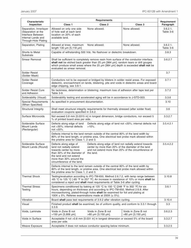
CharacteristicInspection
RequirementsRequirement
ParagraphClass 1 Class 2 Class 3
Separation, Innerlayer(Separation at theInterface BetweenInternal Lands andThrough-Hole Plating
Allowed on only one sideof hole wall at each landlocation on 20% of eachavailable land.
None allowed. None allowed. 3.6.2.1,Table 3-6
Separation, Plating Allowed at knee, maximumlength 130 µm [5,118 µin]
None allowed. None allowed. 3.6.2.1,Table 3-6
Shorts to MetalSubstrate
Capable of withstanding 500 Vdc. No flashover or dielectric breakdown. 3.8.3
Smear Removal Shall be sufficient to completely remove resin from surface of the conductor interface.shall not be etched back greater than 25 µm [984 µin]; random tears or drill gougeswhich produce small areas where the 25 µm [984 µin] depth is exceeded shall not beevaluated as smear removal.
3.6.2.7
Solder Resist(Solder Mask)
3.7
Solder ResistCoverage
Conductors not to be exposed or bridged by blisters in solder resist areas. For exposeddielectric, encroachment on lands, blistering, pits and voids in dielectric areas and boardedge chipping, see 3.8.1.
3.7.1
Solder Resist Cureand Adhesion
No tackiness, delamination or blistering; maximum loss of adhesion after tape test perTable 3-9.
3.7.2
Solderability (Visual) Solderability testing and accelerated aging will be in accordance to J-STD-003. 3.3.6
Special Requirements(When Specified)
As specified in procurement documentation. 3.10
Structural Integrity Shall meet structural integrity requirements for thermally stressed (after solder float)evaluation coupons specified in 3.6.2.
3.6
Surface Microvoids Not exceed 0.8 mm [0.0315 in] in longest dimension, bridge conductors, nor exceed 5% of printed board area per side.
3.3.2.7
Solderable SurfaceMount Lands(Rectangular)
Defects along edge of landnot >30%; internal defectsnot >20%.
Defects along edge of land not >20%; internal defects not>10%.
3.5.4.2.1
Defects internal to the land remain outside of the central 80% of the land width by80% of the land length, or pristine area. One electrical test probe mark allowed withinthe pristine area for Class 1, 2 and 3.
Solderable SurfaceMount Lands (Round)
Defects along edge ofland not radially extendtowards center by morethan 30% of the diameter ofthe land and not extendmore than 30% around thecircumference of the land.
Defects along edge of land not radially extend towardscenter by more than 20% of the diameter of the landand not extend more than 20% of the circumference ofthe land.
3.5.4.2.2
Defects internal to the land remain outside of the central 80% of the land width by80% of the land length, or pristine area. One electrical test probe mark allowed withinthe pristine area for Class 1, 2 and 3.
Thermal Shock Testing/evaluation according to IPC-TM-650, Method 2.6.7.2, with temp range between-65 °C to 125 °C [-85 °F to 257 °F]. An increase in resistance of 10% or more shall beconsidered a reject and shall meet requirements of Table 3-6 after cycling.
3.10.8
Thermal StressTesting
Specimens conditioned by baking at 120 °C to 150 °C [248 °F to 302 °F] for sixhours, depending on thickness and according to IPC-TM-650, Method 2.6.8. Aftermicrosectioning, plated-through holes shall be examined for foil and plating at100X ± 5%. Referee examinations made at 200X (± 5%).
3.6.1
Vibration Board shall pass test requirements of 3.9.2 after vibration cycling. 3.10.4
Visual Finished product shall be examined, be of uniform quality, and conform to 3.3.1 through3.3.9.
3.3
Voids, Laminate Voids in Zone B not>150 µm [5,906 µin].
Voids in Zone B not>80 µm [3,150 µin].
Voids in Zone B not>80 µm [3,150 µin].
3.6.2.3
Voids in Surface Acceptable if not >0.8 mm [0.031 in] in longest dimension or exceed 5% of the boardarea per side.
3.3.2.7
Weave Exposure Acceptable if does not reduce conductor spacing below minimum. 3.3.2.5
January 2007 IPC-6012B with Amendment 1
39

CharacteristicInspection
RequirementsRequirement
ParagraphClass 1 Class 2 Class 3
Wicking 125 µm[4,921 µin] maximum
100 µm[3,937 µin] maximum
80 µm[3,150 µin] maximum
3.6.2.1,Table 3-6
Wire Bond Pads Final conductor finish as specified in 1.3.4.2 for GWB-1, GWB-2 or ENIG. Final finishcoating per Table 3-2 for applicable coating. Pristine area shall have maximum surfaceroughness of 0.8 µm [32 µin] RMS as measured in accordance with Method 2.4.15. Nopits, nodules, scratches, electrical test probe marks within the pristine area that violatesRMS requirement.
3.5.4.3
Workmanship Shall be free of defects and of uniform quality - no visual of dirt, foreign matter, oil,fingerprints.
3.3.9
IPC-6012B with Amendment 1 January 2007
40

ANSI/IPC-T-50 Terms and Definitions forInterconnecting and Packaging Electronic CircuitsDefinition Submission/Approval Sheet
The purpose of this form is to keepcurrent with terms routinely used inthe industry and their definitions.Individuals or companies areinvited to comment. Pleasecomplete this form and return to:
IPC3000 Lakeside Drive, Suite 309SBannockburn, IL 60015-1249Fax: 847 615.7105
SUBMITTOR INFORMATION:
Name:
Company:
City:
State/Zip:
Telephone:
Date:
❑ This is a NEW term and definition being submitted.❑ This is an ADDITION to an existing term and definition(s).❑ This is a CHANGE to an existing definition.
Term Definition
If space not adequate, use reverse side or attach additional sheet(s).
Artwork: ❑ Not Applicable ❑ Required ❑ To be supplied
❑ Included: Electronic File Name:
Document(s) to which this term applies:
Committees affected by this term:
Office UseIPC Office Committee 2-30
Date Received:Comments Collated:Returned for Action:Revision Inclusion:
Date of Initial Review:Comment Resolution:Committee Action: ❑ Accepted ❑ Rejected
❑ Accept Modify
IEC ClassificationClassification Code • Serial Number
Terms and Definition Committee Final Approval Authorization:Committee 2-30 has approved the above term for release in the next revision.
Name: Committee: Date:IPC 2-30
ASSOCIATION CONNECTINGELECTRONICS INDUSTRIES ®

This Page Intentionally Left Blank

Technical QuestionsThe IPC staff will research your technical question and attempt to find an appropriate specificationinterpretation or technical response. Please send your technical query to the technical department via:
tel: 847-615-7100 fax: 847-615-7105 www.ipc.org e-mail: [email protected]
IPC World Wide Web Page www.ipc.orgOur home page provides access to information about upcoming events, publications and videos, membership, and industryactivities and services. Visit soon and often.
IPC Technical ForumsIPC technical forums are opportunities to network on the Internet. It’s the best way to get the help you need today! Over2,500 people are already taking advantage of the excellent peer networking available through e-mail forums provided by IPC.Members use them to get timely, relevant answers to their technical questions. Contact [email protected] for details.Here are a few of the forums offered.
[email protected] forum is for discussion of issues related to printed circuit board design, assembly, manufacturing, comments orquestions on IPC specifications, or other technical inquiries. IPC also uses TechNet to announce meetings, important technicalissues, surveys, etc.
[email protected] forum covers environmental, safety and related regulations or issues.
[email protected] Council forum covers information on upcoming IPC Designers Council activities as well as information, comments,and feedback on current designer issues, local chapter meetings, new chapters forming, job opportunities and certification. Inaddition, IPC can set up a mailing list for your individual Chapter so that your chapter can share information about upcomingmeetings, events and issues related specifically to your chapter.
[email protected] This is an announcement forum where subscribers can receive notice of new IPC Training Products.
leadfree.ipc.orgThis forum acts as a peer interaction resource for staying on top of lead elimination activities worldwide and within IPC.
[email protected] is an announcement forum where subscribers can receive notice of new IPC publications, updates and standards.
ADMINISTERING YOUR SUBSCRIPTION STATUS:All commands (such as subscribe and signoff) must be sent to [email protected]. Please DO NOT send any command to themail list address, (i.e.<mail list> @ipc.org), as it would be distributed to all the subscribers.
Example for subscribing: Example for signing off:To: [email protected] To: [email protected]: Subject:Message: subscribe TechNet Joseph H. Smith Message: signoff DesignerCouncil
Please note you must send messages to the mail list address ONLY from the e-mail address to which you want to applychanges. In other words, if you want to sign off the mail list, you must send the signoff command from the address that youwant removed from the mail list. Many participants find it helpful to signoff a list when travelling or on vacation and toresubscribe when back in the office.
How to post to a forum:To send a message to all the people currently subscribed to the list, just send to <mail list>@ipc.org. Please note, use the maillist address that you want to reach in place of the <mail list> string in the above instructions.
Example:To: [email protected]: <your subject>Message: <your message>
The associated e-mail message text will be distributed to everyone on the list, including the sender. Further information onhow to access previous messages sent to the forums will be provided upon subscribing.For more information, contact Keach Sasamoritel: 847-597-2815 fax: 847-615-5615e-mail: [email protected] www.ipc.org/emailforums
BE
NE
FIT
S O
F IP
C M
EM
BE
RS
HIP

Education and TrainingIPC conducts local educational workshops and national conferences to help you better understand conventional and
emerging technologies. Members receive discounts on registration fees. Visit www.ipc.org to see what programs are
coming to your area.
IPC Certification ProgramsIPC provides world-class training and certification programs based on several widely-used IPC standards, including
IPC-A-600, IPC-A-610, IPC/WHMA-A-620, J-STD-001 and IPC-7711A/7721A Rework and Repair. IPC-sponsored
certification gives your company a competitive advantage and your workforce valuable recognition.
For more information on these programs:
tel: 847-597-2814 fax: 847-615-7105
e-mail: [email protected] www.ipc.org/certification
Designer Certification (C.I.D.)/Advanced Designer Certification (C.I.D.+)Contact:
tel: 847-597-2827 fax: 847-615-5627
e-mail: [email protected] http://dc.ipc.org
EMS Program Manager CertificationContact:
tel: 847-597-2884 fax: 847-615-5684
e-mail: [email protected] www.ipc.org/certification
IPC Video Tapes and CD-ROMsIPC video tapes and CD-ROMs can increase your industry know-how and on the job effectiveness. Members receive
discounts on purchases.
For more information on IPC Video/CD Training, contact Mark Pritchard
tel: 505/758-7937 ext. 202 fax: 505/758-7938
e-mail: [email protected] http://training.ipc.org
IPC Printed Circuits Expo, APEX and the Designers SummitThis yearly event is the largest electronics interconnection event in North America. With technical
paper presentations, educational courses, standards development meetings networking opportunities
and designers certification, there’s something for everyone in the industry. The premier technical
conference draws experts from around the globe. 500 exhibitors and 6,000 attendees typically
participate each year. You’ll see the latest in technologies, products and services and hear about the trends that affect us
all. Go to www.GoIPCShows.org or contact [email protected] for more information.
Exhibitor information:Mary Mac Kinnon Alicia Balonek
Director, Show Sales Director, Trade Show Operations
847-597-2886 847-597-2898
MaryMacKinnon@ip c.org [email protected]
How to Get InvolvedThe first step is to join IPC. An application for membership can be found in the back of this publication. Once you
become a member, the opportunities to enhance your competitiveness are vast. Join a technical committee and learn
from our industry’s best while you help develop the standards for our industry. Participate in market research programs
which forecast the future of our industry. Participate in Capitol Hill Day and lobby your Congressmen and Senators for
better industry support. Pick from a wide variety of educational opportunities: workshops, tutorials, and conferences.
More up-to-date details on IPC opportunities can be found on our web page: www.ipc.org.
For information on how to get involved, contact:
Jeanette Ferdman, Membership Director
tel: 847-597-2809 fax: 847-597-7105
e-mail: [email protected] www.ipc.org
BE
NE
FIT
S O
F I
PC
ME
MB
ER
SH
IP

� Government Agencies/Academic Technical Liaisons
We are representatives of a government agency, university, college, technical institute who are directly concerned with design, research, and utilization of electronic interconnection devices. (Must be a non-profit or not-for-profit organization.)
� One-sided and two-sided rigid printed boards
� Multilayer printed boards
� Flexible printed boards
� Other interconnections
What is your company’s primary product line? ______________________________________________________
� Independent Electronic Assembly EMSI Companies
This facility assembles printed wiring boards, on a contract basis, and may offer other electronic interconnectionproducts for sale.
� Industry Suppliers
This facility supplies raw materials, machinery, equipment or services used in the manufacture or assembly ofelectronic interconnection products.
Thank you for your decision to join IPC members on the “Intelligent Path to Competitiveness”!IPC Membership is site specific, which means that IPC member benefits are available to allindividuals employed at the site designated on the other side of this application.
To help IPC serve your member site in the most efficient manner possible, please tell us whatyour facility does by choosing the most appropriate member category. (Check one box only.)
� Independent Printed Board Manufacturers
This facility manufactures and sells to other companies, printed wiring boards (PWBs) or other electronicinterconnection products on the merchant market. What products do you make for sale?
Name of Chief Executive Officer/President________________________________________________________
What products do you supply?__________________________________________________________________
ASSOCIATION CONNECTINGELECTRONICS INDUSTRIES ®
Application for Site Membership
Name of Chief Executive Officer/President________________________________________________________
� OEM–Manufacturers of any end product using PCB/PCAs or Captive Manufacturers of PCBs/PCAs
This facility purchases, uses and/or manufactures printed wiring boards or other interconnection products foruse in a final product, which we manufacture and sell.

Application for Site Membership
Please attach business card
of primary contact here
Please Check One:
� $1,000.00 Annual dues for Primary Site Membership (Twelve months of IPCmembership begins from the time the application and payment are received)
� $800.00 Annual dues for Additional Facility Membership: Additional membership for a site within anorganization where another site is considered to be the primary IPC member.
� $600.00** Annual dues for an independent PCB/PWA fabricator or independent EMSI provider withannual sales of less than $1,000,000.00. **Please provide proof of annual sales.
� $250.00 Annual dues for Government Agency/not-for-profit organization
TMRC Membership � Please send me information about membership in the Technology MarketResearch Council (TMRC)
Mail application with check or money order to:IPC3491 Eagle WayChicago, IL 60678-1349
Fax/Mail application with credit card payment to:IPC3000 Lakeside Drive, Suite 309 S Bannockburn, IL 60015-1249Tel: 847-615-7100Fax: 847-615-7105http://www.ipc.org
Payment Information:
Enclosed is our check for $________________
Please bill my credit card: (circle one) MC AMEX VISA DINERS
Card No.___________________________________________________________Exp date_______________
Authorized Signature________________________________________________________________________________
Site Information:
Company Name
Street Address
City State Zip/Postal Code Country
Main Switchboard Phone No. Main Fax
Name of Primary Contact
Title Mail Stop
Phone Fax e-mail
Company e-mail address W
ebsite URL
ASSOCIATION CONNECTINGELECTRONICS INDUSTRIES ®

Standard Improvement Form IPC-6012B with Amendment 1The purpose of this form is to provide theTechnical Committee of IPC with inputfrom the industry regarding usage ofthe subject standard.
Individuals or companies are invited tosubmit comments to IPC. All commentswill be collected and dispersed to theappropriate committee(s).
If you can provide input, please completethis form and return to:
IPC3000 Lakeside Drive, Suite 309SBannockburn, IL 60015-1249Fax 847 615.7105E-mail: [email protected]
1. I recommend changes to the following:
Requirement, paragraph number
Test Method number , paragraph number
The referenced paragraph number has proven to be:
Unclear Too Rigid In Error
Other
2. Recommendations for correction:
3. Other suggestions for document improvement:
Submitted by:
Name Telephone
Company E-mail
Address
City/State/Zip Date
ASSOCIATION CONNECTINGELECTRONICS INDUSTRIES

ASSOCIATION CONNECTINGELECTRONICS INDUSTRIES
3000 Lakeside Drive, Suite 309S, Bannockburn, IL 60015-1249Tel. 847.615.7100 Fax 847.615.7105
www.ipc.org
®