Embed Size (px)
Citation preview

Principles and Applications of Electronic Devices and Circuits
Assignment 1 40764/01
It's very straightforward to submit this test paper online by logging on to the ICSStudent Community at www.icslearn.co.uk.
For guidance on submitting test papers online, please see the Help>Assessment sectionof the Student Community.
Evidence you need to provide from this unit:
1 Written reports where requested.
2 Photographs where requested, with you in the picture.
3 Video footage of your circuits being built. Video must show you in the video.
4 Video footage of your circuits being tested. Video must show you in the video.
You will find a table showing the assessment criteria for this unit at the end of theassessment tasks.
40764A 141

BTEC Level 3 Certificate in Electronic Engineering
Task 1
Principles and Applications of Electronic Devices and Circuits:Analogue Circuits
The Assignment Criteria for this task are:
P1 Explain the purpose of two different types of diode, each in a different electroniccircuit application
P2 Explain the operation of two different types of transistor, one in an analogue andone in a digital circuit
M1 Modify an existing analogue circuit to achieve a given revised specification byselecting and changing the value of one of the components (merit criterion).
Context
Your employer is developing a new battery-powered product, one which requires a 6 Vsupply and an LED operated by a digital circuit.
You are required to construct and test two analogue circuits. One is a voltage regulatorusing a Zener diode for stabilisation. The other is a transistor wired as a switch.
Circuit Build
You can obtain credit towards a pass grade for this unit by successfully completingquestions 1 and 2 and completing the report as requested.
You can obtain credit towards a merit grade for this unit by successfully completingquestions 1, 2 and 3 and completing the report as requested.
1 Zener Diode Circuit
Build the circuit below on breadboard.
loadvoltage9V —±r
J
Figure 5.1: Voltage regulator circuit
142 40764A
Principles and Applications of Electronic Devices and Circuits
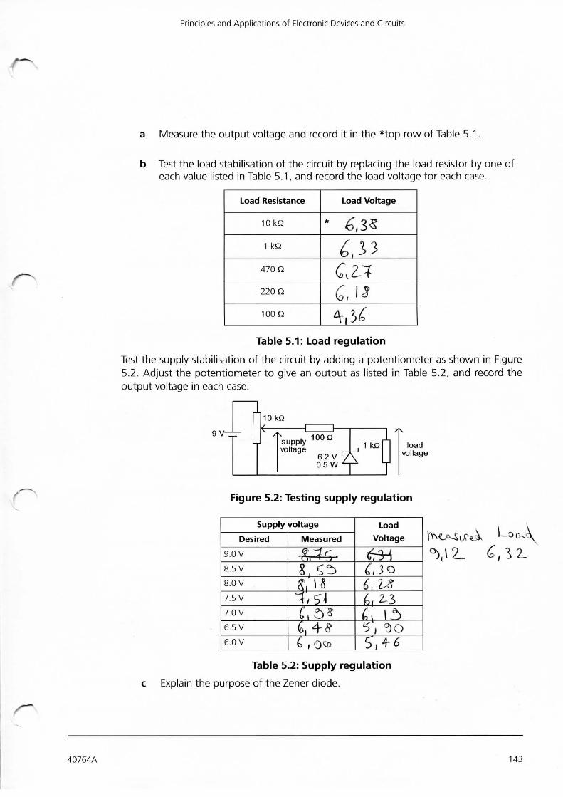
Measure the output voltage and record it in the *top row of Table 5.1.
Test the load stabilisation of the circuit by replacing the load resistor by one ofeach value listed in Table 5.1,and record the load voltage for each case.
Load Resistance Load Voltage
10 kQ * 6,351 k£2
470 Q CZT220 £2
100 Q
Table 5.1: Load regulation
Test the supply stabilisation of the circuit by adding a potentiometer as shown in Figure5.2. Adjust the potentiometer to give an output as listed in Table 5.2, and record theoutput voltage in each case.
9V-±
10 kQ
«" >supplyvoltage
100 Q
6.2 V0.5 W
1 kQi
j
loadvoltage
Figure 5.2: Testing supply regulation
Supply voltage Load
VoltageDesired Measured
9.0 V -SrlA-8.5 V
8.0 V t 1 5 6, IS7.5 V 4,51 L ÿ37.0 V E.6S C ,6.5 V 6, 4-4 5, °)Q6.0 V 6 , 5,4-6
Table 5.2: Supply regulation
c Explain the purpose of the Zener diode.
(jrÿ 3c-\
3 2-
40764A 143

BTEC Level 3 Certificate in Electronic Engineering
2 Transistor Circuit
Build the circuit below on breadboard and check that the LED is illuminated.
330 Q
22 kQ V
BC108
IT +9 V
/
\
basevj/
©emitter collector
Figure 5.3: LED circuit Figure 5.4: BC108 transistor(as seen from below)
Record the voltages listed in Table 5.3, and use them to calculate the currents.
Voltages Currents
Supply 3,12-V base base J ALED /, rzi/ collector 0,103V collector
Table 5.3: LED voltages and currents
Explain the purpose of the LED and the transistor in the circuit.
To achieve a merit grade and satisfy assessment criteria M1: You can obtain credittowards a merit for this unit by modifying the circuit.
3 Modify the circuit
Modify your circuit so that the LED current is approximately 10 mA, and completeTable 5.4, filling in the voltages measured on your new circuit.
Voltages Currents
Supply °)MV base o(Tz/ base 0,5 twALED collector TOkI/ collector 1J A
Table 5.4: modified circuit
Report
a Explain how the Zener diode circuit acts as a voltage stabiliser, with referenceto your measurements.
b Explain how the transistor circuit can be used to allow digital logic to operatean LED with reference to the currents flowing in the test circuit(s).
V
144 40764A
Principles and Applications of Electronic Devices and Circuits
'
n
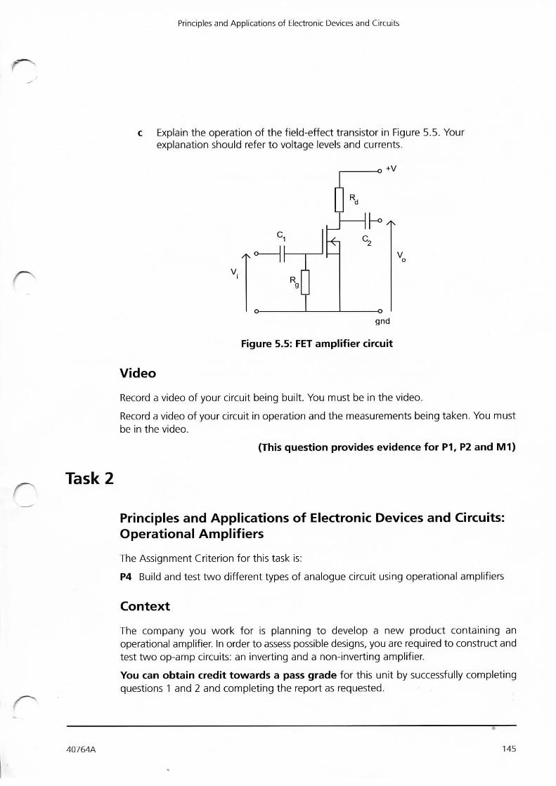
c Explain the operation of the field-effect transistor in Figure 5.5. Yourexplanation should refer to voltage levels and currents.
+v
V. I
R,
fh /K
R
gnd
Figure 5.5: FET amplifier circuit
Video
Record a video of your circuit being built. You must be in the video.
Record a video of your circuit in operation and the measurements being taken. You mustbe in the video.
(This question provides evidence for P1, P2 and M1)
Task 2
Principles and Applications of Electronic Devices and Circuits:Operational Amplifiers
The Assignment Criterion for this task is:
P4 Build and test two different types of analogue circuit using operational amplifiers
Context
The company you work for is planning to develop a new product containing anoperational amplifier. In order to assess possible designs, you are required to construct andtest two op-amp circuits: an inverting and a non-inverting amplifier.
You can obtain credit towards a pass grade for this unit by successfully completingquestions 1 and 2 and completing the report as requested.
40764A 145
BTEC Level 3 Certificate in Electronic Engineering
Circuit Build
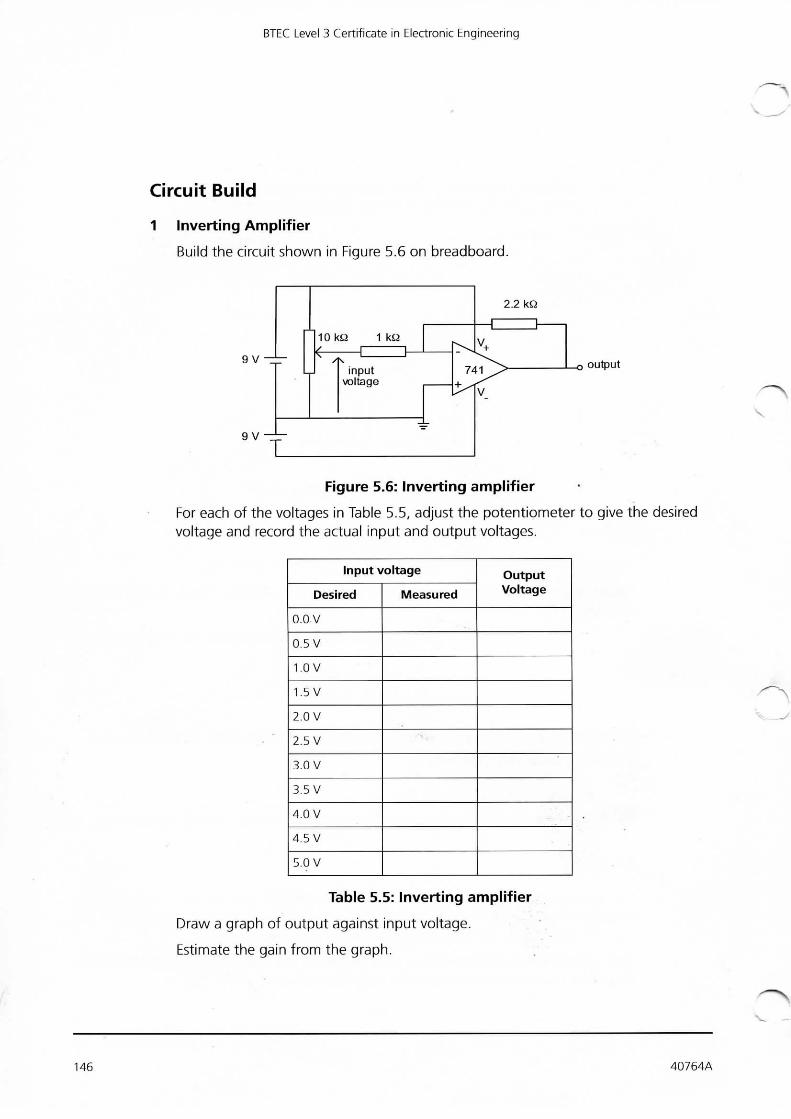
1 Inverting Amplifier
Build the circuit shown in Figure 5.6 on breadboard.
2.2 kQ
Outputinputvoltage
Figure 5.6: Inverting amplifier
For each of the voltages in Table 5.5, adjust the potentiometer to give the desiredvoltage and record the actual input and output voltages.
Input voltage OutputVoltageDesired Measured
0.0 V
0.5 V
1.0 V
1.5 V
2.0 V
2.5 V
3.0 V
3.5 V
4.0 V
4.5 V
5.0 V
Table 5.5: Inverting amplifier
Draw a graph of output against input voltage.
Estimate the gain from the graph.
146 40764A

Principles and Applications of Electronic Devices and Circuits
2 Non-inverting Amplifier
This amplifier circuit is intended to produce a large gain. As a result, the inputsignal would need to be too small for a digital multimeter to read, so a voltagedivider is used to attenuate the input by a factor of around 100.
Build the circuit shown in Figure 5.7 on breadboard.
input/1000o—[
input _o output
22 kQ
100 Q
9 V "±"100 Q
9 v
Figure 5.7: Non-inverting amplifier
Use an ac source to generate a signal for each of the frequencies in Table 5.6, andmeasure the input and output voltages.
Frequency Input Voltage Output Voltage Gain
50 Hz
100 Hz
200 Hz
500 Hz
1 kHz
2 kHz
5 kHz
10 kHz
Table 5.6: Non-inverting amplifier
Calculate the voltage at the amplifier's non-inverting input, and hence the gain foreach data point in the experiment.
Draw a graph of gain against input frequency.
40764A 147

BTEC Level 3 Certificate in Electronic Engineering
Report
Compare the results of the two experiments to those predicted by theory. Estimatethe bandwidth for the second amplifier, describing how you arrived at your value.
Your report should include tables of results and graphs, and comment on anydiscrepancies.
VideoRecord a video of your circuit being built. You must be in the video.
Record a video of your circuit in operation and the measurements being taken. You must
be in the video.
(This question provides evidence for P4)
Task 3
Principles and Applications of Electronic Devices and Circuits:Digital Circuits
The Assignment Criteria for this task are:
P3 Explain the operation of three different logic gates with appropriate gate symbols,truth tables and Boolean expressions
P5 Build and test a combinational logic circuit that has three input variables
P6 Build and test a sequential circuit using integrated circuit(s)
M2 Modify a digital circuit to achieve a given revised specification by selecting andchanging up to two logic gates (merit criterion)
M3 Evaluate and minimise a three-input combinational logic circuit containing threegates (merit criterion)
D2 Compare and contrast two different types of logic family with reference to fivecharacteristics (distinction criterion).
Context
Your employer is developing safety equipment for an industrial machine. The first part ofthe circuit displays an alarm if certain conditions are not in place. The second counts thenumber of times the alarm has been triggered.
You are required to build two prototype circuits on breadboard to ensure that they operateas required.
Firstly, explain the operation of three different logic gates with appropriate gate symbols,truth tables and Boolean expressions.
148 40764A

Principles and Applications of Electronic Devices and Circuits
Circuit Build
You can obtain credit towards a pass grade for this unit by successfully completingquestions 1 and 2 and completing the report as requested.
You can obtain credit towards a merit grade for this unit by successfully completingquestion 1, 2 and 3 and completing the report as requested.
1 Combinational Logic
Build the combinational logic circuit shown in Figure 5.8 on a breadboard, taking anote of pin numbers for all the gates used.
A
B
c
Figure 5.8: Safety system logic
Test the circuit by setting A = 0B=1 C = 0. Record the input(s) and outputs ofevery gate, as measured by a logic probe.
Complete Table 5.7, recording the status of the output for each combination oflogic inputs.
A B c Desired X Recorded X
0 0 0 1
0 0 1 1
0 1 0 1
0 1 1 1
1 0 0 0
1 0 1 0
1 1 0 1
1 1 1 0
Table 5.7: Safety system results
40764A 149

BTEC Level 3 Certificate in Electronic Engineering
2 Sequential Logic
Build the SR latch circuit shown in Figure 5.9 on a breadboard and check that itoperates correctly.
+5 v
10 KQ10 KQ
"ÿoutput
set o\ o reset
switch
Figure 5.9: Debounced switch
Then, build the 3-bit counter circuit shown in Figure 5.10 on a breadboard, usingthe output from your latch as a clock input.
+5 v
_n_ 0.
clr clr clr
clock fromdebounced switch
Figure 5.10: Counter circuit
Test the circuit by using a logic probe to determine the output from each bit of thecounter as the clock input is taken high then low.
Record the results in the form of a waveform diagram.
To achieve a merit grade
You can obtain credit towards a merit grade for this unit by successfully redesigningthe circuit.
150 40764A

Principles and Applications of Electronic Devices and Circuits
Redesigning the circuit
The new circuit must have the output inverted, as shown in Table 5.8. Also, you arerequired to use logic minimisation methods to design the simplest possible circuit.
Build your new circuit and test it, recording the results in Table 5.8.
A B c Desired X Recorded X
0 0 0 0
0 0 1 0
0 1 0 0
0 1 1 0
1 0 0 1
1 0 1 1
1 1 0 0
1 1 1 1
Table 5.8: Redesigned circuit
Report
To achieve a pass grade your report should include:
• Tables of results
• Circuit diagram for minimised circuit (if attempted)
• Waveform diagram for counter circuitShow that your circuits are working correctly.
To achieve a distinction grade your report should include:
Compare and contrast TTL and CMOS logic with reference to characteristics such as
• Supply voltage
• Input and output voltages
• Input and output current
• Speed
• Power.
Use an inverter ic as an example and quote specific values. You must state the sources ofinformation.
(This task provides evidence for D2)
40764A 151
BTEC Level 3 Certificate in Electronic Engineering
VideoRecord a video of your circuit being built. You must be in the video.
Record a short video of your circuit in operation and the measurements being taken. Youmust be in the video.
(This task provides evidence for P3, P5, P6, M2, M3 and D2)
Task 4
Principles and Applications of Electronic Devices and Circuits:Simulation
The Assignment Criteria for this task are:
P7 Use a computer software package to simulate the construction and testing of ananalogue circuit with three different types of components
P8 Use a computer software package to simulate the construction and testing of adigital logic circuit with three gates
D1 Using a simulation package, analyse the effects of changing the values of circuitparameters on the performance of an analogue circuit containing an operationalamplifier or transistors (distinction criterion)
Context
You are required to simulate two circuits using a computer package, one analogue andone digital. The analogue circuit will be a simple active filter, while the digital circuit willbe a combinational logic circuit.
You can obtain credit towards a pass grade for this unit by successfully completingquestion 1.1 and 2 and completing the report as requested.
You can obtain credit towards a merit grade for this unit by successfully completingquestions 1.1, 1.2 and 2 and completing the report as requested.
1.1 Analogue Simulation
A low-pass filter circuit is required for use with a sound recording device youremployer is developing.
Simulate using a relevant simulation software package (such as LTSpice available at:http://www.linear.com/LTSpice) the filter design in Figure 5.11.
152 40764A

Principles and Applications of Electronic Devices and Circuits
22.5 nF
input
1 KQ 1 Kq 0 output
11.3 nF=ÿz
Figure 5.11: Low-pass filter
Produce a graph of output voltage against frequency in the range 1 kHz to 1 MHz. andprint it out.
To achieve a distinction grade:
1.2 You can obtain credit towards a distinction for this unit by successfullyanswering the question below.
Produce two more graphs, replacing the 11 nF capacitor with:
a 47 nFb 0.47 nF
Analyse (i.e. examine in detail in order to explain) the effect of replacing the 11 nFcapacitor.
2 Digital Simulation
Simulate using a relevant simulation software package (such as LTSpice available at:http://www.linear.com/LTSpice) the digital circuit design in Figure 5.12.
This circuit is required for an alarm to be fitted to a car. A warning chime is tosound whenever the driver opens the door with the lights on but the ignition off.
Figure 5.12: Car light warning system
Test the circuit by running through all eight possible combinations of input andrecording the output in Table 5.9.
door open Q-
ignition on q-
lights on q.
chime
40764A 153

BTEC Level 3 Certificate in Electronic Engineering
Door Open Ignition On Lights On Chime
0 0 0 0
0 0 1 0
0 1 0 0
0 1 1 0
1 0 0 0
1 0 1 1
1 1 0 0
1 1 1 0
Table 5.9: Car light warning system
Then, record the input and output waveforms while simulating the following driveractions:
• Ignition turned on
• Lights turned on
• Ignition turned off
• Door opened
• Door shut
• Lights turned on
• Door opened.
Print out the waveforms, ensuring that all of the test data is visible.
Report
Your report should include:
• Printouts of both circuits
• The graph of gain against frequency for the filter
• An estimate of the gain and bandwidth of the filter, along with an explanation ofhow you arrived at these figures
• Completed truth table for the car warning system
• A waveform diagram along with a description indicating what the driver is doingand showing that the chime is operating correctly.
To achieve a pass with distinction, your report should also analyse the effects ofchanging component values on the performance of the filter circuit.
(This task provides evidence for P7, P8 and D1)
154 40764A

Principles and Applications of Electronic Devices and Circuits
In this assessment you will have opportunities to provide evidence against the followingassessment and grading criteria:
r
To achieve a pass grade theevidence must show that thelearner is able to:
To achieve a merit grade theevidence must show that, inaddition to the pass criteria,the learner is able to:
To achieve a distinctiongrade the evidence mustshow that, in addition to thepass and merit criteria, thelearner is able to:
PI Explain the purpose of twodifferent types of diode, each ina different electronic circuitapplication
M1 Modify an existing analoguecircuit to achieve a given revisedspecification by selecting andchanging the value of one ofthe components
D1 Using a simulation package,analyse the effects of changingthe values of circuit parameterson the performance of ananalogue circuit containing anoperational amplifier ortransistors
P2 Explain the operation of twodifferent types of transistor, onein an analogue and one in adigital circuit
M2 Modify a digital circuit toachieve a given revisedspecification by selecting andchanging up to two logic gates
D2 Compare and contrast twodifferent types of logic familywith reference to fivecharacteristics
P3 Explain the operation ofthree different logic gates withappropriate gate symbols, truthtables and Boolean expressions
M3 Evaluate and minimise athree-input combinational logiccircuit containing three gates
P4 Build and test two differenttypes of analogue circuit usingoperational amplifiers
P5 Build and test acombinational logic circuit thathas three input variables
P6 Build and test a sequentialcircuit using integrated circuit(s)
P7 Use a computer softwarepackage to simulate theconstruction and testing of ananalogue circuit with threedifferent types of components
P8 Use a computer softwarepackage to simulate theconstruction and testing of adigital logic circuit with threegates
Now send your answers to ICS.
40764A 155

BTEC Level 3 Certificate in Electronic Engineering
156 40764A