Embed Size (px)
Citation preview

1
Assessing the Impact of RTN on Logic Timing Margin Using a 32nm
Dual Ring Oscillator Array
Qianying Tang and Chris H. Kim
University of Minnesota, Minneapolis
{tangx280, chriskim}@umn.edu

2
Outline of Presentation
• RTN (Random Telegraph Noise) Impact on Logic Timing
• Proposed Dual Ring Oscillator Array RTN Monitor
• 32nm Test Chip Results
• Timing Margin Analysis
• Conclusions
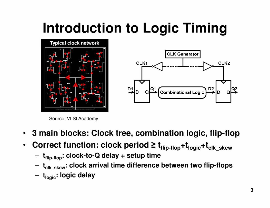
Introduction to Logic Timing
3
• 3 main blocks: Clock tree, combination logic, flip-flop
• Correct function: clock period ≥ tflip-flop+tlogic+tclk_skew
– tflip-flop: clock-to-Q delay + setup time
– tclk_skew: clock arrival time difference between two flip-flops
– tlogic: logic delay
Source: VLSI Academy
Typical clock network
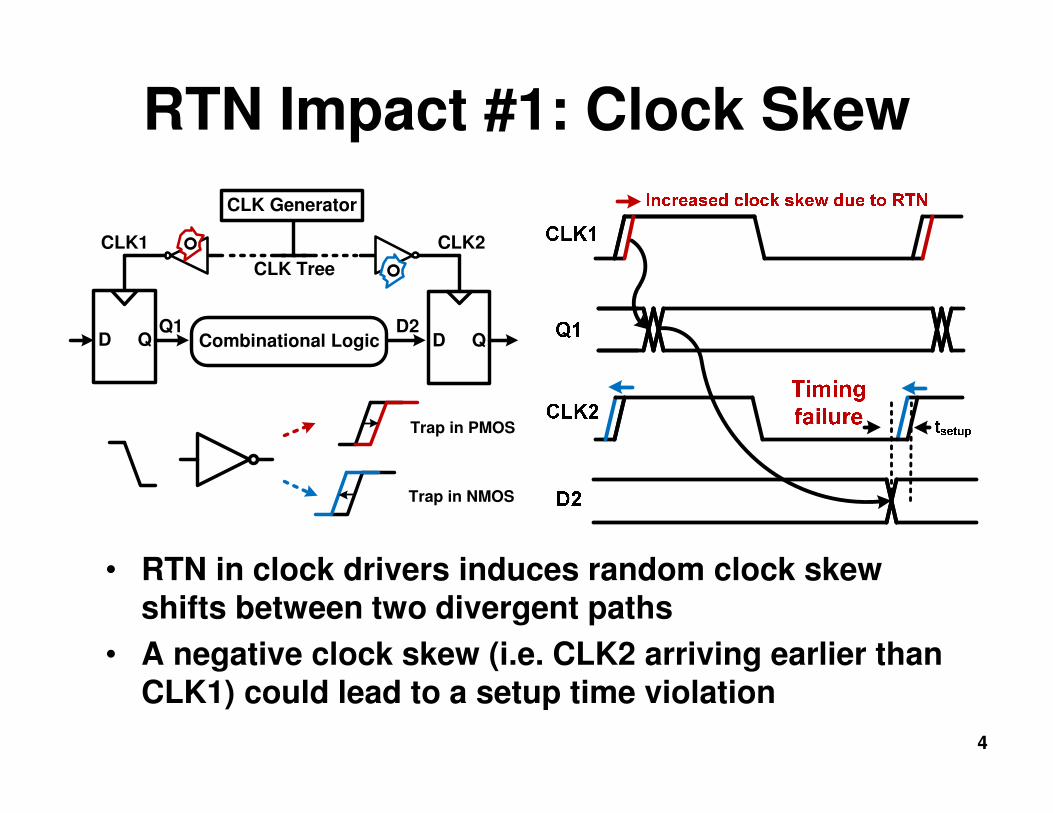
RTN Impact #1: Clock Skew
4
• RTN in clock drivers induces random clock skew shifts between two divergent paths
• A negative clock skew (i.e. CLK2 arriving earlier than CLK1) could lead to a setup time violation
D Q Combinational Logic D Q
CLK Generator
CLK Tree
Q1 D2
CLK1 CLK2
Trap in PMOS
Trap in NMOS
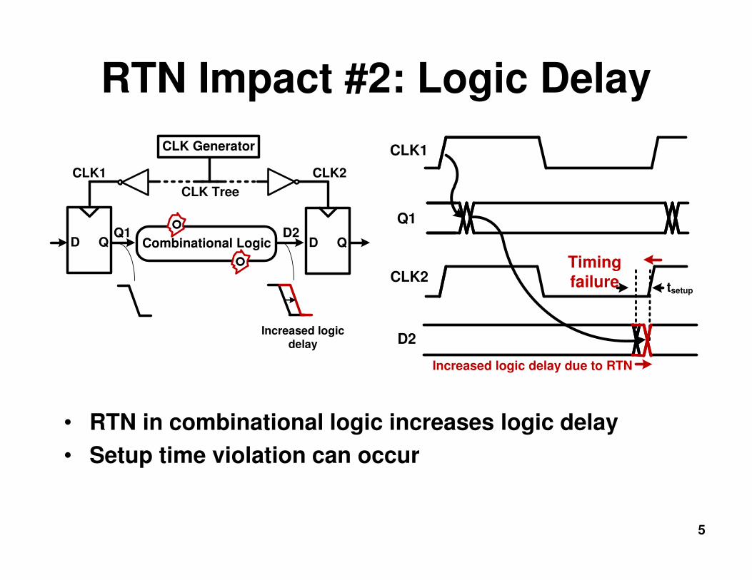
RTN Impact #2: Logic Delay
5
D Q Combinational Logic D Q
CLK Generator
CLK Tree
Q1 D2
CLK1 CLK2
Increased logic delay
• RTN in combinational logic increases logic delay
• Setup time violation can occur
CLK1
Q1
D2
CLK2
Increased logic delay due to RTN
Timing failure tsetup
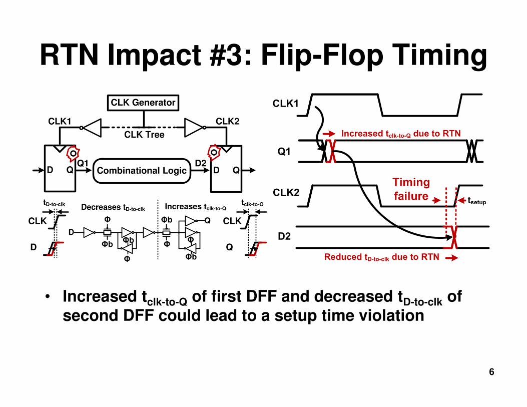
RTN Impact #3: Flip-Flop Timing
6
D Q Combinational Logic D Q
CLK Generator
CLK Tree
Q1 D2
CLK1 CLK2
Decreases tD-to-clk
D
QΦ
Φb Φb
Φ
Φ
Φb
Φb
Φ
Increases tclk-to-Q
CLK
D
tD-to-clk
CLK
Q
tclk-to-Q
• Increased tclk-to-Q of first DFF and decreased tD-to-clk of second DFF could lead to a setup time violation
CLK1
Q1
D2
CLK2
Increased tclk-to-Q due to RTN
Timing
failure tsetup
Reduced tD-to-clk due to RTN
7Q. Tang and C.H. Kim, VLSI Technology Symposium, 2013
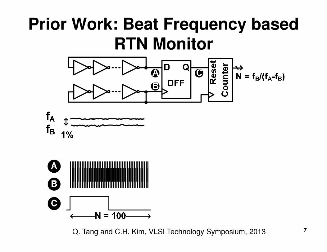
Prior Work: Beat Frequency based RTN Monitor
8Q. Tang and C.H. Kim, VLSI Technology Symposium, 2013
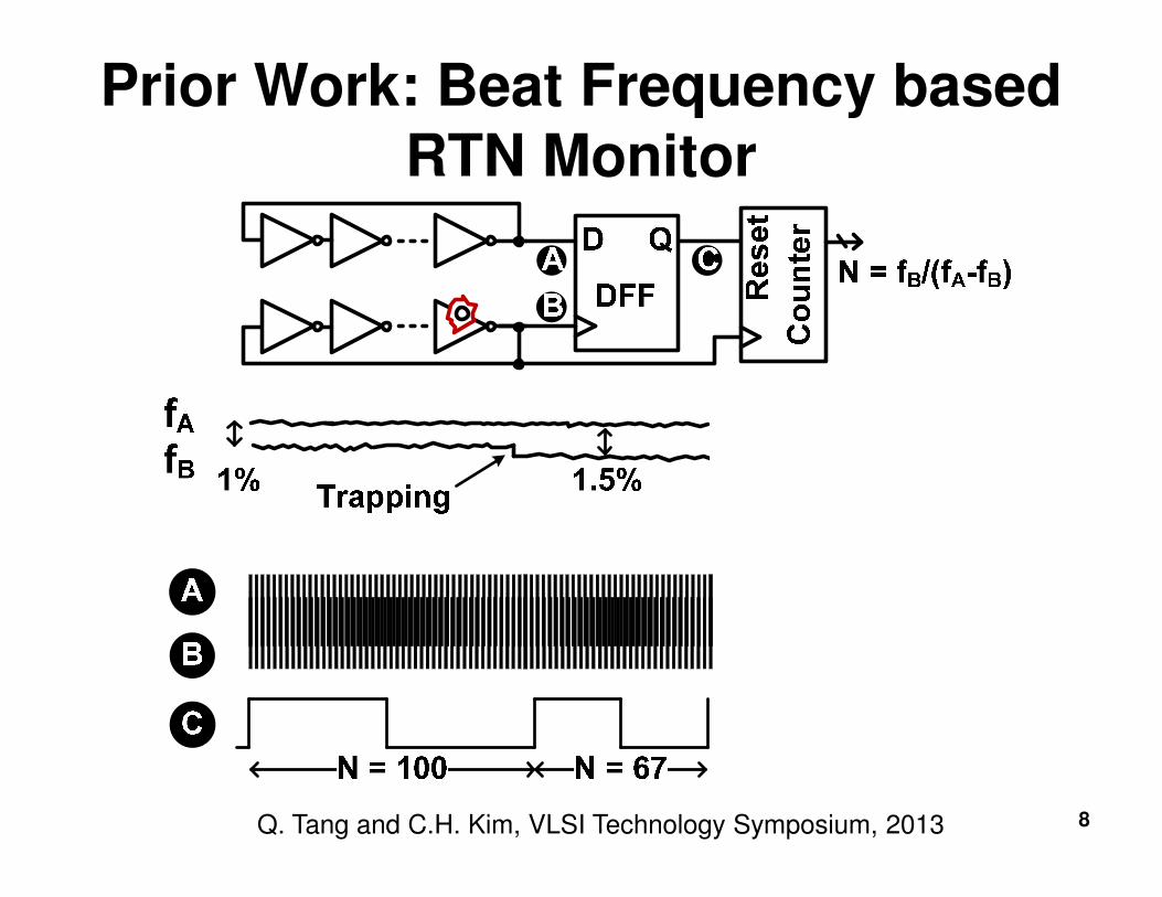
Prior Work: Beat Frequency based RTN Monitor

9
DFF
Co
un
ter
Res
et
D Q
B
A C
A
B
fA
fB 1%
C
1.5% 2%
N = 100 N = 67 N = 50
Trapping
N = fB/(fA-fB)
Trapping
Q. Tang and C.H. Kim, VLSI Technology Symposium, 2013
Prior Work: Beat Frequency based RTN Monitor
10
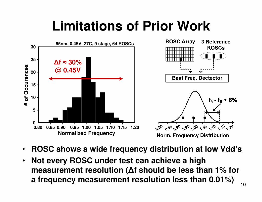
Limitations of Prior Work
• ROSC shows a wide frequency distribution at low Vdd’s
• Not every ROSC under test can achieve a high measurement resolution (Δf should be less than 1% for a frequency measurement resolution less than 0.01%)
0.80 0.85 0.90 0.95 1.00 1.05 1.10 1.15 1.200
5
10
15
20
25
30
# o
f O
ccu
ren
ce
s
Normalized Frequency
65nm, 0.45V, 27C, 9 stage, 64 ROSCs
Δf ≈ 30%@ 0.45V

11Q. Tang and C.H. Kim, VLSI Technology Symposium, 2013
Limitations of Prior Work
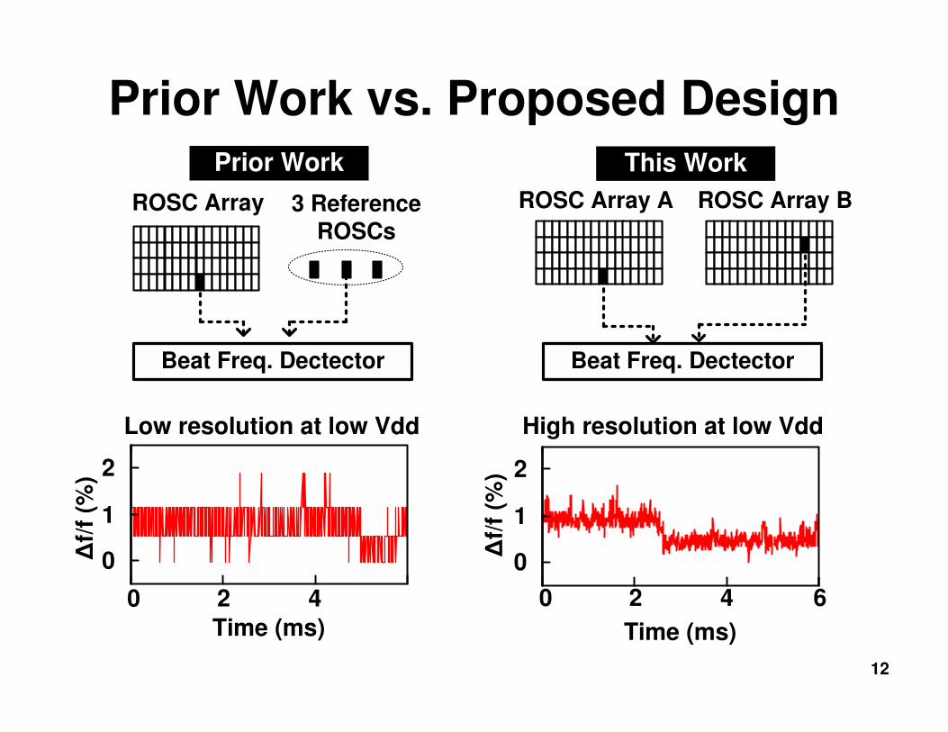
Prior Work vs. Proposed Design
12
0 2 4
0
1
2
Time (ms)
Δf/
f (%
)
Low resolution at low Vdd
0 2 4 6
0
1
2
Time (ms)
Δf/
f (%
)
High resolution at low Vdd
Prior Work This Work
Beat Freq. Dectector
3 Reference ROSCs
ROSC Array ROSC Array A ROSC Array B
Beat Freq. Dectector
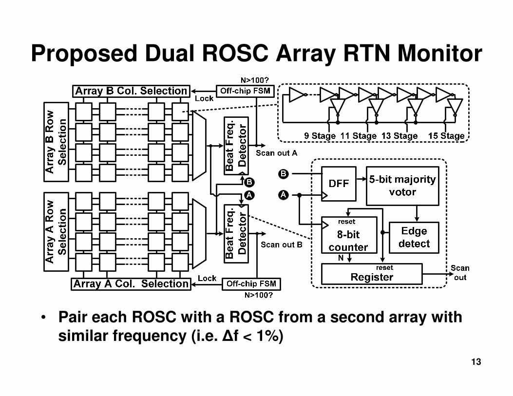
Proposed Dual ROSC Array RTN Monitor
13
• Pair each ROSC with a ROSC from a second array with similar frequency (i.e. Δf < 1%)
14
Outline of Presentation
• RTN Impact on Logic Timing
• Proposed Dual Ring Oscillator Array RTN Monitor
• 32nm Test Chip Results
• Timing Margin Analysis
• Conclusions
15
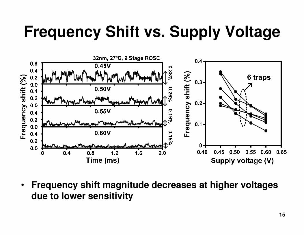
Frequency Shift vs. Supply Voltage
Fre
qu
en
cy
sh
ift
(%)
• Frequency shift magnitude decreases at higher voltages due to lower sensitivity

16
Frequency Shift vs. Temperature
• RTN trapping and de-trapping time constants become shorter at higher temperatures

17
Frequency Shift vs. ROSC Stages
• Frequency shift magnitude decreases for longer ROSCs
• Fewer measurable RTN traps in longer ROSCs
– More traps present but harder to detect due to averaging effect
18
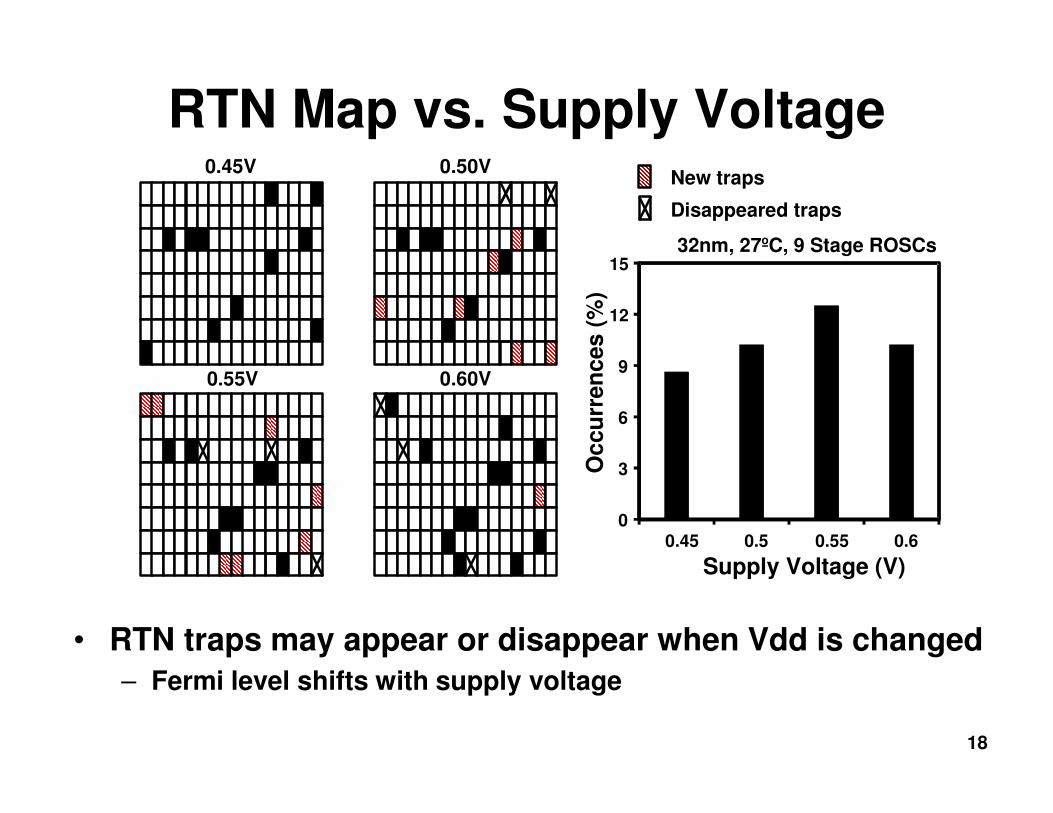
RTN Map vs. Supply Voltage0.45V 0.50V
0.55V 0.60V
32nm, 27ºC, 9 Stage ROSCs
0
3
6
9
12
15
0.45 0.5 0.55 0.6
Oc
cu
rren
ces
(%
)
Supply Voltage (V)
Disappeared traps
New traps
• RTN traps may appear or disappear when Vdd is changed
– Fermi level shifts with supply voltage
19
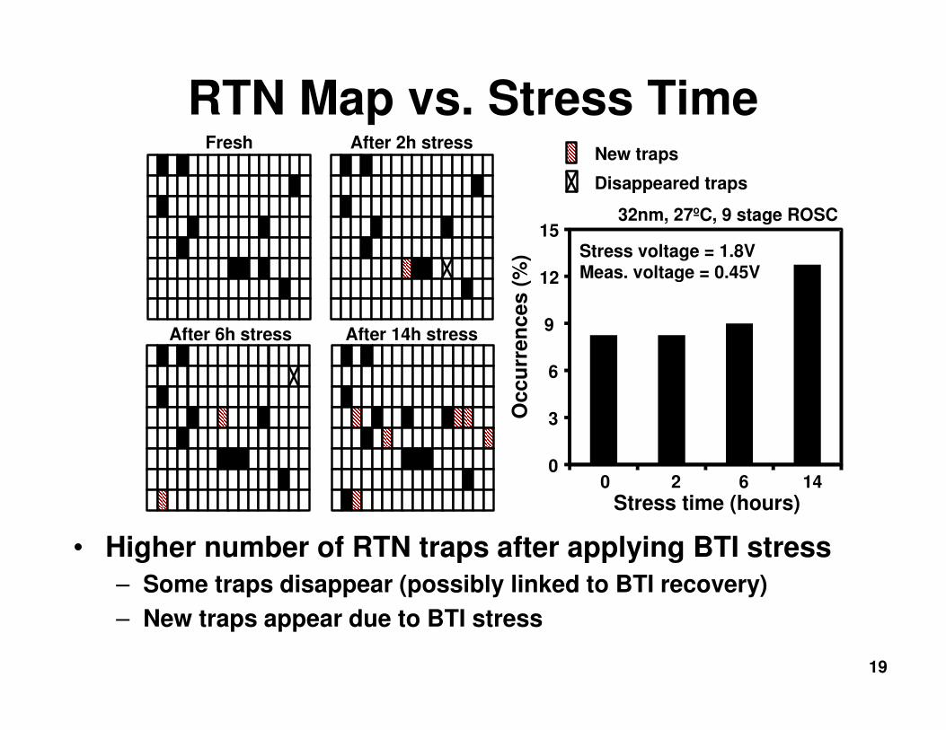
RTN Map vs. Stress Time
Occu
rren
ces (
%)
Fresh After 2h stress
0
3
6
9
12
15
0 2 6 14
Stress time (hours)
32nm, 27ºC, 9 stage ROSC
Stress voltage = 1.8VMeas. voltage = 0.45V
After 6h stress After 14h stress
Disappeared traps
New traps
• Higher number of RTN traps after applying BTI stress
– Some traps disappear (possibly linked to BTI recovery)
– New traps appear due to BTI stress
20
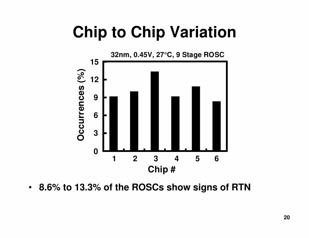
Chip to Chip Variation
0
3
6
9
12
15
1 2 3 4 5
Oc
cu
rren
ce
s (
%)
Chip #
6
32nm, 0.45V, 27°C, 9 Stage ROSC
• 8.6% to 13.3% of the ROSCs show signs of RTN
21
Outline of Presentation
• RTN Impact on Logic Timing
• Proposed Dual Ring Oscillator Array RTN Monitor
• 32nm Test Chip Results
• Timing Margin Analysis
• Conclusions
22
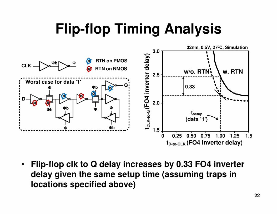
Flip-flop Timing Analysis
w/o. RTN w. RTN
tD-to-CLK (FO4 inverter delay)t C
LK
-to
-Q (F
O4
in
ve
rter
de
lay
)
32nm, 0.5V, 27ºC, Simulation
01.5
2.0
2.5
3.0
0.750.500.25 1.51.251.00
tsetup
(data '1')
0.33
D
QΦ
Φb Φb
Φ
Φb
Φ Φ
Φb
Worst case for data '1'
Φb CLK
Φ RTN on PMOS
RTN on NMOS
• Flip-flop clk to Q delay increases by 0.33 FO4 inverter delay given the same setup time (assuming traps in locations specified above)
23
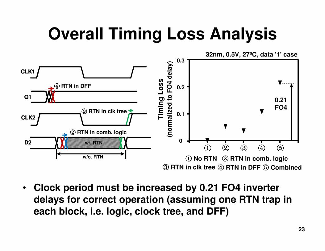
Overall Timing Loss Analysis
Tim
ing
Lo
ss
(no
rmalized
to
FO
4 d
ela
y)
①①①① No RTN ②②②② RTN in comb. logic
③③③③ RTN in clk tree ④④④④ RTN in DFF ⑤⑤⑤⑤ Combined
①①①① ②②②② ③③③③ ④④④④ ⑤⑤⑤⑤
32nm, 0.5V, 27ºC, data '1' case0.3
0.2
0.1
0
0.21 FO4
• Clock period must be increased by 0.21 FO4 inverter delays for correct operation (assuming one RTN trap in each block, i.e. logic, clock tree, and DFF)
CLK1
Q1
D2
CLK2
④④④④ RTN in DFF
③③③③ RTN in clk tree
CLK1
Q1
D2
CLK2
②②②② RTN in comb. logic
w/. RTN
w/o. RTN
24
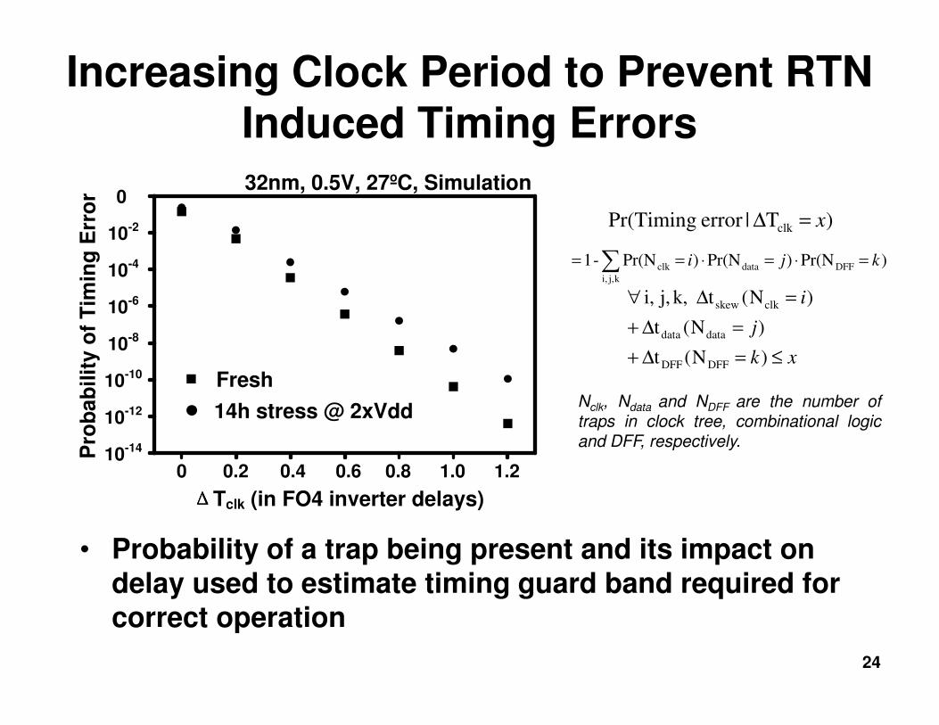
Increasing Clock Period to Prevent RTN Induced Timing Errors
10-14
10-12
10-10
10-8
10-6
10-4
10-2
0
0 0.2 0.4 0.6 0.8 1.0 1.2
Fresh
14h stress @ 2xVdd
ΔΔΔΔTclk (in FO4 inverter delays)
32nm, 0.5V, 27ºC, Simulation
Pro
bab
ilit
y o
f T
imin
g E
rro
r
) T |error Pr(Timing clk x=∆
) Pr(N) Pr(N) Pr(N -1 DFFdata
kj,i,
clk kji =⋅=⋅== ∑
xk
j
i
≤=∆+
=∆+
=∆∀
)N(t
)N(t
)N(t k,j, i,
DFFDFF
datadata
clkskew
Nclk, Ndata and NDFF are the number oftraps in clock tree, combinational logicand DFF, respectively.
• Probability of a trap being present and its impact on delay used to estimate timing guard band required for correct operation
Conclusions• New dual ROSC array can measure RTN induced
frequency shift with resolution <0.01% at 0.45V
• Various aspects of RTN measured from a 32nm test chip
• Assessed RTN impact on logic path timing and estimated probability of timing error
25
AcknowledgementThis work was supported in part by the Failure-Resistant Systems (FRS) program, a joint initiativebetween the National Science Foundation (NSF) andthe Semiconductor Research Corporation (SRC).