Embed Size (px)
Citation preview

ASIC TesterAlfred Gifford, Ruben Gottardi, Daniel Khoury, Tyler Martinsen
University of UtahSalt Lake City, UT 84102
Abstract—Our senior project is an ASIC tester meant to testchips that students in CS/ECE 5710 (or 6710) fabricate. Theultimate goal of this project to mimic and replace the Universityof Utah’s LV500, a Tektronix logic verifier from 1989, which hasfailing parts and requires difficult-to-find replacement parts. Ourproject lacks some advanced features seen on the LV500, suchas current limitation, schmooing, FTP support, but successfullyreplicates much of the logic verifier’s core functionality.
I. INTRODUCTION AND MOTIVATION
At the University of Utah, students enrolled in CS/ECE5710 (or 6710) design an integrated circuit (IC) for their finalproject and have the option of letting MOSIS, an IC foundry,fabricate their chip. After fabrication, as per MOSIS’s rules,students are required to test their chips and report their resultsback to MOSIS. CS/ECE 6712 teaches students how to testtheir chips using a device called an ASIC tester.
Presently, the University of Utah has two ASIC testers: aVerigy 93000 and an LV500. At the time that we proposedour project, the Verigy 93000 was seen as a very difficultmachine to use, with several functionality issues plaguing itsuse. The LV500 is simpler to use and has been used in the pastby students to test their fabricated chips, but the machine isover 20 years old; parts of the machine are failing, and findingreplacement parts is becoming increasingly difficult with time.
ASIC testers are generally very expensive (usually aroundmillions of dollars), and the chips that students test usuallydo not require the level of functionality provided by suchexpensive machines. Rather than require the University ofUtah to continually hunt down obscure replacement parts orspend money on a new ASIC tester, we proposed to constructa low-cost ASIC tester design based primarily upon an FPGAboard and a phase-locked loop (PLL) module.
(As of this writing, the Verigy 93000 appears to be veryclose to operational. However, there is still considerable inter-est among some individuals in having our project available asa substitute.)
II. BACKGROUND
ASIC testers are machines that allow users to send electricalsignals to a chip, sample output signals from that chip, andverify whether the signals match their expectations or not. Thissection primarily reviews the operation of the LV500-seriesASIC testers, whose functionality we attempted to mimic inour project. In the LV500, timing waveforms (which can bethought of as internal clock signals) are configured by theuser and are used to coordinate when signals are sent toand sampled from a chip. Figure 1 illustrates a so-called
test cycle. Signals are sent to a chip at the rising edge ofa timing waveform and sampled from the chip at the fallingedge of the timing waveform. Multiple test cycles can be usedconcurrently to send inputs and sample outputs at differenttimes but within the scope of a single test cycle period, asshown in Figure 2. Other important aspects of the LV500sfunctionality include:
* The ability to parse an external test file.* Schmooing, where a chip is tested under varying electri-cal conditions (for instance, 4.3V is chosen to representa 1 instead of 5.0V).
* A GUI allowing users to run tests.
Fig. 1. LV500 timing definitions.
Fig. 2. Testing an AND gate using the LV500.
III. PROJECT IMPLEMENTATION
The system as a whole can be divided into three sections:* The main PCB, used for housing the ASIC.* The FPGA systems that work to generate timing wave-forms and initiate tests.

* The software used to interface with the rest of thesystem.Two parts that we used and are mentioned throughout theremainder of this paper are the Numato Saturn Spartan-6 FPGA Development Board (see Figure 3) and theDigilent Atlys board (see www.digilentinc.com/atlys/ fordetails). Figure 4 below shows a hardware flow diagramrepresenting our project.
Fig. 3. Numato board.
Fig. 4. Hardware flow diagram.
A. Main PCB
A fundamental part of our project is being able to easilyconnect a MOSIS-fabricated chip. The main PCB’s purposeis to provide housing for these chips. We defined our require-ments as:
* The ability to access a large number of I/O pins.* The ability to use any pin as an input, output, power
connection, and ground connection.* Voltage leveling between the Numato board (whichoperates on 3.3V) and the chip under test, which operateson 5V.
1) Pin Count: The first requirement listed was constrainedby the number of I/O pins on the Numato board. The Numatogave us access to 150 pins. The largest MOSIS-packaged chipthat we could support consists of 139 pins, so we devoted 139Numato pins to the main PCB and the remaining 11 pins forSPI communication.
2) PCB Design: Using jumpers and jumper wires, theuser has the ability to manually wire power and ground anddetermine whether they wish to have an ASIC pin float or beconfigured to an input or output. Additionally, the user canroute power out to an external adjustable voltage regulator
if they wish to schmoo manually. The final PCB is shownin the image at the following page: http://www.eng.utah.edu/∼dkhoury/main pcb.jpg
3) Voltage Leveling: Figure 5 below shows the schematicof the voltage leveler we ultimately used.
Fig. 5. Voltage leveler. Schematic from http://dlnmh9ip6v2uc.cloudfront.net/datasheets/BreakoutBoards/Logic Level Bidirectional.pdf.
B. FPGA: Verilog, MicroBlaze
We use a Spartan-6 FPGA to generate timing waveformsand house all of the logic required to send and sample bitsto/from the ASIC at appropriate times. As a whole, the FPGAis configured as a SPI slave. The image at the following pageillustrates the circuits implemented onto the board (sans thefinite state machines used for control signals): http://www.eng.utah.edu/∼dkhoury/verilog.png
A phase-locked loop (PLL) built into the FPGA is used togenerate the timing waveforms. The PLL is a powerful pieceof hardware, able to perform the following functions:
* Multiplying clocks.* Dividing clocks.* Allowing the frequencies, phase shifts, and duty cyclesof the output clocks to be dynamically reprogrammed.(See here: http://www.xilinx.com/support/documentation/application notes/xapp879.pdf.)
The dynamic reprogrammability is especially important.One general goal with major projects like ours is to leave theuser of the system with as minimal work to do as possible.Hence, it’s best if the timing waveforms are dynamicallyreconfigurable so that the user does not have to resynthesizethe Verilog onto the FPGA for their specific needs, but caninstead specify their desired configuration state through moreabstracted methods.
Due to routing issues, we could not feed the 100 MHz clocksignal on the Numato board directly into the PLL; we had touse a digital clock manager (DCM) as effectively a buffer.Routing issues also led us to output no more than two clocksignals from the PLL.
We configured the PLL to output all clock signals at 2MHz, with duty cycles fixed at 50 percent. (See the ’Pitfalls
and Discoveries’ section for our justification of this designchoice.) One clock signal is designated as the ”DATA” timingwaveform and the other clock signal is designated as the”CLOCK” timing waveform. When testing a combinationalchip, such as an inverter, the user is expected to only usethe DATA waveform. When testing a sequential chip, suchas a register, the user is expected to use both the DATA andCLOCK signals, and can specify the phase difference betweenthe DATA and CLOCK signals (either 45, 90, or 135 degrees).Output bits are always sampled on the falling edge of theDATA waveform.
The FPGA accepts six one-hot chip select (CS) lines,allowing it to retrieve the following test information (note thatthe last three bullet points are only relevant for pins configuredto be inputs to the ASIC):
* A PLL reconfiguration state. This data must only besent if the user is testing a chip that requires two timingwaveforms.
* Which pins are inputs and which pins are outputs.* A signal to initiate a test cycle.* The bits to be sent to the ASIC.* The force format for each pin. We implemented all ofthe force formats that the LV500 supports except for RIH.
* The timing waveform (DATA or CLOCK) that each pinadheres to.
The image at this webpage (http://www.eng.utah.edu/∼dkhoury/fsms.png) shows the finite state machines (FSMs)that exist in the Verilog. There are two reset signals: oneto reset the DCM, and one labeled as ’GLOBAL RST’. AnFSM is required for the reset logic due to the asynchronousnature of the entire design. Otherwise, the design is not overlycomplicated. Generally, we wait for a SPI message and thendecode it. If the SPI message instructs us to reconfigure thePLL, we trigger a FSM that does so. If the SPI messageinstructs us to initiate the test, through careful timing, we pushall of the clocked-in bits through the double-buffered registers,allow the PLL clocks to run (they are normally blocked by theBUFGMUX modules) for about 500 nanoseconds, and thenhalt the test. The TEST WAIT period ensures that we don’trun two tests in a row, in case the corresponding CS line isheld down for longer than anticipated.
To provide easy pin access to the Numato board, we createda shield for it. The schematic for this shield is availablehere (http://www.eng.utah.edu/∼dkhoury/pcb boards/FPGAShield.PDF) and the layout is available here (http://www.eng.utah.edu/∼dkhoury/pcb boards/fpga shield layout.PNG).
The MicroBlaze code implemented onto the Atlys board is,in essence, a SPI-to-serial and serial-to-SPI converter. Usingthe XPS SPI drivers provided by Xilinx, the MicroBlaze code’ssole purpose is to extract serial messages from a PC (whereinthe messages contain testing information), send analogous SPImessages to the Numato board, retrieve test results from theNumato board, and convert the test results into serial messagessend over the COM port.
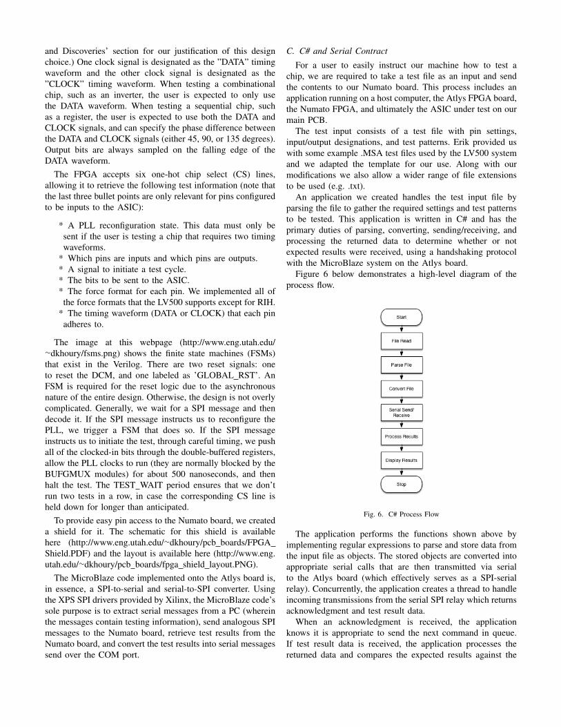
C. C# and Serial Contract
For a user to easily instruct our machine how to test achip, we are required to take a test file as an input and sendthe contents to our Numato board. This process includes anapplication running on a host computer, the Atlys FPGA board,the Numato FPGA, and ultimately the ASIC under test on ourmain PCB.
The test input consists of a test file with pin settings,input/output designations, and test patterns. Erik provided uswith some example .MSA test files used by the LV500 systemand we adapted the template for our use. Along with ourmodifications we also allow a wider range of file extensionsto be used (e.g. .txt).
An application we created handles the test input file byparsing the file to gather the required settings and test patternsto be tested. This application is written in C# and has theprimary duties of parsing, converting, sending/receiving, andprocessing the returned data to determine whether or notexpected results were received, using a handshaking protocolwith the MicroBlaze system on the Atlys board.
Figure 6 below demonstrates a high-level diagram of theprocess flow.
Fig. 6. C# Process Flow
The application performs the functions shown above byimplementing regular expressions to parse and store data fromthe input file as objects. The stored objects are converted intoappropriate serial calls that are then transmitted via serialto the Atlys board (which effectively serves as a SPI-serialrelay). Concurrently, the application creates a thread to handleincoming transmissions from the serial SPI relay which returnsacknowledgment and test result data.
When an acknowledgment is received, the applicationknows it is appropriate to send the next command in queue.If test result data is received, the application processes thereturned data and compares the expected results against the

received results, informing the user of which bits came backas expected and which bits did not.
Figure 7 below shows our GUI used to test a D flip-flop.The user specifies which COM port the MicroBlaze systemis connected to, uploads a test file, and the back-end codeworks to execute the test. The results are promptly displayedto the user on the terminal-like screen shown in the image.Bits that were sampled incorrectly are shown in red text. (Alarger picture of this image can be seen here: http://www.eng.utah.edu/∼dkhoury/colored bits.PNG.)
Fig. 7. C# GUI.
D. Demo Chip
Because our project lacks actuators and any kind of lightart, we had to consider two audiences when demoing ourproject: individuals familiar with electronics and individualsunfamiliar with electronics. We decided it would be optimaldemonstrate at least one simple sequential circuit to the formeraudience and at least one simple combinational circuit to thelatter audience.
MOSIS held an educational fabrication run in June 2014,and we took advantage of this opportunity by fabricating adigital chip with the following circuits:
* Inverter.* AND gate.* OR gate.* 4-bit adder.* 2-bit multiplier.* 2-bit decoder.* 4-bit encoder.* 4-bit binary up-counter.* 4-bit shift register.* 1-bit D flip-flop.* 4-bit ring counter.
Ultimately, in our demonstration, we demoed the inverter,AND gate, and OR gate to everybody, and the D flip-flop topeople familiar with electronics.
E. Design Process
1) Main PCB: We initially assumed designing the mainPCB would be trivial; surprisingly, that was not the case. Themain PCB was in fact fabricated three different times. Thefirst design had several problems. The most prominent issue
was that the drill holes for the ZIF socket were too small.When designing the board in Altium, we used the datasheetfor the socket to specify our hole sizes but we neglected totake into account the effect of the plating on the hole sizes.There were also some other errors (shorts between pins dueto copy-and-paste errors) which would have made this boardnearly unusable and very hard to debug. In the second run,we fixed the aforementioned issues and made some additions,including heavy use of silkscreen and power-indicating LEDs.After we received this board, we soldered all componentsonto the board and tested the circuit. It quickly became clearthat the board was malfunctioning, which we later learnedwas due to swapping two pins on our voltage translators.By the time we decided to fabricate a third PCB, we werethree weeks away from our demo date. For this reason,we decided to plaster onto the main PCB several breakoutboards from Sparkfun that contain the voltage translatingcircuit. The final schematic be seen here (http://www.eng.utah.edu/∼dkhoury/pcb boards/ASIC Sch.PDF) and the finallayout can be seen here (http://www.eng.utah.edu/∼dkhoury/pcb boards/main pcb layout.PNG).
2) PLL: We initially proposed to create an ASIC tester withboth functionality testing and timing testing. In the latter case,the idea is to see how quickly we can sample output bits froma chip after sending input bits to the chip before the sampledbits become incorrect in value. We believed the Spartan-6’sPLL could achieve this goal for us, but testing the PLL provedotherwise for the following reasons:
* The PLL appeared to have major stability problems atall frequencies except for 2 MHz. Even at 2 MHz, theclock signals sometimes exhibit some jitter.
* The PLL will not necessarily produce the exact fre-quency, phase shift, and duty cycle programmed into it.Because of the way in which the PLL prioritizes certainparameters over others, specifying a frequency of 5 MHz,37 degree phase shift, and 30 percent duty cycle mightproduce a clock with 5 MHz frequency, 45 degree phaseshift, and 30 percent duty cycle.
Due to these issues, we reframed our project to serve only asa functionality tester.
3) Software Interfacing: The initial conception of ourproject was to have a keyboard-driven UI running on aNumato FPGA board. The Numato board would then send,receive, and process the data from our main PCB board todetermine and present the test results to the user. Due tochallenges and hardware limitations described in Appendix A:Pitfalls and Discoveries, we were forced to adapt and modifyour original direction (the final product satisfied virtually allof our original objectives, but the path was very differentthan anticipated). Design changes forced our application tobe written for and executed on a PC system. This changepresented fewer hardware limitations and a wider array ofsoftware libraries. By moving our application to a host PC theFPGA board was then used primarily for a serial-SPI relay.

IV. EVALUATION
The main PCB fulfilled its primary duty of providinghousing to a MOSIS chip and supporting voltage leveling.Multimeter tests never revealed any issues with the main PCB,though we were unable to directly incorporate the followingbonus features: *
* Schmooing abilities. (Our compromise was to providethe user with the option to send the power from the barrel-type power jack source to an external adjustable regulator,for what is basically manual schmooing.)
* Equalized trace lengths, which would have allowed usto provide the user with an estimate of the delay timebetween the Numato board and the ASIC. We attemptedto use Altium’s tools to equalize trace lengths, but thetools could only bring the traces within four to sixinches of each other. (Indeed, equalized trace lengths isa surprisingly hard problem.) Since we rebranded ourproject as a functional tester, this bonus feature becameunimportant. If users wish, they can hook up a logicanalyzer to the jumpers surrounding the ZIF socket andget a rough approximation of their chip’s performance.
The PLL proved to be less versatile than we had hopedfor. The Verilog as a whole is able to do everything that weintended it to do, save for the lack of timing options imposedby the PLL’s functional constraints. An ideal PLL would haveallowed us to specify any frequency, phase shift, and dutycycle for the output clocks. In the end, we were happy thatwe were able to make any use of it!
The initial intent for the software side of our project wasto have a GUI which would allow users to enter and changethe tests we would perform via a keyboard. This GUI wouldideally have allowed a user to save those tests (a feature wewere considering implementing if we had time). However,because we ended up moving the GUI from the MicroBlazesystem to a computer program written in C# (which can be runon any Windows system), we were able to take advantage ofa PC’s offerings (like saving files). We subsequently decidedto focus more on loading saved tests versus developing testsin a GUI, which is generally infeasible for users to do due tothe complexity of many test files. This way, a user can writea test in an MSA file with their favored IDE and not haveto deal with any possible disconnects or incapabilities a GUImay provide.
The more straightfoward GUI we developed now providesa clean interface which allows a user to select the COM portthey are using and the file they want to test. After selectingthe file the tests are executed and the user is presented withthe results formatted according to the patterns section of theircode with the term ’Pass’ or ’Fail’ appended. Should a testfail, the user is also presented with the output bits that failedhighlighted in red to help clarify where the error may exist.As of now, the test file only supports one template (in LV500-speak) – we plan to include support for multiple templates inthe future.
As a whole, the project appears to work (in that a chip canbe correctly tested, when using a machine like the LV500 forreference), though we’ve only tested simple circuits so far. Wedo plan to test the project further with the more complicatedcircuits on the demo chip (e.g. binary up-counter).
V. CONCLUSIONS
As simple as the idea of a logic verifier is, the many detailsbehind its implementation make it a challenging project toimplement. It’s especially incredible to think that even withthe technology of 2014, it’s no trivial task to mimic a machinecreated 25 years earlier! We are proud that we were able tocreate an ASIC tester that, at the very least, can test relativelysimple chips (further testing will show whether it can test morecomplicated chips). We accomplished most of our proposedgoals and learned much along the way. For reference, Figure8 below shows the current project as it stands. We plan to
Fig. 8. Current system. Shown is the main PCB, the FPGA shield createdfor the Numato board, the MicroBlaze system (Atlys board), and a PC to thevery far right.
continue working on this project, as we are determined to atleast provide a substitute tester for students in CS/ECE 6712.Additional work includes:
* More versatility in the test files (e.g. multiple templatesupport).
* Further testing to provide confidence in the machine.* Finishing up documentation on how the system as awhole works.
* (Ideally) the ability to convert a PDF of a bondingdiagram into the majority contents of a test file usingan image-processing program.
Our website is located at http://atr.eng.utah.edu/∼gottardi/MixedSignals/index.php. Note that pitfalls and discoveries isalso mentioned on the ’Project Results’ page.
ACKNOWLEDGMENT
We are thankful for all of the individuals that provided uswith help throughout the course of this semester. In particular,we’d like to thank the following people:
* Brent Mellor, who allowed us to use his workplace’sreflow oven.

* Erik Brunvand, who provided us with parts and guidancethroughout the project.
* Anh Luong and Mike Empey, who helped us create astencil for our main PCB.
* Travis Stroud, who provided us ribbon cables.* Our families, who put up with our absences and willnow need to get to know us again.
APPENDICES
A. Appendix A: Pitfalls and Discoveries
1) Numato did not provide any *.bsb files for the boardwe purchased. This made it virtually impossible to flashany MicroBlaze code to the board. We attempted to workwith Numato on this issue but their technical support wasless than helpful. In response, we moved the MicroBlazeportion of the code to an Atlys board that Erik Brunvandprovided us.
2) We initially began development for the software side inJava. We had already written a parser when we attemptedto add a serial connection in our code. This led to theharsh discovery that Java, being run in a virtual sandbox,does not play well with COM ports. After weeks oftroubleshooting we abandoned Java and moved over toC# which provided a better connection to the COM portsand required significantly less code.
3) The initial voltage translators that we purchased andtested (part number TXB0108) ”autodetect” the direc-tion of voltage propagation by using extremely weakinternal drivers to drive voltages. Others should use thisparticular device with caution due to its poor drivingcapabilities.
4) It is hard to get even simple PCB designs correct onthe first try. With the first version of our main PCB,we didn’t account for how plating would affect holesizes. On the first revision, we accidentally created ashort between two pins due to a copy-and-paste error.Not until the second revision did our board work to oursatisfaction.
5) The drain and source of a MOSFET are NOT inter-changeable due to a parasitic diode (technically a zenerdiode but can generally be thought of as a unidirectionaldiode) that lies between those two terminals. The firstrevision of our main PCB failed because we mixedup the source and drain locations on the MOSFETswe used. For more information on this topic, one canresearch ”source-drain diode.” In general, MOSFETsshould be handled as follows: ** Of the voltages applied to the source, drain, and
body, the source should be tied to the lowest voltage(NMOS) or the highest voltage (PMOS).
* The drain and source of a MOSFET are not necessar-ily interchangeable, whether the application is analogor digital.
6) The PLL code provided by Xilinx refused to implementonto the Spartan-6 FPGA on the Numato board. (The
code synthesized but an odd error related to the locationof the clock signal on the Numato board prevented thecode from mapping successfully onto the hardware.)Several attempts to resolve the bug, including seekinghelp on the Xilinx forum and emailing the author ofthe PLL code for assistance, failed to bring about aresolution. As a desperation measure, we attempted to tiethe output of a DCM to the PLL – with a few tweaks, wemanaged to get the PLL to implement onto the FPGA.
B. Appendix B: Bill of Materials
The Bill of Materials (BOM.pdf) can be found at http://www.eng.utah.edu/∼dkhoury/BOM.pdf.
C. Appendix C: Schematics and Code
All schematics and code can be found at http://www.eng.utah.edu/∼dkhoury/.