Embed Size (px)
Citation preview
www.ams.com Revision 1.1 / 10.07.2013 page 1/11
User Manual – AS5311 – AB – 1.1
AS5311
12-bit Linear Incremental Position Sensor with ABI and
PWM output

User Manual – AS5311 – AB – 1.1
www.ams.com Revision 1.1 / 10.07.2013 page 2/11
Table of Contents
1 General Description.............................................................................................................. 3
2 The AS5311 adapter board .................................................................................................. 4
2.1 Board description ................................................................................................................. 4
2.2 Mounting the AS5311 adapter board ................................................................................... 4
3 AS5311 adapter board and pinout ....................................................................................... 6
4 Operation .............................................................................................................................. 7
4.1 Standalone PWM output mode ............................................................................................ 7
5 Using the serial interface with MCU ..................................................................................... 8
5.1 3-wire serial interface ........................................................................................................... 8
6 AS5311 adapterboard hardware ........................................................................................ 10
6.1 AS5311-AB-1.1 schematics ............................................................................................... 10
6.2 AS5311-AB-1.1 PCB Layout .............................................................................................. 10
7 Copyright ............................................................................................................................ 11
8 Disclaimer ........................................................................................................................... 11
9 Contact Information ............................................................................................................ 11
Revision History
Revision Date Owner Description
1.0 01.10.2009 Initial revision
1.1 10.07.2013 azen Updated to new template + minor corrections
User Manual – AS5311 – AB – 1.1
www.ams.com Revision 1.1 / 10.07.2013 page 3/11
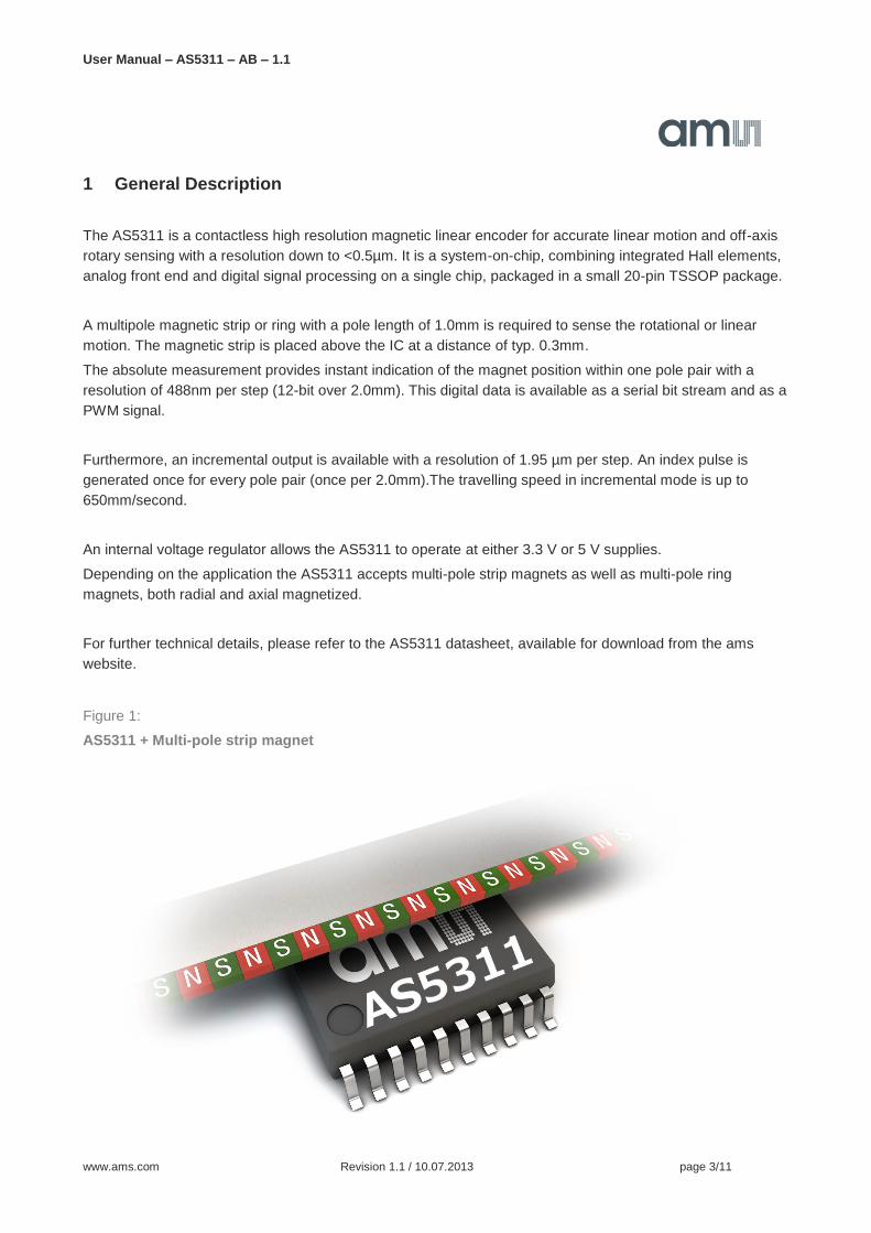
1 General Description
The AS5311 is a contactless high resolution magnetic linear encoder for accurate linear motion and off-axis
rotary sensing with a resolution down to <0.5µm. It is a system-on-chip, combining integrated Hall elements,
analog front end and digital signal processing on a single chip, packaged in a small 20-pin TSSOP package.
A multipole magnetic strip or ring with a pole length of 1.0mm is required to sense the rotational or linear
motion. The magnetic strip is placed above the IC at a distance of typ. 0.3mm.
The absolute measurement provides instant indication of the magnet position within one pole pair with a
resolution of 488nm per step (12-bit over 2.0mm). This digital data is available as a serial bit stream and as a
PWM signal.
Furthermore, an incremental output is available with a resolution of 1.95 µm per step. An index pulse is
generated once for every pole pair (once per 2.0mm).The travelling speed in incremental mode is up to
650mm/second.
An internal voltage regulator allows the AS5311 to operate at either 3.3 V or 5 V supplies.
Depending on the application the AS5311 accepts multi-pole strip magnets as well as multi-pole ring
magnets, both radial and axial magnetized.
For further technical details, please refer to the AS5311 datasheet, available for download from the ams
website.
Figure 1:
AS5311 + Multi-pole strip magnet
User Manual – AS5311 – AB – 1.1
www.ams.com Revision 1.1 / 10.07.2013 page 4/11
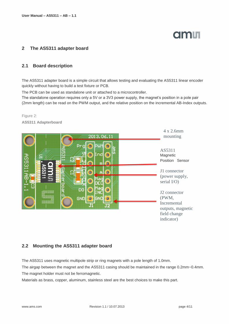
2 The AS5311 adapter board
2.1 Board description
The AS5311 adapter board is a simple circuit that allows testing and evaluating the AS5311 linear encoder
quickly without having to build a test fixture or PCB.
The PCB can be used as standalone unit or attached to a microcontroller.
The standalone operation requires only a 5V or a 3V3 power supply, the magnet’s position in a pole pair
(2mm length) can be read on the PWM output, and the relative position on the incremental AB-Index outputs.
Figure 2:
AS5311 Adapterboard
2.2 Mounting the AS5311 adapter board
The AS5311 uses magnetic multipole strip or ring magnets with a pole length of 1.0mm.
The airgap between the magnet and the AS5311 casing should be maintained in the range 0.2mm~0.4mm.
The magnet holder must not be ferromagnetic.
Materials as brass, copper, aluminum, stainless steel are the best choices to make this part.
AS5311 Magnetic
Position Sensor
4 x 2.6mm
mounting
holes
J1 connector
(power supply,
serial I/O)
J2 connector
(PWM,
Incremental
outputs, magnetic
field change
indicator)

User Manual – AS5311 – AB – 1.1
www.ams.com Revision 1.1 / 10.07.2013 page 5/11
Figure 3:
AS5311 adapter board mounting and dimension
AS53110.2~0.4mm
AS5311
J1
J2
GN
D
PW
M
Ind
B A
Ma
g
Inc
GN
D
Prg
5V
3V
3
CS
n
CL
K
DO
Ma
g
De
c
18mm
11
mm
28
mm
22mm
4x2.6mm
N SN S N NS S
0.6
2m
m
User Manual – AS5311 – AB – 1.1
www.ams.com Revision 1.1 / 10.07.2013 page 6/11
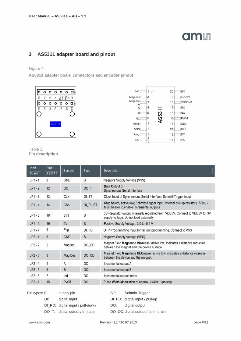
3 AS5311 adapter board and pinout
Figure 4:
AS5311 adapter board connectors and encoder pinout
AS5311
J1
J2
GN
D
PW
M
Ind
B A
Ma
g
Inc
GN
D
Prg
5V
3V
3
CS
n
CL
K
DO
Ma
g
De
c
Table 1: Pin description
Pin#
Board
Pin#
AS5311 Symbol Type Description
JP1 - 1 8 GND S Negative Supply Voltage (VSS)
JP1 - 2 12 DO DO_T Data Output of Synchronous Serial Interface
JP1 - 3 13 CLK DI, ST Clock Input of Synchronous Serial Interface; Schmitt-Trigger input
JP1 - 4 14 CSn DI_PU,ST Chip Select, active low; Schmitt-Trigger input, internal pull-up resistor (~50k). Must be low to enable incremental outputs
JP1 - 5 18 3V3 S 3V-Regulator output; internally regulated from VDD5V. Connect to VDD5V for 3V supply voltage. Do not load externally.
JP1 - 6 19 5V S Positive Supply Voltage, 3.0 to 5.5 V
JP1 - 7 9 Prg DI_PD OTP Programming Input for factory programming. Connect to VSS
JP2 - 1 8 GND S Negative Supply Voltage (VSS)
JP2 - 2 2 Mag Inc DO_OD Magnet Field Magnitude INCrease; active low, indicates a distance reduction between the magnet and the device surface
JP2 - 3 3 Mag Dec DO_OD Magnet Field Magnitude DECrease; active low, indicates a distance increase between the device and the magnet.
JP2 - 4 4 A DO Incremental output A
JP2 - 5 5 B DO Incremental output B
JP2 - 6 7 Ind DO Incremental output Index.
JP2 - 7 15 PWM DO Pulse Width Modulation of approx. 244Hz; 1µs/step
2
3
4
5
6
7
8 13
14
15
16
17
18
19
201NC
MagIncn
MagDec
n
A
B
NC
Index
VSS CLK
CSn
PWM
NC
NC
VDD3V3
VDD5V
AS
53
11
9 12 DOProg
1
011 NCNC
NC
Pin types: S: supply pin ST: Schmitt-Trigger
DI: digital input DI_PU: digital input / pull-up
DI_PD: digital input / pull-down DO: digital output
DO_T: digital output / tri-state DO_OD: digital output / open drain
User Manual – AS5311 – AB – 1.1
www.ams.com Revision 1.1 / 10.07.2013 page 7/11
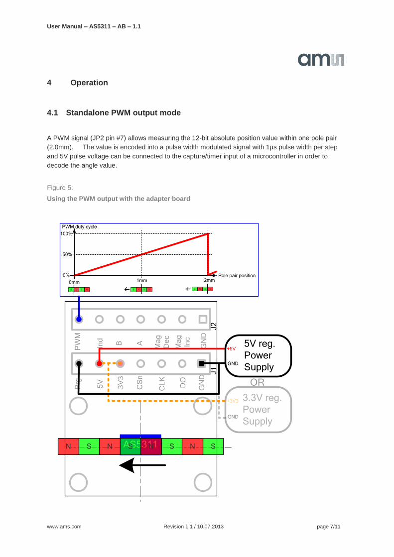
4 Operation
4.1 Standalone PWM output mode
A PWM signal (JP2 pin #7) allows measuring the 12-bit absolute position value within one pole pair
(2.0mm). The value is encoded into a pulse width modulated signal with 1µs pulse width per step
and 5V pulse voltage can be connected to the capture/timer input of a microcontroller in order to
decode the angle value.
Figure 5:
Using the PWM output with the adapter board
AS5311
J1
J2
GN
D
PW
M
Ind
B A
Ma
g
Inc
GN
D
Prg
5V
3V
3
CS
n
CL
K
DO
Ma
g
De
c
0mm 2mm1mm0%
100%
50%
PWM duty cycle
Pole pair position
5V reg.
Power
Supply
+5V
GND
+3V3
GND
3.3V reg.
Power
Supply
NSNS NSNS NSNS
N SNSNSNS
OR

User Manual – AS5311 – AB – 1.1
www.ams.com Revision 1.1 / 10.07.2013 page 8/11
The absolute serial output counts from 0….4095 within one pole pair a repeats with each subsequent
pole pair.
The PWM output starts with a pulse width of 1µs, increases the pulse width with every step of
0.488µm and reaches a maximum pulse width of 4097µs at the end of each pole pair. See AS5311
datasheet for more details on the PWM output.
The PWM frequency is internally trimmed to an accuracy of 5% (10% over full temperature range
Figure 6:
PWM duty cycle depending on magnet position
0V
5V
1µs
PWM
out
Absolute position
(12-bit value)Pos 0 Pos 4095
PWmin PWmax
4098µs 4097µs0µs 0µs
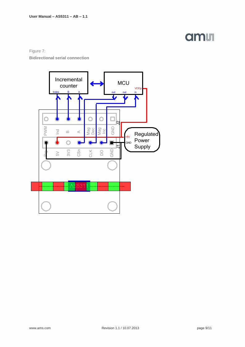
5 Using the serial interface with MCU
The most complete and accurate solution for a MCU to read the angle of a magnet is the serial
interface.
The 12 bit value of the angle will be directly read, and some other indicators as magnetic field strength
information or alarm bits can be read at the same time.
The connection between the MCU and the adapter board can be made with 3 wires.
5.1 3-wire serial interface
The Serial interface allows data transmission of the 12-bit absolute linear position information (within
one pole pair = 2.0mm). Data bits D11:D0 represent the position information with a resolution of
488nm (2000µm / 4096) per step.
CLK must be high at the falling edge of CSn.
If CLK is low at the falling edge of CSn, the first 12 bits represent the magnitude information, which is
proportional to the magnetic field strength.
User Manual – AS5311 – AB – 1.1
www.ams.com Revision 1.1 / 10.07.2013 page 9/11
Figure 7:
Bidirectional serial connection
AS5311
J1
J2
GN
D
PW
M
Ind
B A
Ma
g
Inc
GN
D
Prg
5V
3V
3
CS
n
CL
K
DO
Ma
g
De
c
Regulated
Power
Supply
+5V
GND
Incremental
counterMCU
VDDp
inIndex AB out out

User Manual – AS5311 – AB – 1.1
www.ams.com Revision 1.1 / 10.07.2013 page 10/11
6 AS5311 adapterboard hardware
Below the schematic and layout of the adapter board can be found.
6.1 AS5311-AB-1.1 schematics
Figure 8:
AS5311-AB-1.1 adapterboard schematics
6.2 AS5311-AB-1.1 PCB Layout
Figure 9:
AS5311-AB-1.1 adapter board layout
User Manual – AS5311 – AB – 1.1
www.ams.com Revision 1.1 / 10.07.2013 page 11/11
7 Copyright
Copyright ams AG, Tobelbader Strasse 30, 8141 Unterpremstätten, Austria-Europe. Trademarks
Registered. All rights reserved. The material herein may not be reproduced, adapted, merged,
translated, stored, or used without the prior written consent of the copyright owner.
8 Disclaimer
Devices sold by ams AG are covered by the warranty and patent indemnification provisions
appearing in its Term of Sale. ams AG makes no warranty, express, statutory, implied, or by
description regarding the information set forth herein. ams AG reserves the right to change
specifications and prices at any time and without notice. Therefore, prior to designing this product
into a system, it is necessary to check with ams AG for current information. This product is intended
for use in commercial applications. Applications requiring extended temperature range, unusual
environmental requirements, or high reliability applications, such as military, medical life-support or
life-sustaining equipment are specifically not recommended without additional processing by ams
AG for each application. This Product is provided by ams “AS IS” and any express or implied
warranties, including, but not limited to the implied warranties of merchantability and fitness for a
particular purpose are disclaimed.
ams AG shall not be liable to recipient or any third party for any damages, including but not limited
to personal injury, property damage, loss of profits, loss of use, interruption of business or indirect,
special, incidental or consequential damages, of any kind, in connection with or arising out of the
furnishing, performance or use of the technical data herein. No obligation or liability to recipient or
any third party shall arise or flow out of ams AG rendering of technical or other services.
9 Contact Information
Headquarters
ams AG
Tobelbader Strasse 30
8141 Unterpremstaetten
Austria
T. +43 (0) 3136 500 0
For Sales Offices, Distributors and Representatives, please visit:
http://www.ams.com/contact

Mouser Electronics
Authorized Distributor
Click to View Pricing, Inventory, Delivery & Lifecycle Information: ams:
AS5311-TS_EK_AB