Embed Size (px)
Citation preview

July 2009 Doc ID 13495 Rev 6 1/102
1
STR91xFAxxxARM966E-S™ 16/32-bit Flash MCU with Ethernet, USB, CAN,
AC motor control, 4 timers, ADC, RTC, DMA
Features 16/32-bit 96 MHz ARM9E based MCU
– ARM966E-S RISC core: Harvard archi-tecture, 5-stage pipeline, Tightly-Coupled Memories (SRAM and Flash)
– STR91xFA implementation of core adds high-speed burst Flash memory interface, instruction prefetch queue, branch cache
– Up to 96 MIPS directly from Flash memory– Single-cycle DSP instructions supported– Binary compatible with ARM7 code
Dual burst Flash memories, 32-bits wide– 256 KB/512 KB/1 MB/2 MB main Flash – 32 KB/128 KB secondary Flash– Sequential Burst operation up to 96 MHz– 100 K min erase cycles, 20 yr min retention
SRAM, 32-bits wide – 64K or 96K bytes, optional battery backup
9 programmable DMA channels
Clock, reset, and supply management– Internal oscillator operating with external
4-25 MHz crystal– Internal PLL up to 96 MHz – Real-time clock provides calendar
functions, tamper, and wake-up functions– Reset Supervisor monitors supply voltage,
watchdog, wake-up unit, external reset– Brown-out monitor– Run, Idle, and Sleep Mode as low as 50 uA
Vectored interrupt controller (VIC)– 32 IRQ vectors, 30 interrupt pins – Branch cache minimizes interrupt latency
8-channel, 10-bit A/D converter (ADC)– 0 to 3.6 V range, 0.7 usec conversion
10 Communication interfaces– 10/100 Ethernet MAC with DMA and MII – USB Full-speed (12 Mbps) slave device
– CAN interface (2.0B Active)– 3 16550-style UARTs with IrDA protocol – 2 Fast I2C™, 400 kHz– 2 channels for SPI™, SSI™, or
MICROWIRE™
External Memory Interface (EMI)– 8- or 16-bit data, up to 24-bit addressing– Static Async modes for LQFP128 – Additional burst synchronous modes for
LFBGA144
Up to 80 I/O pins (muxed with interfaces)
16-bit standard timers (TIM)– 4 timers each with 2 input capture, 2 output
compare, PWM and pulse count modes
3-Phase induction motor controller (IMC)
JTAG interface with boundary scan
Embedded trace module (ARM ETM9)
Table 1. Device summary
Reference Part number
STR91xFAx32STR910FAM32, STR910FAW32, STR910FAZ32, STR912FAW32
STR91xFAx42STR911FAM42, STR911FAW42, STR912FAW42, STR912FAZ42
STR91xFAx44STR911FAM44 STR911FAW44 STR912FAW44, STR912FAZ44
STR91xFAx46STR911FAM46, STR911FAW46,STR912FAW46, STR912FAZ46
STR91xFAx47STR911FAM47, STR911FAW47,STR912FAW47, STR912FAZ47
LQFP80 12 x12mm LQFP128 14 x 14mm
LFBGA144 10 x 10 x 1.7
www.st.com
Contents STR91xFAxxx
2/102 Doc ID 13495 Rev 6
Contents
1 Description . . . . . . . . . . . . . . . . . . . . . . . . . . . . . . . . . . . . . . . . . . . . . . . . 10
2 Device summary . . . . . . . . . . . . . . . . . . . . . . . . . . . . . . . . . . . . . . . . . . . 11
3 Functional overview . . . . . . . . . . . . . . . . . . . . . . . . . . . . . . . . . . . . . . . . 12
3.1 System-in-a-package (SiP) . . . . . . . . . . . . . . . . . . . . . . . . . . . . . . . . . . . 12
3.2 Package choice . . . . . . . . . . . . . . . . . . . . . . . . . . . . . . . . . . . . . . . . . . . . 12
3.3 ARM966E-S CPU core . . . . . . . . . . . . . . . . . . . . . . . . . . . . . . . . . . . . . . . 12
3.4 Burst Flash memory interface . . . . . . . . . . . . . . . . . . . . . . . . . . . . . . . . . 12
3.4.1 Pre-fetch queue (PFQ) . . . . . . . . . . . . . . . . . . . . . . . . . . . . . . . . . . . . . . 12
3.4.2 Branch cache (BC) . . . . . . . . . . . . . . . . . . . . . . . . . . . . . . . . . . . . . . . . 13
3.4.3 Management of literals . . . . . . . . . . . . . . . . . . . . . . . . . . . . . . . . . . . . . 13
3.5 SRAM (64 Kbytes or 96 Kbytes) . . . . . . . . . . . . . . . . . . . . . . . . . . . . . . . 15
3.5.1 Arbitration . . . . . . . . . . . . . . . . . . . . . . . . . . . . . . . . . . . . . . . . . . . . . . . 15
3.5.2 Battery backup . . . . . . . . . . . . . . . . . . . . . . . . . . . . . . . . . . . . . . . . . . . . 15
3.6 DMA data movement . . . . . . . . . . . . . . . . . . . . . . . . . . . . . . . . . . . . . . . . 15
3.7 Non-volatile memories . . . . . . . . . . . . . . . . . . . . . . . . . . . . . . . . . . . . . . . 16
3.7.1 Primary Flash memory . . . . . . . . . . . . . . . . . . . . . . . . . . . . . . . . . . . . . 16
3.7.2 Secondary Flash memory . . . . . . . . . . . . . . . . . . . . . . . . . . . . . . . . . . . 16
3.8 One-time-programmable (OTP) memory . . . . . . . . . . . . . . . . . . . . . . . . . 17
3.8.1 Product ID and revision level . . . . . . . . . . . . . . . . . . . . . . . . . . . . . . . . . 17
3.9 Vectored interrupt controller (VIC) . . . . . . . . . . . . . . . . . . . . . . . . . . . . . . 18
3.9.1 FIQ handling . . . . . . . . . . . . . . . . . . . . . . . . . . . . . . . . . . . . . . . . . . . . . 18
3.9.2 IRQ handling . . . . . . . . . . . . . . . . . . . . . . . . . . . . . . . . . . . . . . . . . . . . . 18
3.9.3 Interrupt sources . . . . . . . . . . . . . . . . . . . . . . . . . . . . . . . . . . . . . . . . . . 18
3.10 Clock control unit (CCU) . . . . . . . . . . . . . . . . . . . . . . . . . . . . . . . . . . . . . . 20
3.10.1 Master clock sources . . . . . . . . . . . . . . . . . . . . . . . . . . . . . . . . . . . . . . . 20
3.10.2 Reference clock (RCLK) . . . . . . . . . . . . . . . . . . . . . . . . . . . . . . . . . . . . 21
3.10.3 AHB clock (HCLK) . . . . . . . . . . . . . . . . . . . . . . . . . . . . . . . . . . . . . . . . . 21
3.10.4 APB clock (PCLK) . . . . . . . . . . . . . . . . . . . . . . . . . . . . . . . . . . . . . . . . . 21
3.10.5 Flash memory interface clock (FMICLK) . . . . . . . . . . . . . . . . . . . . . . . . 22
3.10.6 UART and SSP clock (BRCLK) . . . . . . . . . . . . . . . . . . . . . . . . . . . . . . . 22
3.10.7 External memory interface bus clock (BCLK) . . . . . . . . . . . . . . . . . . . . 22
STR91xFAxxx Contents
Doc ID 13495 Rev 6 3/102
3.10.8 USB interface clock . . . . . . . . . . . . . . . . . . . . . . . . . . . . . . . . . . . . . . . . 22
3.10.9 Ethernet MAC clock . . . . . . . . . . . . . . . . . . . . . . . . . . . . . . . . . . . . . . . . 22
3.10.10 External RTC calibration clock . . . . . . . . . . . . . . . . . . . . . . . . . . . . . . . . 22
3.10.11 Operation example . . . . . . . . . . . . . . . . . . . . . . . . . . . . . . . . . . . . . . . . . 23
3.11 Flexible power management . . . . . . . . . . . . . . . . . . . . . . . . . . . . . . . . . . 23
3.11.1 Run mode . . . . . . . . . . . . . . . . . . . . . . . . . . . . . . . . . . . . . . . . . . . . . . . 23
3.11.2 Idle mode . . . . . . . . . . . . . . . . . . . . . . . . . . . . . . . . . . . . . . . . . . . . . . . . 24
3.11.3 Sleep mode . . . . . . . . . . . . . . . . . . . . . . . . . . . . . . . . . . . . . . . . . . . . . . 24
3.12 Voltage supplies . . . . . . . . . . . . . . . . . . . . . . . . . . . . . . . . . . . . . . . . . . . . 24
3.12.1 Independent A/D converter supply and reference voltage . . . . . . . . . . . 24
3.12.2 Battery supply . . . . . . . . . . . . . . . . . . . . . . . . . . . . . . . . . . . . . . . . . . . . 25
3.13 System supervisor . . . . . . . . . . . . . . . . . . . . . . . . . . . . . . . . . . . . . . . . . . 25
3.13.1 Supply voltage brownout . . . . . . . . . . . . . . . . . . . . . . . . . . . . . . . . . . . . 25
3.13.2 Supply voltage dropout . . . . . . . . . . . . . . . . . . . . . . . . . . . . . . . . . . . . . 26
3.13.3 Watchdog timer . . . . . . . . . . . . . . . . . . . . . . . . . . . . . . . . . . . . . . . . . . . 26
3.13.4 External RESET_INn pin . . . . . . . . . . . . . . . . . . . . . . . . . . . . . . . . . . . . 26
3.13.5 Power-up . . . . . . . . . . . . . . . . . . . . . . . . . . . . . . . . . . . . . . . . . . . . . . . . 26
3.13.6 JTAG debug command . . . . . . . . . . . . . . . . . . . . . . . . . . . . . . . . . . . . . 26
3.13.7 Tamper detection . . . . . . . . . . . . . . . . . . . . . . . . . . . . . . . . . . . . . . . . . . 27
3.14 Real-time clock (RTC) . . . . . . . . . . . . . . . . . . . . . . . . . . . . . . . . . . . . . . . 27
3.15 JTAG interface . . . . . . . . . . . . . . . . . . . . . . . . . . . . . . . . . . . . . . . . . . . . . 27
3.15.1 In-system-programming . . . . . . . . . . . . . . . . . . . . . . . . . . . . . . . . . . . . . 28
3.15.2 Boundary scan . . . . . . . . . . . . . . . . . . . . . . . . . . . . . . . . . . . . . . . . . . . . 29
3.15.3 CPU debug . . . . . . . . . . . . . . . . . . . . . . . . . . . . . . . . . . . . . . . . . . . . . . 29
3.15.4 JTAG security bit . . . . . . . . . . . . . . . . . . . . . . . . . . . . . . . . . . . . . . . . . . 29
3.16 Embedded trace module (ARM ETM9, v. r2p2) . . . . . . . . . . . . . . . . . . . . 30
3.17 Ethernet MAC interface with DMA . . . . . . . . . . . . . . . . . . . . . . . . . . . . . . 30
3.18 USB 2.0 slave device interface with DMA . . . . . . . . . . . . . . . . . . . . . . . . 31
3.18.1 Packet buffer interface (PBI) . . . . . . . . . . . . . . . . . . . . . . . . . . . . . . . . . 32
3.18.2 DMA . . . . . . . . . . . . . . . . . . . . . . . . . . . . . . . . . . . . . . . . . . . . . . . . . . . . 32
3.18.3 Suspend mode . . . . . . . . . . . . . . . . . . . . . . . . . . . . . . . . . . . . . . . . . . . . 32
3.19 CAN 2.0B interface . . . . . . . . . . . . . . . . . . . . . . . . . . . . . . . . . . . . . . . . . . 32
3.20 UART interfaces with DMA . . . . . . . . . . . . . . . . . . . . . . . . . . . . . . . . . . . . 33
3.20.1 DMA . . . . . . . . . . . . . . . . . . . . . . . . . . . . . . . . . . . . . . . . . . . . . . . . . . . . 33
3.21 I2C interfaces . . . . . . . . . . . . . . . . . . . . . . . . . . . . . . . . . . . . . . . . . . . . . . 33
3.22 SSP interfaces (SPI, SSI, and MICROWIRE) with DMA . . . . . . . . . . . . . 34
Contents STR91xFAxxx
4/102 Doc ID 13495 Rev 6
3.22.1 DMA . . . . . . . . . . . . . . . . . . . . . . . . . . . . . . . . . . . . . . . . . . . . . . . . . . . . 35
3.23 General purpose I/O . . . . . . . . . . . . . . . . . . . . . . . . . . . . . . . . . . . . . . . . . 35
3.24 A/D converter (ADC) with DMA . . . . . . . . . . . . . . . . . . . . . . . . . . . . . . . . 35
3.24.1 DMA . . . . . . . . . . . . . . . . . . . . . . . . . . . . . . . . . . . . . . . . . . . . . . . . . . . . 36
3.25 Standard timers (TIM) with DMA . . . . . . . . . . . . . . . . . . . . . . . . . . . . . . . 36
3.25.1 DMA . . . . . . . . . . . . . . . . . . . . . . . . . . . . . . . . . . . . . . . . . . . . . . . . . . . . 36
3.26 Three-phase induction motor controller (IMC) . . . . . . . . . . . . . . . . . . . . . 37
3.27 External memory interface (EMI) . . . . . . . . . . . . . . . . . . . . . . . . . . . . . . . 38
4 Related documentation . . . . . . . . . . . . . . . . . . . . . . . . . . . . . . . . . . . . . . 42
5 Pin description . . . . . . . . . . . . . . . . . . . . . . . . . . . . . . . . . . . . . . . . . . . . 43
5.1 LFBGA144 ball connections . . . . . . . . . . . . . . . . . . . . . . . . . . . . . . . . . . . 45
5.2 Default pin functions . . . . . . . . . . . . . . . . . . . . . . . . . . . . . . . . . . . . . . . . . 46
5.2.1 General notes on pin usage . . . . . . . . . . . . . . . . . . . . . . . . . . . . . . . . . . 46
6 Memory mapping . . . . . . . . . . . . . . . . . . . . . . . . . . . . . . . . . . . . . . . . . . 54
6.1 Buffered and non-buffered writes . . . . . . . . . . . . . . . . . . . . . . . . . . . . . . . 54
6.2 System (AHB) and peripheral (APB) buses . . . . . . . . . . . . . . . . . . . . . . . 54
6.3 SRAM . . . . . . . . . . . . . . . . . . . . . . . . . . . . . . . . . . . . . . . . . . . . . . . . . . . . 55
6.4 Two independent Flash memories . . . . . . . . . . . . . . . . . . . . . . . . . . . . . . 55
6.4.1 Default configuration . . . . . . . . . . . . . . . . . . . . . . . . . . . . . . . . . . . . . . . 55
6.4.2 Optional configuration . . . . . . . . . . . . . . . . . . . . . . . . . . . . . . . . . . . . . . 55
6.5 STR91xFA memory map . . . . . . . . . . . . . . . . . . . . . . . . . . . . . . . . . . . . . 56
7 Electrical characteristics . . . . . . . . . . . . . . . . . . . . . . . . . . . . . . . . . . . . 58
7.1 Parameter conditions . . . . . . . . . . . . . . . . . . . . . . . . . . . . . . . . . . . . . . . . 58
7.1.1 Minimum and maximum values . . . . . . . . . . . . . . . . . . . . . . . . . . . . . . . 58
7.1.2 Typical values . . . . . . . . . . . . . . . . . . . . . . . . . . . . . . . . . . . . . . . . . . . . . 58
7.1.3 Typical curves . . . . . . . . . . . . . . . . . . . . . . . . . . . . . . . . . . . . . . . . . . . . 58
7.1.4 Loading capacitor . . . . . . . . . . . . . . . . . . . . . . . . . . . . . . . . . . . . . . . . . 58
7.1.5 Pin input voltage . . . . . . . . . . . . . . . . . . . . . . . . . . . . . . . . . . . . . . . . . . 58
7.2 Absolute maximum ratings . . . . . . . . . . . . . . . . . . . . . . . . . . . . . . . . . . . . 59
7.3 Operating conditions . . . . . . . . . . . . . . . . . . . . . . . . . . . . . . . . . . . . . . . . 61
7.3.1 Operating conditions at power-up / power-down . . . . . . . . . . . . . . . . . . 61
7.4 RESET_INn and power-on-reset characteristics . . . . . . . . . . . . . . . . . . . 62
STR91xFAxxx Contents
Doc ID 13495 Rev 6 5/102
7.5 LVD electrical characteristics . . . . . . . . . . . . . . . . . . . . . . . . . . . . . . . . . . 62
7.5.1 LVD delay timing . . . . . . . . . . . . . . . . . . . . . . . . . . . . . . . . . . . . . . . . . . 63
7.6 Supply current characteristics . . . . . . . . . . . . . . . . . . . . . . . . . . . . . . . . . 64
7.6.1 Typical power consumption for frequencies below 10 MHz . . . . . . . . . . 65
7.7 Clock and timing characteristics . . . . . . . . . . . . . . . . . . . . . . . . . . . . . . . . 66
7.7.1 Main oscillator electrical characteristics . . . . . . . . . . . . . . . . . . . . . . . . . 67
7.7.2 X1_CPU external clock source . . . . . . . . . . . . . . . . . . . . . . . . . . . . . . . 67
7.7.3 RTC clock generated from a crystal/ceramic resonator . . . . . . . . . . . . . 68
7.7.4 PLL electrical characteristics . . . . . . . . . . . . . . . . . . . . . . . . . . . . . . . . . 69
7.8 Memory characteristics . . . . . . . . . . . . . . . . . . . . . . . . . . . . . . . . . . . . . . 70
7.8.1 SRAM characteristics . . . . . . . . . . . . . . . . . . . . . . . . . . . . . . . . . . . . . . 70
7.8.2 Flash memory characteristics . . . . . . . . . . . . . . . . . . . . . . . . . . . . . . . . 70
7.9 EMC characteristics . . . . . . . . . . . . . . . . . . . . . . . . . . . . . . . . . . . . . . . . . 72
7.9.1 Functional EMS (electro magnetic susceptibility) . . . . . . . . . . . . . . . . . 72
7.9.2 Electro magnetic interference (EMI) . . . . . . . . . . . . . . . . . . . . . . . . . . . 73
7.9.3 Absolute maximum ratings (electrical sensitivity) . . . . . . . . . . . . . . . . . 73
7.9.4 Electro-static discharge (ESD) . . . . . . . . . . . . . . . . . . . . . . . . . . . . . . . . 73
7.9.5 Static latch-up . . . . . . . . . . . . . . . . . . . . . . . . . . . . . . . . . . . . . . . . . . . . 74
7.9.6 Designing hardened software to avoid noise problems . . . . . . . . . . . . . 74
7.9.7 Electrical sensitivity . . . . . . . . . . . . . . . . . . . . . . . . . . . . . . . . . . . . . . . . 74
7.10 I/O characteristics . . . . . . . . . . . . . . . . . . . . . . . . . . . . . . . . . . . . . . . . . . 75
7.11 External memory bus timings . . . . . . . . . . . . . . . . . . . . . . . . . . . . . . . . . . 76
7.11.1 Asynchronous mode . . . . . . . . . . . . . . . . . . . . . . . . . . . . . . . . . . . . . . . 76
7.11.2 Synchronous mode . . . . . . . . . . . . . . . . . . . . . . . . . . . . . . . . . . . . . . . . 81
7.12 Communication interface electrical characteristics . . . . . . . . . . . . . . . . . 84
7.12.1 10/100 Ethernet MAC electrical characteristics . . . . . . . . . . . . . . . . . . . 84
7.12.2 USB electrical interface characteristics . . . . . . . . . . . . . . . . . . . . . . . . . 86
7.12.3 CAN interface electrical characteristics . . . . . . . . . . . . . . . . . . . . . . . . . 86
7.12.4 I2C electrical characteristics . . . . . . . . . . . . . . . . . . . . . . . . . . . . . . . . . 87
7.12.5 SPI electrical characteristics . . . . . . . . . . . . . . . . . . . . . . . . . . . . . . . . . 88
7.13 ADC electrical characteristics . . . . . . . . . . . . . . . . . . . . . . . . . . . . . . . . . 90
8 Device marking . . . . . . . . . . . . . . . . . . . . . . . . . . . . . . . . . . . . . . . . . . . . 93
8.1 STR91xFAx32 / STR91xFAx42 / STR91xFAx44 . . . . . . . . . . . . . . . . . . . 93
8.2 STR91xFAx46 / STR91xFAx47 . . . . . . . . . . . . . . . . . . . . . . . . . . . . . . . . 94

Contents STR91xFAxxx
6/102 Doc ID 13495 Rev 6
9 Package mechanical data . . . . . . . . . . . . . . . . . . . . . . . . . . . . . . . . . . . . 95
9.1 ECOPACK . . . . . . . . . . . . . . . . . . . . . . . . . . . . . . . . . . . . . . . . . . . . . . . . 98
9.2 Thermal characteristics . . . . . . . . . . . . . . . . . . . . . . . . . . . . . . . . . . . . . . 98
10 Ordering information . . . . . . . . . . . . . . . . . . . . . . . . . . . . . . . . . . . . . . 100
11 Revision history . . . . . . . . . . . . . . . . . . . . . . . . . . . . . . . . . . . . . . . . . . 101

STR91xFAxxx List of tables
Doc ID 13495 Rev 6 7/102
List of tables
Table 1. Device summary . . . . . . . . . . . . . . . . . . . . . . . . . . . . . . . . . . . . . . . . . . . . . . . . . . . . . . . . . . 1Table 2. Device summary . . . . . . . . . . . . . . . . . . . . . . . . . . . . . . . . . . . . . . . . . . . . . . . . . . . . . . . . . 11Table 3. Sectoring of primary Flash memory . . . . . . . . . . . . . . . . . . . . . . . . . . . . . . . . . . . . . . . . . . 16Table 4. Sectoring of secondary Flash memory . . . . . . . . . . . . . . . . . . . . . . . . . . . . . . . . . . . . . . . . 17Table 5. Product ID and revision level values. . . . . . . . . . . . . . . . . . . . . . . . . . . . . . . . . . . . . . . . . . 17Table 6. VIC IRQ channels . . . . . . . . . . . . . . . . . . . . . . . . . . . . . . . . . . . . . . . . . . . . . . . . . . . . . . . . 19Table 7. STR91x LFBGA144 ball connections . . . . . . . . . . . . . . . . . . . . . . . . . . . . . . . . . . . . . . . . . 45Table 8. Device pin description. . . . . . . . . . . . . . . . . . . . . . . . . . . . . . . . . . . . . . . . . . . . . . . . . . . . . 47Table 9. Absolute maximum ratings . . . . . . . . . . . . . . . . . . . . . . . . . . . . . . . . . . . . . . . . . . . . . . . . . 59Table 10. Current characteristics . . . . . . . . . . . . . . . . . . . . . . . . . . . . . . . . . . . . . . . . . . . . . . . . . . . . 60Table 11. Operating conditions. . . . . . . . . . . . . . . . . . . . . . . . . . . . . . . . . . . . . . . . . . . . . . . . . . . . . . 61Table 12. Operating conditions at power-up / power-down . . . . . . . . . . . . . . . . . . . . . . . . . . . . . . . . 61Table 13. RESET_INn and power-on-reset characteristics . . . . . . . . . . . . . . . . . . . . . . . . . . . . . . . . 62Table 14. LVD electrical characteristics . . . . . . . . . . . . . . . . . . . . . . . . . . . . . . . . . . . . . . . . . . . . . . . 62Table 15. Supply current characteristics. . . . . . . . . . . . . . . . . . . . . . . . . . . . . . . . . . . . . . . . . . . . . . . 64Table 16. Typical current consumption at 25 °C. . . . . . . . . . . . . . . . . . . . . . . . . . . . . . . . . . . . . . . . . 65Table 17. Internal clock frequencies . . . . . . . . . . . . . . . . . . . . . . . . . . . . . . . . . . . . . . . . . . . . . . . . . . 66Table 18. Main oscillator electrical characteristics . . . . . . . . . . . . . . . . . . . . . . . . . . . . . . . . . . . . . . . 67Table 20. RTC oscillator electrical characteristics . . . . . . . . . . . . . . . . . . . . . . . . . . . . . . . . . . . . . . . 68Table 21. RTC crystal electrical characteristics . . . . . . . . . . . . . . . . . . . . . . . . . . . . . . . . . . . . . . . . . 69Table 22. PLL electrical characteristics . . . . . . . . . . . . . . . . . . . . . . . . . . . . . . . . . . . . . . . . . . . . . . . 69Table 23. SRAM and hardware registers . . . . . . . . . . . . . . . . . . . . . . . . . . . . . . . . . . . . . . . . . . . . . . 70Table 24. Flash memory program/erase characteristics (Flash size ≤ 512 KB). . . . . . . . . . . . . . . . . 70Table 25. Flash memory program/erase characteristics (Flash size = 1 MB / 2 MB) . . . . . . . . . . . . . 71Table 26. Flash memory endurance . . . . . . . . . . . . . . . . . . . . . . . . . . . . . . . . . . . . . . . . . . . . . . . . . . 71Table 27. EMS data . . . . . . . . . . . . . . . . . . . . . . . . . . . . . . . . . . . . . . . . . . . . . . . . . . . . . . . . . . . . . . 72Table 28. EMI data . . . . . . . . . . . . . . . . . . . . . . . . . . . . . . . . . . . . . . . . . . . . . . . . . . . . . . . . . . . . . . . 73Table 29. ESD data . . . . . . . . . . . . . . . . . . . . . . . . . . . . . . . . . . . . . . . . . . . . . . . . . . . . . . . . . . . . . . 73Table 30. Static latch-up data . . . . . . . . . . . . . . . . . . . . . . . . . . . . . . . . . . . . . . . . . . . . . . . . . . . . . . . 74Table 31. I/O characteristics . . . . . . . . . . . . . . . . . . . . . . . . . . . . . . . . . . . . . . . . . . . . . . . . . . . . . . . . 75Table 32. EMI bus clock period . . . . . . . . . . . . . . . . . . . . . . . . . . . . . . . . . . . . . . . . . . . . . . . . . . . . . 76Table 34. EMI read operation . . . . . . . . . . . . . . . . . . . . . . . . . . . . . . . . . . . . . . . . . . . . . . . . . . . . . . . 77Table 35. Mux write times. . . . . . . . . . . . . . . . . . . . . . . . . . . . . . . . . . . . . . . . . . . . . . . . . . . . . . . . . . 78Table 36. Mux read times . . . . . . . . . . . . . . . . . . . . . . . . . . . . . . . . . . . . . . . . . . . . . . . . . . . . . . . . . . 79Table 37. Page mode read times . . . . . . . . . . . . . . . . . . . . . . . . . . . . . . . . . . . . . . . . . . . . . . . . . . . . 80Table 38. Sync burst write times. . . . . . . . . . . . . . . . . . . . . . . . . . . . . . . . . . . . . . . . . . . . . . . . . . . . . 82Table 39. Sync burst read times . . . . . . . . . . . . . . . . . . . . . . . . . . . . . . . . . . . . . . . . . . . . . . . . . . . . . 83Table 40. MII_RX_CLK and MII_TX_CLK timing table . . . . . . . . . . . . . . . . . . . . . . . . . . . . . . . . . . . . 84Table 41. MDC timing table . . . . . . . . . . . . . . . . . . . . . . . . . . . . . . . . . . . . . . . . . . . . . . . . . . . . . . . . 84Table 42. Ethernet MII management timing table . . . . . . . . . . . . . . . . . . . . . . . . . . . . . . . . . . . . . . . . 85Table 43. Ethernet MII transmit timing table . . . . . . . . . . . . . . . . . . . . . . . . . . . . . . . . . . . . . . . . . . . . 86Table 44. Ethernet MII receive timing table . . . . . . . . . . . . . . . . . . . . . . . . . . . . . . . . . . . . . . . . . . . . 86Table 45. I2C electrical characteristics . . . . . . . . . . . . . . . . . . . . . . . . . . . . . . . . . . . . . . . . . . . . . . . . 87Table 46. SPI electrical characteristics . . . . . . . . . . . . . . . . . . . . . . . . . . . . . . . . . . . . . . . . . . . . . . . . 88Table 47. General ADC electrical characteristics . . . . . . . . . . . . . . . . . . . . . . . . . . . . . . . . . . . . . . . . 90Table 48. ADC conversion time (silicon Rev G) . . . . . . . . . . . . . . . . . . . . . . . . . . . . . . . . . . . . . . . . . 91Table 49. ADC conversion time (silicon Rev H and higher) . . . . . . . . . . . . . . . . . . . . . . . . . . . . . . . . 91Table 50. 80-pin low profile quad flat package (LQFP80) mechanical data . . . . . . . . . . . . . . . . . . . . 95

List of tables STR91xFAxxx
8/102 Doc ID 13495 Rev 6
Table 51. 128-pin low profile quad flat package (LQFP128) mechanical data . . . . . . . . . . . . . . . . . . 96Table 52. 144-ball low profile fine pitch ball grid array package (LFBGA144) mechanical data. . . . . 97Table 53. Thermal characteristics. . . . . . . . . . . . . . . . . . . . . . . . . . . . . . . . . . . . . . . . . . . . . . . . . . . . 99Table 54. Ordering information scheme . . . . . . . . . . . . . . . . . . . . . . . . . . . . . . . . . . . . . . . . . . . . . 100Table 55. Document revision history . . . . . . . . . . . . . . . . . . . . . . . . . . . . . . . . . . . . . . . . . . . . . . . . 101

STR91xFAxxx List of figures
Doc ID 13495 Rev 6 9/102
List of figures
Figure 1. STR91xFA block diagram. . . . . . . . . . . . . . . . . . . . . . . . . . . . . . . . . . . . . . . . . . . . . . . . . . 14Figure 2. Clock control . . . . . . . . . . . . . . . . . . . . . . . . . . . . . . . . . . . . . . . . . . . . . . . . . . . . . . . . . . . . 21Figure 3. JTAG chaining inside the STR91xFA . . . . . . . . . . . . . . . . . . . . . . . . . . . . . . . . . . . . . . . . . 28Figure 4. EMI 16-bit multiplexed connection example . . . . . . . . . . . . . . . . . . . . . . . . . . . . . . . . . . . . 40Figure 5. EMI 8-bit multiplexed connection example . . . . . . . . . . . . . . . . . . . . . . . . . . . . . . . . . . . . . 40Figure 6. EMI 8-bit non-multiplexed connection example . . . . . . . . . . . . . . . . . . . . . . . . . . . . . . . . . 41Figure 7. STR91xFAM 80-pin package pinout . . . . . . . . . . . . . . . . . . . . . . . . . . . . . . . . . . . . . . . . . . 43Figure 8. STR91xFAW 128-pin package pinout . . . . . . . . . . . . . . . . . . . . . . . . . . . . . . . . . . . . . . . . 44Figure 9. STR91xFA memory map . . . . . . . . . . . . . . . . . . . . . . . . . . . . . . . . . . . . . . . . . . . . . . . . . . 57Figure 10. Pin loading conditions. . . . . . . . . . . . . . . . . . . . . . . . . . . . . . . . . . . . . . . . . . . . . . . . . . . . . 58Figure 11. Pin input voltage . . . . . . . . . . . . . . . . . . . . . . . . . . . . . . . . . . . . . . . . . . . . . . . . . . . . . . . . . 59Figure 12. LVD reset delay case 1. . . . . . . . . . . . . . . . . . . . . . . . . . . . . . . . . . . . . . . . . . . . . . . . . . . . 63Figure 13. LVD reset delay case 2. . . . . . . . . . . . . . . . . . . . . . . . . . . . . . . . . . . . . . . . . . . . . . . . . . . . 63Figure 14. LVD reset delay case 3. . . . . . . . . . . . . . . . . . . . . . . . . . . . . . . . . . . . . . . . . . . . . . . . . . . . 63Figure 15. Sleep mode current vs temperature with LVD on . . . . . . . . . . . . . . . . . . . . . . . . . . . . . . . . 65Figure 16. Typical application with an external clock source . . . . . . . . . . . . . . . . . . . . . . . . . . . . . . . . 68Figure 17. Typical application with a 32.768 kHz crystal . . . . . . . . . . . . . . . . . . . . . . . . . . . . . . . . . . . 69Figure 18. Non-mux write timings . . . . . . . . . . . . . . . . . . . . . . . . . . . . . . . . . . . . . . . . . . . . . . . . . . . . 76Figure 19. Non-mux bus read timings . . . . . . . . . . . . . . . . . . . . . . . . . . . . . . . . . . . . . . . . . . . . . . . . . 77Figure 20. Mux write diagram . . . . . . . . . . . . . . . . . . . . . . . . . . . . . . . . . . . . . . . . . . . . . . . . . . . . . . . 78Figure 21. Mux read diagram. . . . . . . . . . . . . . . . . . . . . . . . . . . . . . . . . . . . . . . . . . . . . . . . . . . . . . . . 79Figure 22. Page mode read diagram . . . . . . . . . . . . . . . . . . . . . . . . . . . . . . . . . . . . . . . . . . . . . . . . . . 80Figure 23. Sync burst write diagram . . . . . . . . . . . . . . . . . . . . . . . . . . . . . . . . . . . . . . . . . . . . . . . . . . 81Figure 24. Sync burst read diagram. . . . . . . . . . . . . . . . . . . . . . . . . . . . . . . . . . . . . . . . . . . . . . . . . . . 83Figure 25. MII_RX_CLK and MII_TX_CLK timing diagram . . . . . . . . . . . . . . . . . . . . . . . . . . . . . . . . . 84Figure 26. MDC timing diagram . . . . . . . . . . . . . . . . . . . . . . . . . . . . . . . . . . . . . . . . . . . . . . . . . . . . . . 84Figure 27. Ethernet MII management timing diagram . . . . . . . . . . . . . . . . . . . . . . . . . . . . . . . . . . . . . 85Figure 28. Ethernet MII transmit timing diagram . . . . . . . . . . . . . . . . . . . . . . . . . . . . . . . . . . . . . . . . . 85Figure 29. Ethernet MII receive timing diagram . . . . . . . . . . . . . . . . . . . . . . . . . . . . . . . . . . . . . . . . . . 86Figure 30. SPI slave timing diagram with CPHA = 0 . . . . . . . . . . . . . . . . . . . . . . . . . . . . . . . . . . . . . . 88Figure 31. SPI slave timing diagram with CPHA = 1 . . . . . . . . . . . . . . . . . . . . . . . . . . . . . . . . . . . . . . 89Figure 32. SPI master timing diagram . . . . . . . . . . . . . . . . . . . . . . . . . . . . . . . . . . . . . . . . . . . . . . . . 89Figure 33. ADC conversion characteristics . . . . . . . . . . . . . . . . . . . . . . . . . . . . . . . . . . . . . . . . . . . . . 92Figure 34. Device marking for revision G LQFP80 and LQFP128 packages. . . . . . . . . . . . . . . . . . . . 93Figure 35. Device marking for revision G LFBGA144 packages . . . . . . . . . . . . . . . . . . . . . . . . . . . . . 93Figure 36. Device marking for revision H LQFP80 and LQFP128 packages. . . . . . . . . . . . . . . . . . . . 93Figure 37. Device marking for revision H LFBGA144 packages . . . . . . . . . . . . . . . . . . . . . . . . . . . . . 93Figure 38. Device marking for revision A LQFP80 and LQFP128 packages. . . . . . . . . . . . . . . . . . . . 94Figure 39. Device marking for revision A LFBGA144 packages . . . . . . . . . . . . . . . . . . . . . . . . . . . . . 94Figure 40. 80-pin low profile quad flat package (LQFP80) outline. . . . . . . . . . . . . . . . . . . . . . . . . . . . 95Figure 41. 128-pin low profile quad flat package (LQFP128) outline. . . . . . . . . . . . . . . . . . . . . . . . . . 96Figure 42. 144-ball low profile fine pitch ball grid array package (LFBGA144) outline . . . . . . . . . . . . 97Figure 43. Recommended PCB design rules (0.80/0.75 mm pitch BGA) . . . . . . . . . . . . . . . . . . . . . . 98
Description STR91xFAxxx
10/102 Doc ID 13495 Rev 6
1 Description
STR91xFA is a series of ARM-powered microcontrollers which combines a 16/32-bit ARM966E-S RISC processor core, dual-bank Flash memory, large SRAM for data or code, and a rich peripheral set to form an ideal embedded controller for a wide variety of applications such as point-of-sale terminals, industrial automation, security and surveillance, vending machines, communication gateways, serial protocol conversion, and medical equipment. The ARM966E-S core can perform single-cycle DSP instructions, good for speech processing, audio algorithms, and low-end imaging.
This datasheet provides STR91xFA ordering information, functional overview, mechanical information, and electrical device characteristics.
For complete information on STR91xFA memory, registers, and peripherals, please refer to the STR91xFA Reference Manual.
For information on programming the STR91xFA Flash memory please refer to the STR9 Flash Programming Reference Manual.
For information on the ARM966E-S core, please refer to the ARM966E-S Rev. 2 Technical Reference Manual.
STR91xFAxxx Device summary
Doc ID 13495 Rev 6 11/102
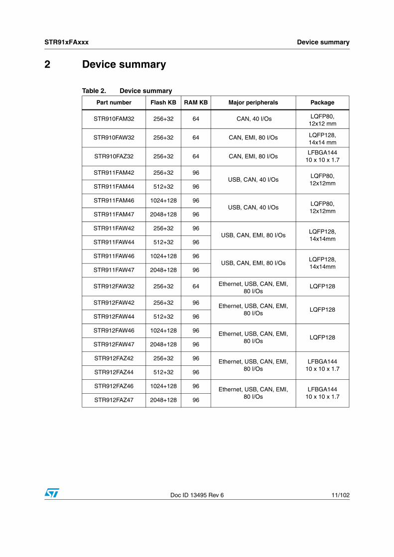
2 Device summary
Table 2. Device summary
Part number Flash KB RAM KB Major peripherals Package
STR910FAM32 256+32 64 CAN, 40 I/Os LQFP80, 12x12 mm
STR910FAW32 256+32 64 CAN, EMI, 80 I/Os LQFP128, 14x14 mm
STR910FAZ32 256+32 64 CAN, EMI, 80 I/OsLFBGA144
10 x 10 x 1.7
STR911FAM42 256+32 96USB, CAN, 40 I/Os
LQFP80, 12x12mmSTR911FAM44 512+32 96
STR911FAM46 1024+128 96USB, CAN, 40 I/Os
LQFP80, 12x12mmSTR911FAM47 2048+128 96
STR911FAW42 256+32 96USB, CAN, EMI, 80 I/Os
LQFP128, 14x14mmSTR911FAW44 512+32 96
STR911FAW46 1024+128 96USB, CAN, EMI, 80 I/Os
LQFP128, 14x14mmSTR911FAW47 2048+128 96
STR912FAW32 256+32 64 Ethernet, USB, CAN, EMI, 80 I/Os
LQFP128
STR912FAW42 256+32 96 Ethernet, USB, CAN, EMI, 80 I/Os
LQFP128STR912FAW44 512+32 96
STR912FAW46 1024+128 96 Ethernet, USB, CAN, EMI, 80 I/Os
LQFP128STR912FAW47 2048+128 96
STR912FAZ42 256+32 96 Ethernet, USB, CAN, EMI, 80 I/Os
LFBGA14410 x 10 x 1.7STR912FAZ44 512+32 96
STR912FAZ46 1024+128 96 Ethernet, USB, CAN, EMI, 80 I/Os
LFBGA14410 x 10 x 1.7STR912FAZ47 2048+128 96
Functional overview STR91xFAxxx
12/102 Doc ID 13495 Rev 6
3 Functional overview
3.1 System-in-a-package (SiP)The STR91xFA is a SiP device, comprised of two stacked die. One die is the ARM966E-S CPU with peripheral interfaces and analog functions, and the other die is the burst Flash. The two die are connected to each other by a custom high-speed 32-bit burst memory interface and a serial JTAG test/programming interface.
3.2 Package choiceSTR91xFA devices are available in 128-pin (14 x 14 mm) and 80-pin (12 x 12 mm) LQFP and LFBGA144 (10 x 10 mm) packages. Refer to Table 2: Device summary on page 11 for a list of available peripherals for each of the package choices.
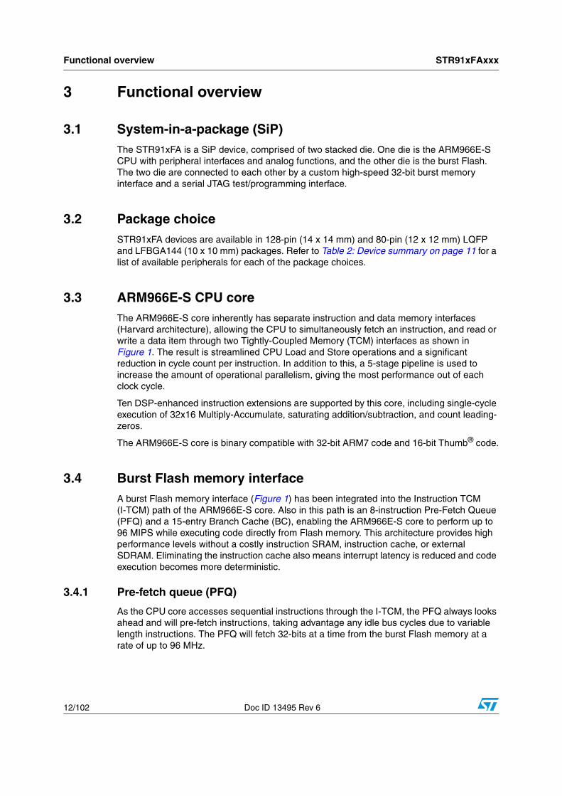
3.3 ARM966E-S CPU coreThe ARM966E-S core inherently has separate instruction and data memory interfaces (Harvard architecture), allowing the CPU to simultaneously fetch an instruction, and read or write a data item through two Tightly-Coupled Memory (TCM) interfaces as shown in Figure 1. The result is streamlined CPU Load and Store operations and a significant reduction in cycle count per instruction. In addition to this, a 5-stage pipeline is used to increase the amount of operational parallelism, giving the most performance out of each clock cycle.
Ten DSP-enhanced instruction extensions are supported by this core, including single-cycle execution of 32x16 Multiply-Accumulate, saturating addition/subtraction, and count leading-zeros.
The ARM966E-S core is binary compatible with 32-bit ARM7 code and 16-bit Thumb® code.
3.4 Burst Flash memory interfaceA burst Flash memory interface (Figure 1) has been integrated into the Instruction TCM (I-TCM) path of the ARM966E-S core. Also in this path is an 8-instruction Pre-Fetch Queue (PFQ) and a 15-entry Branch Cache (BC), enabling the ARM966E-S core to perform up to 96 MIPS while executing code directly from Flash memory. This architecture provides high performance levels without a costly instruction SRAM, instruction cache, or external SDRAM. Eliminating the instruction cache also means interrupt latency is reduced and code execution becomes more deterministic.
3.4.1 Pre-fetch queue (PFQ)
As the CPU core accesses sequential instructions through the I-TCM, the PFQ always looks ahead and will pre-fetch instructions, taking advantage any idle bus cycles due to variable length instructions. The PFQ will fetch 32-bits at a time from the burst Flash memory at a rate of up to 96 MHz.

STR91xFAxxx Functional overview
Doc ID 13495 Rev 6 13/102
3.4.2 Branch cache (BC)
When instruction addresses are not sequential, such as a program branch situation, the PFQ would have to flush and reload which would cause the CPU to stall if no BC were present. Before reloading, the PFQ checks the BC to see if it contains the desired target branch address. The BC contains up to fifteen of the most recently taken branch addresses and the first eight instructions associated with each of these branches. This check is extremely fast, checking all fifteen BC entries simultaneously for a branch address match (cache hit). If there is a hit, the BC rapidly supplies the instruction and reduces the CPU stall. This gives the PFQ time to start pre-fetching again while the CPU consumes these eight instructions from the BC. The advantage here is that program loops (very common with embedded control applications) run very fast if the address of the loops are contained in the BC.
In addition, there is a 16th branch cache entry that is dedicated to the Vectored Interrupt Controller (VIC) to further reduce interrupt latency by eliminating the stall latency typically imposed by fetching the instruction that reads the interrupt vector address from the VIC.
3.4.3 Management of literals
Typical ARM architecture and compilers do not place literals (data constants) sequentially in Flash memory with the instructions that use them, but instead the literals are placed at some other address which looks like a program branch from the PFQ’s point of view. The STR91xFA implementation of the ARM966E-S core has special circuitry to prevent flushing the PFQ when literals are encountered in program flow to keep performance at a maximum.

Functional overview STR91xFAxxx
14/102 Doc ID 13495 Rev 6
Figure 1. STR91xFA block diagram
STR91x
External MemoryInterface (EMI)***,
Muxed Address/Data
USB* Full Speed, 10Endpoints with FIFOs
Programmable DMAController (8 ch.)
AHBto
APB
PLL, Power Management,and Supervisory Reset
AH
B
APB
4 MHz to 25MHz XTAL
USB Bus
JTAG
VDD
VDDQ
GND
CORE SUPPLY, VDD
I/O SUPPLY, VDDQ
(4) 16-bit Timers,CAPCOM, PWM
8 Channel 10-bitADC
CAN 2.0B
(2) SPI
(2) I2C
Motor Control,3-ph Induction
(80) GPIO****
(3) UART w/ IrDA
Requestfrom
UART,I2C,SPI,
Timers,Ext Req
* USB not available on STR910
Programmable VectoredInterrupt Controller
Ethernet**MAC, 10/100
DedicatedDMA
To EthernetPHY (MII) **
EMI Ctrl
AMBA / AHBAInterface
Control Logic / BIU and Write Buffer
Data TCMInterface
ARM966E-SRISC CPU Core
InstructionTCM
InterfaceJTAGDebug
andETM
64K or 96KByte
SRAM
Arbiter
Burst Interface
Pre-Fetch Queand Branch
Cache
Stacked Burst Flash Memory Die
Main Flash 256K,512K, 1M or 2M
Bytes
Burst Interface
2nd Flash32K or 128K
Bytes
JTAG ISP
CORE GND, VSS
Real Time Clock 32.768 kHzXTAL
Wake Up
Watchdog Tmr
Ethe
rnet
**or
16
GPI
O
ETM
Programmable VectoredInterrupt Controllers
16
MU
X to
48
GPI
O
32 48
GND I/O GND, VSSQ
AVDD
AVREF*
AVSS
BACKUPSUPPLY
VBATT
RTC
*** EMI not available on LQFP80** Ethernet MAC not available on STR910 and STR911
EMI b
us**
* or
16 G
PIO
**** Only 40 GPIOs on LQFP80
ADC
STR91xA
STR91xFAxxx Functional overview
Doc ID 13495 Rev 6 15/102
3.5 SRAM (64 Kbytes or 96 Kbytes)A 32-bit wide SRAM resides on the CPU’s Data TCM (D-TCM) interface, providing single-cycle data accesses. As shown in Figure 1, the D-TCM shares SRAM access with the Advanced High-performance Bus (AHB). Sharing is controlled by simple arbitration logic to allow the DMA unit on the AHB to also access the SRAM.
3.5.1 Arbitration
Zero-wait state access occurs for either the D-TCM or the AHB when only one of the two is requesting SRAM. When both request SRAM simultaneously, access is granted on an interleaved basis so neither requestor is starved, granting one 32-bit word transfer to each requestor before relinquishing SRAM to the other. When neither the D-TCM or the AHB are requesting SRAM, the arbiter leaves access granted to the most recent user (if D-TCM was last to use SRAM then the D-TCM will not have to arbitrate to get access next time).
The CPU may execute code from SRAM through the AHB. There are no wait states as long as the D-TCM is not contending for SRAM access and the AHB is not sharing bandwidth with peripheral traffic. The ARM966E-S CPU core has a small pre-fetch queue built into this instruction path through the AHB to look ahead and fetch instructions during idle bus cycles.
3.5.2 Battery backup
When a battery is connected to the designated battery backup pin (VBATT), SRAM contents are automatically preserved when the operating voltage on the main digital supplies (VDD and VDDQ are lost or sag below the LVD threshold. Automatic switchover to SRAM can be disabled by firmware if it is desired that the battery will power only the RTC and not the SRAM during standby.
3.6 DMA data movementDMA channels on the Advanced High-performance Bus (AHB) take full advantage of the separate data path provided by the Harvard architecture, moving data rapidly and largely independent of the instruction path. There are two DMA units, one is dedicated to move data between the Ethernet interface and SRAM, the other DMA unit has eight programmable channels with 14 request signals to service other peripherals and interfaces (USB, SSP, ADC, UART, Timers, EMI, and external request pins). Both single word and burst DMA transfers are supported. Memory-to-memory transfers are supported in addition to memory-peripheral transfers. DMA access to SRAM is shared with D-TCM accesses, and arbitration is described in Section 3.5.1. Efficient DMA transfers are managed by firmware using linked list descriptor tables. Of the 16 DMA request signals, two are assigned to external inputs. The DMA unit can move data between external devices and resources inside the STR91xFA through the EMI bus.
Functional overview STR91xFAxxx
16/102 Doc ID 13495 Rev 6
3.7 Non-volatile memoriesThere are two independent 32-bit wide burst Flash memories enabling true read-while-write operation. The Flash memories are single-voltage erase/program with 20 year minimum data retention and 100K minimum erase cycles. The primary Flash memory is much larger than the secondary Flash.
Both Flash memories are blank when devices are shipped from ST. The CPU can boot only from Flash memory (configurable selection of which Flash bank).
Flash memories are programmed half-word (16 bits) at a time, but are erased by sector or by full array.
3.7.1 Primary Flash memory
Using the STR91xFA device configuration software tool and 3rd party Integrated Developer Environments, it is possible to specify that the primary Flash memory is the default memory from which the CPU boots at reset, or otherwise specify that the secondary Flash memory is the default boot memory. This choice of boot memory is non-volatile and stored in a location that can be programmed and changed only by JTAG In-System Programming. See Section 6: Memory mapping, for more detail.
The primary Flash memory has equal length 64K byte sectors. See Table 3 for number of sectors per device type.
3.7.2 Secondary Flash memory
The smaller of the two Flash memories can be used to implement a bootloader, capable of storing code to perform robust In-Application Programming (IAP) of the primary Flash memory. The CPU executes code from the secondary Flash, while updating code in the primary Flash memory. New code for the primary Flash memory can be downloaded over any of the interfaces on the STR91xFA (USB, Ethernet, CAN, UART, etc.)
Additionally, the secondary Flash memory may also be used to store small data sets by emulating EEPROM through firmware, eliminating the need for external EEPROM memories. This raises the data security level because passcodes and other sensitive information can be securely locked inside the STR91xFA device.
The secondary Flash memory is sectored as shown in Table 4 according to device type.
Both the primary Flash memory and the secondary Flash memory can be programmed with code and/or data using the JTAG In-System Programming (ISP) channel, totally independent of the CPU. This is excellent for iterative code development and for manufacturing.
Table 3. Sectoring of primary Flash memory
Size of primary Flash 256 Kbytes 512 Kbytes 1 Mbyte 2 Mbytes
Number of sectors 4 8 16 32
Size of each sector 64 Kbytes 64 Kbytes
STR91xFAxxx Functional overview
Doc ID 13495 Rev 6 17/102
3.8 One-time-programmable (OTP) memoryThere are 32 bytes of OTP memory ideally suited for serial numbers, security keys, factory calibration constants, or other permanent data constants. These OTP data bytes can be programmed only one time through either the JTAG interface or by the CPU, and these bytes can never be altered afterwards. As an option, a “lock bit” can be set by the JTAG interface or the CPU which will block any further writing to the this OTP area. The “lock bit” itself is also OTP. If the OTP array is unlocked, it is always possible to go back and write to an OTP byte location that has not been previously written, but it is never possible to change an OTP byte location if any one bit of that particular byte has been written before. The last two OTP bytes (bytes 31 and 30) are reserved for the STR91xFA product ID and revision level.
3.8.1 Product ID and revision level
OTP bytes 31 and 30 are programmed at ST factory before shipment and may be read by firmware to determine the STR91xFA product type and silicon revision so it can optionally take action based on the silicon on which it is running. In Rev H devices and 1MB/2MB Rev A devices, byte 31 contains the major family identifier of "9" (for STR9) in the high-nibble location and the minor family identifier in the low nibble location, which can be used to determine the size of primary flash memory. In all devices, byte 30 contains the silicon revision level indicator. See Table 5 for values related to the revisions of STR9 production devices and size of primary Flash memory. See Section 8 for details of external identification of silicon revisions.
Table 4. Sectoring of secondary Flash memory
Size of secondary Flash 32 Kbytes 128 Kbytes
Number of sectors 4 8
Size of each sector 8 Kbytes 16 Kbytes
Table 5. Product ID and revision level values
Production salestype Silicon revision Size of primary Flash OTP byte 31 OTP byte 30
STR91xFAxxxxx Rev G 256K or 512K 91h 20h
STR91xFAxxxxx Rev H 256K 90h 21h
STR91xFAxxxxx Rev H 512K 91h 21h
STR91xFAx46xx Rev A 1024K 92h 21h
STR91xFAx47xx Rev A 2048K 93h 21h

Functional overview STR91xFAxxx
18/102 Doc ID 13495 Rev 6
3.9 Vectored interrupt controller (VIC)Interrupt management in the STR91xFA is implemented from daisy-chaining two standard ARM VIC units. This combined VIC has 32 prioritized interrupt request channels and generates two interrupt output signals to the CPU. The output signals are FIQ and IRQ, with FIQ having higher priority.
3.9.1 FIQ handling
FIQ (Fast Interrupt reQuest) is the only non-vectored interrupt and the CPU can execute an Interrupt Service Routine (ISR) directly without having to determine/prioritize the interrupt source, minimizing ISR latency. Typically only one interrupt source is assigned to FIQ. An FIQ interrupt has its own set of banked registers to minimize the time to make a context switch. Any of the 32 interrupt request input signals coming into the VIC can be assigned to FIQ.
3.9.2 IRQ handling
IRQ is a vectored interrupt and is the logical OR of all 32 interrupt request signals coming into the 32 IRQ channels. Priority of individual vectored interrupt requests is determined by hardware (IRQ channel Intr 0 is highest priority, IRQ channel Intr 31 is lowest).
However, inside the same VIC (primary or secondary VIC), CPU firmware may re-assign individual interrupt sources to individual hardware IRQ channels, meaning that firmware can effectively change interrupt priority levels as needed within the same VIC (from priority 0 to priority 16).
Note: VIC0 (primary VIC) interrupts always have higher priority than VIC1 (secondary VIC) interrupts
When the IRQ signal is activated by an interrupt request, VIC hardware will resolve the IRQ interrupt priority, then the ISR reads the VIC to determine both the interrupt source and the vector address to jump to the service code.
The STR91xFA has a feature to reduce ISR response time for IRQ interrupts. Typically, it requires two memory accesses to read the interrupt vector address from the VIC, but the STR91xFA reduces this to a single access by adding a 16th entry in the instruction branch cache, dedicated for interrupts. This 16th cache entry always holds the instruction that reads the interrupt vector address from the VIC, eliminating one of the memory accesses typically required in traditional ARM implementations.
3.9.3 Interrupt sources
The 32 interrupt request signals coming into the VIC on 32 IRQ channels are from various sources; 5 from a wake-up unit and the remaining 27 come from internal sources on the STR91xFA such as on-chip peripherals, see Table 6. Optionally, firmware may force an interrupt on any IRQ channel.
One of the 5 interrupt requests generated by the wake-up unit (IRQ25 in Table 6) is derived from the logical OR of all 32 inputs to the wake-up unit. Any of these 32 inputs may be used to wake up the CPU and cause an interrupt. These 32 inputs consist of 30 external interrupts on selected and enabled GPIO pins, plus the RTC interrupt, and the USB Resume interrupt.

STR91xFAxxx Functional overview
Doc ID 13495 Rev 6 19/102
Each of 4 remaining interrupt requests generated by the wake-up unit (IRQ26 in Table 6) are derived from groupings of 8 interrupt sources. One group is from GPIO pins P3.2 to P3.7 plus the RTC interrupt and the USB Resume interrupt; the next group is from pins P5.0 to P5.7; the next group is from pins P6.0 to P6.7; and last the group is from pins P7.0 to P7.7. This allows individual pins to be assigned directly to vectored IRQ interrupts or one pin assigned directly to the non-vectored FIQ interrupt.
Table 6. VIC IRQ channels
IRQ channel hardware priority
VIC input channel
Logic block Interrupt source
0 (high priority) VIC0.0 Watchdog Timeout in WDT mode, Terminal Count in Counter Mode
1 VIC0.1 CPU Firmware Firmware generated interrupt
2 VIC0.2 CPU Core Debug Receive Command
3 VIC0.3 CPU Core Debug Transmit Command
4 VIC0.4 TIM Timer 0 Logic OR of ICI0_0, ICI0_1, OCI0_0, OCI0_1, Timer overflow
5 VIC0.5 TIM Timer 1 Logic OR of ICI1_0, ICI1_1, OCI1_0, OCI1_1, Timer overflow
6 VIC0.6 TIM Timer 2 Logic OR of ICI2_0, ICI2_1, OCI2_0, OCI2_1, Timer overflow
7 VIC0.7 TIM Timer 3 Logic OR of ICI3_0, ICI3_1, OCI3_0, OCI3_1, Timer overflow
8 VIC0.8 USB Logic OR of high priority USB interrupts
9 VIC0.9 USB Logic OR of low priority USB interrupts
10 VIC0.10 CCU Logic OR of all interrupts from Clock Control Unit
11 VIC0.11 Ethernet MACLogic OR of Ethernet MAC interrupts via its own dedicated DMA
channel.
12 VIC0.12 DMALogic OR of interrupts from each of the 8 individual DMA
channels
13 VIC0.13 CAN Logic OR of all CAN interface interrupt sources
14 VIC0.14 IMC Logic OR of 8 Induction Motor Control Unit interrupts
15 VIC0.15 ADC End of AtoD conversion interrupt
16 VIC1.0 UART0 Logic OR of 5 interrupts from UART channel 0
17 VIC1.1 UART1 Logic OR of 5 interrupts from UART channel 1
18 VIC1.2 UART2 Logic OR of 5 interrupts from UART channel 2
19 VIC1.3 I2C0Logic OR of transmit, receive, and error interrupts of I2C channel
0
20 VIC1.4 I2C1Logic OR of transmit, receive, and error interrupts of I2C channel
1
21 VIC1.5 SSP0 Logic OR of all interrupts from SSP channel 0
22 VIC1.6 SSP1 Logic OR of all interrupts from SSP channel 1
23 VIC1.7 BROWNOUT LVD warning interrupt
24 VIC1.8 RTC Logic OR of Alarm, Tamper, or Periodic Timer interrupts

Functional overview STR91xFAxxx
20/102 Doc ID 13495 Rev 6
3.10 Clock control unit (CCU)The CCU generates a master clock of frequency fMSTR. From this master clock the CCU also generates individually scaled and gated clock sources to each of the following functional blocks within the STR91xFA.
CPU, fCPUCLK
Advanced High-performance Bus (AHB), fHCLK
Advanced Peripheral Bus (APB), fPCLK
Flash Memory Interface (FMI), fFMICLK
External Memory Interface (EMI), fBCLK
UART Baud Rate Generators, fBAUD
USB, fUSB
3.10.1 Master clock sources
The master clock in the CCU (fMSTR) is derived from one of three clock input sources. Under firmware control, the CPU can switch between the three CCU inputs without introducing any glitches on the master clock output. Inputs to the CCU are:
Main Oscillator (fOSC). The source for the main oscillator input is a 4 to 25 MHz external crystal connected to STR91xFA pins X1_CPU and X2_CPU, or an external oscillator device connected to pin X1_CPU.
PLL (fPLL). The PLL takes the 4 to 25 MHz oscillator clock as input and generates a master clock output up to 96 MHz (programmable). By default, at power-up the master clock is sourced from the main oscillator until the PLL is ready (locked) and then the CPU may switch to the PLL source under firmware control. The CPU can switch back to the main oscillator source at any time and turn off the PLL for low-power operation. The PLL is always turned off in Sleep mode.
RTC (fRTC). A 32.768 kHz external crystal can be connected to pins X1_RTC and X2_RTC, or an external oscillator connected to pin X1_RTC to constantly run the real-time clock unit. This 32.768 kHz clock source can also be used as an input to the CCU to run the CPU in slow clock mode for reduced power.
25 VIC1.9 Wake-Up (all)Logic OR of all 32 inputs of Wake-Up unit (30 pins, RTC, and
USB Resume)
26 VIC1.10 Wake-up Group 0Logic OR of 8 interrupt sources: RTC, USB Resume, pins P3.2 to
P3.7
27 VIC1.11 Wake-up Group 1 Logic OR of 8 interrupts from pins P5.0 to P5.7
28 VIC1.12 Wake-up Group 2 Logic OR of 8 interrupts from pins P6.0 to P6.7
29 VIC1.13 Wake-up Group 3 Logic OR of 8 interrupts from pins P7.0 to P7.7
30 VIC1.14 USB USB Bus Resume Wake-up (also input to wake-up unit)
31 (low priority) VIC1.15 PFQ-BC Special use of interrupts from Prefetch Queue and Branch Cache
Table 6. VIC IRQ channels (continued)
IRQ channel hardware priority
VIC input channel
Logic block Interrupt source
STR91xFAxxx Functional overview
Doc ID 13495 Rev 6 21/102
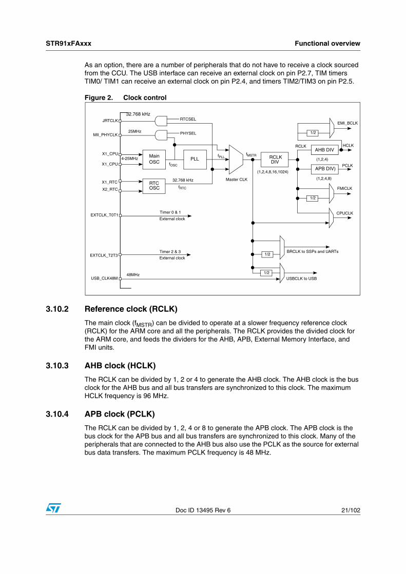
As an option, there are a number of peripherals that do not have to receive a clock sourced from the CCU. The USB interface can receive an external clock on pin P2.7, TIM timers TIM0/ TIM1 can receive an external clock on pin P2.4, and timers TIM2/TIM3 on pin P2.5.
Figure 2. Clock control
3.10.2 Reference clock (RCLK)
The main clock (fMSTR) can be divided to operate at a slower frequency reference clock (RCLK) for the ARM core and all the peripherals. The RCLK provides the divided clock for the ARM core, and feeds the dividers for the AHB, APB, External Memory Interface, and FMI units.
3.10.3 AHB clock (HCLK)
The RCLK can be divided by 1, 2 or 4 to generate the AHB clock. The AHB clock is the bus clock for the AHB bus and all bus transfers are synchronized to this clock. The maximum HCLK frequency is 96 MHz.
3.10.4 APB clock (PCLK)
The RCLK can be divided by 1, 2, 4 or 8 to generate the APB clock. The APB clock is the bus clock for the APB bus and all bus transfers are synchronized to this clock. Many of the peripherals that are connected to the AHB bus also use the PCLK as the source for external bus data transfers. The maximum PCLK frequency is 48 MHz.
MII_PHYCLK25MHz PHYSEL
X1_CPU
X1_CPU
X1_RTC
X2_RTC
EXTCLK_T0T1
EXTCLK_T2T3
USB_CLK48M
4-25MHz
48MHz
MainOSC
RTCOSC
fOSC
PLL
32.768 kHz
fRTC
Timer 0 & 1
fPLLfMSTR
Master CLK
1/2
1/2
RCLKDIV
(1,2,4,8,16,1024)
USBCLK to USB
RCLKAHB DIV
(1,2,4)
APB DIV)
(1,2,4,8)
1/2
HCLK
PCLK
FMICLK
CPUCLK
Timer 2 & 3
1/2
EMI_BCLKJRTCLK RTCSEL
32.768 kHz
External clock
External clock
BRCLK to SSPs and UARTs
Functional overview STR91xFAxxx
22/102 Doc ID 13495 Rev 6
3.10.5 Flash memory interface clock (FMICLK)
The FMICLK clock is an internal clock derived from RCLK, defaulting to RCLK frequency at power up. The clock can be optionally divided by 2. The FMICLK determines the bus bandwidth between the ARM core and the Flash memory. Typically, codes in the Flash memory can be fetched one word per FMICLK clock in burst mode. The maximum FMICLK frequency is 96 MHz.
3.10.6 UART and SSP clock (BRCLK)
BRCLK is an internal clock derived from fMSTR that is used to drive the two SSP peripherals and to generate the Baud rate for the three on-chip UART peripherals. The frequency can be optionally divided by 2.
3.10.7 External memory interface bus clock (BCLK)
The BCLK is an internal clock that controls the EMI bus. All EMI bus signals are synchronized to the BCLK. The BCLK is derived from the HCLK and the frequency can be configured to be the same or half that of the HCLK. Refer to Table 17 on page 66 for the maximum BCLK frequency (fBCLK). The BCLK clock is available on the LFBGA package as an output pin.
3.10.8 USB interface clock
Special consideration regarding the USB interface: The clock to the USB interface must operate at 48 MHz and comes from one of three sources, selected under firmware control:
CCU master clock output of 48 MHz.
CCU master clock output of 96 MHz. An optional divided-by-two circuit is available to produce 48 MHz for the USB while the CPU system runs at 96MHz.
STR91xFA pin P2.7. An external 48 MHz oscillator connected to pin P2.7 can directly source the USB while the CCU master clock can run at some frequency other than 48 or 96 MHz.
3.10.9 Ethernet MAC clock
Special consideration regarding the Ethernet MAC: The external Ethernet PHY interface device requires it’s own 25 MHz clock source. This clock can come from one of two sources:
A 25 MHz clock signal coming from a dedicated output pin (P5.2) of the STR91xFA. In this case, the STR91xFA must use a 25 MHz signal on its main oscillator input in order to pass this 25 MHz clock back out to the PHY device through pin P5.2. The advantage here is that an inexpensive 25 MHz crystal may be used to source a clock to both the STR91xFA and the external PHY device.
An external 25 MHz oscillator connected directly to the external PHY interface device. In this case, the STR91xFA can operate independent of 25 MHz.
3.10.10 External RTC calibration clock
The RTC_CLK can be enabled as an output on the JRTCK pin. The RTC_CLK is used for RTC oscillator calibration. The RTC_CLK is active in Sleep mode and can be used as a system wake up control clock.
STR91xFAxxx Functional overview
Doc ID 13495 Rev 6 23/102
3.10.11 Operation example
As an example of CCU operation, a 25 MHz crystal can be connected to the main oscillator input on pins X1_CPU and X2_CPU, a 32.768 kHz crystal connected to pins X1_RTC and X2_RTC, and the clock input of an external Ethernet PHY device is connected to STR91xFA output pin P5.2. In this case, the CCU can run the CPU at 96 MHz from PLL, the USB interface at 48 MHz, and the Ethernet interface at 25 MHz. The RTC is always running in the background at 32.768 kHz, and the CPU can go to very low power mode dynamically by running from 32.768 kHz and shutting off peripheral clocks and the PLL as needed.
3.11 Flexible power managementThe STR91xFA offers configurable and flexible power management control that allows the user to choose the best power option to fit the application. Power consumption can be dynamically managed by firmware and hardware to match the system’s requirements. Power management is provided via clock control to the CPU and individual peripherals.
Clocks to the CPU and peripherals can be individually divided and gated off as needed. In addition to individual clock divisors, the CCU master clock source going to the CPU, AHB, APB, EMI, and FMI can be divided dynamically by as much as 1024 for low power operation. Additionally, the CCU may switch its input to the 32.768 kHz RTC clock at any time for low power.
The STR91xFA supports the following three global power control modes:
Run Mode: All clocks are on with option to gate individual clocks off via clock mask registers.
Idle Mode: CPU and FMI clocks are off until an interrupt, reset, or wake-up occurs. Pre-configured clock mask registers selectively allow individual peripheral clocks to continue run during Idle Mode.
Sleep Mode: All clocks off except RTC clock. Wake up unit remains powered, PLL is forced off.
A special mode is used when JTAG debug is active which never gates off any clocks even if the CPU enters Idle or Sleep mode.
3.11.1 Run mode
This is the default mode after any reset occurs. Firmware can gate off or scale any individual clock. Also available is a special Interrupt Mode which allows the CPU to automatically run full speed during an interrupt service and return back to the selected CPU clock divisor rate when the interrupt has been serviced. The advantage here is that the CPU can run at a very low frequency to conserve power until a periodic wake-up event or an asynchronous interrupt occurs at which time the CPU runs full speed immediately.

Functional overview STR91xFAxxx
24/102 Doc ID 13495 Rev 6
3.11.2 Idle mode
In this mode the CPU suspends code execution and the CPU and FMI clocks are turned off immediately after firmware sets the Idle Bit. Various peripherals continue to run based on the settings of the mask registers that exist just prior to entering Idle Mode. There are 3 ways to exit Idle Mode and return to Run Mode:
Any reset (external reset pin, watchdog, low-voltage, power-up, JTAG debug command)
Any interrupt (external, internal peripheral, RTC alarm or interval)
Input from wake-up unit on GPIO pins
Note: It is possible to remain in Idle Mode for the majority of the time and the RTC can be programmed to periodically wake up to perform a brief task or check status.
3.11.3 Sleep mode
In this mode all clock circuits except the RTC are turned off and main oscillator input pins X1_CPU and X2_CPU are disabled. The RTC clock is required for the CPU to exit Sleep Mode. The entire chip is quiescent (except for RTC and wake-up circuitry). There are three means to exit Sleep Mode and re-start the system:
Some resets (external reset pin, low-voltage, power-up, JTAG debug command)
RTC alarm
Input from wake-up unit
3.12 Voltage suppliesThe STR91xFA requires two separate operating voltage supplies. The CPU and memories operate from a 1.65V to 2.0V on the VDD pins, and the I/O ring operates at 2.7V to 3.6V on the VDDQ pins.
In Standby mode, both VDD and VDDQ must be shut down. Otherwise the specified maximum power consumption for Standby mode (IRTC_STBY and ISRAM_STBY) may be exceeded. Leakage may occur if only one of the voltage supplies is off.
3.12.1 Independent A/D converter supply and reference voltage
The ADC unit on 128-pin and 144-ball packages has an isolated analog voltage supply input at pin AVDD to accept a very clean voltage source, independent of the digital voltage supplies. Additionally, an isolated analog supply ground connection is provided on pin AVSS only on 128-pin and 144-ball packages for further ADC supply isolation. On 80-pin packages, the analog voltage supply is shared with the ADC reference voltage pin (as described next), and the analog ground is shared with the digital ground at a single point in the STR91xFA device on pin AVSS_VSSQ.
A separate external analog reference voltage input for the ADC unit is available on 128-pin and 144-ball packages at the AVREF pin for better accuracy on low voltage inputs. For 80-pin packages, the ADC reference voltage is tied internally to the ADC unit supply voltage at pin AVREF_AVDD, meaning the ADC reference voltage is fixed to the ADC unit supply voltage.
See Table 11: Operating conditions, for restrictions to the relative voltage levels of VDDQ, AVDD, AVREF, and AVREF_AVDD.

STR91xFAxxx Functional overview
Doc ID 13495 Rev 6 25/102
3.12.2 Battery supply
An optional stand-by voltage from a battery or other source may be connected to pin VBATT to retain the contents of SRAM in the event of a loss of the main digital supplies (VDD and VDDQ) . The SRAM will automatically switch its supply from the internal VDD source to the VBATT pin when the voltage of VDD drops below the LVD threshold. In order to use the battery supply, the LVD must be enabled.
The VBATT pin also supplies power to the RTC unit, allowing the RTC to function even when the main digital supplies (VDD and VDDQ) are switched off. By configuring the RTC register, it is possible to select whether or not to power from VBATT only the RTC unit, or power the RTC unit and the SRAM when the STR91xFA device is powered off.
3.13 System supervisorThe STR91xFA monitors several system and environmental inputs and will generate a global reset, a system reset, or an interrupt based on the nature of the input and configurable settings. A global reset clears all functions on the STR91xFA, a system reset will clear all but the Clock Control Unit (CCU) settings and the system status register. At any time, firmware may reset individual on-chip peripherals. System supervisor inputs include:
GR: CPU voltage supply (VDD) drop out or brown out
GR: I/O voltage supply (VDDQ) drop out or brown out
GR: Power-Up condition
SR: Watchdog timer timeout
SR: External reset pin (RESET_INn)
SR: JTAG debug reset command
Note: GR: means the input causes Global Reset, SR: means the input causes System Reset
The CPU may read a status register after a reset event to determine if the reset was caused by a watchdog timer timeout or a voltage supply drop out. This status register is cleared only by a power up reset.
3.13.1 Supply voltage brownout
Each operating voltage source (VDD and VDDQ) is monitored separately by the Low Voltage Detect (LVD) circuitry. The LVD will generate an early warning interrupt to the CPU when voltage sags on either VDD or VDDQ voltage inputs. This is an advantage for battery powered applications because the system can perform an orderly shutdown before the batteries become too weak. The voltage trip point to cause a brown out interrupt is typically 0.25V above the LVD dropout thresholds that cause a reset.
CPU firmware may prevent all brown-out interrupts by writing to interrupt mask registers at run-time.

Functional overview STR91xFAxxx
26/102 Doc ID 13495 Rev 6
3.13.2 Supply voltage dropout
LVD circuitry will always cause a global reset if the CPU’s VDD source drops below it’s fixed threshold of 1.4 V.
However, the LVD trigger threshold to cause a global reset for the I/O ring’s VDDQ source is set to one of two different levels, depending if VDDQ will be operated in the range of 2.7 V to 3.3 V, or 3.0V to 3.6 V. If VDDQ operation is at 2.7 V to 3.3 V, the LVD dropout trigger threshold is 2.4 V. If VDDQ operation is 3.0 V and 3.6 V, the LVD threshold is 2.7 V. The choice of trigger level is made by STR91xFA device configuration software from STMicroelectronics or IDE from 3rd parties, and is programmed into the STR91xFA device along with other configurable items through the JTAG interface when the Flash memory is programmed.
CPU firmware may prevent some LVD resets if desired by writing a control register at run-time. Firmware may also disable the LVD completely for lowest-power operation when an external LVD device is being used.
3.13.3 Watchdog timer
The STR91xFA has a 16-bit down-counter (not one of the four TIM timers) that can be used as a watchdog timer or as a general purpose free-running timer/counter. The clock source is the peripheral clock from the APB, and an 8-bit clock pre-scaler is available. When enabled by firmware as a watchdog, this timer will cause a system reset if firmware fails to periodically reload this timer before the terminal count of 0x0000 occurs, ensuring firmware sanity. The watchdog function is off by default after a reset and must be enabled by firmware.
3.13.4 External RESET_INn pin
This input signal is active-low with hystereses (VHYS). Other open-drain, active-low system reset signals on the circuit board (such as closure to ground from a push-button) may be connected directly to the RESET_INn pin, but an external pull-up resistor to VDDQ must be present as there is no internal pullup on the RESET_INn pin.
A valid active-low input signal of tRINMIN duration on the RESET_INn pin will cause a system reset within the STR91xFA. There is also a RESET_OUTn pin on the STR91xFA that can drive other system components on the circuit board. RESET_OUTn is active-low and has the same timing of the Power-On-Reset (POR) shown next, tPOR.
3.13.5 Power-up
The LVD circuitry will always generate a global reset when the STR91xFA powers up, meaning internal reset is active until VDDQ and VDD are both above the LVD thresholds. This POR condition has a duration of tPOR, after which the CPU will fetch its first instruction from address 0x0000.0000 in Flash memory. It is not possible for the CPU to boot from any other source other than Flash memory.
3.13.6 JTAG debug command
When the STR91xFA is in JTAG debug mode, an external device which controls the JTAG interface can command a system reset to the STR91xFA over the JTAG channel.

STR91xFAxxx Functional overview
Doc ID 13495 Rev 6 27/102
3.13.7 Tamper detection
On 128-pin and 144-ball STR91xFA devices only, there is a tamper detect input pin, TAMPER_IN, used to detect and record the time of a tamper event on the end product such as malicious opening of an enclosure, unwanted opening of a panel, etc. The activation mode of the tamper pin detects when a signal on the tamper input pin is driven from low-to-high, or high-to-low depending on firmware configuration. Once a tamper event occurs, the RTC time (millisecond resolution) and the date are recorded in the RTC unit. Simultaneously, the SRAM standby voltage source will be cut off to invalidate all SRAM contents. Tamper detection control and status logic are part of the RTC unit.
3.14 Real-time clock (RTC)The RTC combines the functions of a complete time-of-day clock (millisecond resolution) with an alarm programmable up to one month, a 9999-year calender with leap-year support, periodic interrupt generation from 1 to 512 Hz, tamper detection (described in Section 3.13.7), and an optional clock calibration output on the JRTCK pin. The time is in 24 hour mode, and time/calendar values are stored in binary-coded decimal format.
The RTC also provides a self-isolation mode that is automatically activated during power down. This feature allows the RTC to continue operation when VDDQ and VDD are absent, as long as an alternate power source, such as a battery, is connected to the VBATT input pin. The current drawn by the RTC unit on the VBATT pin is very low in this standby mode, IRTC_STBY.
3.15 JTAG interfaceAn IEEE-1149.1 JTAG interface on the STR91xFA provides In-System-Programming (ISP) of all memory, boundary scan testing of pins, and the capability to debug the CPU.
STR91xFA devices are shipped from ST with blank Flash memories. The CPU can only boot from Flash memory (selection of which Flash bank is programmable). Firmware must be initially programmed through JTAG into one of these Flash memories before the STR91xFA is used.
Six pins are used on this JTAG serial interface. The five signals JTDI, JTDO, JTMS, JTCK, and JTRSTn are all standard JTAG signals complying with the IEEE-1149.1 specification. The sixth signal, JRTCK (Return TCK), is an output from the STR91xFA and it is used to pace the JTCK clock signal coming in from the external JTAG test equipment for debugging. The frequency of the JTCK clock signal coming from the JTAG test equipment must be at least 10 times less than the ARM966E-S CPU core operating frequency (fCPUCLK). To ensure this, the signal JRTCK is output from the STR91xFA and is input to the external JTAG test equipment to hold off transitions of JTCK until the CPU core is ready, meaning that the JTAG equipment cannot send the next rising edge of JTCK until the equipment receives a rising edge of JRTCK from the STR91xFA. The JTAG test equipment must be able to interpret the signal JRTCK and perform this adaptive clocking function. If it is known that the CPU clock will always be at least ten times faster than the incoming JTCK clock signal, then the JRTCK signal is not needed.
The two die inside the STR91xFA (CPU die and Flash memory die) are internally daisy-chained on the JTAG bus, see Figure 3 on page 28. The CPU die has two JTAG Test Access Ports (TAPs), one for boundary scan functions and one for ARM CPU debug. The Flash memory die has one TAP for program/erase of non-volatile memory. Because these three
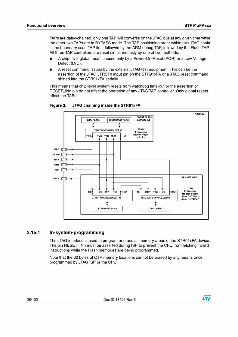
Functional overview STR91xFAxxx
28/102 Doc ID 13495 Rev 6
TAPs are daisy-chained, only one TAP will converse on the JTAG bus at any given time while the other two TAPs are in BYPASS mode. The TAP positioning order within this JTAG chain is the boundary scan TAP first, followed by the ARM debug TAP, followed by the Flash TAP. All three TAP controllers are reset simultaneously by one of two methods:
A chip-level global reset, caused only by a Power-On-Reset (POR) or a Low Voltage Detect (LVD).
A reset command issued by the external JTAG test equipment. This can be the assertion of the JTAG JTRSTn input pin on the STR91xFA or a JTAG reset command shifted into the STR91xFA serially.
This means that chip-level system resets from watchdog time-out or the assertion of RESET_INn pin do not affect the operation of any JTAG TAP controller. Only global resets effect the TAPs.
Figure 3. JTAG chaining inside the STR91xFA
3.15.1 In-system-programming
The JTAG interface is used to program or erase all memory areas of the STR91xFA device. The pin RESET_INn must be asserted during ISP to prevent the CPU from fetching invalid instructions while the Flash memories are being programmed.
Note that the 32 bytes of OTP memory locations cannot be erased by any means once programmed by JTAG ISP or the CPU.
JTDI
JTMS
JTCK
JTDO
TDI TMS TCK TDO
TDO TMS TCK TDI
JTAG TAP CONTROLLER #1
JTAG TAP CONTROLLER #3
BURST FLASHMEMORY DIE
ARM966ES DIE
BOUNDARY SCAN
STR91xx
JTRSTn
TRST TDI TMSTCK TDO
JTAG TAP CONTROLLER #2
CPU DEBUG
TRST
JRTCK
TRST
MAIN FLASH SECONDARY FLASH
JTAGInstruction
register length:5 bits for TAP #14 bits for TAP #2
JTAGInstruction
register lengthis 8 bits
STR91xFAxxx Functional overview
Doc ID 13495 Rev 6 29/102
3.15.2 Boundary scan
Standard JTAG boundary scan testing compliant with IEEE-1149.1 is available on the majority of pins of the STR91xFA for circuit board test during manufacture of the end product. STR91xFA pins that are not serviced by boundary scan are the following:
JTAG pins JTCK, JTMS, JTDI, JTDO, JTRSTn, JRTCK
Oscillator input pins X1_CPU, X2_CPU, X1_RTC, X2_RTC
Tamper detect input pin TAMPER_IN (128-pin and 144-pin packages only)
3.15.3 CPU debug
The ARM966E-S CPU core has standard ARM EmbeddedICE-RT logic, allowing the STR91xFA to be debugged through the JTAG interface. This provides advanced debugging features making it easier to develop application firmware, operating systems, and the hardware itself. Debugging requires that an external host computer, running debug software, is connected to the STR91xFA target system via hardware which converts the stream of debug data and commands from the host system’s protocol (USB, Ethernet, etc.) to the JTAG EmbeddedICE-RT protocol on the STR91xFA. These protocol converters are commercially available and operate with debugging software tools.
The CPU may be forced into a Debug State by a breakpoint (code fetch), a watchpoint (data access), or an external debug request over the JTAG channel, at which time the CPU core and memory system are effectively stopped and isolated from the rest of the system. This is known as Halt Mode and allows the internal state of the CPU core, memory, and peripherals to be examined and manipulated. Typical debug functions are supported such as run, halt, and single-step. The EmbeddedICE-RT logic supports two hardware compare units. Each can be configured to be either a watchpoint or a breakpoint. Breakpoints can also be data-dependent.
Debugging (with some limitations) may also occur through the JTAG interface while the CPU is running full speed, known as Monitor Mode. In this case, a breakpoint or watchpoint will not force a Debug State and halt the CPU, but instead will cause an exception which can be tracked by the external host computer running monitor software. Data can be sent and received over the JTAG channel without affecting normal instruction execution. Time critical code, such as Interrupt Service Routines may be debugged real-time using Monitor Mode.
3.15.4 JTAG security bit
This is a non-volatile bit (Flash memory based), which when set will not allow the JTAG debugger or JTAG programmer to read the Flash memory contents.
Using JTAG ISP, this bit is typically programmed during manufacture of the end product to prevent unwanted future access to firmware intellectual property. The JTAG Security Bit can be cleared only by a JTAG “Full Chip Erase” command, making the STR91xFA device blank (except for programmed OTP bytes), and ready for programming again. The CPU can read the status of the JTAG Security Bit, but it may not change the bit value.

Functional overview STR91xFAxxx
30/102 Doc ID 13495 Rev 6
3.16 Embedded trace module (ARM ETM9, v. r2p2)The ETM9 interface provides greater visibility of instruction and data flow happening inside the CPU core by streaming compressed data at a very high rate from the STR91xFA though a small number of ETM9 pins to an external Trace Port Analyzer (TPA) device. The TPA is connected to a host computer using USB, Ethernet, or other high-speed channel. Real-time instruction flow and data activity can be recorded and later formatted and displayed on the host computer running debugger software, and this software is typically integrated with the debug software used for EmbeddedICE-RT functions such as single-step, breakpoints, etc. Tracing may be triggered and filtered by many sources, such as instruction address comparators, data watchpoints, context ID comparators, and counters. State sequencing of up to three triggers is also provided. TPA hardware is commercially available and operates with debugging software tools.
The ETM9 interface is nine pins total, four of which are data lines, and all pins can be used for GPIO after tracing is no longer needed. The ETM9 interface is used in conjunction with the JTAG interface for trace configuration. When tracing begins, the ETM9 engine compresses the data by various means before broadcasting data at high speed to the TPA over the four data lines. The most common ETM9 compression technique is to only output address information when the CPU branches to a location that cannot be inferred from the source code. This means the host computer must have a static image of the code being executed for decompressing the ETM9 data. Because of this, self-modified code cannot be traced.
3.17 Ethernet MAC interface with DMASTR91xFA devices in 128-pin and 144-ball packages provide an IEEE-802.3-2002 compliant Media Access Controller (MAC) for Ethernet LAN communications through an industry standard Medium Independent Interface (MII). The STR91xFA requires an external Ethernet physical interface device (PHY) to connect to the physical LAN bus (twisted-pair, fiber, etc.). The PHY is connected to the STR91xFA MII port using as many as 18 signals (see pins which have signal names MII_* in Table 8).
The MAC corresponds to the OSI Data Link layer and the PHY corresponds to the OSI Physical layer. The STR91xFA MAC is responsible for:
Data encapsulation, including frame assembly before transmission, and frame parsing/error detection during and after reception.
Media access control, including initiation of frame transmission and recover from transmission failure.

STR91xFAxxx Functional overview
Doc ID 13495 Rev 6 31/102
The STR91xFA MAC includes the following features:
Supports 10 and 100 Mbps rates
Tagged MAC frame support (VLAN support)
Half duplex (CSMA/CD) and full duplex operation
MAC control sublayer (control frames) support
32-bit CRC generation and removal
Several address filtering modes for physical and multicast address (multicast and group addresses)
32-bit status code for each transmitted or received frame
Internal FIFOs to buffer transmit and receive frames. Transmit FIFO depth is 4 words (32 bits each), and the receive FIFO is 16 words deep.
A 32-bit burst DMA channel residing on the AHB is dedicated to the Ethernet MAC for high-speed data transfers, side-stepping the CPU for minimal CPU impact during transfers. This DMA channel includes the following features:
Direct SRAM to MAC transfers of transmit frames with the related status, by descriptor chain
Direct MAC to SRAM transfers of receive frames with the related status, by descriptor chain
Open and Closed descriptor chain management
3.18 USB 2.0 slave device interface with DMAThe STR91xFA provides a USB slave controller that implements both the OSI Physical and Data Link layers for direct bus connection by an external USB host on pins USBDP and USBPN. The USB interface detects token packets, handles data transmission and reception, and processes handshake packets as required by the USB 2.0 standard.
The USB slave interface includes the following features:
Supports USB low and full-speed transfers (12 Mbps), certified to comply with the USB 2.0 specification
Supports isochronous, bulk, control, and interrupt endpoints
Configurable number of endpoints allowing a mixture of up to 20 single-buffered monodirectional endpoints or up to 10 double-buffered bidirectional endpoints
Dedicated, dual-port 2 Kbyte USB Packet Buffer SRAM. One port of the SRAM is connected by a Packet Buffer Interface (PBI) on the USB side, and the CPU connects to the other SRAM port.
CRC generation and checking
NRZI encoding-decoding and bit stuffing
USB suspend resume operations

Functional overview STR91xFAxxx
32/102 Doc ID 13495 Rev 6
3.18.1 Packet buffer interface (PBI)
The PBI manages a set of buffers inside the 2 Kbyte Packet Buffer, both for transmission and reception. The PBI will choose the proper buffer according to requests coming from the USB Serial Interface Engine (SIE) and locate it in the Packet SRAM according to addresses pointed by endpoint registers. The PBI will also auto-increment the address after each exchanged byte until the end of packet, keeping track of the number of exchanged bytes and preventing buffer overrun. Special support is provided by the PBI for isochronous and bulk transfers, implementing double-buffer usage which ensures there is always an available buffer for a USB packet while the CPU uses a different buffer.
3.18.2 DMA
A programmable DMA channel may be assigned by CPU firmware to service the USB interface for fast and direct transfers between the USB bus and SRAM with little CPU involvement. This DMA channel includes the following features:
Direct USB Packet Buffer SRAM to system SRAM transfers of receive packets, by descriptor chain for bulk or isochronous endpoints.
Direct system SRAM to USB Packet Buffer SRAM transfers of transmit packets, by descriptor chain for bulk or isochronous endpoints.
Linked-list descriptor chain support for multiple USB packets
3.18.3 Suspend mode
CPU firmware may place the USB interface in a low-power suspend mode when required, and the USB interface will automatically wake up asynchronously upon detecting activity on the USB pins.
3.19 CAN 2.0B interfaceThe STR91xFA provides a CAN interface complying with CAN protocol version 2.0 parts A and B. An external CAN transceiver device connected to pins CAN_RX and CAN_TX is required for connection to the physical CAN bus.
The CAN interface manages up to 32 Message Objects and Identifier Masks using a Message SRAM and a Message Handler. The Message Handler takes care of low-level CAN bus activity such as acceptance filtering, transfer of messages between the CAN bus and the Message SRAM, handling of transmission requests, and interrupt generation. The CPU has access to the Message SRAM via the Message Handler using a set of 38 control registers.
The follow features are supported by the CAN interface:
Bit rates up to 1 Mbps
Disable Automatic Retransmission mode for Time Triggered CAN applications
32 Message Objects
Each Message Object has its own Identifier Mask
Programmable FIFO mode
Programmable loopback mode for self-test operation
The CAN interface is not supported by DMA.

STR91xFAxxx Functional overview
Doc ID 13495 Rev 6 33/102
3.20 UART interfaces with DMAThe STR91xFA supports three independent UART serial interfaces, designated UART0, UART1, and UART2. Each interface is very similar to the industry-standard 16C550 UART device. All three UART channels support IrDA encoding/decoding, requiring only an external LED transceiver to pins UARTx_RX and UARTx_Tx for communication. One UART channel (UART0) supports full modem control signals.
UART interfaces include the following features:
Maximum baud rate of 1.5 Mbps
Separate FIFOs for transmit and receive, each 16 deep, each FIFO can be disabled by firmware if desired
Programmable FIFO trigger levels between 1/8 and 7/8
Programmable baud rate generator based on CCU master clock, or CCU master clock divided by two
Programmable serial data lengths of 5, 6, 7, or 8 bits with start bit and 1 or 2 stop bits
Programmable selection of even, odd, or no-parity bit generation and detection
False start-bit detection
Line break generation and detection
Support of IrDA SIR ENDEC functions for data rates of up to 115.2K bps
IrDA bit duration selection of 3/16 or low-power (1.14 to 2.23 µsec)
Channel UART0 supports modem control functions CTS, DCD, DSR, RTS, DTR, and RI
For your reference, only two standard 16550 UART features are not supported, 1.5 stop bits and independent receive clock.
3.20.1 DMA
A programmable DMA channel may be assigned by CPU firmware to service channels UART0 and UART1 for fast and direct transfers between the UART bus and SRAM with little CPU involvement. Both DMA single-transfers and DMA burst-transfers are supported for transmit and receive. Burst transfers require that UART FIFOs are enabled.
3.21 I2C interfacesThe STR91xFA supports two independent I2C serial interfaces, designated I2C0, and I2C1. Each interface allows direct connection to an I2C bus as either a bus master or bus slave device (firmware configurable). I2C is a two-wire communication channel, having a bi-directional data signal and a single-directional clock signal based on open-drain line drivers, requiring external pull-up resistors.
Byte-wide data is transferred between a Master device and a Slave device on two wires. More than one bus Master is allowed, but only one Master may control the bus at any given time. Data is not lost when another Master requests the use of a busy bus because I2C supports collision detection and arbitration. More than one Slave device may be present on the bus, each having a unique address. The bus Master initiates all data movement and generates the clock that permits the transfer. Once a transfer is initiated by the Master, any device that is addressed is considered a Slave. Automatic clock synchronization allows I2C devices with different bit rates to communicate on the same physical bus.

Functional overview STR91xFAxxx
34/102 Doc ID 13495 Rev 6
A single device can play the role of Master or Slave, or a single device can be a Slave only. A Master or Slave device has the ability to suspend data transfers if the device needs more time to transmit or receive data.
Each I2C interface on the STR91xFA has the following features:
Programmable clock supports various rates up to I2C Standard rate (100 KHz) or Fast rate (400 KHz).
Serial I/O Engine (SIOE) takes care of serial/parallel conversion; bus arbitration; clock generation and synchronization; and handshaking
Multi-master capability
7-bit or 10-bit addressing
3.22 SSP interfaces (SPI, SSI, and MICROWIRE) with DMAThe STR91xFA supports two independent Synchronous Serial Port (SSP) interfaces, designated SSP0, and SSP1. Primary use of each interface is for supporting the industry standard Serial Peripheral Interface (SPI) protocol, but also supporting the similar Synchronous Serial Interface (SSI) and MICROWIRE communication protocols.
SPI is a three or four wire synchronous serial communication channel, capable of full-duplex operation. In three-wire configuration, there is a clock signal, and two data signals (one data signal from Master to Slave, the other from Slave to Master). In four-wire configuration, an additional Slave Select signal is output from Master and received by Slave.
The SPI clock signal is a gated clock generated from the Master and regulates the flow of data bits. The Master may transmit at a variety of baud rates, up to 24 MHz
In multi-Slave operation, no more than one Slave device can transmit data at any given time. Slave selection is accomplished when a Slave’s “Slave Select” input is permanently grounded or asserted active-low by a Master device. Slave devices that are not selected do not interfere with SPI activities. Slave devices ignore the clock signals and keep their data output pins in high-impedance state when not selected. The STR91xFA supports SPI multi-Master operation because it provides collision detection.
Each SSP interface on the STR91xFA has the following features:
Full-duplex, three or four-wire synchronous transfers
Master or Slave operation
Programmable clock bit rate with prescaler, up to 24 MHz for Master mode and 4 MHz for Slave mode
Separate transmit and receive FIFOs, each 16-bits wide and 8 locations deep
Programmable data frame size from 4 to 16 bits
Programmable clock and phase polarity
Specifically for MICROWIRE protocol:
– Half-duplex transfers using 8-bit control message
Specifically for SSI protocol:
– Full-duplex four-wire synchronous transfer
– Transmit data pin tri-stateable when not transmitting

STR91xFAxxx Functional overview
Doc ID 13495 Rev 6 35/102
3.22.1 DMA
A programmable DMA channel may be assigned by CPU firmware to service each SSP channel for fast and direct transfers between the SSP bus and SRAM with little CPU involvement. Both DMA single-transfers and DMA burst-transfers are supported for transmit and receive. Burst transfers require that FIFOs are enabled.
3.23 General purpose I/OThere are up to 80 GPIO pins available on 10 I/O ports for 128-pin and 144-ball devices, and up to 40 GPIO pins on 5 I/O ports for 80-pin devices. Each and every GPIO pin by default (during and just after a reset condition) is in high-impedance input mode, and some GPIO pins are additionally routed to certain peripheral function inputs. CPU firmware may initialize GPIO pins to have alternate input or output functions as listed in Table 8. At any time, the logic state of any GPIO pin may be read by firmware as a GPIO input, regardless of its reassigned input or output function.
Bit masking is available on each port, meaning firmware may selectively read or write individual port pins, without disturbing other pins on the same port during a write.
Firmware may designate each GPIO pin to have open-drain or push-pull characteristics.
All GPIO pins are 5 V tolerant, meaning they can drive a voltage level up to VDDQ, and can be safely driven by a voltage up to 5 V.
3.24 A/D converter (ADC) with DMAThe STR91xFA provides an eight-channel, 10-bit successive approximation analog-to-digital converter. The ADC input pins are multiplexed with other functions on Port 4 as shown in Table 8. Following are the major ADC features:
Fast conversion time, as low as 0.7 usec
Accuracy. Integral and differential non-linearity are typically within 4 conversion counts.
0 to 3.6 V input range. External reference voltage input pin (AVREF) available on 128-pin packages for better accuracy on low-voltage inputs. See Table 11: Operating conditions, for restrictions to the relative voltage levels of VDDQ, AVDD, AVREF, and AVREF_AVDD.
CPU Firmware may convert one ADC input channel at a time, or it has the option to set the ADC to automatically scan and convert all eight ADC input channels sequentially before signalling an end-of-conversion
Automatic continuous conversion mode is available for any number of designated ADC input channels
Analog watchdog mode provides automatic monitoring of any ADC input, comparing it against two programmable voltage threshold values. The ADC unit will set a flag or it will interrupt the CPU if the input voltage rises above the higher threshold, or drops below the lower threshold.
The ADC unit goes to stand-by mode (very low-current consumption) after any reset event. CPU firmware may also command the ADC unit to stand-by mode at any time.
ADC conversion can be started or triggered by software command as well as triggers from Timer/Counter (TIM), Motor Controller and input from external pin.

Functional overview STR91xFAxxx
36/102 Doc ID 13495 Rev 6
3.24.1 DMA
A programmable DMA channel may be assigned by CPU firmware to service each ADC conversion result for fast DMA single-transfer.
3.25 Standard timers (TIM) with DMAThe STR91xFA has four independent, free-running 16-bit timer/counter modules designated TIM0, TIM1, TIM2, and TIM3. Each general purpose timer/counter can be configured by firmware for a variety of tasks including; pulse width and frequency measurement (input capture), generation of waveforms (output compare and PWM), event counting, delay timing, and up/down counting.
Each of the four timer units have the following features:
16-bit free running timer/counter
Internal timer/counter clock source from a programmable 8-bit prescale of the CCU PCLK clock output
Optional external timer/counter clock source from pin P2.4 shared by TIM0/TIM1, and pin P2.5 shared by TIM2/TIM3. Frequency of these external clocks must be at least 4 times less the frequency of the internal CCU PCLK clock output.
Two dedicated 16-bit Input Capture registers for measuring up to two input signals. Input Capture has programmable selection of input signal edge detection
Two dedicated 16-bit Output Compare registers for generation up to two output signals
PWM output generation with 16-bit resolution of both pulse width and frequency
One pulse generation in response to an external event
A dedicated interrupt to the CPU with five interrupt flags
The OCF1 flag (Output Compare 1) from the timer can be configured to trigger an ADC conversion
3.25.1 DMA
A programmable DMA channel may be assigned by CPU firmware to service each timer/counter module TIM0 and TIM1 for fast and direct single transfers.
STR91xFAxxx Functional overview
Doc ID 13495 Rev 6 37/102
3.26 Three-phase induction motor controller (IMC)The STR91xFA provides an integrated controller for variable speed motor control applications.
Six PWM outputs are generated on high current drive pins P6.0 to P6.5 for controlling a three-phase AC induction motor drive circuit assembly. Rotor speed feedback is provided by capturing a tachometer input signal on pin P6.6, and an asynchronous hardware emergency stop input is available on pin P6.7 to stop the motor immediately if needed, independently of firmware.
The IMC unit has the following features:
Three PWM outputs generated using a 10 or 16-bit PWM counter, one for each phase U, V, W. Complimentary PWM outputs are also generated for each phase.
Choice of classic or zero-centered PWM generation modes
10 or 16-bit PWM counter clock is supplied through a programmable 8-bit prescaler of the APB clock.
Programmable 6 or 10-bit dead-time generator to add delay to each of the three complimentary PWM outputs
8-bit repetition counter
Automatic rotor speed measurement with 16-bit resolution. Schmitt trigger tachometer input with programmable edge detection
Hardware asynchronous emergency stop input
A dedicated interrupt to CPU with eight flags
Enhanced Motor stop output polarity configuration
Double update option when PWM counter reaches the max and min values in Zero-centered mode
Locking feature to prevent some control register bits from being advertently modified
Trigger output to start an ADC conversion

Functional overview STR91xFAxxx
38/102 Doc ID 13495 Rev 6
3.27 External memory interface (EMI)STR91xFA devices in 128-pin and 144-ball packages offer an external memory bus for connecting external parallel peripherals and memories. The EMI bus resides on ports 7, 8, and 9 and operates with either an 8 or 16-bit data path. The configuration of 8 or 16 bit mode is specified by CPU firmware writing to configuration registers at run-time. If the application does not use the EMI bus, then these port pins may be used for general purpose I/O as shown in Table 8.
The EMI has the following features:
Supports static asynchronous memory access cycles, including page mode for non-mux operation. The bus control signals include:
– EMI_RDn - read signal, x8 or x16 mode
– EMI_BWR_WRLn - write signal in x8 mode and write low byte signal in x16 mode
– EMI_WRHn - write high byte signal in x16 mode
– EMI_ALE - address latch signal for x8 or x16 mux bus mode with programmable polarity
Four configurable memory regions, each with a chip select output (EMI_CS0n ... EMI_CS3n)
Programmable wait states per memory region for both write and read operations
16-bit multiplexed data mode (Figure 4): 16 bits of data and 16 bits of low-order address are multiplexed together on ports 8 and 9, while port 7 contains eight more high-order address signals. The output signal on pin EMI_ALE is used to demultiplex the signals on ports 8 and 9, and the polarity of EMI_ALE is programmable. The output signals on pins EMI_BWR_WRLn and EMI_WRHn are the write strobes for the low and high data bytes respectively. The output signal EMI_RDn is the read strobe for both the low and high data bytes.
8-bit multiplexed data mode: This is a variant of the 16-bit multiplexed mode. Although this mode can provide 24 bits of address and 8 bits of data, it does require an external latch device on Port 8. However, this mode is most efficient when connecting devices that only require 8 bits of address on an 8-bit multiplexed address/data bus, and have simple read, write, and latch inputs as shown in Figure 5
To use all 24 address bits, the following applies: 8 bits of lowest-order data and 8 bits of lowest-order address are multiplexed on port 8. On port 9, 8-bits of mid-order address are multiplexed with 8 bits of data, but these 8 data values are always at logic zero on this port during a write operation, and these 8 data bits are ignored during a read operation. An external latch device is needed to de-multiplex the mid-order 8 address bits that are generated on port 8. Port 7 outputs the 8 highest-order address signals directly (not multiplexed). The output signal on pin EMI_ALE is used to demultiplex the signals on ports 8 and 9, and the polarity of EMI_ALE is programmable. The output signal on pin
STR91xFAxxx Functional overview
Doc ID 13495 Rev 6 39/102
EMI_BWR_WRLn is the data write strobe, and the output on pin EMI_RDn is the data read strobe.
8-bit non-multiplexed data mode (Figure 6): Eight bits of data are on port 8, while 16 bits of address are output on ports 7 and 9. The output signal on pin EMI_BWR_BWLn is the data write strobe and the output on pin EMI_RDn is the data read strobe.
Burst Mode Support (LFBGA package only): The EMI bus supports synchronized burst read and write bus cycle in multiplexed and non-multiplexed mode. The additional EMI signals in the LFBGA package that support the burst mode are:
– EMI_BCLK -the bus clock output. The EMI_BCLK has the same frequency or half of that of the HCLK and can be disabled by the user
– EMI_WAITn - the not ready or wait input signal for synchronous access
– EMI_BAAn - burst address advance or burst enable signal
– EMI_WEn - write enable signal
– EMI_UBn, EMI_LBn - upper byte and lower byte enable signals. These two signals share the same pins as the EMI_WRLn and EMI_WRHn and are user configurable through the EMI register.
By defining the bus parameters such as burst length, burst type, read and write timings in the EMI control registers, the EMI bus is able to interface to standard burst memory devices. The burst timing specification and waveform will be provided in the next data sheet release

Functional overview STR91xFAxxx
40/102 Doc ID 13495 Rev 6
Figure 4. EMI 16-bit multiplexed connection example
Figure 5. EMI 8-bit multiplexed connection example
EMI_AD0
STR91xx 16-BITDEVICE
EMI_AD1EMI_AD2EMI_AD3EMI_AD4EMI_AD5EMI_AD6EMI_AD7
EMI_AD8EMI_AD9
EMI_AD10EMI_AD11EMI_AD12EMI_AD13EMI_AD14EMI_AD15
EMI_ALEEMI_RDn
EMI_BWR_WRLn
AD0AD1AD2AD3AD4AD5AD6AD7
AD8AD9AD10AD11AD12AD13AD14AD15
CHIP_SELECT
WRITE_LOW_BYTEREADADDR_LATCH
P8.7P8.6P8.5P8.4P8.3P8.2P8.1P8.0
P9.7P9.6P9.5P9.4P9.3P9.2P9.1P9.0
EMI_A16EMI_A17EMI_A18EMI_A19EMI_A20EMI_A21EMI_A22 EMI_A23
A16A17A18A19A20A21A22A23
P7.7P7.6P7.5P7.4P7.3P7.2P7.1P7.0
EMI_WRHn WRITE_HIGH_BYTE
EMI_CS0nEMI_CS1nEMI_CS2nEMI_CS3n
EMI_AD0
STR91xx 8-BITDEVICE
EMI_AD1EMI_AD2EMI_AD3EMI_AD4EMI_AD5EMI_AD6EMI_AD7
EMI_ALEEMI_RDn
EMI_BWR_WRLn
AD0AD1AD2AD3AD4AD5AD6AD7
CHIP_SELECT
WRITEREADADDR_LATCH
P8.7P8.6P8.5P8.4P8.3P8.2P8.1P8.0
EMI_CS0nEMI_CS1nEMI_CS2nEMI_CS3n

STR91xFAxxx Functional overview
Doc ID 13495 Rev 6 41/102
Figure 6. EMI 8-bit non-multiplexed connection example
EMI_D0
STR91xx 8-BITDEVICE
EMI_D1EMI_D2EMI_D3EMI_D4EMI_D5EMI_D6EMI_D7
EMI_A0EMI_A1EMI_A2EMI_A3EMI_A4EMI_A5EMI_A6EMI_A7
EMI_RDnEMI_BWR_WRLn
EMI_CS0n
D0D1D2D3D4D5D6D7
A0A1A2A3A4A5A6A7
CHIP_SELECT
WRITEREAD
P8.7P8.6P8.5P8.4P8.3P8.2P8.1P8.0
P9.7P9.6P9.5P9.4P9.3P9.2P9.1P9.0
EMI_A8EMI_A9
EMI_A10EMI_A11EMI_A12EMI_A13EMI_A14EMI_A15
A8A9A10A11A12A13A14A15
P7.7P7.6P7.5P7.4P7.3P7.2P7.1P7.0
EMI_CS1nEMI_CS2nEMI_CS3n
Related documentation STR91xFAxxx
42/102 Doc ID 13495 Rev 6
4 Related documentation
Available from www.arm.com:
ARM966E-S Rev 2 Technical Reference Manual
Available from www.st.com:
STR91xFA reference manual
STR9 Flash programming manual (PM0020)
The above is a selected list only, a full list STR91xFA application notes can be viewed at www.st.com.

STR91xFAxxx Pin description
Doc ID 13495 Rev 6 43/102
5 Pin description
Figure 7. STR91xFAM 80-pin package pinout
1. NU (Not Used) on STR910FAM devices. Pin 59 is not connected, pin 60 must be pulled up by a 1.5Kohm resistor to VDDQ.
2. No USBCLK function on STR910FAM devices.
123456789
1011121314151617181920
6059585756555453525150494847464544434241
21 22 23 24 25 26 27 28 29 30 31 32 33 34 35 36 37 38 39 40
80 79 78 77 76 75 74 73 72 71 70 69 68 67 66 65 64 63 62 61
P4.3P4.2P4.1P4.0
VSS_VSSQVDDQ
P2.0P2.1P5.0VSSVDDP5.1P6.2P6.3
VDDQVSSQ
P5.2P5.3P6.0P6.1
USBDP (1)USBDN (1)P6.7P6.6RESET_INnVSSQVDDQP6.5P6.4VSSVDDP5.7P5.6P5.5VDDQVSSQP5.4P3.7P3.6P3.5
P2.
2P
2.3
P2.
4V
BAT
TV
SS
QX
2_R
TC
X1_
RT
CV
DD
QP
2.5
VS
SV
DD
P2.
6(2
) U
SB
CLK
_P.2
7P
3.0
VS
SQ
VD
DQ
P3.
1P
3.2
P3.
3P
3.4
P4.
4P
4.5
P4.
6P
4.7
AV
RE
F_A
VD
DV
SS
QV
DD
QJT
DO
JTD
IV
SS
VD
DJT
MS
JTC
KJT
RS
Tn
VS
SQ
X1_
CP
UX
2_C
PU
VD
DQ
RE
SE
T_O
UT
nJR
TC
K
80-pin LQFP
STR91xFAM

Pin description STR91xFAxxx
44/102 Doc ID 13495 Rev 6
Figure 8. STR91xFAW 128-pin package pinout
1. NU (Not Used) on STR910FAW devices. Pin 95 is not connected, pin 96 must be pulled up by a 1.5Kohm resistor to VDDQ.
2. No USBCLK function on STR910FAW devices.
3. No PHYCLK function on STR910FAW devices.
1234567891011121314151617181920212223242526272829303132
9695949392919089888786858483828180797877767574737271706968676665
33 34 35 36 37 38 39 40 41 42 43 44 45 46 47 48 49 50 51 52 53 54 55 56 57 58 59 60 61 62 63 64
128
127
126
125
124
123
122
121
120
119
118
117
116
115
114
113
112
111
110
109
108
107
106
105
104
103
102
101
100
99 98 97
P4.2P4.1P4.0
AVSSP7.0P7.1P7.2
VSSQVDDQ
P2.0P2.1P5.0P7.3P7.4P7.5VSSVDDP5.1P6.2P6.3
EMI_BWR_WRLnEMI_WRHn
VDDQVSSQ
(3) PHYCLK_P5.2P8.0P5.3P8.1P6.0P8.2P6.1P8.3
USBDP (1)USBDN (1)MII_MDIO (1)P6.7P6.6TAMPER_INP0.7RESET_INnP0.6VSSQVDDQP0.5P6.5P6.4VSSVDDP5.7P5.6P0.4P5.5P0.3EMI_RDnEMI_ALEVDDQVSSQP0.2P5.4P0.1P3.7P0.0P3.6P3.5
P2.
2P
8.4
P2.
3P
8.5
P2.
4P
8.6
VB
ATT
VS
SQ
X2_
RT
CX
1_R
TC
VD
DQ
P8.
7P
2.5
P9.
0P
9.1
VS
SV
DD
P9.
2P
9.3
P9.
4P
2.6
(2)
US
BC
LK_P
2.7
P3.
0V
SS
QV
DD
QP
9.5
P3.
1P
3.2
P3.
3P
9.6
P3.
4P
9.7
P4.
3P
4.4
P4.
5P
4.6
P4.
7A
VR
EF
AV
DD
VS
SQ
VD
DQ
P7.
7P
7.6
JTD
OP
1.7
JTD
IP
1.6
VS
SV
DD
JTM
SP
1.5
P1.
4JT
CK
JTR
ST
nP
1.3
VS
SQ
X1_
CP
UX
2_C
PU
VD
DQ
P1.
2R
ES
ET
_OU
Tn
P1.
1P
1.0
JRT
CK
128-pin LQFPSTR91xFAW

STR91xFAxxx Pin description
Doc ID 13495 Rev 6 45/102
5.1 LFBGA144 ball connections In Table 7 balls labelled NC are no connect balls. These NC balls are reserved for
future devices and should NOT be connected to ground or any other signal. There are total of 9 NC (no connection) balls.
Balls H1 and G4 are assigned as EMI bus write signals (EMI_BWR_WRLn and EMI_WRHn). These two balls can also be configured by the user as EMI low or high byte select signals (EMI_LBn and EMI_UBn).
The PLLGND (B8) and PLLVDDQ (C9) balls can be connected to VSSQ and VDDQ.
Table 7. STR91x LFBGA144 ball connectionsA B C D E F G H J K L M
1 P4.2 P7.2 NC P7.0 VDDQ P7.3 P7.4 EMI_WRHn(EMI_UBn) VDDQ
PHYCLK_
P5.2(1)P8.0 P2.2
2 AVREF P4.1 P4.0 P7.1 P2.0 NC P6.2 P5.3 P8.2 P8.3 VSSQ P8.6
3 AVDD P4.3 AVSS NC P2.1 VSS P6.3 P8.1 P6.1 P2.3 P8.4 VBATT
4 P4.6 P4.5 P4.4 VSSQ P5.0 VDDEMI_BWR_
WRLn(EMI_LBn)
P6.0 P8.5 VSSQ P2.4 X2_RTC
5 P7.7 VDDQ VSSQ P4.7 P7.5 NC VSSQ VSS P2.5 P8.7 VDDQ X1_RTC
6 JTMS JTDO JTDI P1.7 P7.6 P5.1 P2.6 P9.4 P9.3 P9.2 VDD P9.0
7 P1.5 P1.4 NC VDD VSS P1.6 P6.5 VDDQ VSSQ P3.0 USBCLK_P2.7 (2) P9.1
8 VSSQ PLLVSSQ P1.3 JRSTn JTCK VSSQ P6.4 EMI_BAAn P3.3 EMI_WAITn P9.5 EMI_
BCLK
9 RESET_ OUTn P1.2 PLLVDDQ VDDQ P6.6 VDDQ NC P5.6 EMI_
RDn P9.7 P3.4 P9.6
10 X1_CPU P1.0 P1.1 USBDN(3) TAMPER_ IN NC VSS P0.4 EMI_
ALE P0.1 P3.5 P3.1
11 X2_CPU JRTCK USBDP(2) MII_MDIO (3) P0.6 P0.5 VDD P5.5 P0.2 P3.7 P0.0 P3.2
12 EMI_WEn P0.7 RESET_
INn P6.7 NC NC P5.7 P0.3 P5.4 VDDQ VSSQ P3.6
1. No PHYCLK function on STR910FAW devices.
2. No USBCLK function on STR910FAW devices.
3. NU (Not Used) on STR910FAW devices. D10 is not connected, C11 must be pulled up by a 1.5 kOhm resistor to VDDQ.

Pin description STR91xFAxxx
46/102 Doc ID 13495 Rev 6
5.2 Default pin functionsDuring and just after reset, all pins on ports 0-9 default to high-impedance input mode until CPU firmware assigns other functions to the pins. This initial input mode routes all pins on ports 0-9 to be read as GPIO inputs as shown in the “Default Pin Function” column of Table 8. Simultaneously, certain port pin signals are also routed to other functional inputs as shown in the “Default Input Function” column of Table 8, and these pin input functions will remain until CPU firmware makes other assignments. At any time, even after the CPU assigns pins to alternate functions, the CPU may always read the state of any pin on ports 0-9 as a GPIO input. CPU firmware may assign alternate functions to port pins as shown in columns “Alternate Input 1” or “Alternate Output 1, 2, 3” of Table 8 by writing to control registers at run-time.
5.2.1 General notes on pin usage
1 Since there are no internal or programmable pull-up resistors on ports 0-9, it is advised to pull down to ground, or pull up to VDDQ (using max. 47 KΩ resistors), all unused pins on port 0-9. Another solution is to use the GPIO control registers to configure the unused pins on ports 0-9 as output low level. The purpose of this is to reduce noise susceptibility, noise generation, and minimize power consumption
2 All pins on ports 0 - 9 are 5V tolerant
3 Pins on ports 0,1,2,4,5,7,8,9 have 4 mA drive and 4mA sink. Ports 3 and 6 have 8 mA drive and 8 mA sink.
4 For 8-bit non-muxed EMI operation: Port 8 is eight bits of data, ports 7 and 9 are 16 bits of address.
5 For 16-bit muxed EMI operation: Ports 8 and 9 are 16 bits of muxed address and data bits, port 7 is up to eight additional bits of high-order address
6 Signal polarity is programmable for interrupt request inputs, EMI_ALE, timer input capture inputs and output compare/PWM outputs, motor control tach and emergency stop inputs, and motor control phase outputs.
7 HiZ = High Impedance, V = Voltage Source, G = Ground, I/O = Input/Output
8 STR910FA devices do not support USB. On these devices USBDP and USBDN signals are "Not Used" (USBDN is not connected, USBDP must be pulled up by a 1.5K ohm resistor to VDDQ), and all functions named “USB" are not available.
9 STR910FA 128-pin and 144-ball devices do not support Ethernet. On these devices PHYCLK and all functions named “MII*" are not available.

STR91xFAxxx Pin description
Doc ID 13495 Rev 6 47/102
Table 8. Device pin description
Package
Pin name
Sig
nal
typ
e
Default pin function
Default input
function
Alternate functions
LQ
FP
80
LQ
FP
128
LF
BG
A14
4
Alternate input 1
Alternate output 1
Alternate output 2
Alternate output 3
- 67 L11 P0.0 I/O GPIO_0.0,GP Input, HiZ
MII_TX_CLK,PHY Xmit clock
I2C0_CLKIN, I2C clock in
GPIO_0.0, GP Output
I2C0_CLKOUT, I2C clock out
ETM_PCK0, ETM Packet
- 69 K10 P0.1 I/O GPIO_0.1,GP Input, HiZ - I2C0_DIN,
I2C data inGPIO_0.1, GP Output
I2C0_DOUT,I2C data out
ETM_PCK1, ETM Packet
- 71 J11 P0.2 I/O GPIO_0.2,GP Input, HiZ
MII_RXD0,PHY Rx data0
I2C1_CLKIN, I2C clock in
GPIO_0.2, GP Output
I2C1_CLKOUT, I2C clock out
ETM_PCK2, ETM Packet
- 76 H12 P0.3 I/O GPIO_0.3,GP Input, HiZ
MII_RXD1,PHY Rx data
I2C1_DIN,I2C data in
GPIO_0.3, GP Output
I2C1_DOUT,I2C data out
ETM_PCK3, ETM Packet
- 78 H10 P0.4 I/O GPIO_0.4,GP Input, HiZ
MII_RXD2,PHY Rx data
TIM0_ICAP1,Input Capture
GPIO_0.4, GP Output
EMI_CS0n,EMI Chip Select
ETM_PSTAT0,ETM pipe status
- 85 F11 P0.5 I/O GPIO_0.5,GP Input, HiZ
MII_RXD3,PHY Rx data
TIM0_ICAP2,Input Capture
GPIO_0.5, GP Output
EMI_CS1n,EMI Chip Select
ETM_PSTAT1,ETM pipe status
- 88 E11 P0.6 I/O GPIO_0.6,GP Input, HiZ
MII_RX_CLK,PHY Rx clock
TIM2_ICAP1,Input Capture
GPIO_0.6, GP Output
EMI_CS2n,EMI Chip Select
ETM_PSTAT2,ETM pipe status
- 90 B12 P0.7 I/O GPIO_0.7,GP Input, HiZ
MII_RX_DV,PHY data valid
TIM2_ICAP2,Input Capture
GPIO_0.7, GP Output
EMI_CS3n,EMI Chip Select
ETM_TRSYNC,ETM trace sync
- 98 B10 P1.0 I/O GPIO_1.0,GP Input, HiZ
MII_RX_ER,PHY rcv error
ETM_EXTRIG,ETM ext. trigger
GPIO_1.0, GP Output
UART1_TX,UART xmit data
SSP1_SCLK,SSP mstr clk out
- 99 C10 P1.1 I/O GPIO_1.1,GP Input, HiZ - UART1_RX,
UART rcv dataGPIO_1.1, GP Output
MII_TXD0,MAC Tx data
SSP1_MOSI,SSP mstr dat out
- 101 B9 P1.2 I/O GPIO_1.2,GP Input, HiZ - SSP1_MISO,
SSP mstr data inGPIO_1.2, GP Output
MII_TXD1,MAC Tx data
UART0_TX,UART xmit data
- 106 C8 P1.3 I/O GPIO_1.3,GP Input, HiZ - UART2_RX,
UART rcv dataGPIO_1.3, GP Output
MII_TXD2,MAC Tx data
SSP1_NSS,SSP mstr sel out
- 109 B7 P1.4 I/O GPIO_1.4,GP Input, HiZ - I2C0_CLKIN,
I2C clock inGPIO_1.4, GP Output
MII_TXD3,MAC Tx data
I2C0_CLKOUT, I2C clock out
- 110 A7 P1.5 I/O GPIO_1.5,GP Input, HiZ
MII_COL,PHY collision
CAN_RX,CAN rcv data
GPIO_1.5, GP Output
UART2_TX,UART xmit data
ETM_TRCLK,ETM trace clock
- 114 F7 P1.6 I/O GPIO_1.6,GP Input, HiZ
MII_CRS,PHY carrier sns
I2C0_DIN,I2C data in
GPIO_1.6, GP Output
CAN_TX,CAN Tx data
I2C0_DOUT,I2C data out
- 116 D6 P1.7 I/O GPIO_1.7,GP Input, HiZ - ETM_EXTRIG,
ETM ext. triggerGPIO_1.7, GP Output
MII_MDC,MAC mgt dat ck
ETM_TRCLK,ETM trace clock
7 10 E2 P2.0 I/O GPIO_2.0,GP Input, HiZ
UART0_CTS,Clear To Send
I2C0_CLKIN, I2C clock in
GPIO_2.0, GP Output
I2C0_CLKOUT, I2C clock out
ETM_PCK0, ETM Packet
8 11 E3 P2.1 I/O GPIO_2.1,GP Input, HiZ
UART0_DSR,Data Set Ready
I2C0_DIN,I2C data in
GPIO_2.1, GP Output
I2C0_DOUT,I2C data out
ETM_PCK1, ETM Packet
21 33 M1 P2.2 I/O GPIO_2.2,GP Input, HiZ
UART0_DCD,Dat Carrier Det
I2C1_CLKIN,I2C clock in
GPIO_2.2, GP Output
I2C1_CLKOUT, I2C clock out
ETM_PCK2, ETM Packet
22 35 K3 P2.3 I/O GPIO_2.3,GP Input, HiZ
UART0_RI,Ring Indicator
I2C1_DIN,I2C data in
GPIO_2.3, GP Output
I2C1_DOUT,I2C data out
ETM_PCK3, ETM Packet
23 37 L4 P2.4 I/O GPIO_2.4,GP Input, HiZ
EXTCLK_T0T1Ext clk timer0/1
SSP0_SCLK,SSP slv clk in
GPIO_2.4, GP Output
SSP0_SCLK,SSP mstr clk out
ETM_PSTAT0,ETM pipe status
29 45 J5 P2.5 I/O GPIO_2.5,GP Input, HiZ
EXTCLK_T2T3Ext clk timer2/3
SSP0_MOSI,SSP slv dat in
GPIO_2.5, GP Output
SSP0_MOSI,SSP mstr dat out
ETM_PSTAT1,ETM pipe status
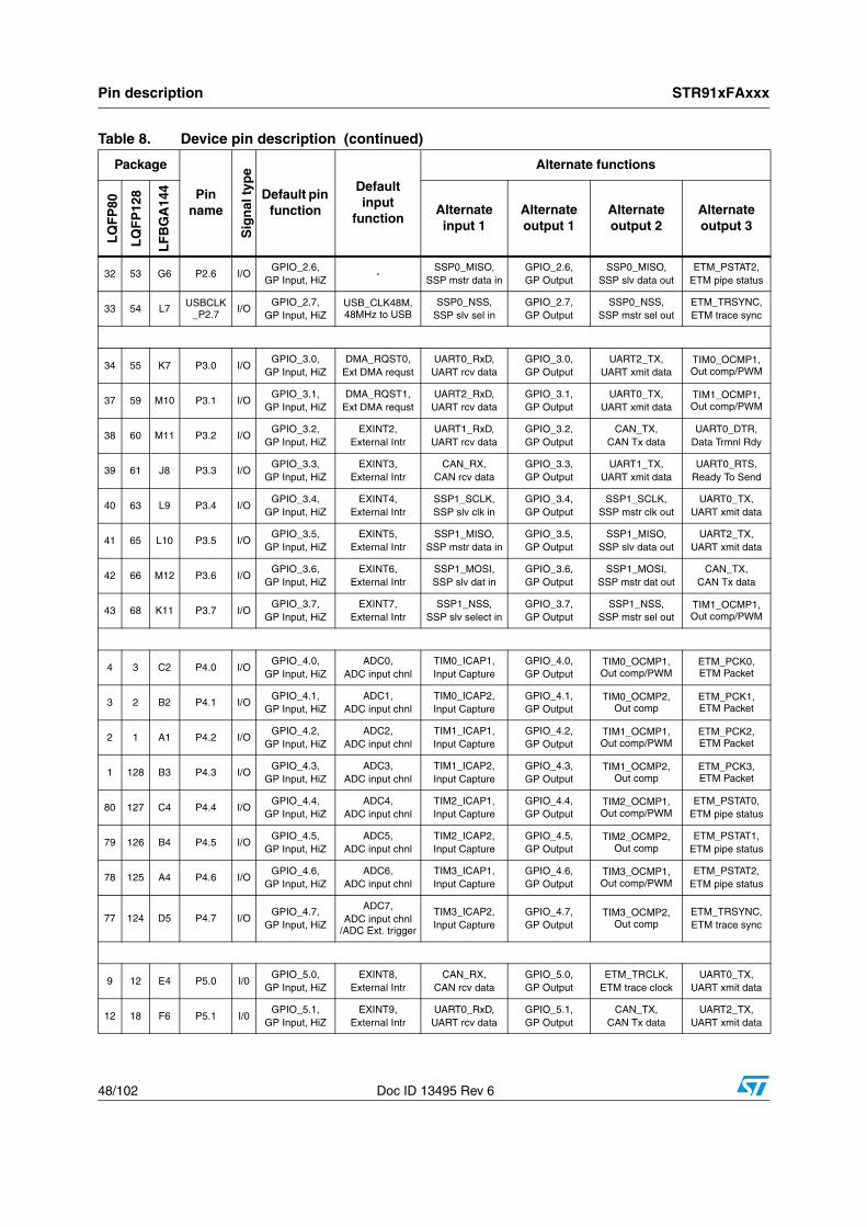
Pin description STR91xFAxxx
48/102 Doc ID 13495 Rev 6
32 53 G6 P2.6 I/OGPIO_2.6,
GP Input, HiZ-
SSP0_MISO,SSP mstr data in
GPIO_2.6, GP Output
SSP0_MISO,SSP slv data out
ETM_PSTAT2,ETM pipe status
33 54 L7 USBCLK_P2.7 I/O
GPIO_2.7,GP Input, HiZ
USB_CLK48M, 48MHz to USB
SSP0_NSS,SSP slv sel in
GPIO_2.7, GP Output
SSP0_NSS,SSP mstr sel out
ETM_TRSYNC,ETM trace sync
34 55 K7 P3.0 I/OGPIO_3.0,
GP Input, HiZDMA_RQST0,
Ext DMA requstUART0_RxD,
UART rcv dataGPIO_3.0, GP Output
UART2_TX,UART xmit data
TIM0_OCMP1, Out comp/PWM
37 59 M10 P3.1 I/OGPIO_3.1,
GP Input, HiZDMA_RQST1,
Ext DMA requstUART2_RxD,
UART rcv dataGPIO_3.1, GP Output
UART0_TX,UART xmit data
TIM1_OCMP1, Out comp/PWM
38 60 M11 P3.2 I/OGPIO_3.2,
GP Input, HiZEXINT2,
External IntrUART1_RxD,
UART rcv dataGPIO_3.2, GP Output
CAN_TX,CAN Tx data
UART0_DTR,Data Trmnl Rdy
39 61 J8 P3.3 I/OGPIO_3.3,
GP Input, HiZEXINT3,
External IntrCAN_RX,
CAN rcv dataGPIO_3.3, GP Output
UART1_TX,UART xmit data
UART0_RTS,Ready To Send
40 63 L9 P3.4 I/OGPIO_3.4,
GP Input, HiZEXINT4,
External IntrSSP1_SCLK,SSP slv clk in
GPIO_3.4, GP Output
SSP1_SCLK,SSP mstr clk out
UART0_TX,UART xmit data
41 65 L10 P3.5 I/OGPIO_3.5,
GP Input, HiZEXINT5,
External IntrSSP1_MISO,
SSP mstr data inGPIO_3.5, GP Output
SSP1_MISO,SSP slv data out
UART2_TX,UART xmit data
42 66 M12 P3.6 I/OGPIO_3.6,
GP Input, HiZEXINT6,
External IntrSSP1_MOSI,SSP slv dat in
GPIO_3.6, GP Output
SSP1_MOSI,SSP mstr dat out
CAN_TX,CAN Tx data
43 68 K11 P3.7 I/OGPIO_3.7,
GP Input, HiZEXINT7,
External IntrSSP1_NSS,
SSP slv select inGPIO_3.7, GP Output
SSP1_NSS,SSP mstr sel out
TIM1_OCMP1, Out comp/PWM
4 3 C2 P4.0 I/OGPIO_4.0,
GP Input, HiZADC0,
ADC input chnl TIM0_ICAP1,Input Capture
GPIO_4.0, GP Output
TIM0_OCMP1, Out comp/PWM
ETM_PCK0, ETM Packet
3 2 B2 P4.1 I/OGPIO_4.1,
GP Input, HiZADC1,
ADC input chnl TIM0_ICAP2,Input Capture
GPIO_4.1, GP Output
TIM0_OCMP2, Out comp
ETM_PCK1, ETM Packet
2 1 A1 P4.2 I/OGPIO_4.2,
GP Input, HiZADC2,
ADC input chnl TIM1_ICAP1,Input Capture
GPIO_4.2, GP Output
TIM1_OCMP1, Out comp/PWM
ETM_PCK2, ETM Packet
1 128 B3 P4.3 I/OGPIO_4.3,
GP Input, HiZADC3,
ADC input chnl TIM1_ICAP2,Input Capture
GPIO_4.3, GP Output
TIM1_OCMP2, Out comp
ETM_PCK3, ETM Packet
80 127 C4 P4.4 I/OGPIO_4.4,
GP Input, HiZADC4,
ADC input chnl TIM2_ICAP1,Input Capture
GPIO_4.4, GP Output
TIM2_OCMP1, Out comp/PWM
ETM_PSTAT0,ETM pipe status
79 126 B4 P4.5 I/OGPIO_4.5,
GP Input, HiZADC5,
ADC input chnl TIM2_ICAP2,Input Capture
GPIO_4.5, GP Output
TIM2_OCMP2, Out comp
ETM_PSTAT1,ETM pipe status
78 125 A4 P4.6 I/OGPIO_4.6,
GP Input, HiZADC6,
ADC input chnl TIM3_ICAP1,Input Capture
GPIO_4.6, GP Output
TIM3_OCMP1, Out comp/PWM
ETM_PSTAT2,ETM pipe status
77 124 D5 P4.7 I/OGPIO_4.7,
GP Input, HiZ
ADC7,ADC input chnl
/ADC Ext. trigger
TIM3_ICAP2,Input Capture
GPIO_4.7, GP Output
TIM3_OCMP2, Out comp
ETM_TRSYNC,ETM trace sync
9 12 E4 P5.0 I/0GPIO_5.0,
GP Input, HiZEXINT8,
External IntrCAN_RX,
CAN rcv dataGPIO_5.0, GP Output
ETM_TRCLK,ETM trace clock
UART0_TX,UART xmit data
12 18 F6 P5.1 I/0GPIO_5.1,
GP Input, HiZEXINT9,
External IntrUART0_RxD,
UART rcv dataGPIO_5.1, GP Output
CAN_TX,CAN Tx data
UART2_TX,UART xmit data
Table 8. Device pin description (continued)
Package
Pin name
Sig
nal
typ
e
Default pin function
Default input
function
Alternate functions
LQ
FP
80
LQ
FP
128
LF
BG
A14
4
Alternate input 1
Alternate output 1
Alternate output 2
Alternate output 3

STR91xFAxxx Pin description
Doc ID 13495 Rev 6 49/102
17 25 K1 PHYCLK_P5.2 I/O
GPIO_5.2,GP Input, HiZ
EXINT10,External Intr
UART2_RxD,UART rcv data
GPIO_5.2, GP Output
MII_PHYCLK, 25Mhz to PHY
TIM3_OCMP1, Out comp/PWM
18 27 H2 P5.3 I/OGPIO_5.3,
GP Input, HiZEXINT11,
External IntrETM_EXTRIG,ETM ext. trigger
GPIO_5.3, GP Output
MII_TX_EN,MAC xmit enbl
TIM2_OCMP1, Out comp/PWM
44 70 J12 P5.4 I/OGPIO_5.4,
GP Input, HiZEXINT12,
External IntrSSP0_SCLK,SSP slv clk in
GPIO_5.4, GP Output
SSP0_SCLK,SSP mstr clk out
EMI_CS0n,EMI Chip Select
47 77 H11 P5.5 I/OGPIO_5.5,
GP Input, HiZEXINT13,
External IntrSSP0_MOSI,SSP slv dat in
GPIO_5.5, GP Output
SSP0_MOSI,SSP mstr dat out
EMI_CS1n,EMI Chip Select
48 79 H9 P5.6 I/OGPIO_5.6,
GP Input, HiZEXINT14,
External IntrSSP0_MISO,
SSP mstr dat inGPIO_5.6, GP Output
SSP0_MISO,SSP slv data out
EMI_CS2n,EMI Chip Select
49 80 G12 P5.7 I/OGPIO_5.7,
GP Input, HiZEXINT15,
External IntrSSP0_NSS,
SSP slv select inGPIO_5.7, GP Output
SSP0_NSS,SSP mstr sel out
EMI_CS3n,EMI Chip Select
19 29 H4 P6.0 I/OGPIO_6.0,
GP Input, HiZEXINT16,
External IntrTIM0_ICAP1,Input Capture
GPIO_6.0, GP Output
TIM0_OCMP1, Out comp/PWM
MC_UH,IMC phase U hi
20 31 J3 P6.1 I/OGPIO_6.1,
GP Input, HiZEXINT17,
External IntrTIM0_ICAP2,Input Capture
GPIO_6.1, GP Output
TIM0_OCMP2, Out comp
MC_UL,IMC phase U lo
13 19 G2 P6.2 I/OGPIO_6.2,
GP Input, HiZEXINT18,
External IntrTIM1_ICAP1,Input Capture
GPIO_6.2, GP Output
TIM1_OCMP1, Out comp/PWM
MC_VH,IMC phase V hi
14 20 G3 P6.3 I/OGPIO_6.3,
GP Input, HiZEXINT19,
External IntrTIM1_ICAP2,Input Capture
GPIO_6.3, GP Output
TIM1_OCMP2, Out comp
MC_VL,IMC phase V lo
52 83 G8 P6.4 I/OGPIO_6.4,
GP Input, HiZEXINT20,
External IntrTIM2_ICAP1,Input Capture
GPIO_6.4, GP Output
TIM2_OCMP1, Out comp/PWM
MC_WH,IMC phase W hi
53 84 G7 P6.5 I/OGPIO_6.5,
GP Input, HiZEXINT21,
External IntrTIM2_ICAP2,Input Capture
GPIO_6.5, GP Output
TIM2_OCMP2, Out comp
MC_WL,IMC phase W lo
57 92 E9 P6.6 I/OGPIO_6.6,
GP Input, HiZEXINT22_TRIG,Ext Intr & Tach
UART0_RxD,UART rcv data
GPIO_6.6, GP Output
TIM3_OCMP1, Out comp/PWM
ETM_TRCLK,ETM trace clock
58 93 D12 P6.7 I/OGPIO_6.7,
GP Input, HiZEXINT23_STOP,Ext Intr & Estop
ETM_EXTRIG,ETM ext. trigger
GPIO_6.7, GP Output
TIM3_OCMP2, Out comp
UART0_TX,UART xmit data
- 5 D1 P7.0 I/OGPIO_7.0,
GP Input, HiZEXINT24,
External IntrTIM0_ICAP1,Input Capture
GPIO_7.0, GP Output
8b) EMI_A0,16b) EMI_A16
ETM_PCK0, ETM Packet
- 6 D2 P7.1 I/OGPIO_7.1,
GP Input, HiZEXINT25,
External IntrTIM0_ICAP2,Input Capture
GPIO_7.1, GP Output
8b) EMI_A1,16b) EMI_A17
ETM_PCK1, ETM Packet
- 7 B1 P7.2 I/OGPIO_7.2,
GP Input, HiZEXINT26,
External IntrTIM2_ICAP1,Input Capture
GPIO_7.2, GP Output
8b) EMI_A2,16b) EMI_A18
ETM_PCK2, ETM Packet
- 13 F1 P7.3 I/OGPIO_7.3,
GP Input, HiZEXINT27,
External IntrTIM2_ICAP2,Input Capture
GPIO_7.3, GP Output
8b) EMI_A3,16b) EMI_A19
ETM_PCK3, ETM Packet
- 14 G1 P7.4 I/OGPIO_7.4,
GP Input, HiZEXINT28,
External IntrUART0_RxD,
UART rcv dataGPIO_7.4, GP Output
8b) EMI_A4,16b) EMI_A20
EMI_CS3n,EMI Chip Select
- 15 E5 P7.5 I/OGPIO_7.5,
GP Input, HiZEXINT29,
External IntrETM_EXTRIG,ETM ext. trigger
GPIO_7.5, GP Output
8b) EMI_A5,16b) EMI_A21
EMI_CS2n,EMI Chip Select
- 118 E6 P7.6 I/OGPIO_7.6,
GP Input, HiZEXINT30,
External IntrTIM3_ICAP1,Input Capture
GPIO_7.6, GP Output
8b) EMI_A6,16b) EMI_A22
EMI_CS1n,EMI Chip Select
Table 8. Device pin description (continued)
Package
Pin name
Sig
nal
typ
e
Default pin function
Default input
function
Alternate functions
LQ
FP
80
LQ
FP
128
LF
BG
A14
4
Alternate input 1
Alternate output 1
Alternate output 2
Alternate output 3

Pin description STR91xFAxxx
50/102 Doc ID 13495 Rev 6
- 119 A5 P7.7 I/OGPIO_7.7,
GP Input, HiZEXINT31,
External IntrTIM3_ICAP2,Input Capture
GPIO_7.7, GP Output
EMI_CS0n,EMI chip select
16b) EMI_A23,8b) EMI_A7
- 26 L1 P8.0 I/OGPIO_8.0,
GP Input, HiZ- -
GPIO_8.0, GP Output
8b) EMI_D0,16b) EMI_AD0
-
- 28 H3 P8.1 I/OGPIO_8.1,
GP Input, HiZ- -
GPIO_8.1, GP Output
8b) EMI_D1,16b) EMI_AD1
-
- 30 J2 P8.2 I/OGPIO_8.2,
GP Input, HiZ- -
GPIO_8.2, GP Output
8b) EMI_D2,16b) EMI_AD2
-
- 32 K2 P8.3 I/OGPIO_8.3,
GP Input, HiZ- -
GPIO_8.3, GP Output
8b) EMI_D3,16b) EMI_AD3
-
- 34 L3 P8.4 I/OGPIO_8.4,
GP Input, HiZ- -
GPIO_8.4, GP Output
8b) EMI_D4,16b) EMI_AD4
-
- 36 J4 P8.5 I/OGPIO_8.5,
GP Input, HiZ- -
GPIO_8.5, GP Output
8b) EMI_D5,16b) EMI_AD5
-
- 38 M2 P8.6 I/OGPIO_8.6,
GP Input, HiZ- -
GPIO_8.6, GP Output
8b) EMI_D6,16b) EMI_AD6
-
- 44 K5 P8.7 I/OGPIO_8.7,
GP Input, HiZ- -
GPIO_8.7, GP Output
8b) EMI_D7,16b) EMI_AD7
-
- 46 M6 P9.0 I/OGPIO_9.0,
GP Input, HiZ- -
GPIO_9.0, GP Output
8b) EMI_A816b) EMI_AD8
-
- 47 M7 P9.1 I/OGPIO_9.1,
GP Input, HiZ- -
GPIO_9.1, GP Output
8b) EMI_A9,16b) EMI_AD9
-
- 50 K6 P9.2 I/OGPIO_9.2,
GP Input, HiZ- -
GPIO_9.2, GP Output
8b) EMI_A10,16b)EMI_AD10
-
- 51 J6 P9.3 I/OGPIO_9.3,
GP Input, HiZ- -
GPIO_9.3, GP Output
8b) EMI_A11,16b)EMI_AD11
-
- 52 H6 P9.4 I/OGPIO_9.4,
GP Input, HiZ- -
GPIO_9.4, GP Output
8b) EMI_A12,16b)EMI_AD12
-
- 58 L8 P9.5 I/OGPIO_9.5,
GP Input, HiZ- -
GPIO_9.5, GP Output
8b) EMI_A13,16b)EMI_AD13
-
- 62 M9 P9.6 I/OGPIO_9.6,
GP Input, HiZ- -
GPIO_9.6, GP Output
8b) EMI_A14,16b)EMI_AD14
-
- 64 K9 P9.7 I/OGPIO_9.7,
GP Input, HiZ- -
GPIO_9.7, GP Output
8b) EMI_A15,16b)EMI_AD15
-
- 21 G4EMI_
BWR_WRLn
O
EMI byte write strobe (8 bit mode) or low
byte write strobe (16 bit
mode)Can also be
configured as EMI_LBn in
BGA package
N/A
Table 8. Device pin description (continued)
Package
Pin name
Sig
nal
typ
e
Default pin function
Default input
function
Alternate functions
LQ
FP
80
LQ
FP
128
LF
BG
A14
4
Alternate input 1
Alternate output 1
Alternate output 2
Alternate output 3

STR91xFAxxx Pin description
Doc ID 13495 Rev 6 51/102
- 22 H1 EMI_WRHn O
EMI high byte write strobe
(16-bit mode)Can also be
configured as EMI_UBn in
BGA package
N/A
- 74 J10 EMI_ALE OEMI address latch enable (mux mode)
N/A
- 75 J9 EMI_RDn O EMI read
strobe N/A
- - H8 EMI_BAAn O
EMI Burst address advance
N/A
- - K8 EMI_WAITn I
EMI Wait input for burst mode
deviceN/A
- - M8 EMI_BCLK O EMI bus clock N/A
- - A12 EMI_WEn O EMI write
enable N/A
- 91 E10 TAMPER_IN I Tamper
detection input N/A
- 94 D11 MII_MDIO I/O
MAC/PHY management
data lineN/A
59 95 D10 USBDN I/O USB data (-) bus connect N/A
60 96 C11 USBDP I/O USB data (+) bus connect N/A
56 89 C12 RESET_INn I External reset
input N/A
62 100 A9 RESET_OUTn O
Global or System reset
outputN/A
65 104 A10 X1_CPU I CPU oscillator or crystal input N/A
64 103 A11 X2_CPU O CPU crystal connection N/A
27 42 M5 X1_RTC IRTC oscillator or crystal input (32.768 kHz)
N/A
26 41 M4 X2_RTC O RTC crystal connection N/A
61 97 B11 JRTCK OJTAG return clock or RTC
clockN/A
67 107 D8 JTRSTn I JTAG TAP controller reset N/A
Table 8. Device pin description (continued)
Package
Pin name
Sig
nal
typ
e
Default pin function
Default input
function
Alternate functions
LQ
FP
80
LQ
FP
128
LF
BG
A14
4
Alternate input 1
Alternate output 1
Alternate output 2
Alternate output 3
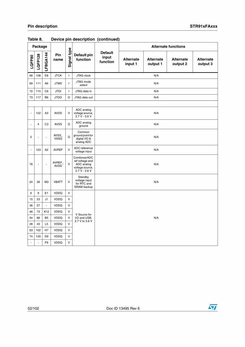
Pin description STR91xFAxxx
52/102 Doc ID 13495 Rev 6
68 108 E8 JTCK I JTAG clock N/A
69 111 A6 JTMS I JTAG mode select N/A
72 115 C6 JTDI I JTAG data in N/A
73 117 B6 JTDO O JTAG data out N/A
- 122 A3 AVDD VADC analog
voltage source, 2.7 V - 3.6 V
N/A
- 4 C3 AVSS G ADC analog ground N/A
5 - - AVSS_VSSQ G
Common ground point for
digital I/O & analog ADC
N/A
- 123 A2 AVREF V ADC reference voltage input N/A
76 - - AVREF_AVDD V
Combined ADC ref voltage and
ADC analog voltage source,
2.7 V - 3.6 V
N/A
24 39 M3 VBATT V
Standby voltage input for RTC and
SRAM backup
N/A
6 9 E1 VDDQ V
V Source forI/O and USB.2.7 V to 3.6 V
N/A
15 23 J1 VDDQ V
36 57 - VDDQ V
46 73 K12 VDDQ V
54 86 B5 VDDQ V
28 43 L5 VDDQ V
63 102 H7 VDDQ V
74 120 D9 VDDQ V
- - F9 VDDQ V
Table 8. Device pin description (continued)
Package
Pin name
Sig
nal
typ
e
Default pin function
Default input
function
Alternate functions
LQ
FP
80
LQ
FP
128
LF
BG
A14
4
Alternate input 1
Alternate output 1
Alternate output 2
Alternate output 3

STR91xFAxxx Pin description
Doc ID 13495 Rev 6 53/102
- 8 L2 VSSQ G
Digital Ground for
!/O and USBN/A
16 24 K4 VSSQ G
35 56 C5 VSSQ G
- - D4 VSSQ G
45 72 G5 VSSQ G
55 87 J7 VSSQ G
25 40 A8 VSSQ G
66 105 F8 VSSQ G
75 121 L12 VSSQ G
11 17 F4 VDD V
V Source for CPU.
1.65 V - 2.0 VN/A
31 49 D7 VDD V
50 81 L6 VDD V
70 112 G11 VDD V
10 16 F3 VSS G
Digital Ground for CPU N/A
30 48 H5 VSS G
51 82 G10 VSS G
71 113 E7 VSS G
- - C9 PLLVDDQ V
V Source for PLL
2.7 to 3.6 V N/A
- - B8 PLLVSSQ G Digital Ground
for PLL
Table 8. Device pin description (continued)
Package
Pin name
Sig
nal
typ
e
Default pin function
Default input
function
Alternate functions
LQ
FP
80
LQ
FP
128
LF
BG
A14
4
Alternate input 1
Alternate output 1
Alternate output 2
Alternate output 3

Memory mapping STR91xFAxxx
54/102 Doc ID 13495 Rev 6
6 Memory mapping
The ARM966E-S CPU addresses a single linear address space of 4 giga-bytes (232) from address 0x0000.0000 to 0xFFFF.FFFF as shown in Figure 9. Upon reset the CPU boots from address 0x0000.0000, which is chip-select zero at address zero in the Flash Memory Interface (FMI).
The Instruction TCM and Data TCM enable high-speed CPU operation without incurring any performance or power penalties associated with accessing the system buses (AHB and APB). I-TCM and D-TCM address ranges are shown at the bottom of the memory map in Figure 9.
6.1 Buffered and non-buffered writesThe CPU makes use of write buffers on the AHB and the D-TCM to decouple the CPU from any wait states associated with a write operation. The user may choose to use write with buffers on the AHB by setting bit 3 in control register CP15 and selecting the appropriate AHB address range when writing. By default at reset, buffered writes are disabled (bit 3 of CP15 is clear) and all AHB writes are non-buffered until enabled. Figure 9 shows that most addressable items on the AHB are aliased at two address ranges, one for buffered writes and another for non-buffered writes. A buffered write will allow the CPU to continue program execution while the write-back is performed through a FIFO to the final destination on the AHB. If the FIFO is full, the CPU is stalled until FIFO space is available. A non-buffered write will impose an immediate delay to the CPU, but results in a direct write to the final AHB destination, ensuring data coherency. Read operations from AHB locations are always direct and never buffered.
6.2 System (AHB) and peripheral (APB) busesThe CPU will access SRAM, higher-speed peripherals (USB, Ethernet, Programmable DMA), and the external bus (EMI) on the AHB at their respective base addresses indicated in Figure 9. Lower-speed peripherals reside on the APB and are accessed using two separate AHB-to-APB bridge units (APB0 and APB1). These bridge units are essentially address windows connecting the AHB to the APB. To access an individual APB peripheral, the CPU will place an address on the AHB bus equal to the base address of the appropriate bridge unit APB0 or APB1, plus the offset of the particular peripheral, plus the offset of the individual data location within the peripheral. Figure 9 shows the base addresses of bridge units APB0 and APB1, and also the base address of each APB peripheral. Please consult the STR91xFA Reference manual for the address of data locations within each individual peripheral.
STR91xFAxxx Memory mapping
Doc ID 13495 Rev 6 55/102
6.3 SRAMThe SRAM is aliased at three separate address ranges as shown in Figure 9. When the CPU accesses SRAM starting at 0x0400.0000, the SRAM appears on the D-TCM. When CPU access starts at 0x4000.0000, SRAM appears in the buffered AHB range. Beginning at CPU address 0x5000.0000, SRAM is in non-buffered AHB range. The SRAM size must be specified by CPU intitialization firmware writing to a control register after any reset condition. Default SRAM size is 32K bytes, with option to set to 64K bytes on STR91xFAx3x devices, and to 96K bytes on STR91xFAx4x devices.
When other AHB bus masters (such as a DMA controller) write to SRAM, their access is never buffered. Only the CPU can make use of buffered AHB writes.
6.4 Two independent Flash memoriesThe STR91xFA has two independent Flash memories, the larger primary Flash and the small secondary Flash. It is possible for the CPU to erase/write to one of these Flash memories while simultaneously reading from the other.
One or the other of these two Flash memories may reside at the “boot” address position of 0x0000.0000 at power-up or at reset as shown in Figure 9. The default configuration is that the first sector of primary Flash memory is enabled and residing at the boot position, and the secondary Flash memory is disabled. This default condition may be optionally changed as described below.
6.4.1 Default configuration
When the primary Flash resides at boot position, typical CPU initialization firmware would set the start address and size of the main Flash memory, and go on to enable the secondary Flash, define it’s start address and size. Most commonly, firmware would place the secondary Flash start address at the location just after the end of the primary Flash memory. In this case, the primary Flash is used for code storage, and the smaller secondary Flash can be used for data storage (EEPROM emulation).
6.4.2 Optional configuration
Using the STR91xFA device configuration software tool, or IDE from 3rd party, one can specify that the smaller secondary Flash memory is at the boot location at reset and the primary Flash is disabled. The selection of which Flash memory is at the boot location is programmed in a non-volatile Flash-based configuration bit during JTAG ISP. The boot selection choice will remain as the default until the bit is erased and re-written by the JTAG interface. The CPU cannot change this choice for boot Flash, only the JTAG interface has access.
In this case where the secondary Flash defaults to the boot location upon reset, CPU firmware would typically initialize the Flash memories the following way. The secondary Flash start address and size is specified, then the primary Flash is enabled and its start address and size is specified. The primary Flash start address would typically be located just after the final address location of the secondary Flash. This configuration is particularly well-suited for In-Application-Programming (IAP). The CPU would boot from the secondary Flash memory, initialize the system, then check the contents of the primary Flash memory (by checksum or other means). If the contents of primary Flash is OK, then CPU execution continues from either Flash memory.

Memory mapping STR91xFAxxx
56/102 Doc ID 13495 Rev 6
If the main Flash contents are incorrect, the CPU, while executing code from the secondary Flash, can download new data from any STR91xFA communication channel and program into primary Flash memory. Application code then starts after the new contents of primary Flash are verified.
6.5 STR91xFA memory mapThe memory map is shown in Figure 9: STR91xFA memory map on page 57:
Either of the two Flash memories may be placed at CPU boot address 0x0000.0000. By default, the primary Flash memory is in boot position starting at CPU address 0x0000.0000 and the secondary Flash memory may be placed at a higher address following the end of the primary Flash memory. This default option may be changed using the STR91xx device configuration software, placing the secondary Flash memory at CPU boot location 0x0000.0000, and then the primary Flash memory may be placed at a higher address.
The local SRAM (64KB or 96KB) is aliased in three address windows. A) At 0x0400.0000 the SRAM is accessible through the CPU’s D-TCM, at 0x4000.0000 the SRAM is accessible through the CPU’s AHB in buffered accesses, and at 0x5000.0000 the SRAM is accessible through the CPU’s AHB in non-buffered accesses. An AHB bus master other than the CPU can access SRAM in all three aliased windows, but these accesses are always non-buffered. The CPU is the only AHB master that can performed buffered writes.
APB peripherals reside in two AHB-to-APB peripheral bridge address windows, APB0 and APB1. These peripherals are accessible with buffered AHB access if the CPU addresses them in the address range of 0x4800.0000 to 0x4FFF.FFFF, and non-buffered access in the address range of 0x5800.0000 to 0x5FFF.FFFF.
Individual peripherals on the APB are accessed at the listed address offset plus the base address of the appropriate AHB-to-APB bridge.
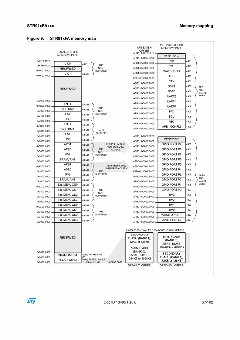
STR91xFAxxx Memory mapping
Doc ID 13495 Rev 6 57/102
Figure 9. STR91xFA memory map
0x0000.0000FLASH, I-TCM
SRAM, D-TCM0x0400.0000
0x2000.0000
Using 288 KB, 544 KB,1.1 MB or 2.1 MB
Using 64 KB or 96KB
0x0800.0000
RESERVED
Ext. MEM, CS3
Ext. MEM, CS2
Ext. MEM, CS1
Ext. MEM, CS0
64 MB
64 MB
64 MB
64 MB
0x2400.0000
0x2800.0000
0x2C00.0000
AHBBUFFERED
0x3000.0000Ext. MEM, CS3
Ext. MEM, CS2
Ext. MEM, CS1
Ext. MEM, CS0
64 MB
64 MB
64 MB
64 MB
0x3400.0000
0x3800.0000
0x3C00.0000AHBNON-
BUFFERED
0x4000.0000SRAM, AHB
FMI
APB0
APB1
64 MB
64 MB
64 MB
64 MB
0x4400.0000
0x4800.0000
0x4C00.0000
AHBBUFFERED
0x5000.0000SRAM, AHB
FMI
APB0
APB1
64 MB
64 MB
64 MB
64 MB
0x5400.0000
0x5800.0000
0x5C00.0000AHBNON-
BUFFERED
0x6000.0000USB
EMI
8-CH DMA
ENET
64 MB
64 MB
64 MB
64 MB
0x6400.0000
0x6800.0000
0x6C00.0000
AHBBUFFERED
0x7000.0000USB
EMI
8-CH DMA
ENET
64 MB
64 MB
64 MB
64 MB
0x7400.0000
0x7800.0000
0x7C00.0000
RESERVED
VIC1
VIC0
0x8000.0000
0xFC00.0000
0xFC01.0000
0xFFFF.F000
0xFFFF.FFFF4 KB
64 KB
AHBNON-
BUFFERED
AHBNON-
BUFFERED
4 KBI2C1
4 KBAPB0 CONFIG
4 KBWAKE-UP UNIT
4 KB
GPIO PORT P0
4 KB
GPIO PORT P1
4 KB
GPIO PORT P2
4 KB
GPIO PORT P3
4 KB
GPIO PORT P4
4 KB
GPIO PORT P5
4 KB
GPIO PORT P6
4 KB
GPIO PORT P7
4 KB
GPIO PORT P8
4 KB
GPIO PORT P9
4 KB
TIM0
4 KB
TIM1
4 KB
TIM2
4 KB
TIM3
4 KBAPB1 CONFIG
4 KBRTC
4 KBSCU
4 KBIMC
4 KBUART0
4 KBUART1
4 KBUART2
4 KBSSP0
4 KBSSP1
4 KBCAN
4 KBADC
4 KBWATCHDOG
4 KBI2C0
RESERVED
APB0+0x0000.0000
PERIPHERAL BUSMEMORY SPACE
RESERVED
APB0+0x0000.1000
APB0+0x0000.2000
APB0+0x0000.3000
APB0+0x0000.4000
APB0+0x0000.5000
APB0+0x0000.6000
APB0+0x0000.7000
APB0+0x0000.8000
APB0+0x0000.9000
APB0+0x0000.A000
APB0+0x0000.B000
APB0+0x0000.C000
APB0+0x0000.D000
APB0+0x0000.E000
APB0+0x0000.F000
APB1+0x0000.1000
APB1+0x0000.2000
APB1+0x0000.3000
APB1+0x0000.4000
APB1+0x0000.5000
APB1+0x0000.6000
APB1+0x0000.7000
APB1+0x0000.8000
APB1+0x0000.9000
APB1+0x0000.A000
APB1+0x0000.B000
APB1+0x0000.C000
APB1+0x0000.D000
APB1+0x0000.E000
APB1+0x03FF.FFFF
RESERVED
PERIPHERAL BUS,NON- BUFFERED
ACCESS
PERIPHERAL BUS,BUFFERED ACCESS
TOTAL 4 GB CPUMEMORY SPACE
0x0000.0000
MAIN FLASH(BANK 0),
256KB, 512KB,1024KB or 2028KB
SECONDARYFLASH (BANK 1),
32KB or 128KB
MAIN FLASH(BANK 0),
256KB, 512KB,1024KB or 2048KB
SECONDARYFLASH (BANK 1),
32KB or 128KB
Order of the two Flash memories is user defined.
DEFAULT ORDER OPTIONAL ORDER
APB1+0x0000.0000
APB0+0x0001.0000
APB0+0x03FF.FFFF
APB BASE +OFFSET
APB1,AHB-to-APBBridge
APB0,AHB-to-APBBridge

Electrical characteristics STR91xFAxxx
58/102 Doc ID 13495 Rev 6
7 Electrical characteristics
7.1 Parameter conditionsUnless otherwise specified, all voltages are referred to VSS.
7.1.1 Minimum and maximum values
Unless otherwise specified the minimum and maximum values are guaranteed in the worst conditions of ambient temperature, supply voltage and frequencies by tests in production on 100% of the devices with an ambient temperature at TAmax (given by the selected temperature range).
Data based on product characterisation, design simulation and/or technology characteristics are indicated in the table footnotes and are not tested in production. Based on characterization, the minimum and maximum values refer to sample tests and represent the mean value plus or minus three times the standard deviation (mean±3Σ).
7.1.2 Typical values
Unless otherwise specified, typical data are based on TA = 25° C, VDDQ = 3.3 V and VDD=1.8 V. They are given only as design guidelines and are not tested.
Typical ADC accuracy values are determined by characterization of a batch of samples from a standard diffusion lot over the full temperature range, where 95% of the devices have an error less than or equal to the value indicated (mean ± 2 Σ).
7.1.3 Typical curves
Unless otherwise specified, all typical curves are given only as design guidelines and are not tested.
7.1.4 Loading capacitor
The loading conditions used for pin parameter measurement are shown in Figure 10.
Figure 10. Pin loading conditions
7.1.5 Pin input voltage
The input voltage measurement on a pin of the device is described in Figure 11.
CL=50pF
STR9 PIN
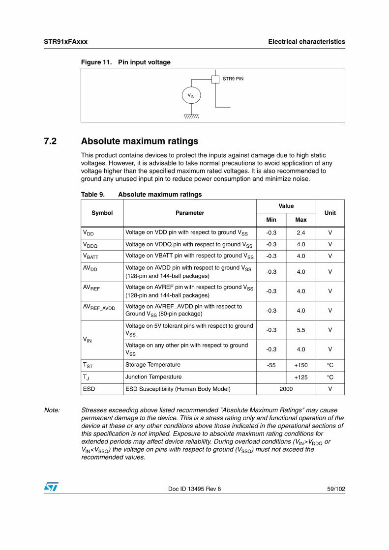
STR91xFAxxx Electrical characteristics
Doc ID 13495 Rev 6 59/102
Figure 11. Pin input voltage
7.2 Absolute maximum ratingsThis product contains devices to protect the inputs against damage due to high static voltages. However, it is advisable to take normal precautions to avoid application of any voltage higher than the specified maximum rated voltages. It is also recommended to ground any unused input pin to reduce power consumption and minimize noise.
Note: Stresses exceeding above listed recommended "Absolute Maximum Ratings" may cause permanent damage to the device. This is a stress rating only and functional operation of the device at these or any other conditions above those indicated in the operational sections of this specification is not implied. Exposure to absolute maximum rating conditions for extended periods may affect device reliability. During overload conditions (VIN>VDDQ or VIN<VSSQ) the voltage on pins with respect to ground (VSSQ) must not exceed the recommended values.
VIN
STR9 PIN
Table 9. Absolute maximum ratings
Symbol ParameterValue
UnitMin Max
VDD Voltage on VDD pin with respect to ground VSS -0.3 2.4 V
VDDQ Voltage on VDDQ pin with respect to ground VSS -0.3 4.0 V
VBATT Voltage on VBATT pin with respect to ground VSS -0.3 4.0 V
AVDD Voltage on AVDD pin with respect to ground VSS
(128-pin and 144-ball packages)-0.3 4.0 V
AVREF Voltage on AVREF pin with respect to ground VSS (128-pin and 144-ball packages)
-0.3 4.0 V
AVREF_AVDD Voltage on AVREF_AVDD pin with respect to Ground VSS (80-pin package) -0.3 4.0 V
VIN
Voltage on 5V tolerant pins with respect to ground VSS
-0.3 5.5 V
Voltage on any other pin with respect to ground VSS
-0.3 4.0 V
TST Storage Temperature -55 +150 °C
TJ Junction Temperature +125 °C
ESD ESD Susceptibility (Human Body Model) 2000 V

Electrical characteristics STR91xFAxxx
60/102 Doc ID 13495 Rev 6
Table 10. Current characteristics
Symbol Ratings Maximum
valueUnit
IVDD_IO(1)
1. The user can use GPIOs to source or sink current. In this case, the user must ensure that these absolute max. values are not exceeded (taking into account the RUN power consumption).
Total current into VDD_IO power lines (source) (2)
2. All 3.3 V or 5.0 V power (VDD_IO, VDDA_ADC, VDDA_PLL) and ground (VSS_IO, VSSA_ADC, VDDA_ADC) pins must always be connected to the external 3.3V or 5.0V supply.
200
mAIVSS_IO
(1) Total current out of VSS ground lines (sink) (2) 200
IIOOutput current sunk by any I/O and control pin 25
Output current source by any I/Os and control pin - 25
IINJ(PIN)(3)
3. IINJ(PIN) must never be exceeded. This is implicitly insured if VIN maximum is respected. If VIN maximum cannot be respected, the injection current must be limited externally to the IINJ(PIN) value. A positive injection is induced by VIN>VDD while a negative injection is induced by VIN<VSS.
Injected current on any pin during overload condition(4)
4. When several inputs are submitted to a current injection, the maximum ΣIINJ(PIN) is the absolute sum of the positive and negative injected currents (instantaneous values). These results are based on characterization with ΣIINJ(PIN) maximum current injection on four I/O port pins of the device.
± 5
mAΣIINJ(PIN)
(3) Absolute sum of all input currents during overload condition
(4) ± 25

STR91xFAxxx Electrical characteristics
Doc ID 13495 Rev 6 61/102
7.3 Operating conditions
7.3.1 Operating conditions at power-up / power-down
Subject to general operating conditions for TA.
Table 11. Operating conditions
Symbol Parameter ConditionsValue
UnitMin Max
VDD Digital CPU supply voltage
Flash size ≤ 512 KB 1.65 2.0 V
Flash size = 1 MB / 2 MB,
fCPUCLK ≤ 85 MHz (1) 1.65 2.0 V
Flash size = 1 MB / 2 MB,
fCPUCLK ≤ 96 MHz (2) 1.77 2.0 V
VDDQ Digital I/O supply voltage 2.7 3.6 V
VBATT(3) SRAM backup and RTC supply
voltage2.5 3.6 V
AVDDAnalog ADC supply voltage (128-pin and 144-ball packages)
2.7 VDDQ V
AVREFAnalog ADC reference voltage (128-pin and 144-ball packages)
2.65 AVDD(4) V
AVREF_AVDD
Combined analog ADC reference and ADC supply voltage (80-pin package)
2.7 VDDQ V
TA Ambient temperature under bias -40 +85 C
1. fFMICLK ≤ 48 MHz during Flash write and 85 MHz during all other operations.
2. fFMICLK ≤ 48 MHz during Flash write and 96 MHz during all other operations.
3. The VBATT pin should be connected to VDDQ if no battery is installed
4. AVREF must never exceed VDDQ
Table 12. Operating conditions at power-up / power-down
Symbol Parameter Min(1)
1. Data guaranteed by characterization, not tested in production.
Max(1) Unit
tVDD VDD rise time rate 10 µs/V
10 ms/V
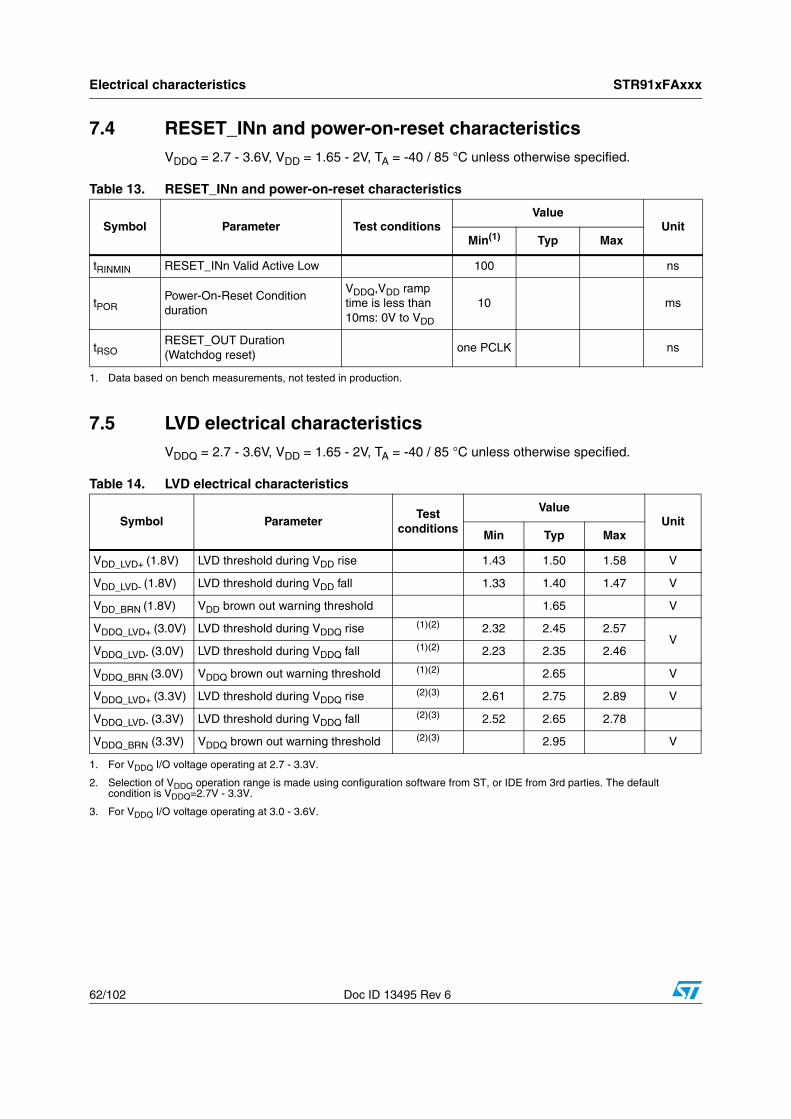
Electrical characteristics STR91xFAxxx
62/102 Doc ID 13495 Rev 6
7.4 RESET_INn and power-on-reset characteristicsVDDQ = 2.7 - 3.6V, VDD = 1.65 - 2V, TA = -40 / 85 °C unless otherwise specified.
7.5 LVD electrical characteristicsVDDQ = 2.7 - 3.6V, VDD = 1.65 - 2V, TA = -40 / 85 °C unless otherwise specified.
Table 13. RESET_INn and power-on-reset characteristics
Symbol Parameter Test conditionsValue
UnitMin(1) Typ Max
tRINMIN RESET_INn Valid Active Low 100 ns
tPORPower-On-Reset Condition duration
VDDQ,VDD ramp time is less than 10ms: 0V to VDD
10 ms
tRSORESET_OUT Duration(Watchdog reset)
one PCLK ns
1. Data based on bench measurements, not tested in production.
Table 14. LVD electrical characteristics
Symbol ParameterTest
conditions
ValueUnit
Min Typ Max
VDD_LVD+ (1.8V) LVD threshold during VDD rise 1.43 1.50 1.58 V
VDD_LVD- (1.8V) LVD threshold during VDD fall 1.33 1.40 1.47 V
VDD_BRN (1.8V) VDD brown out warning threshold 1.65 V
VDDQ_LVD+ (3.0V) LVD threshold during VDDQ rise (1)(2) 2.32 2.45 2.57V
VDDQ_LVD- (3.0V) LVD threshold during VDDQ fall (1)(2) 2.23 2.35 2.46
VDDQ_BRN (3.0V) VDDQ brown out warning threshold (1)(2) 2.65 V
VDDQ_LVD+ (3.3V) LVD threshold during VDDQ rise (2)(3) 2.61 2.75 2.89 V
VDDQ_LVD- (3.3V) LVD threshold during VDDQ fall (2)(3) 2.52 2.65 2.78
VDDQ_BRN (3.3V) VDDQ brown out warning threshold (2)(3) 2.95 V
1. For VDDQ I/O voltage operating at 2.7 - 3.3V.
2. Selection of VDDQ operation range is made using configuration software from ST, or IDE from 3rd parties. The default condition is VDDQ=2.7V - 3.3V.
3. For VDDQ I/O voltage operating at 3.0 - 3.6V.
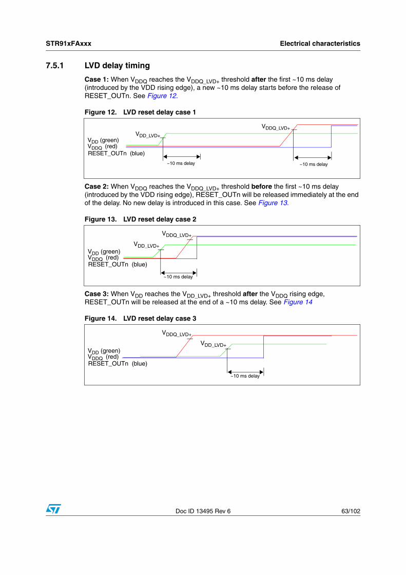
STR91xFAxxx Electrical characteristics
Doc ID 13495 Rev 6 63/102
7.5.1 LVD delay timing
Case 1: When VDDQ reaches the VDDQ_LVD+ threshold after the first ~10 ms delay (introduced by the VDD rising edge), a new ~10 ms delay starts before the release of RESET_OUTn. See Figure 12.
Figure 12. LVD reset delay case 1
Case 2: When VDDQ reaches the VDDQ_LVD+ threshold before the first ~10 ms delay (introduced by the VDD rising edge), RESET_OUTn will be released immediately at the end of the delay. No new delay is introduced in this case. See Figure 13.
Figure 13. LVD reset delay case 2
Case 3: When VDD reaches the VDD_LVD+ threshold after the VDDQ rising edge, RESET_OUTn will be released at the end of a ~10 ms delay. See Figure 14
Figure 14. LVD reset delay case 3
VDD_LVD+
VDDQ_LVD+
~10 ms delay ~10 ms delay
VDDQ (red)RESET_OUTn (blue)
VDD (green)
VDD_LVD+
VDDQ_LVD+
~10 ms delay
VDDQ (red)RESET_OUTn (blue)
VDD (green)
VDD_LVD+
VDDQ_LVD+
~10 ms delay
VDDQ (red)RESET_OUTn (blue)
VDD (green)
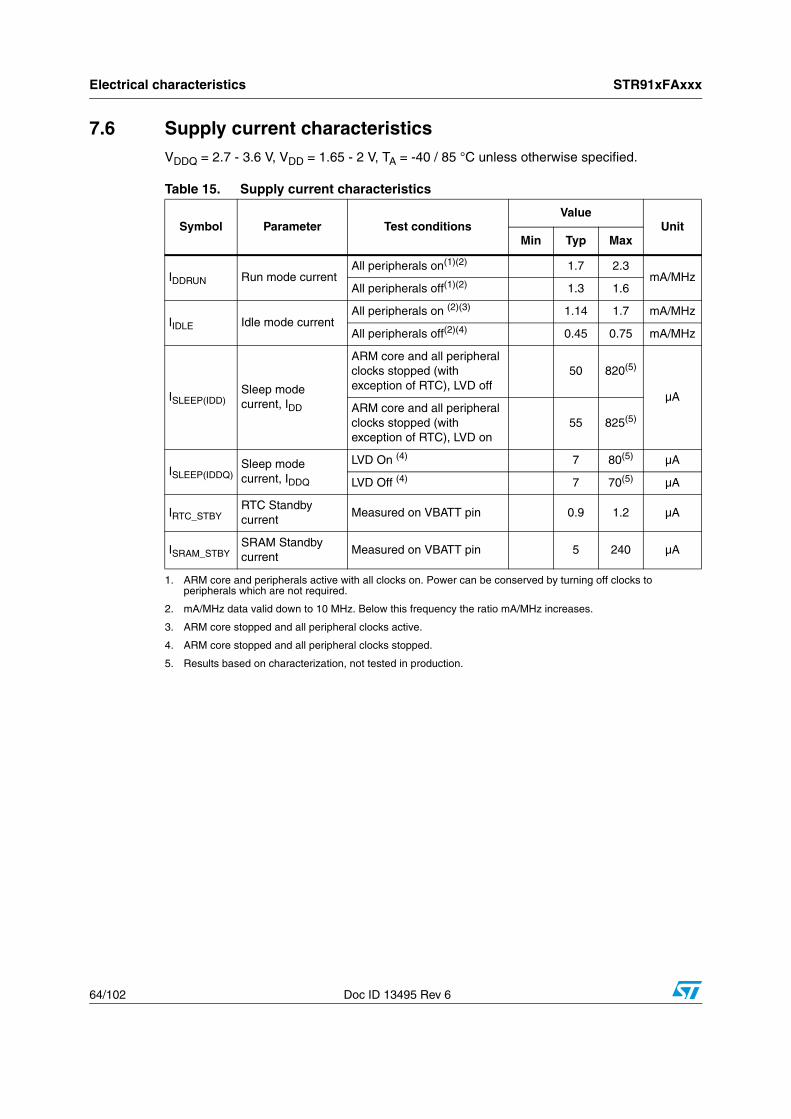
Electrical characteristics STR91xFAxxx
64/102 Doc ID 13495 Rev 6
7.6 Supply current characteristicsVDDQ = 2.7 - 3.6 V, VDD = 1.65 - 2 V, TA = -40 / 85 °C unless otherwise specified.
Table 15. Supply current characteristics
Symbol Parameter Test conditionsValue
UnitMin Typ Max
IDDRUN Run mode currentAll peripherals on(1)(2)
1. ARM core and peripherals active with all clocks on. Power can be conserved by turning off clocks to peripherals which are not required.
2. mA/MHz data valid down to 10 MHz. Below this frequency the ratio mA/MHz increases.
1.7 2.3mA/MHz
All peripherals off(1)(2) 1.3 1.6
IIDLE Idle mode currentAll peripherals on (2)(3)
3. ARM core stopped and all peripheral clocks active.
1.14 1.7 mA/MHz
All peripherals off(2)(4)
4. ARM core stopped and all peripheral clocks stopped.
0.45 0.75 mA/MHz
ISLEEP(IDD)Sleep mode current, IDD
ARM core and all peripheral clocks stopped (with exception of RTC), LVD off
50 820(5)
µAARM core and all peripheral clocks stopped (with exception of RTC), LVD on
55 825(5)
ISLEEP(IDDQ)Sleep mode current, IDDQ
LVD On (4) 7 80(5)
5. Results based on characterization, not tested in production.
µA
LVD Off (4) 7 70(5) µA
IRTC_STBYRTC Standby current
Measured on VBATT pin 0.9 1.2 µA
ISRAM_STBYSRAM Standby current
Measured on VBATT pin 5 240 µA

STR91xFAxxx Electrical characteristics
Doc ID 13495 Rev 6 65/102
Figure 15. Sleep mode current vs temperature with LVD on
7.6.1 Typical power consumption for frequencies below 10 MHz
The following conditions apply to Table 16:
Program is executed from Flash. The program consists of an infinite loop.
A standard crystal source is used.
The PLL is off.
All clock dividers are with their default values.
0
200
400
600
800
1000
1200
1400
1600
1800
2000
0 20 40 60 80 100 120-20-40
Idd
[µA
]
TEMP [°C]
VDD = 1.8 V
VDD = 2.0 V
Table 16. Typical current consumption at 25 °C
Symbol Parameter Test conditionsTypical current on VDD (1.8 V)
Unit
IDDRUNRun mode
current
All peripherals
ON
fMSTR=fOSC=fPCLK=fHCLK=1 MHz 2.88
mA
fMSTR=fOSC=fPCLK=fHCLK=2 MHz 5.8
fMSTR=fOSC=fPCLK=fHCLK=4 MHz 10.91
fMSTR=fOSC=fPCLK=fHCLK=6 MHz 15.97
fMSTR=fOSC=fPCLK=fHCLK=8 MHz 20.68
fMSTR=fOSC=fPCLK=fHCLK=10 MHz 25.13
All peripherals
OFF
fMSTR=fOSC=fPCLK=fHCLK=1 MHz 1.8
fMSTR=fOSC=fPCLK=fHCLK=2 MHz 3.62
fMSTR=fOSC=fPCLK=fHCLK=4 MHz 6.71
fMSTR=fOSC=fPCLK=fHCLK=6 MHz 9.81
fMSTR=fOSC=fPCLK=fHCLK=8 MHz 12.63
fMSTR=fOSC=fPCLK=fHCLK=10 MHz 15.47

Electrical characteristics STR91xFAxxx
66/102 Doc ID 13495 Rev 6
7.7 Clock and timing characteristics
Table 17. Internal clock frequencies
Symbol Parameter ConditionsValue
UnitMin Typ Max
fMSTR CCU Master clock 32.768 fCPUCLKmax kHz
fCPUCLK CPU Core frequency
Flash size ≤ 512 KBExecuting from SRAM
96 MHz
Flash size ≤ 512 KBExecuting from Flash
96 MHz
Flash size = 1 MB / 2 MB, executing from SRAM or Flash VDD ≥1.77 V
96 MHz
Flash size = 1 MB / 2 MB, executing from SRAM or FlashVDD ≥ 1.65 V
85 MHz
fPCLK Peripheral clock for APB 48 MHz
fHCLK Peripheral clock for AHB fCPUCLKmax MHz
fOSC Clock input 4 25 MHz
fFMICLKFMI Flash bus clock (internal clock)
fCPUCLKmax MHz
Flash size = 1 MB / 2 MB, write operation to Flash memory or Flash registers
48 MHz
fBCLK External memory bus clock fCPUCLKmax MHz
fRTC RTC clock 32.768 kHz
fEMAC EMAC PHY clock 25 MHz
fUSB USB clock 48 MHz
fTIMCLKEXT Timer external clock 0fPCLKmax/4
= 12 MHz
fTIMCLKTimer clock when internal clock (PCLK) is selected
0fPCLKmax
= 48MHz

STR91xFAxxx Electrical characteristics
Doc ID 13495 Rev 6 67/102
7.7.1 Main oscillator electrical characteristics
VDDQ = 2.7 - 3.6 V, VDD = 1.65 - 2 V, TA = -40 / 85 °C unless otherwise specified.
7.7.2 X1_CPU external clock source
Subject to general operating conditions for VDD and TA.
Table 18. Main oscillator electrical characteristics
Symbol Parameter Test conditionsValue
UnitMin Typ Max
tSTUP(OSC) Oscillator Start-up Time VDD stable (1)
1. Data characterized with quartz crystal, not tested in production.
2 3 mS
Table 19. External clock characteristics
Symbol ParameterTest
conditions(1)
1. Data based on typical appilcation software.
ValueUnit
Min Typ Max
fX1External clock source frequency
See Figure 16
4 25 MHz
VX1HX1 input pin high level voltage
0.7xVDD VDD V
VX1LX1 input pin low level voltage
VSS 0.3xVDD V
tw(X1H)
tw(X1L)X1 high or low time(2)
2. Data based on design simulation and/or technology characteristics, not tested in production.
6 ns
tr(X1)
tf(X1)X1 rise or fall time(2) 20 ns
IL X1 input leakage current VSS≤VIN≤VDD ±1 µA
CIN(X1) X1 input capacitance(2) 5 pF
DuCy(X1) Duty cycle 45 55 %

Electrical characteristics STR91xFAxxx
68/102 Doc ID 13495 Rev 6
Figure 16. Typical application with an external clock source
7.7.3 RTC clock generated from a crystal/ceramic resonator
The RTC (Real-Time Clock) can be supplied with a 32.768 kHz crystal/ceramic resonator oscillator. All the information given in this paragraph is based on characterization results obtained with typical external components specified in Table 20 & Table 21. In the application, the resonator and the load capacitors have to be placed as close as possible to the oscillator pins in order to minimize output distortion and startup stabilization time. Refer to the crystal resonator manufacturer for more details on the resonator characteristics (frequency, package, accuracy).
Note: For CL1 and CL2 it is recommended to use high-quality ceramic capacitors in the 5 pF to 16 pF range, selected to match the requirements of the crystal or resonator. CL1 and CL2, are usually the same size. The crystal manufacturer typically specifies a load capacitance which is the series combination of CL1 and CL2.
Load capacitance CL has the following formula:
CL = CL1 x CL2 / (CL1 + CL2) + Cstray
where Cstray is the pin capacitance and board or trace PCB-related capacitance. Typically, it is between 2 pF and 7 pF.
Caution: Never use a resonator with a load capacitance of 12.5 pF.
Example: if you choose a resonator with a load capacitance of CL = 6 pF, and Cstray = 2 pF, then CL1 = CL2 = 8 pF.
Conditions: VDDQ = 2.7 - 3.6 V, VDD = 1.65 - 2 V, TA = -40 / 85 °C unless otherwise specified.
X1_CPU
X2_CPU fOSCEXTERNAL
STR91xF
CLOCK SOURCE
VX1L
VX1H
tr(T1) tf(X1) tw(X1H) tw(X1L)
IL
90%
10%
TX1
hi-Z
Table 20. RTC oscillator electrical characteristics
Symbol ParameterTest
conditions
ValueUnit
Min Typ Max
RF External feedback resistor 22 MΩ
VSTART(RTC) Oscillator start voltage VDD_LVD+ (1)
1. Refer to Table 14 for min. value of VDD_LVD+
V
gM Oscillator transconductance(2)
2. Data based on bench measurements, not tested in production.
Start-up 1.8 µA/Volts
tSTUP(RTC) Oscillator Start-up Time(2) VDD stable 1 S

STR91xFAxxx Electrical characteristics
Doc ID 13495 Rev 6 69/102
Figure 17. Typical application with a 32.768 kHz crystal
7.7.4 PLL electrical characteristics
VDDQ = 2.7 - 3.6V, VDD = 1.65 - 2V, TA = -40 / 85 °C unless otherwise specified.
Table 21. RTC crystal electrical characteristics
Symbol ParameterValue
UnitMin Typ Max
fO Resonant frequency 32.768 kHz
RS Series resistance 40 kΩ
CL Load capacitance 8 pF
X2_RTC
X1_RTCCL1
CL2
RF
STR91xFA
Bias controlled
Resonator32.768 kHz
gain
fRTC
RESONATOR WITH INTEGRATED CAPACITORS
Table 22. PLL electrical characteristics
Symbol ParameterValue
UnitMin Typ Max
fPLL PLL output clock 6.25 fCPUCLKmax MHz
fOSC Clock input 4 25 MHz
tLOCK PLL lock time 300 1500 µs
∆tJITTER PLL jitter (peak to peak)(1)
1. Data based on bench measurements, not tested in production
0.1 0.2 ns
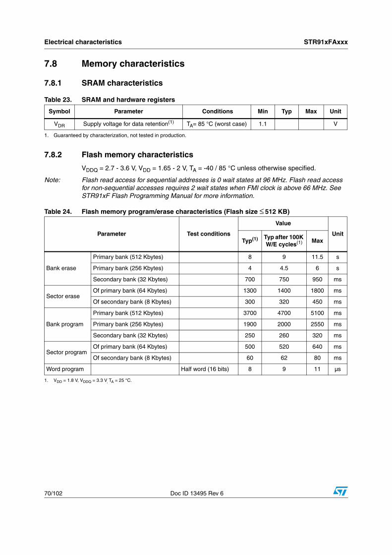
Electrical characteristics STR91xFAxxx
70/102 Doc ID 13495 Rev 6
7.8 Memory characteristics
7.8.1 SRAM characteristics
7.8.2 Flash memory characteristics
VDDQ = 2.7 - 3.6 V, VDD = 1.65 - 2 V, TA = -40 / 85 °C unless otherwise specified.
Note: Flash read access for sequential addresses is 0 wait states at 96 MHz. Flash read access for non-sequential accesses requires 2 wait states when FMI clock is above 66 MHz. See STR91xF Flash Programming Manual for more information.
Table 23. SRAM and hardware registers
Symbol Parameter Conditions Min Typ Max Unit
VDR Supply voltage for data retention(1) TA= 85 °C (worst case) 1.1 V
1. Guaranteed by characterization, not tested in production.
Table 24. Flash memory program/erase characteristics (Flash size ≤ 512 KB)
Parameter Test conditions
Value
UnitTyp(1) Typ after 100K
W/E cycles(1) Max
Bank erase
Primary bank (512 Kbytes) 8 9 11.5 s
Primary bank (256 Kbytes) 4 4.5 6 s
Secondary bank (32 Kbytes) 700 750 950 ms
Sector eraseOf primary bank (64 Kbytes) 1300 1400 1800 ms
Of secondary bank (8 Kbytes) 300 320 450 ms
Bank program
Primary bank (512 Kbytes) 3700 4700 5100 ms
Primary bank (256 Kbytes) 1900 2000 2550 ms
Secondary bank (32 Kbytes) 250 260 320 ms
Sector programOf primary bank (64 Kbytes) 500 520 640 ms
Of secondary bank (8 Kbytes) 60 62 80 ms
Word program Half word (16 bits) 8 9 11 µs
1. VDD = 1.8 V, VDDQ = 3.3 V, TA = 25 °C.

STR91xFAxxx Electrical characteristics
Doc ID 13495 Rev 6 71/102
Table 25. Flash memory program/erase characteristics (Flash size = 1 MB / 2 MB)
Parameter Test conditions
Value
UnitTyp(1) Typ after 100K
W/E cycles(1) Max
Bank erase
Primary bank (2 Mbytes) 32 36 46 s
Primary bank (1 Mbytes) 16 18 23 s
Secondary bank (128 Kbytes) 2.5 3 4 s
Sector eraseOf primary bank (64 Kbytes) 1300 1400 1800 ms
Of secondary bank (16 Kbytes) 500 600 850 ms
Bank program
Primary bank (2 Mbytes) 15 20 22 s
Primary bank (1 Mbytes) 7.5 10 11 s
Secondary bank (128 Kbytes) 1060 1140 1380 ms
Sector programOf primary bank (64 Kbytes) 500 520 640 ms
Of secondary bank (16 Kbytes) 120 130 160 ms
Word program Half word (16 bits) 8 9 11 µs
1. VDD = 1.8 V, VDDQ = 3.3 V, TA = 2 5°C.
Table 26. Flash memory endurance
Parameter Test conditionsValue
UnitMin Typ Max
Program/erase cycles Per word 100K cycles
Data retention 20 years

Electrical characteristics STR91xFAxxx
72/102 Doc ID 13495 Rev 6
7.9 EMC characteristicsSusceptibility tests are performed on a sample basis during product characterization.
7.9.1 Functional EMS (electro magnetic susceptibility)
Based on a simple running application on the product (toggling 2 LEDs through I/O ports), the product is stressed by two electro magnetic events until a failure occurs (indicated by the LEDs).
ESD: Electro-Static Discharge (positive and negative) is applied on all pins of the device until a functional disturbance occurs. This test conforms with the IEC 1000-4-2 standard.
FTB: A Burst of Fast Transient voltage (positive and negative) is applied to VDD, VDDQ and VSS through a 100pF capacitor, until a functional disturbance occurs. This test conforms with the IEC 1000-4-4 standard.
A device reset allows normal operations to be resumed. The test results are given in the table below based on the EMS levels and classes defined in application note AN1709.
Table 27. EMS data
Symbol Parameter ConditionsSeverity/Criteria(1) Unit
VFESD
Voltage limits to be applied on any I/O pin to induce a functional disturbance
VDD = 1.8 V, VDDQ = 3.3 V, TA = +25 °C, fOSC/fCPUCLK = 4 MHz/96 MHz PLL
1B
kV
VFFTB
Fast transient voltage burst limits to be applied through 100pF on VDD and VDDQ pins to induce a functional disturbance
VDD=1.8 V, VDDQ = 3.3 V, TA = +25 °C, fOSC/fCPUCLK = 4 MHz/96 MHz PLLconforms to IEC 1000-4-4
4A
1. Data based on characterization results, not tested in production.
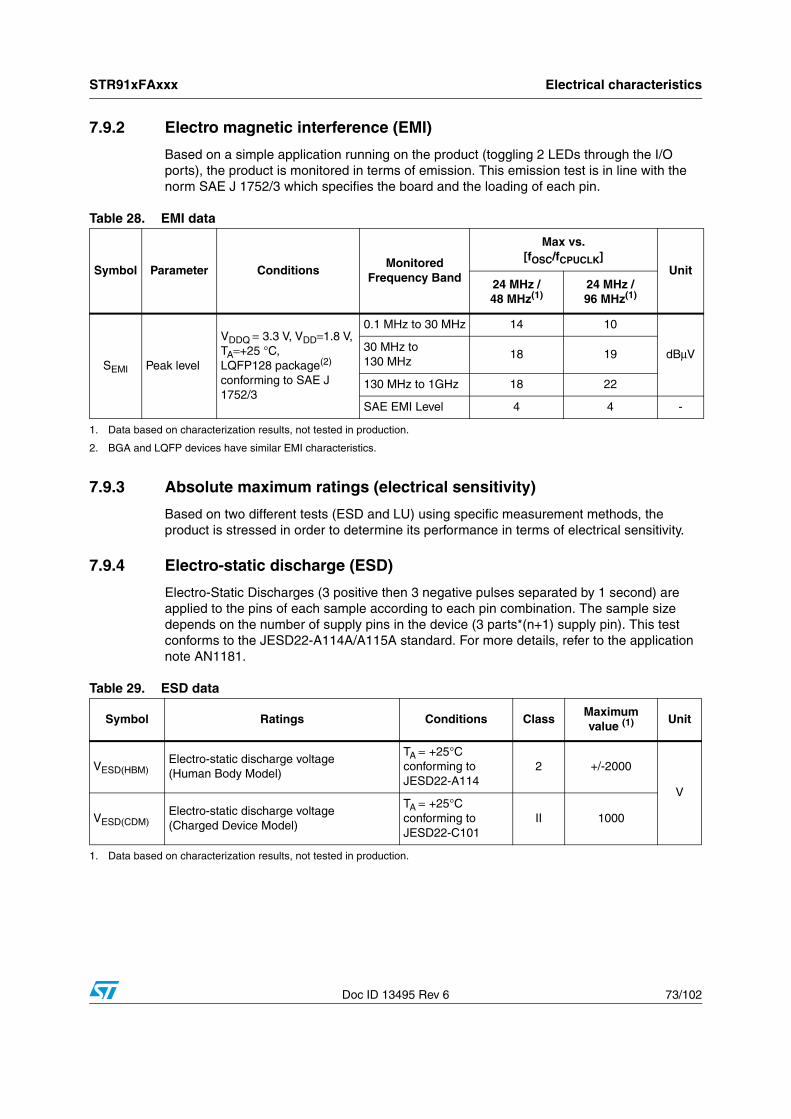
STR91xFAxxx Electrical characteristics
Doc ID 13495 Rev 6 73/102
7.9.2 Electro magnetic interference (EMI)
Based on a simple application running on the product (toggling 2 LEDs through the I/O ports), the product is monitored in terms of emission. This emission test is in line with the norm SAE J 1752/3 which specifies the board and the loading of each pin.
7.9.3 Absolute maximum ratings (electrical sensitivity)
Based on two different tests (ESD and LU) using specific measurement methods, the product is stressed in order to determine its performance in terms of electrical sensitivity.
7.9.4 Electro-static discharge (ESD)
Electro-Static Discharges (3 positive then 3 negative pulses separated by 1 second) are applied to the pins of each sample according to each pin combination. The sample size depends on the number of supply pins in the device (3 parts*(n+1) supply pin). This test conforms to the JESD22-A114A/A115A standard. For more details, refer to the application note AN1181.
Table 28. EMI data
Symbol Parameter ConditionsMonitored
Frequency Band
Max vs. [fOSC/fCPUCLK]
Unit24 MHz / 48 MHz(1)
24 MHz / 96 MHz(1)
SEMI Peak level
VDDQ = 3.3 V, VDD=1.8 V, TA=+25 °C,LQFP128 package(2)
conforming to SAE J 1752/3
0.1 MHz to 30 MHz 14 10
dBµV30 MHz to 130 MHz
18 19
130 MHz to 1GHz 18 22
SAE EMI Level 4 4 -
1. Data based on characterization results, not tested in production.
2. BGA and LQFP devices have similar EMI characteristics.
Table 29. ESD data
Symbol Ratings Conditions ClassMaximum value (1) Unit
VESD(HBM)Electro-static discharge voltage(Human Body Model)
TA = +25°C conforming to JESD22-A114
2 +/-2000
V
VESD(CDM)Electro-static discharge voltage(Charged Device Model)
TA = +25°Cconforming to JESD22-C101
II 1000
1. Data based on characterization results, not tested in production.

Electrical characteristics STR91xFAxxx
74/102 Doc ID 13495 Rev 6
7.9.5 Static latch-up
Two complementary static tests are required on 10 parts to assess the latch-up performance.
A supply overvoltage (applied to each power supply pin) and
A current injection (applied to each input, output and configurable I/O pin) are performed on each sample.
This test conforms to the EIA/JESD 78 IC latch-up standard. For more details, refer to the application note AN1181.
7.9.6 Designing hardened software to avoid noise problems
EMC characterization and optimization are performed at component level with a typical application environment and simplified MCU software. It should be noted that good EMC performance is highly dependent on the user application and the software in particular.
Therefore it is recommended that the user applies EMC software optimization and prequalification tests in relation with the EMC level requested for his application.
Software recommendations:
The software flowchart must include the management of runaway conditions such as:
Corrupted program counter
Unexpected reset
Critical Data corruption (control registers...)
Prequalification trials:
Most of the common failures (unexpected reset and program counter corruption) can be reproduced by manually forcing a low state on the RESET pin or the Oscillator pins for 1 second.
To complete these trials, ESD stress can be applied directly on the device, over the range of specification values. When unexpected behavior is detected, the software can be hardened to prevent unrecoverable errors occurring (see application note AN1015).
7.9.7 Electrical sensitivity
Table 30. Static latch-up data
Symbol Parameter Conditions Class (1)
1. Class description: A Class is an STMicroelectronics internal specification. All its limits are higher than the JEDEC specifications, that means when a device belongs to Class A it exceeds the JEDEC standard. B Class strictly covers all the JEDEC criteria (international standard).
LU Static latch-up class TA = +25 °C conforming to JESD78A II class A

STR91xFAxxx Electrical characteristics
Doc ID 13495 Rev 6 75/102
7.10 I/O characteristicsVDDQ = 2.7 - 3.6 V, VDD = 1.65 - 2 V, TA = -40 / 85 °C unless otherwise specified.
Table 31. I/O characteristics
Symbol Parameter Test conditionsValue
UnitMin Typ Max
VIH Input high level
General inputs(1) 2.0 (2) V
RESET and TCK inputs(1) 0.8 VDDQ
TAMPER_IN input(3) (Run mode)
VDDQ/2
TAMPER_IN input(3) (Standby mode)
VBAT/2
VIL Input low level
General inputs(1) 0.8
RESET and TCK inputs(1) 0.2 VDDQ
TAMPER_IN input(3) (Run mode)
VDDQ/2
TAMPER_IN input(3) (Standby mode)
VBAT/2
VHYSInput hysteresis Schmitt trigger
General inputs(4) 0 V
VOH
Output high levelHigh current pins
I/O ports 3 and 6:Push-Pull, IOH = 8mA
VDDQ-0.7
VOutput high levelStandard current pins
I/O ports 0,1,2,4,5,7,8,9:Push-Pull, IOH = 4mA
VDDQ-0.7
Output high levelJTAG JTDO pin
IOH= -100 µA VDDQ-0.1
VOL
Output low levelHigh current pins
I/O ports 3 and 6:Push-Pull, IOL = 8mA
0.4
VOutput low level
Standard current pinsI/O ports 0,1,2,4,5,7,8,9:Push-Pull, IOL = 4mA
0.4
Output low levelJTAG JTDO pin
IOL=100 µA 0.1
1. Guaranteed by characterization, not tested in production.
2. Input pins are 5V tolerant, max input voltage is 5.5V
3. Guaranteed by design, not tested in production.
4. TAMPER_IN pin and STR9 general inputs have no built-in hysteresis.

Electrical characteristics STR91xFAxxx
76/102 Doc ID 13495 Rev 6
7.11 External memory bus timingsVDDQ = 2.7 - 3.6 V, VDD = 1.65 - 2 V, TA = -40 / 85 °C, CL= 30 pF unless otherwise specified.
7.11.1 Asynchronous mode
Non Mux Write
Figure 18. Non-mux write timings
Table 32. EMI bus clock period
Symbol Parameter(1)
1. The internal EMI Bus clock signal is available externally only on LFBGA144 packages (ball M8), and not available on LQFP packages.
Value (2)
2. EMI_ratio =1/ 2 by default (can be programmed to be 1 by setting the proper bits in the SCU_CLKCNTR register)
tBCLK EMI bus clock period 1 /(fHCLK x EMI_ratio)
tWCRtWP
Address
DatatWAStWDS
EMI_CSxn
EMI_A[15:0]
EMI_D[7:0]
EMI_BWR_WRLn
Table 33. EMI non-mux write operation
Symbol ParameterValue
Min Max
tWCR WRn to CSn inactive
(tBCLK/2) - 2 ns (tBCLK/2) + 2 ns
tWAS Write address setup time
((WSTWEN + 1/2) x tBCLK ) - 2 ns ((WSTWEN + 1/2) x tBCLK) + 1 ns
tWDS Write data setup time
((WSTWEN + 1/2) x tBCLK ) - 5 ns ((WSTWEN + 1/2) x tBCLK)
tWP Write pulse width (WSTWR-WSTWEN + 1) x tBCLK - 1 ns (WSTWR-WSTWEN + 1) x tBCLK + 1.5 ns
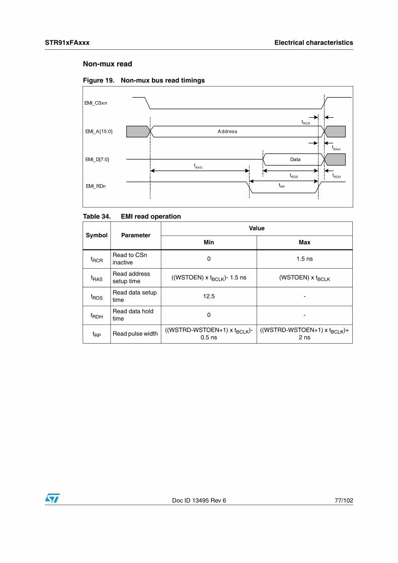
STR91xFAxxx Electrical characteristics
Doc ID 13495 Rev 6 77/102
Non-mux read
Figure 19. Non-mux bus read timings
EMI_CSxn
EMI_A[15:0] Address
DataEMI_D[7:0]
EMI_RDn
tRAS
tRP
tRDH
tRAH
tRCR
tRDS
Table 34. EMI read operation
Symbol ParameterValue
Min Max
tRCR Read to CSn inactive
0 1.5 ns
tRAS Read address setup time
((WSTOEN) x tBCLK)- 1.5 ns (WSTOEN) x tBCLK
tRDS Read data setup time
12.5 -
tRDH Read data hold time
0 -
tRP Read pulse width ((WSTRD-WSTOEN+1) x tBCLK)-
0.5 ns((WSTRD-WSTOEN+1) x tBCLK)+
2 ns

Electrical characteristics STR91xFAxxx
78/102 Doc ID 13495 Rev 6
Mux write
Figure 20. Mux write diagram
EMI_CSxn
EMI_A[23:16] Address
DataEMI_AD[15:0]
EMI_WRLnEMI_WRHn
tWAS
tWP
tWCR
tWDS
EMI_ALE
Address
tAAHtAAS
tAW
Table 35. Mux write times
Symbol ParameterValue
Min Max
tWCR WRn to CSn inactive
(tBCLK/2) - 2ns (tBCLK/2) + 2ns
tWAS Write address setup time
(WSTWEN + 1/2) x tBCLK - 2.5 ns
(WSTWEN + 1/2) xtBCLK + 2 ns
tWDSWrite data setup time
((WSTWEN - ALE_LENGTH) x tBCLK) - 2 ns
((WSTWEN - ALE_LENGTH) x tBCLK) + 1 ns
tWP Write pulse width
((WSTWR-WSTWEN + 1) x tBCLK) - 1 ns ((WSTWR-WSTWEN + 1) x tBCLK) + 1.5 ns
tAW ALE pulse width (ALE_LENGTH x tBCLK )- 3.5 ns (ALE_LENGTH x tBCLK )
tAASAddress to ALE setup time
(ALE_LENGTH x tBCLK )- 3.5 ns (ALE_LENGTH x tBCLK )
tAAHAddress to ALE hold time
(tBCLK/2) - 1 ns (tBCLK/2) + 2 ns
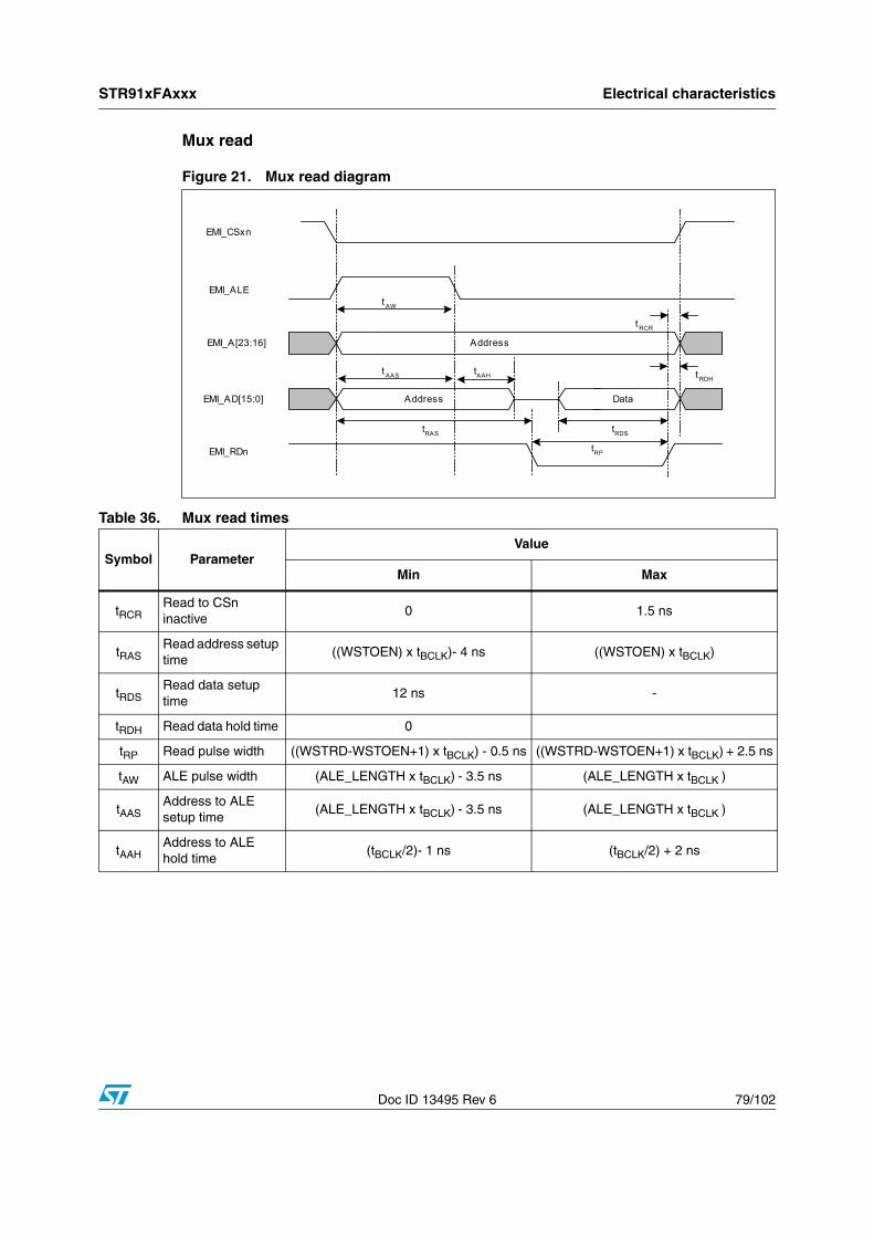
STR91xFAxxx Electrical characteristics
Doc ID 13495 Rev 6 79/102
Mux read
Figure 21. Mux read diagram
EMI_CSxn
EMI_A[23:16] Address
DataEMI_AD[15:0]
EMI_RDn
tRAS
tRP
t RDH
t RCR
tRDS
EMI_ALE
Address
tAAHt AAS
t AW
Table 36. Mux read times
Symbol ParameterValue
Min Max
tRCR Read to CSn inactive
0 1.5 ns
tRAS Read address setup time
((WSTOEN) x tBCLK)- 4 ns ((WSTOEN) x tBCLK)
tRDS Read data setup time
12 ns -
tRDH Read data hold time 0
tRP Read pulse width ((WSTRD-WSTOEN+1) x tBCLK) - 0.5 ns ((WSTRD-WSTOEN+1) x tBCLK) + 2.5 ns
tAW ALE pulse width (ALE_LENGTH x tBCLK) - 3.5 ns (ALE_LENGTH x tBCLK )
tAASAddress to ALE setup time
(ALE_LENGTH x tBCLK) - 3.5 ns (ALE_LENGTH x tBCLK )
tAAHAddress to ALE hold time
(tBCLK/2)- 1 ns (tBCLK/2) + 2 ns

Electrical characteristics STR91xFAxxx
80/102 Doc ID 13495 Rev 6
Page mode read
Figure 22. Page mode read diagram
tRCR
tADW
tRP
tRAS
tRDS tRDH
A15-A2
Addr 0 Addr 1 Addr 2 Addr 3
Data 3Data 2Data 1Data 0
CSx
EMI_RD
A15-A2
A1-A0
D0-D7
Table 37. Page mode read times
Symbol ParameterValue
Min Max
tRDH Read data hold time 0
tRDS Read data setup time 12 ns -
tADW ALE pulse width (tBCLK) - 1.5 ns (tBCLK )+ 0.5 ns
tRAS Read address setup time
((WSTOEN) x tBCLK) ((WSTOEN) x tBCLK) + 2.5 ns
tRP Read pulse width ((WSTRD-WSTOEN+1) x tBCLK) ((WSTRD-WSTOEN+1) x tBCLK) + 2 ns
tRCR Read to CSn inactive 0 1 ns

STR91xFAxxx Electrical characteristics
Doc ID 13495 Rev 6 81/102
7.11.2 Synchronous mode
Sync burst write
Figure 23. Sync burst write diagram
EMI_BCLK
EMI_ALE
CS
EMI_WE
EMI_UBEMI_LBN
EMI_BAA
EMI_WAIT
AD15:0D_OUT15:0
EMI_BCLK
EMI_ALE
EMI_WECS
EMI_BAA
A15:0
A[15:0]
D_IN[15:0]
tD1tD2
tDS tDH
DATA
tWS
EMI_WAIT
Data 0 Data 1 Data 2 Data 3 Data n
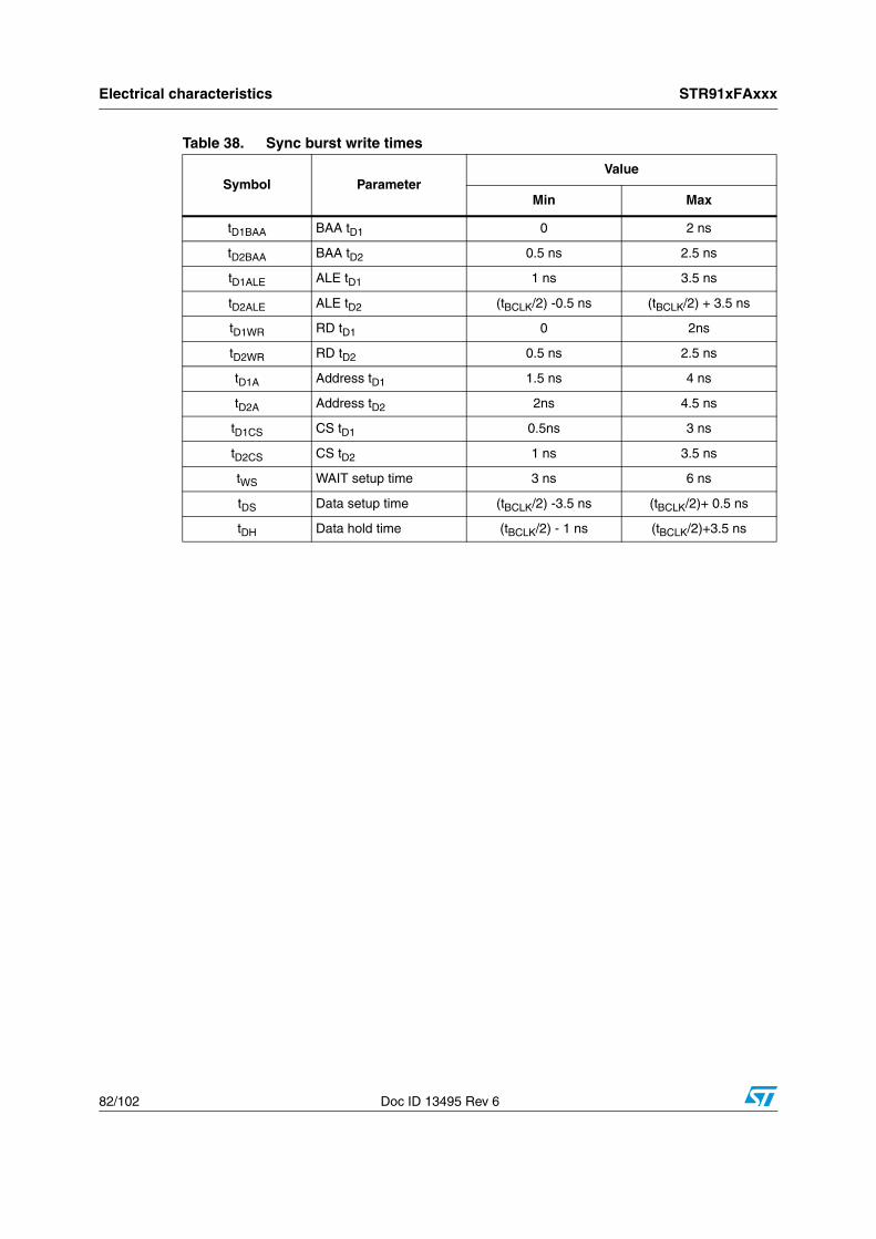
Electrical characteristics STR91xFAxxx
82/102 Doc ID 13495 Rev 6
Table 38. Sync burst write times
Symbol ParameterValue
Min Max
tD1BAA BAA tD1 0 2 ns
tD2BAA BAA tD2 0.5 ns 2.5 ns
tD1ALE ALE tD1 1 ns 3.5 ns
tD2ALE ALE tD2 (tBCLK/2) -0.5 ns (tBCLK/2) + 3.5 ns
tD1WR RD tD1 0 2ns
tD2WR RD tD2 0.5 ns 2.5 ns
tD1A Address tD1 1.5 ns 4 ns
tD2A Address tD2 2ns 4.5 ns
tD1CS CS tD1 0.5ns 3 ns
tD2CS CS tD2 1 ns 3.5 ns
tWS WAIT setup time 3 ns 6 ns
tDS Data setup time (tBCLK/2) -3.5 ns (tBCLK/2)+ 0.5 ns
tDH Data hold time (tBCLK/2) - 1 ns (tBCLK/2)+3.5 ns

STR91xFAxxx Electrical characteristics
Doc ID 13495 Rev 6 83/102
Sync burst read
Figure 24. Sync burst read diagram
D_IN[15:0]
tDS tDH
DATA
tD2tD1
tWS
EMI_WAITn
A[15:0]EMI_BAAnEMI_RDnCSxnEMI_ALE
EMI_BCLK
Table 39. Sync burst read times
Symbol ParameterValue
Min Max
tD1BAA BAA tD1 0 ns 2 ns
tD2BAA BAA tD2 0.5ns 2.5 ns
tD1ALE ALE tD1 1 ns 3.5 ns
tD2ALE ALE tD2 (tBCLK/2)+0.5 ns (tBCLK/2)+3 ns
tD1RD RD tD1 0 2 ns
tD2RD RD tD2 0.5 ns 2.5 ns
tD1A Address tD1 2 ns 4 ns
tD2A Address tD2 2.5 ns 3.5 ns
tD1CS CS tD1 0.5 ns 3 ns
tD2CS CS tD2 1 ns 3.5 ns
tWS WAIT set up time 1 ns 4 ns
tDS Data setup time 4.5 ns -
tDH Data hold time 0 -

Electrical characteristics STR91xFAxxx
84/102 Doc ID 13495 Rev 6
7.12 Communication interface electrical characteristics
7.12.1 10/100 Ethernet MAC electrical characteristics
VDDQ = 2.7 - 3.6 V, VDD = 1.65 - 2 V, TA = -40 / 85 °C unless otherwise specified.
Ethernet MII interface timings
Figure 25. MII_RX_CLK and MII_TX_CLK timing diagram
Figure 26. MDC timing diagram
Table 40. MII_RX_CLK and MII_TX_CLK timing table
Symbol Parameter SymbolValue
UnitMin Max
1 Cycle time tc(CLK) 40 ns
2 Pulse duration high tHIGH(CLK) 40% 60%
3 Pulse duration low tLOW(CLK) 40% 60%
4 Transition time tt(CLK) 1 ns
1
2
3
4 4MII_RX_TCLK, MII_TX_CLK
1
2
3
4 4
MDC
Table 41. MDC timing table
Symbol Parameter SymbolValue
UnitMin Max
1 Cycle time tc(MDC) 266 ns
2 Pulse duration high tHIGH(MDC) 40% 60%
3 Pulse duration low tLOW(MDC) 40% 60%
4 Transition time tt(MDC) 1 ns

STR91xFAxxx Electrical characteristics
Doc ID 13495 Rev 6 85/102
Ethernet MII management timings
Figure 27. Ethernet MII management timing diagram
Ethernet MII transmit timings
Figure 28. Ethernet MII transmit timing diagram
1
2 3
MDC
MDIOoutput
MDIOinput
Table 42. Ethernet MII management timing table
Symbol Parameter SymbolValue
UnitMin Max
1MDIO delay from rising edge of MDC
tc(MDIO) 2.83 ns
2MDIO setup time to rising edge of MDC
Tsu (MDIO) 2.70 ns
3MDIO hold time from rising edge of MDC
Th (MDIO) -2.03 ns
1
3
5
7
8
2
4
6
MII_TX_CLK
MII_TX_EN
MII_CRS
MII_COL
MII_TXD

Electrical characteristics STR91xFAxxx
86/102 Doc ID 13495 Rev 6
Ethernet MII receive timings
Figure 29. Ethernet MII receive timing diagram
7.12.2 USB electrical interface characteristics
USB 2.0 Compliant in Full Speed Mode
7.12.3 CAN interface electrical characteristics
Conforms to CAN 2.0B protocol specification
Table 43. Ethernet MII transmit timing table
Symbol Parameter SymbolValue
UnitMin Max
1MII_TX_CLK high to MII_TX_EN valid
tVAL(MII_TX_EN) 4.20 ns
2MII_TX_CLK high to MII_TX_EN invalid
Tinval(MII_TX_EN) 4.86 ns
3MII_CRS valid to MII_TX_CLK high
Tsu(MII_CRS) 0.61 ns
4MII_TX_CLK high to MII_CRS invalid
Th(MII_CRS) 0.00 ns
5MII_COL valid to MII_TX_CLK high
Tsu(MII_COL) 0.81 ns
6MII_TX_CLK high to MII_COL invalid
Th(MII_COL) 0.00 ns
7MII_TX_CLK high to MII_TXD valid
tVAL(MII_TXD) 5.02 ns
8MII_TXCLK high to MII_TXD invalid
Tinval(MII_TXD 5.02 ns
1 2
MII_RX_CLK
MII_RXDMII_RX_DVMII_RX_ER
Table 44. Ethernet MII receive timing table
Symbol Parameter SymbolValue
UnitMin Max
1MII_RXD valid to MII_RX_CLK high
Tsu(MII_RXD) 0.81 ns
2MII_RX_CLK high to MII_RXD invalid
Th(MII_RXD) 0.00 ns

STR91xFAxxx Electrical characteristics
Doc ID 13495 Rev 6 87/102
7.12.4 I2C electrical characteristics
VDDQ = 2.7 - 3.6 V, VDD = 1.65 - 2 V, TA = -40 / 85 °C unless otherwise specified.
Table 45. I2C electrical characteristics
Symbol ParameterStandard I2C Fast I2C
UnitMin Max Min Max
tBUFBus free time between a STOP and START condition
4.7 1.3 µs
tHD:STA
Hold time START condition. After this period, the first clock pulse is generated(1)
1. The maximum hold time of the START condition has only to be met if the interface does not stretch the low period of SCL signal
4.0 0.6 µs
tLOW Low period of the SCL clock 4.7 1.3 µs
tHIGH High period of the SCL clock 4.0 0.6 µs
tSU:STASetup time for a repeated START condition
4.7 0.6 µs
tHD:DAT Data hold time(2)
2. The device must internally provide a hold time of at least 300 ns for the SDA signal in order to bridge the undefined region of the falling edge of SCL.
0 0 ns
tSU:DAT Data setup time 250 100 ns
tRRise time of both SDA and SCL signals
100020+0.1Cb
(3)
3. Cb = total capacitance of one bus line in pF
300 ns
tFFall time of both SDA and SCL signals
30020+0.1Cb
(3) 300 ns
tSU:STO Setup time for STOP condition 4.0 0.6 µs
CbCapacitive load for each bus line
400 400 pF

Electrical characteristics STR91xFAxxx
88/102 Doc ID 13495 Rev 6
7.12.5 SPI electrical characteristics
VDDQ = 2.7 - 3.6 V, VDD = 1.65 - 2 V, TA = -40 / 85 °C unless otherwise specified.
Figure 30. SPI slave timing diagram with CPHA = 0
Table 46. SPI electrical characteristics
Symbol Parameter Test conditionsValue
UnitTyp Max
fSCLK1/tc(SCLK)
SPI clock frequencyMaster 24
MHzSlave 4
tr(SCLK)SPI clock rise and fall times 50pF load 0.1 V/ns
tf(SCLK)
tsu(SS) SS setup time Slave 1
tPCLK
th(SS) SS hold time Slave 1
tw(SCLKH)tw(SCLKL)
SCLK high and low timeMaster
Slave1
tsu(MI)tsu(SI)
Data input setup timeMasterSlave
TBD5
th(MI)th(SI)
Data input hold timeMasterSlave
TBD6
ta(SO) Data output access time Slave 6
tdis(SO) Data output disable time Slave 6
tv(SO) Data output valid time Slave (after enable edge)
6
th(SO) Data output hold time 0
tv(MO) Data output valid time Master (before capture edge)
0.25
th(MO) Data output hold time 0.25
NSS INPUT
SC
LKIN
PU
T CPHA=0
MOSI INPUT
MISO OUTPUT
CPHA=0
tc(SCLK)
tw(SCLKH)tw(SCLKL) tr(SCLK)
tf(SCLK)
tv(SO)ta(SO)
tsu(SI) th(SI)
MSB OUT
MSB IN
BIT6 OUT
LSB IN
LSB OUT
CPOL=0
CPOL=1
tsu(NSS) th(NSS)
tdis(SO)th(SO)
BIT1 IN

STR91xFAxxx Electrical characteristics
Doc ID 13495 Rev 6 89/102
Figure 31. SPI slave timing diagram with CPHA = 1
Figure 32. SPI master timing diagram
NSS INPUT
SC
LKIN
PU
T CPHA=1
MOSI INPUT
MISO OUTPUT
CPHA=1
tw(SCLKH)tw(SCLKL) tr(SCLK)
tf(SCLK)
ta(SO)
tsu(SI) th(SI)
MSB OUT BIT6 OUT LSB OUT
CPOL=0
CPOL=1
tsu(NSS) th(NSS)
tdis(SO)th(SO)
tc(SCLK)
HZ
tv(SO)
MSB IN LSB INBIT1 IN
NSS INPUT
SC
LKIO
UT
PU
T
CPHA=0
MOSI OUTPUT
MISO INPUT
CPHA=0
CPHA=1
CPHA=1
tc(SCLK)
tw(SCLKH)tw(SCLKL)
th(MI)tsu(MI)
tv(MO) th(MO)
MSB IN
MSB OUT
BIT6 IN
BIT6 OUT LSB OUT
LSB IN
CPOL=0
CPOL=1
CPOL=0
CPOL=1
tr(SCLK)tf(SCLK)

Electrical characteristics STR91xFAxxx
90/102 Doc ID 13495 Rev 6
7.13 ADC electrical characteristicsVDDQ = 2.7 - 3.6 V, VDD = 1.65 - 2 V, TA = -40 / 85 °C unless otherwise specified.
Table 47. General ADC electrical characteristics
Symbol Parameter(1) Test conditions
ValueUnit
Min Typ Max
VAIN Input voltage range 0 AVREF V
RES Resolution 10 Bits
NCH Number of input channels 8 N
fADC ADC clock frequency 25 MHz
tPOR(ADC) POR bit set to Standby mode 500 ms
tck_off(ADC) ADC clock disabled before conversion (2) 1 ms
tSTAB Stabilization time 15 µs
CIN Input capacitance 5 pF
ED Differential non-linearity (3) (4) 1 3 LSB(5)
EL Integral non-linearity (3) 3 6 LSB(5)
EO Offset error (3) 3 6 LSB(5)
EG Gain error (3) 0.5 2 LSB(5)
ET Total unadjusted error (3) 4 6 LSB(5)
IADC Power consumption 4.6 mA
IVREF Current on VREF input pin (6) (7) 920 µA
1. Guaranteed by design, not tested in production.
2. The ADC clock can be disabled by setting the ADC bit in the SCU_PCGR1 register or by setting the ACG bit in the SCU_GPIOANA register (for Rev H and higher)
3. Conditions: AVSS = 0 V, AVDD = 3.3 V fADC = 25 MHz.
4. The A/D is monotonic, there are no missing codes.
5. 1 LSB = (AVDD - AVSS)/1024
6. Data based on characterization, not tested in production.
7. Conditions: VDD=1.8 V, fCPU=96 MHz , fADC=24 MHz
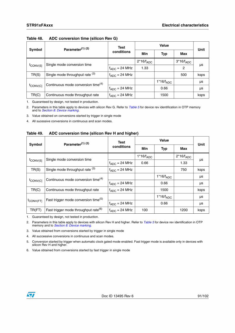
STR91xFAxxx Electrical characteristics
Doc ID 13495 Rev 6 91/102
Table 48. ADC conversion time (silicon Rev G)
Symbol Parameter(1) (2) Test conditions
ValueUnit
Min Typ Max
tCONV(S] Single mode conversion time2*16/fADC 3*16/fADC
µsfADC = 24 MHz 1.33 2
TR(S) Single mode throughput rate (3) fADC = 24 MHz 500 ksps
tCONV(C] Continuous mode conversion time(4)1*16/fADC µs
fADC = 24 MHz 0.66 µs
TR(C) Continuous mode throughput rate fADC = 24 MHz 1500 ksps
1. Guaranteed by design, not tested in production.
2. Parameters in this table apply to devices with silicon Rev G. Refer to Table 5 for device rev identification in OTP memory and to Section 8: Device marking.
3. Value obtained on conversions started by trigger in single mode
4. All sucessive conversions in continuous and scan modes.
Table 49. ADC conversion time (silicon Rev H and higher)
Symbol Parameter(1) (2) Test conditions
ValueUnit
Min Typ Max
tCONV(S] Single mode conversion time1*16/fADC 2*16/fADC
µsfADC = 24 MHz 0.66 1.33
TR(S) Single mode throughput rate (3) fADC = 24 MHz 750 ksps
tCONV(C] Continuous mode conversion time(4)1*16/fADC µs
fADC = 24 MHz 0.66 µs
TR(C) Continuous mode throughput rate fADC = 24 MHz 1500 ksps
tCONV(FT] Fast trigger mode conversion time(5)1*16/fADC µs
fADC = 24 MHz 0.66 µs
TR(FT) Fast trigger mode throughput rate(6) fADC = 24 MHz 100 1200 ksps
1. Guaranteed by design, not tested in production.
2. Parameters in this table apply to devices with silicon Rev H and higher. Refer to Table 5 for device rev identification in OTP memory and to Section 8: Device marking.
3. Value obtained from conversions started by trigger in single mode
4. All successive conversions in continuous and scan modes.
5. Conversion started by trigger when automatic clock gated mode enabled. Fast trigger mode is available only in devices with silicon Rev H and higher.
6. Value obtained from conversions started by fast trigger in single mode

Electrical characteristics STR91xFAxxx
92/102 Doc ID 13495 Rev 6
Figure 33. ADC conversion characteristics
1. Legend:(1) Example of an actual transfer curve(2) The ideal transfer curve(3) End point correlation lineET = Total Unadjusted Error: maximum deviation between the actual and the ideal transfer curves.EO = Offset Error: deviation between the first actual transition and the first ideal one.EG = Gain Error: deviation between the last ideal transition and the last actual one.ED = Differential Linearity Error: maximum deviation between actual steps and the ideal one.EL = Integral Linearity Error: maximum deviation between any actual transition and the end point correlation line.
Equation 1
EO
EG
1 LSBIDEAL
Vin (LSBIDEAL)
Digital Result 1023
1022
1021
5
4
3
2
1
0
7
6
1 2 3 4 5 6 7 1021 1022 1023 1024
(1)
(2)
ET
ED
EL
(3)
AVDDAVSS
1LSBIDEALVDDA VSSA–
1024-----------------------------------=

STR91xFAxxx Device marking
Doc ID 13495 Rev 6 93/102
8 Device marking
8.1 STR91xFAx32 / STR91xFAx42 / STR91xFAx44
Figure 34. Device marking for revision G LQFP80 and LQFP128 packages
Figure 35. Device marking for revision G LFBGA144 packages
Figure 36. Device marking for revision H LQFP80 and LQFP128 packages
Figure 37. Device marking for revision H LFBGA144 packages

Device marking STR91xFAxxx
94/102 Doc ID 13495 Rev 6
8.2 STR91xFAx46 / STR91xFAx47
Figure 38. Device marking for revision A LQFP80 and LQFP128 packages
Figure 39. Device marking for revision A LFBGA144 packages
A
A

STR91xFAxxx Package mechanical data
Doc ID 13495 Rev 6 95/102
9 Package mechanical data
Figure 40. 80-pin low profile quad flat package (LQFP80) outline
20
21
40
4160
61
80
E1 E
D1
D
1
b
e
E2
D2
PIN 1IDENTIFICATION
0.25 mmGAGE PLANE
A1
L
L1
k
A A2
A1
b
c
SEATINGPLANE
C
Cccc
Table 50. 80-pin low profile quad flat package (LQFP80) mechanical data
Dim.mm inches(1)
Min Typ Max Min Typ Max
A 1.60 0.0630
A1 0.05 0.10 0.15 0.0020 0.0039 0.0059
A2 1.35 1.40 1.45 0.0531 0.0551 0.0571
b 0.17 0.22 0.27 0.0067 0.0087 0.0106
c 0.09 0.20 0.0035 0.0079
D 13.80 14.00 14.20 0.5433 0.5512 0.5591
D1 11.90 12.00 12.10 04685 0.4724 0.4764
D2 9.50 0.3740
E 13.80 14.00 14.20 0.5433 0.5512 0.5591
E1 11.90 12.00 12.10 04685 0.4724 0.4764
E2 9.50 0.3740
e 0.50 0.0197
L 0.45 0.60 0.75 0.0177 0.0236 0.0295
L1 1.00 0.039
k 0d 7d 0d 7d
ddd 0.08 0.0031
1. Values in inches are converted from mm and rounded to 4 decimal digits.
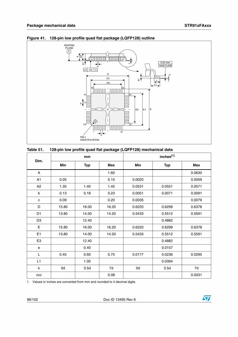
Package mechanical data STR91xFAxxx
96/102 Doc ID 13495 Rev 6
Figure 41. 128-pin low profile quad flat package (LQFP128) outline
A A2
A1
b
c32
33
64
6596
97
128
E1 E
D1
D
1
b
e
E3
D3
PIN 1IDENTIFICATION
SEATINGPLANE
C
0.25 mmGAGE PLANE
A1
L
L1
k
Cccc
Table 51. 128-pin low profile quad flat package (LQFP128) mechanical data
Dim.mm inches(1)
Min Typ Max Min Typ Max
A 1.60 0.0630
A1 0.05 0.15 0.0020 0.0059
A2 1.35 1.40 1.45 0.0531 0.0551 0.0571
b 0.13 0.18 0.23 0.0051 0.0071 0.0091
c 0.09 0.20 0.0035 0.0079
D 15.80 16.00 16.20 0.6220 0.6299 0.6378
D1 13.80 14.00 14.20 0.5433 0.5512 0.5591
D3 12.40 0.4882
E 15.80 16.00 16.20 0.6220 0.6299 0.6378
E1 13.80 14.00 14.20 0.5433 0.5512 0.5591
E3 12.40 0.4882
e 0.40 0.0157
L 0.45 0.60 0.75 0.0177 0.0236 0.0295
L1 1.00 0.0394
k 0d 3.5d 7d 0d 3.5d 7d
ccc 0.08 0.0031
1. Values in inches are converted from mm and rounded to 4 decimal digits.

STR91xFAxxx Package mechanical data
Doc ID 13495 Rev 6 97/102
Figure 42. 144-ball low profile fine pitch ball grid array package (LFBGA144) outline
Table 52. 144-ball low profile fine pitch ball grid array package (LFBGA144) mechanical data
Dim.mm inches(1)
Min Typ Max Min Typ Max
A 1.21 1.70 0.0476 0.0669
A1 0.21 0.0083
A2 1.085 0.0427
b 0.35 0.40 0.45 0.0138 0.0157 0.0177
D 9.85 10.00 10.15 0.3878 0.3937 0.3996
D1 8.80 0.3465
E 9.85 10.00 10.15 0.3878 0.3937 0.3996
E1 8.80 0.3465
e 0.80 0.0315
F 0.60 0.0236
ddd 0.10 0.0039
eee 0.15 0.0059
fff 0.08 0.0031
1. Values in inches are converted from mm and rounded to 4 decimal digits.

Package mechanical data STR91xFAxxx
98/102 Doc ID 13495 Rev 6
Figure 43. Recommended PCB design rules (0.80/0.75 mm pitch BGA)
9.1 ECOPACKTo meet environmental requirements, ST offers these devices in different grades of ECOPACK® packages, depending on their level of environmental compliance. ECOPACK® specifications, grade definitions, and product status are available at www.st.com.
9.2 Thermal characteristicsThe average chip-junction temperature, TJ must never exceed 125 °C.
The average chip-junction temperature, TJ, in degrees Celsius, may be calculated using the following equation:
TJ = TA + (PD x ΘJA) (1)
Where:
TA is the ambient temperature in ° C,
ΘJA is the package junction-to-ambient thermal resistance, in ° C/W,
PD is the sum of PINT and PI/O (PD = PINT + PI/O),
PINT is the product of IDD and VDD, expressed in Watts. This is the Chip Internal Power.
PI/O represents the power dissipation on input and output pins;
Most of the time for the applications PI/O< PINT and may be neglected. On the other hand, PI/O may be significant if the device is configured to drive continuously external modules and/or memories. The worst case PINT of the STR91xFA is 500 mW (IDD x VDD, or 250 mA x 2.0 V).
An approximate relationship between PD and TJ (if PI/O is neglected) is given by:
PD = K / (TJ + 273 °C) (2)
Therefore (solving equations 1 and 2):
K = PD x (TA + 273 °C) + ΘJA x PD2 (3)
Where:
K is a constant for the particular part, which may be determined from equation (3) by measuring PD (at equilibrium) for a known TA. Using this value of K, the values of PD and TJ may be obtained by solving equations (1) and (2) iteratively for any value of TA.
Dpad
Dsm
Dpad 0.37 mm
Dsm0.52 mm typ. (depends on solder mask registration tolerance
Solder paste 0.37 mm aperture diameter– Non solder mask defined pads are recommended
– 4 to 6 mils screen print

STR91xFAxxx Package mechanical data
Doc ID 13495 Rev 6 99/102
Table 53. Thermal characteristics
Symbol Parameter Value Unit
ΘJAThermal resistance junction-ambientLQFP 80 - 12 x 12 mm / 0.5 mm pitch
41.5 °C/W
ΘJAThermal resistance junction-ambientLQFP128 - 14 x 14 mm / 0.4 mm pitch
38 °C/W
ΘJAThermal resistance junction-ambientLFBGA 144 - 10 x 10 x 1.7 mm
36.5 °C/W

Ordering information STR91xFAxxx
100/102 Doc ID 13495 Rev 6
10 Ordering information
Table 54. Ordering information scheme
1. For a list of available options (e.g. speed, package) or for further information on any aspect of this device, please contact the ST Sales Office nearest to you.
STR9 1 2 F A W 4 4 X 6 T
Family
ARM9 microcontroller family
Series
1 = STR9 series 1
Feature set
0 = CAN, UART, IrDA, I2C, SSP
1 = USB, CAN, UART, IrDA, I2C, SSP
2 = USB, CAN, UART, IrDA, I2C, SSP, ETHERNET
Memory type
F = Flash
SRAM size
3 = 64 Kbytes4 = 96 Kbytes
Primary memory size
2 = 256 Kbytes 6= 1024 Kbytes
4 = 512 Kbytes 7= 2048 Kbytes
Package
X = plastic LQFP
H = LFBGA
Temperature range
6 = -40 to 85 °C
Shipping option
T = Tape and reel packing
Example:
No. of pins
M = 80
W = 128Z = 144
Revision at product level
A = Revison A
STR91xFAxxx Revision history
Doc ID 13495 Rev 6 101/102
11 Revision history
Table 55. Document revision history
Date Revision Changes
09-May-2007 1 Initial release
26-Nov-2007 2
Updated Standby current in Table 15: Supply current characteristics on page 64
Added Section 7.1: Parameter conditions on page 58Added Section 7.7.2: X1_CPU external clock source on page 67
Updated Section 7.11: External memory bus timings on page 76
Added Figure 14: LVD reset delay case 3 on page 63Added Table 48 and Table 49 in ADC characteristics section
Added min/max values for E, D, E1, D1 in Figure 41 on page 96
14-May-2008 3
Added 1MB and 2M devices, creating merged datasheet from seperate STR91xFAx32, 42, 44, 46 and 47 devices.
Added STR912FAW32 to Table 1: Device summary on page 1Added paragraph on voltage supply shutdown in Section 3.12 on page 24Removed DMA feature for I2C in Section 3.21 on page 33
Updated Sleep mode current in Table 10: Current characteristics on page 60
Added Table 16: Typical current consumption at 25 °C on page 65
Updated operating conditions for VDD and fCPUCLK in Section 7.3 on page 61 and Section 7.7 on page 66
Changed SPI master tSU and tH to TBD in Section Table 46. on page 88
17-Jul-2008 4
Updated Section 3.10.6 on page 22
Updated Table 11: Operating conditions on page 61
Updated ISLEEP(IDDQ) in Table 15: Supply current characteristics on page 64
Updated Table 17: Internal clock frequencies on page 66Updated Table 31: I/O characteristics on page 75
22-Dec-2008 5 Updated Section 7.7.3 on page 68. Small text changes.
02-Jul-2009 6Section 3.13.7: Tamper detection: Removed information about “Normally Closed/Tamper Open mode”.
Table 31: I/O characteristics: Updated VHYS row.

STR91xFAxxx
102/102 Doc ID 13495 Rev 6
Please Read Carefully:
Information in this document is provided solely in connection with ST products. STMicroelectronics NV and its subsidiaries (“ST”) reserve theright to make changes, corrections, modifications or improvements, to this document, and the products and services described herein at anytime, without notice.
All ST products are sold pursuant to ST’s terms and conditions of sale.
Purchasers are solely responsible for the choice, selection and use of the ST products and services described herein, and ST assumes noliability whatsoever relating to the choice, selection or use of the ST products and services described herein.
No license, express or implied, by estoppel or otherwise, to any intellectual property rights is granted under this document. If any part of thisdocument refers to any third party products or services it shall not be deemed a license grant by ST for the use of such third party productsor services, or any intellectual property contained therein or considered as a warranty covering the use in any manner whatsoever of suchthird party products or services or any intellectual property contained therein.
UNLESS OTHERWISE SET FORTH IN ST’S TERMS AND CONDITIONS OF SALE ST DISCLAIMS ANY EXPRESS OR IMPLIEDWARRANTY WITH RESPECT TO THE USE AND/OR SALE OF ST PRODUCTS INCLUDING WITHOUT LIMITATION IMPLIEDWARRANTIES OF MERCHANTABILITY, FITNESS FOR A PARTICULAR PURPOSE (AND THEIR EQUIVALENTS UNDER THE LAWSOF ANY JURISDICTION), OR INFRINGEMENT OF ANY PATENT, COPYRIGHT OR OTHER INTELLECTUAL PROPERTY RIGHT.
UNLESS EXPRESSLY APPROVED IN WRITING BY AN AUTHORIZED ST REPRESENTATIVE, ST PRODUCTS ARE NOTRECOMMENDED, AUTHORIZED OR WARRANTED FOR USE IN MILITARY, AIR CRAFT, SPACE, LIFE SAVING, OR LIFE SUSTAININGAPPLICATIONS, NOR IN PRODUCTS OR SYSTEMS WHERE FAILURE OR MALFUNCTION MAY RESULT IN PERSONAL INJURY,DEATH, OR SEVERE PROPERTY OR ENVIRONMENTAL DAMAGE. ST PRODUCTS WHICH ARE NOT SPECIFIED AS "AUTOMOTIVEGRADE" MAY ONLY BE USED IN AUTOMOTIVE APPLICATIONS AT USER’S OWN RISK.
Resale of ST products with provisions different from the statements and/or technical features set forth in this document shall immediately voidany warranty granted by ST for the ST product or service described herein and shall not create or extend in any manner whatsoever, anyliability of ST.
ST and the ST logo are trademarks or registered trademarks of ST in various countries.
Information in this document supersedes and replaces all information previously supplied.
The ST logo is a registered trademark of STMicroelectronics. All other names are the property of their respective owners.
© 2009 STMicroelectronics - All rights reserved
STMicroelectronics group of companies
Australia - Belgium - Brazil - Canada - China - Czech Republic - Finland - France - Germany - Hong Kong - India - Israel - Italy - Japan - Malaysia - Malta - Morocco - Philippines - Singapore - Spain - Sweden - Switzerland - United Kingdom - United States of America
www.st.com


![PVCPR11 Edital 3.5 GHz v03.ppt [Modo de Compatibilidade]...2011/06/09 · 35 MHz 35 MHz 10 MHz 10 MHz 10 MHz 10 MHz 10 MHz 10 MHz 3.400,00 MHz 3.600,00 MHz 10 MHz 35 MHz 10 MHz 10](https://img.dokumen.tips/doc/110x75/5f7286506e7f433bb4685297/pvcpr11-edital-35-ghz-v03ppt-modo-de-compatibilidade-20110609-35-mhz.jpg)