Embed Size (px)
Citation preview

This is a summary document. The complete document is available on the Atmel website at www.atmel.com.
ARM-based Embedded MPU
SAM9N12 SAM9CN11 SAM9CN12
SUMMARY DATASHEET
DescriptionBased on the ARM926EJ-S™ processor, the Atmel® SAM9N12/CN11/CN12 devicesoffer the frequently-requested combination of user interface functionality and high datarate connectivity, with LCD Controller, resistive touch-screen, multiple UARTs, SPI,I2C, full-speed USB Host and Device and SDIO.
The SAM9N12/CN11/CN12 support the latest generation of LPDDR/DDR2 and NANDFlash memory interfaces for program and data storage. An internal 133 MHz multi-layer bus architecture associated with eight DMA channels and distributed memory –including a 32-Kbyte SRAM – sustains the high bandwidth required by the processorand the high-speed peripherals.
The SAM9CN12/CN11 offers on-chip hardware accelerators with DMA support thatenable high-speed data encryption and authentication of transferred data or applica-tions. Supported standards are up to 256-bit AES, and FIPS Publication 180-2compliant SHA1 and SHA256. A True Random Number Generator is embedded forkey generation and exchange protocols. The devices also feature fuse bits for cryptokey (SAM9CN12), user configuration (SAM9N12 and SAM9CN11) and device configu-ration (all). The SAM9CN12 includes a secured Boot ROM; the SAM9N12 andSAM9CN11 include a standard Boot ROM.
The I/Os support 1.8V or 3.3V operation and are independently configurable forthe memory interface and peripheral I/Os. This feature eliminates the need for anyexternal level shifters, while 0.8 ball pitch packages lower PCB cost and complexity.
The SAM9N12/CN11/CN12 power management controllers feature efficient clock gat-ing and a battery backup section that minimizes power consumption in active andstandby modes. There are several devices. The table that follows presents the embed-ded features of each device.
Device SAM9N12 SAM9CN11 SAM9CN12
Standard Boot with BSC X X –
Secured Boot – – X
TRNG X X X
AES – X X
SHA – X X
11063HS–ATARM–27-Sep-13

1. Features Core
ARM926EJ-S™ ARM® Thumb® Processor running up to 400 MHz 16 Kbytes Data Cache, 16 Kbytes Instruction Cache, Memory Management Unit
Memories One 128-Kbyte internal ROM embedding standard or secure bootstrap routine. One 32-Kbyte internal SRAM, single-cycle access at system speed 32-bit External Bus Interface supporting 8-bank DDR2/LPDDR, SDR/LPSDR, Static Memories MLC/SLC NAND Controller, with up to 24-bit Programmable Multi-bit Error Correcting Code (PMECC) System running up to 133 MHz Power-on Reset, Reset Controller, Shut Down Controller, Periodic Interval Timer, Watchdog Timer and Real
Time Clock Boot Mode Select Option, Remap Command Internal Low Power 32 kHz RC and Fast 12 MHz RC Oscillators Selectable 32768 Hz Low-power Oscillator, 16 MHz Oscillator, one PLL for the system and one PLL
optimized for USB Six 32-bit-layer AHB Bus Matrix Dual Peripheral Bridge with dedicated programmable clock One dual port 8-channel DMA Controller Advanced Interrupt Controller and Debug Unit Two Programmable External Clock Signals
Low-power Mode Shut Down Controller with four 32-bit battery backup registers Clock Generator and Power Management Controller Very Slow Clock Operating Mode, Software Programmable Power Optimization Capabilities
Peripherals LCD Controller USB Device Full Speed with dedicated On-Chip Transceiver USB Host Full Speed with dedicated On-Chip Transceiver One High speed SD card and SDIO Host Controller Two Master/Slave Serial Peripheral Interfaces Two Three-channel 32-bit Timer/Counters One Synchronous Serial Controller One Four-channel 16-bit PWM Controller Two Two-wire Interfaces Four USARTs, two UARTs, one DBGU One 12-channel 10-bit Analog-to-Digital Converter with up to 5-wire resistive Touch screen support
Safety Crystal Failure Detection Independent Watchdog Power-on Reset Cells Write Protection Registers SHA (SHA1 and SHA256) Compliant with FIPS Publication 180-2, see the device configuration table in
“Description”
2SAM9N12/SAM9CN11/SAM9CN12 [SUMMARY DATASHEET]11063HS–ATARM–27-Sep-13

Cryptography TRNG True Random Number Generator compliant with NIST Special Publication 800-22 AES 256-, 192-, 128-bit Key Algorithm compliant with FIPS Publication 197 (except for SAM9N12) 256 Fuse bits for crypto key and 64 Fuse bits for device configuration, including JTAG disable and forced
boot from the on-chip ROM I/O
Four 32-bit Parallel Input/Output Controllers 105 Programmable I/O Lines Multiplexed with up to Three Peripheral I/Os Input Change Interrupt Capability on Each I/O Line, optional Schmitt Trigger input Individually Programmable Open-drain, Pull-up and Pull-down Resistor, Synchronous Output
Packages 217-ball BGA, pitch 0.8 mm 247-ball BGA, pitch 0.5 mm
3SAM9N12/SAM9CN11/SAM9CN12 [SUMMARY DATASHEET]11063HS–ATARM–27-Sep-13
2. Block Diagram
Figure 2-1. SAM9N12/CN11/CN12 Block Diagram
AIC
APB
PLLA
System Controller
PMC
PIT
WDT
OSC 32K
SHDC
RSTC
POR
DBGU
4GPBR
USART0USART1USART2USART3
SPI0
OSC16M
PIOB
POR
PIOC
RTC
RC
PIOD
SSC
PIO
PIO ARM926EJ-S
JTAG / Boundary Scan
In-Circuit Emulator
MMU
Bus Interface
I D
ICache16 Kbytes
DCache16 Kbytes
PIOA
NPCS2NPCS1SPCKM
OSIM
ISO
NPCS0
NPCS3
RTS0-
3SCK0-
3TX
D0-3
RDX0-3
ADOUL
TSADTR
IG
TSADVREFFGNDANA
VDDANA
AD1UR
AD2LL
AD3LR
AD4PI
GPAD5-
GPAD11
CTS0-
3
TDI
TDO
TMS
TCK
JTAG
SEL
RTC
K
BMS
FIQIRQ
DRXDDTXD
PCK0-PCK1
VDDBU
SHDNWKUP
XIN
NRST
XOUT
XIN32XOUT32
VDDCORE
NTRST
TC0TC1TC2TC3TC4TC5
12MRC
UTXD0-
UTXD1
URDX0-URDX1
UART0UART1SPI1 HSMCI0
SD/SDIO
FIFO
MCI0
_CK
MCI0
_DA0-
MCI0
_DA3
MCI0
_CDA
LCD
DMA
12-CH10-bit ADC
TouchScreen
PIO
PWM
PeripheralBridge
PeripheralBridge
TK TF TD RD RF RK
8-CH DMA
PWM
0-PW
M3
EBI
StaticMemory
Controller
D0-D15A0/NBS0
NCS0NCS1/SDCSNRDNWR0/NWENWR1/NBS1
SDCK, #SDCK, SDCKERAS, CASSDWE, SDA10
A1/NBS2/NWR2/DQM2
NANDOE, NANDWE
NWAIT
NCS2, NCS3, NCS4, NCS5
NANDCS
DQM[0..1]DQS[0..1]
NANDALE, NANDCLE
PIO D16-D31
NWR3/NBS3/DQM3
A20-A25
TWI0TWI1
TWCK0-
TWCK1
TWD0-
TWD1
Multi-Layer AHB Matrix
DDR2/LPDDRSDR/LPSDR
Controller
SRAM32 Kbytes
A2-A15, A19A16/BA0
A18/BA2A17/BA1
NAND FlashControllerPMECC
PMERRLOC
TCLK
0-TC
LK5
TIOA0-
TIOA5
TIOB0-
TIOB5
LCD
DAT0
-LC
DDA
T23
LCDV
SYN
C,LC
DH
SYN
C
LCD
PCK
LDD
EN,L
CD
PWM
LCD
DIS
P
AES * TRNGSHA *
USB FS OHCI
DMA
HDPHDM
USB FSDevice
DDMDDP
Transceiver
DPRAM
TransceiverFuse Box
PLLB
ROM128 Kbytes
* except SAM9N12
DMADMA
DMA DMADMA
DMA DMA DMA DMA
4SAM9N12/SAM9CN11/SAM9CN12 [SUMMARY DATASHEET]11063HS–ATARM–27-Sep-13

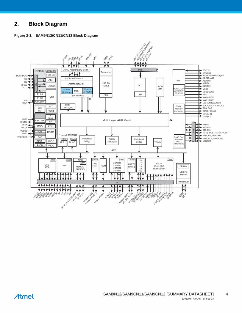
3. Signal DescriptionTable 3-1 gives details on the signal names classified by peripheral.
Table 3-1. Signal Description List
Signal Name Function Type Active Level
Clocks, Oscillators and PLLs
XIN Main Oscillator Input Input
XOUT Main Oscillator Output Output
XIN32 Slow Clock Oscillator Input Input
XOUT32 Slow Clock Oscillator Output Output
PCK0 - PCK1 Programmable Clock Output Output
Shutdown, Wakeup Logic
SHDN Shut-Down Control Output
WKUP Wake-Up Input Input
ICE and JTAG
TCK Test Clock Input
TDI Test Data In Input
TDO Test Data Out Output
TMS Test Mode Select Input
JTAGSEL JTAG Selection Input
RTCK Return Test Clock Output
Reset/Test
NRST Microcontroller Reset I/O Low
NTRST Test Reset Signal Input
BMS Boot Mode Select Input
Debug Unit - DBGU
DRXD Debug Receive Data Input
DTXD Debug Transmit Data Output
Advanced Interrupt Controller - AIC
IRQ External Interrupt Input Input
FIQ Fast Interrupt Input Input
PIO Controller - PIOA - PIOB - PIOC - PIOD
PA0 - PA31 Parallel IO Controller A I/O
PB0 - PB18 Parallel IO Controller B I/O
PC0 - PC31 Parallel IO Controller C I/O
PD0 - PD21 Parallel IO Controller D I/O
5SAM9N12/SAM9CN11/SAM9CN12 [SUMMARY DATASHEET]11063HS–ATARM–27-Sep-13
External Bus Interface - EBI
D0 -D15 Data Bus I/O
D16 -D31 Data Bus I/O
A0 - A25 Address Bus Output
NWAIT External Wait Signal Input Low
Static Memory Controller - SMC
NCS0 - NCS5 Chip Select Lines Output Low
NWR0 - NWR3 Write Signal Output Low
NRD Read Signal Output Low
NWE Write Enable Output Low
NBS0 - NBS3 Byte Mask Signal Output Low
NAND Flash Support
NFD0-NFD15 NAND Flash I/O I/O
NANDCS NAND Flash Chip Select Output Low
NANDOE NAND Flash Output Enable Output Low
NANDWE NAND Flash Write Enable Output Low
DDR2/SDRAM/LPDDR Controller
SDCK,#SDCK DDR2/SDRAM differential clock Output
SDCKE DDR2/SDRAM Clock Enable Output High
SDCS DDR2/SDRAM Controller Chip Select Output Low
BA[0..2] Bank Select Output Low
SDWE DDR2/SDRAM Write Enable Output Low
RAS - CAS Row and Column Signal Output Low
SDA10 SDRAM Address 10 Line Output
DQS[0..1] Data Strobe I/O
DQM[0..3] Write Data Mask Output
High Speed Multimedia Card Interface - HSMCI
MCI_CK Multimedia Card Clock I/O
MCI_CDA Multimedia Card Slot Command I/O
MCI_DA0 -MCI_DA7 Multimedia Card Slot Data I/O
Universal Synchronous Asynchronous Receiver Transmitter- USARTx
SCKx USARTx Serial Clock I/O
TXDx USARTx Transmit Data Output
RXDx USARTx Receive Data Input
RTSx USARTx Request To Send Output
CTSx USARTx Clear To Send Input
Table 3-1. Signal Description List (Continued)
Signal Name Function Type Active Level
6SAM9N12/SAM9CN11/SAM9CN12 [SUMMARY DATASHEET]11063HS–ATARM–27-Sep-13

Universal Asynchronous Receiver Transmitter - UARTx
UTXDx UARTx Transmit Data Output
URXDx UARTx Receive Data Input
Synchronous Serial Controller - SSC
TD SSC Transmit Data Output
RD SSC Receive Data Input
TK SSC Transmit Clock I/O
RK SSC Receive Clock I/O
TF SSC Transmit Frame Sync I/O
RF SSC Receive Frame Sync I/O
Timer Counter - TCx x=0..5
TCLKx TC Channel x External Clock Input Input
TIOAx TC Channel x I/O Line A I/O
TIOBx TC Channel x I/O Line B I/O
Serial Peripheral Interface - SPIx
SPIx_MISO Master In Slave Out I/O
SPIx_MOSI Master Out Slave In I/O
SPIx_SPCK SPI Serial Clock I/O
SPIx_NPCS0 SPI Peripheral Chip Select 0 I/O Low
SPIx_NPCS1-SPIx_NPCS3 SPI Peripheral Chip Select Output Low
Two-wire Interface -TWIx
TWDx Two-wire Serial Data I/O
TWCKx Two-wire Serial Clock I/O
Pulse Width Modulation Controller- PWM
PWM0 - PWM3 Pulse Width Modulation Output Output
USB Device Full Speed Port - UDP
DDP USB Device Data + Analog
DDM USB Device Data - Analog
USB Host Full Speed Port - UHP
HDP USB Host Data + Analog
HDM USB Host Data - Analog
LCD Controller - LCDC
LCDDAT 0-23 LCD Data Bus Output
LCDVSYNC LCD Vertical Synchronization Output
LCDHSYNC LCD Horizontal Synchronization Output
LCDPCK LCD Pixel Clock Output
Table 3-1. Signal Description List (Continued)
Signal Name Function Type Active Level
7SAM9N12/SAM9CN11/SAM9CN12 [SUMMARY DATASHEET]11063HS–ATARM–27-Sep-13

When “Reset State” is stated, the configuration is defined by the “Reset State” column of the Pin Description table.
LCDDEN LCD Data Enable Output
LCDPWM LCD Contrast Control Output
LCDDISP LCD Display Enable Output
Analog-to-Digital Converter - ADC
AD0XP_UL Top/Upper Left Channel Analog
AD1XM_UR Bottom/Upper Right Channel Analog
AD2YP_LL Right/Lower Left Channel Analog
AD3YM_SENSE Left/Sense Channel Analog
AD4LR Lower Right Channel Analog
AD5-AD11 7 Analog Inputs Analog
ADTRG ADC Trigger Input
ADVREF ADC Reference Analog
Table 3-1. Signal Description List (Continued)
Signal Name Function Type Active Level
8SAM9N12/SAM9CN11/SAM9CN12 [SUMMARY DATASHEET]11063HS–ATARM–27-Sep-13
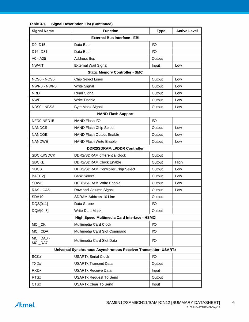
4. Package and PinoutThe SAM9CN12 is available in 217-ball and 247-ball BGA packages.
4.1 Mechanical Overview of the 217-ball BGA PackageFigure 4-1 shows the orientation of the 217-ball BGA Package
Figure 4-1. Orientation of the 217-ball BGA Package
TOP VIEW
BALL A1
12
1234567
8
91011
13
14151617
A B C D E F G H J K L M N P R T U
9SAM9N12/SAM9CN11/SAM9CN12 [SUMMARY DATASHEET]11063HS–ATARM–27-Sep-13
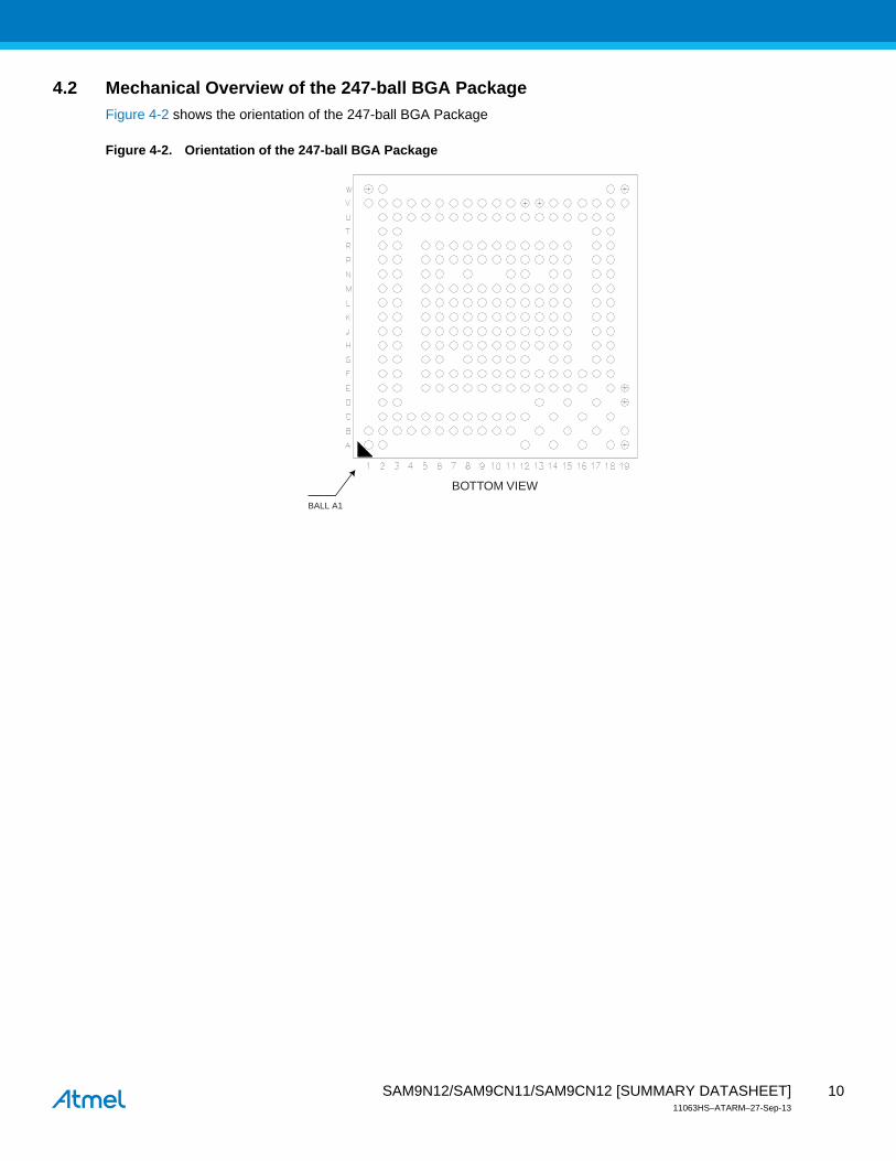
4.2 Mechanical Overview of the 247-ball BGA PackageFigure 4-2 shows the orientation of the 247-ball BGA Package
Figure 4-2. Orientation of the 247-ball BGA Package
BOTTOM VIEW
BALL A1
10SAM9N12/SAM9CN11/SAM9CN12 [SUMMARY DATASHEET]11063HS–ATARM–27-Sep-13

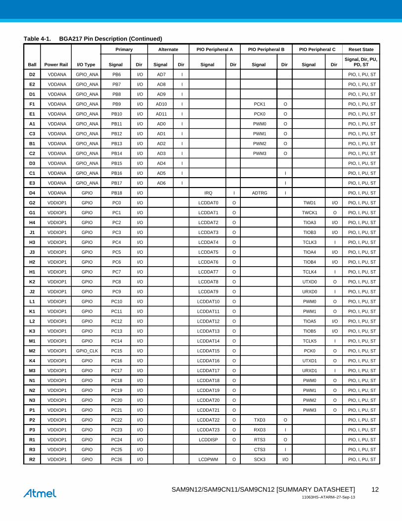
4.3 217-ball BGA Package Pinout
Table 4-1. BGA217 Pin Description
Ball Power Rail I/O Type
Primary Alternate PIO Peripheral A PIO Peripheral B PIO Peripheral C Reset State
Signal Dir Signal Dir Signal Dir Signal Dir Signal DirSignal, Dir, PU,
PD, ST
T3 VDDIOP0 GPIO PA0 I/O TXD0 O SPI1_NPCS1 O PIO, I, PU, ST
U2 VDDIOP0 GPIO PA1 I/O RXD0 I SPI0_NPCS2 O PIO, I, PU, ST
U3 VDDIOP0 GPIO PA2 I/O RTS0 O PIO, I, PU, ST
P4 VDDIOP0 GPIO PA3 I/O CTS0 I PIO, I, PU, ST
T4 VDDIOP0 GPIO PA4 I/O SCK0 I/O PIO, I, PU, ST
U4 VDDIOP0 GPIO PA5 I/O TXD1 O PIO, I, PU, ST
P5 VDDIOP0 GPIO PA6 I/O RXD1 I PIO, I, PU, ST
R4 VDDIOP0 GPIO PA7 I/O TXD2 O SPI0_NPCS1 O PIO, I, PU, ST
U6 VDDIOP0 GPIO PA8 I/O RXD2 I SPI1_NPCS0 I/O PIO, I, PU, ST
R5 VDDIOP0 GPIO PA9 I/O DRXD I PIO, I, PU, ST
R6 VDDIOP0 GPIO PA10 I/O DTXD O PIO, I, PU, ST
T5 VDDIOP0 GPIO PA11 I/O SPI0_MISO I/O MCDA4 I/O PIO, I, PU, ST
T6 VDDIOP0 GPIO PA12 I/O SPI0_MOSI I/O MCDA5 I/O PIO, I, PU, ST
U5 VDDIOP0 GPIO_CLK PA13 I/O SPI0_SPCK I/O MCDA6 I/O PIO, I, PU, ST
U7 VDDIOP0 GPIO PA14 I/O SPI0_NPCS0 I/O MCDA7 I/O PIO, I, PU, ST
T7 VDDIOP0 GPIO PA15 I/O MCDA0 I/O PIO, I, PU, ST
R7 VDDIOP0 GPIO PA16 I/O MCCDA I/O PIO, I, PU, ST
U8 VDDIOP0 GPIO_CLK PA17 I/O MCCK I/O PIO, I, PU, ST
P8 VDDIOP0 GPIO PA18 I/O MCDA1 I/O PIO, I, PU, ST
T8 VDDIOP0 GPIO PA19 I/O MCDA2 I/O PIO, I, PU, ST
R8 VDDIOP0 GPIO PA20 I/O MCDA3 I/O PIO, I, PU, ST
U9 VDDIOP0 GPIO PA21 I/O TIOA0 I/O SPI1_MISO I/O PIO, I, PU, ST
U10 VDDIOP0 GPIO PA22 I/O TIOA1 I/O SPI1_MOSI I/O PIO, I, PU, ST
T9 VDDIOP0 GPIO_CLK PA23 I/O TIOA2 I/O SPI1_SPCK I/O PIO, I, PU, ST
U11 VDDIOP0 GPIO PA24 I/O TCLK0 I TK I/O PIO, I, PU, ST
T10 VDDIOP0 GPIO PA25 I/O TCLK1 I TF I/O PIO, I, PU, ST
R9 VDDIOP0 GPIO PA26 I/O TCLK2 I TD O PIO, I, PU, ST
U12 VDDIOP0 GPIO PA27 I/O TIOB0 I/O RD I PIO, I, PU, ST
T11 VDDIOP0 GPIO PA28 I/O TIOB1 I/O RK I/O PIO, I, PU, ST
U13 VDDIOP0 GPIO PA29 I/O TIOB2 I/O RF I/O PIO, I, PU, ST
R10 VDDIOP0 GPIO PA30 I/O TWD0 I/O SPI1_NPCS3 O PIO, I, PU, ST
T12 VDDIOP0 GPIO PA31 I/O TWCK0 O SPI1_NPCS2 O PIO, I, PU, ST
E4 VDDANA GPIO PB0 I/O RTS2 O PIO, I, PU, ST
F3 VDDANA GPIO PB1 I/O CTS2 I PIO, I, PU, ST
F4 VDDANA GPIO PB2 I/O SCK2 I/O PIO, I, PU, ST
F2 VDDANA GPIO PB3 I/O SPI0_NPCS3 O PIO, I, PU, ST
G4 VDDANA GPIO_CLK PB4 I/O PIO, I, PU, ST
G3 VDDANA GPIO PB5 I/O PIO, I, PU, ST
11SAM9N12/SAM9CN11/SAM9CN12 [SUMMARY DATASHEET]11063HS–ATARM–27-Sep-13
D2 VDDANA GPIO_ANA PB6 I/O AD7 I PIO, I, PU, ST
E2 VDDANA GPIO_ANA PB7 I/O AD8 I PIO, I, PU, ST
D1 VDDANA GPIO_ANA PB8 I/O AD9 I PIO, I, PU, ST
F1 VDDANA GPIO_ANA PB9 I/O AD10 I PCK1 O PIO, I, PU, ST
E1 VDDANA GPIO_ANA PB10 I/O AD11 I PCK0 O PIO, I, PU, ST
A1 VDDANA GPIO_ANA PB11 I/O AD0 I PWM0 O PIO, I, PU, ST
C3 VDDANA GPIO_ANA PB12 I/O AD1 I PWM1 O PIO, I, PU, ST
B1 VDDANA GPIO_ANA PB13 I/O AD2 I PWM2 O PIO, I, PU, ST
C2 VDDANA GPIO_ANA PB14 I/O AD3 I PWM3 O PIO, I, PU, ST
D3 VDDANA GPIO_ANA PB15 I/O AD4 I PIO, I, PU, ST
C1 VDDANA GPIO_ANA PB16 I/O AD5 I I PIO, I, PU, ST
E3 VDDANA GPIO_ANA PB17 I/O AD6 I I PIO, I, PU, ST
D4 VDDANA GPIO PB18 I/O IRQ I ADTRG I PIO, I, PU, ST
G2 VDDIOP1 GPIO PC0 I/O LCDDAT0 O TWD1 I/O PIO, I, PU, ST
G1 VDDIOP1 GPIO PC1 I/O LCDDAT1 O TWCK1 O PIO, I, PU, ST
H4 VDDIOP1 GPIO PC2 I/O LCDDAT2 O TIOA3 I/O PIO, I, PU, ST
J1 VDDIOP1 GPIO PC3 I/O LCDDAT3 O TIOB3 I/O PIO, I, PU, ST
H3 VDDIOP1 GPIO PC4 I/O LCDDAT4 O TCLK3 I PIO, I, PU, ST
J3 VDDIOP1 GPIO PC5 I/O LCDDAT5 O TIOA4 I/O PIO, I, PU, ST
H2 VDDIOP1 GPIO PC6 I/O LCDDAT6 O TIOB4 I/O PIO, I, PU, ST
H1 VDDIOP1 GPIO PC7 I/O LCDDAT7 O TCLK4 I PIO, I, PU, ST
K2 VDDIOP1 GPIO PC8 I/O LCDDAT8 O UTXD0 O PIO, I, PU, ST
J2 VDDIOP1 GPIO PC9 I/O LCDDAT9 O URXD0 I PIO, I, PU, ST
L1 VDDIOP1 GPIO PC10 I/O LCDDAT10 O PWM0 O PIO, I, PU, ST
K1 VDDIOP1 GPIO PC11 I/O LCDDAT11 O PWM1 O PIO, I, PU, ST
L2 VDDIOP1 GPIO PC12 I/O LCDDAT12 O TIOA5 I/O PIO, I, PU, ST
K3 VDDIOP1 GPIO PC13 I/O LCDDAT13 O TIOB5 I/O PIO, I, PU, ST
M1 VDDIOP1 GPIO PC14 I/O LCDDAT14 O TCLK5 I PIO, I, PU, ST
M2 VDDIOP1 GPIO_CLK PC15 I/O LCDDAT15 O PCK0 O PIO, I, PU, ST
K4 VDDIOP1 GPIO PC16 I/O LCDDAT16 O UTXD1 O PIO, I, PU, ST
M3 VDDIOP1 GPIO PC17 I/O LCDDAT17 O URXD1 I PIO, I, PU, ST
N1 VDDIOP1 GPIO PC18 I/O LCDDAT18 O PWM0 O PIO, I, PU, ST
N2 VDDIOP1 GPIO PC19 I/O LCDDAT19 O PWM1 O PIO, I, PU, ST
N3 VDDIOP1 GPIO PC20 I/O LCDDAT20 O PWM2 O PIO, I, PU, ST
P1 VDDIOP1 GPIO PC21 I/O LCDDAT21 O PWM3 O PIO, I, PU, ST
P2 VDDIOP1 GPIO PC22 I/O LCDDAT22 O TXD3 O PIO, I, PU, ST
P3 VDDIOP1 GPIO PC23 I/O LCDDAT23 O RXD3 I PIO, I, PU, ST
R1 VDDIOP1 GPIO PC24 I/O LCDDISP O RTS3 O PIO, I, PU, ST
R3 VDDIOP1 GPIO PC25 I/O CTS3 I PIO, I, PU, ST
R2 VDDIOP1 GPIO PC26 I/O LCDPWM O SCK3 I/O PIO, I, PU, ST
Table 4-1. BGA217 Pin Description (Continued)
Ball Power Rail I/O Type
Primary Alternate PIO Peripheral A PIO Peripheral B PIO Peripheral C Reset State
Signal Dir Signal Dir Signal Dir Signal Dir Signal DirSignal, Dir, PU,
PD, ST
12SAM9N12/SAM9CN11/SAM9CN12 [SUMMARY DATASHEET]11063HS–ATARM–27-Sep-13
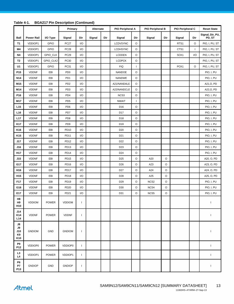
T1 VDDIOP1 GPIO PC27 I/O LCDVSYNC O RTS1 O PIO, I, PU, ST
M4 VDDIOP1 GPIO PC28 I/O LCDHSYNC O CTS1 I PIO, I, PU, ST
N4 VDDIOP1 GPIO_CLK PC29 I/O LCDDEN O SCK1 I/O PIO, I, PU, ST
T2 VDDIOP1 GPIO_CLK2 PC30 I/O LCDPCK O PIO, I, PU, ST
U1 VDDIOP1 GPIO PC31 I/O FIQ I PCK1 O PIO, I, PU, ST
P15 VDDNF EBI PD0 I/O NANDOE O PIO, I, PU
N14 VDDNF EBI PD1 I/O NANDWE O PIO, I, PU
M15 VDDNF EBI PD2 I/O A21/NANDALE O A21,O, PD
M14 VDDNF EBI PD3 I/O A22/NANDCLE O A22,O, PD
P16 VDDNF EBI PD4 I/O NCS3 O PIO, I, PU
M17 VDDNF EBI PD5 I/O NWAIT I PIO, I, PU
L15 VDDNF EBI PD6 I/O D16 O PIO, I, PU
L16 VDDNF EBI PD7 I/O D17 O PIO, I, PU
L17 VDDNF EBI PD8 I/O D18 O PIO, I, PU
K17 VDDNF EBI PD9 I/O D19 O PIO, I, PU
K16 VDDNF EBI PD10 I/O D20 O PIO, I, PU
K15 VDDNF EBI PD11 I/O D21 O PIO, I, PU
J17 VDDNF EBI PD12 I/O D22 O PIO, I, PU
J16 VDDNF EBI PD13 I/O D23 O PIO, I, PU
H17 VDDNF EBI PD14 I/O D24 O PIO, I, PU
J15 VDDNF EBI PD15 I/O D25 O A20 O A20, O, PD
G17 VDDNF EBI PD16 I/O D26 O A23 O A23, O, PD
H16 VDDNF EBI PD17 I/O D27 O A24 O A24, O, PD
H15 VDDNF EBI PD18 I/O D28 O A25 O A25, O, PD
F17 VDDNF EBI PD19 I/O D29 O NCS2 O PIO, I, PU
G16 VDDNF EBI PD20 I/O D30 O NCS4 O PIO, I, PU
E17 VDDNF EBI PD21 I/O D31 O NCS5 O PIO, I, PU
H8H9H10
VDDIOM POWER VDDIOM I I
J14K14L14
VDDNF POWER VDDNF I I
J8J9J10K9K10
GNDIOM GND GNDIOM I I
P9P12
VDDIOP0 POWER VDDIOP0 I I
L3L4
VDDIOP1 POWER VDDIOP1 I I
P6P7
P13GNDIOP GND GNDIOP I I
Table 4-1. BGA217 Pin Description (Continued)
Ball Power Rail I/O Type
Primary Alternate PIO Peripheral A PIO Peripheral B PIO Peripheral C Reset State
Signal Dir Signal Dir Signal Dir Signal Dir Signal DirSignal, Dir, PU,
PD, ST
13SAM9N12/SAM9CN11/SAM9CN12 [SUMMARY DATASHEET]11063HS–ATARM–27-Sep-13

D6 VDDBU POWER VDDBU I I
D5B3
GNDBU GND GNDBU I I
C4 VDDANA POWER VDDANA I I
B2 GNDANA GND GNDANA I I
T16 VDDPLL POWER VDDPLL I I
P14 GNDPLL GND GNDPLL I I
R14 VDDOSC POWER VDDOSC I I
R15 VDDUSB POWER VDDUSB I I
N16 VDDFUSE POWER VDDFUSE I I
M16 GNDFUSE GND GNDFUSE I
T17 GNDUSB GND GNDUSB I I
C8G15J4
P10
VDDCORE POWER VDDCORE I I
D8H14K8P11
GNDCORE GND GNDCORE I I
B14 VDDIOM EBI D0 I/O O, PD
A14 VDDIOM EBI D1 I/O O, PD
C14 VDDIOM EBI D2 I/O O, PD
D13 VDDIOM EBI D3 I/O O, PD
C13 VDDIOM EBI D4 I/O O, PD
B13 VDDIOM EBI D5 I/O O, PD
A13 VDDIOM EBI D6 I/O O, PD
C12 VDDIOM EBI D7 I/O O, PD
D12 VDDIOM EBI D8 I/O O, PD
B12 VDDIOM EBI D9 I/O O, PD
C11 VDDIOM EBI D10 I/O O, PD
D11 VDDIOM EBI D11 I/O O, PD
A12 VDDIOM EBI D12 I/O O, PD
B11 VDDIOM EBI D13 I/O O, PD
A11 VDDIOM EBI D14 I/O O, PD
C10 VDDIOM EBI D15 I/O O, PD
D17 VDDIOM EBI_O A0 O NBS0 O O, PD
C17VDDIOM EBI_O A1 O
NBS2/DQM2/NWR2
O O, PD
F16 VDDIOM EBI_O A2 O O, PD
B17 VDDIOM EBI_O A3 O O, PD
A17 VDDIOM EBI_O A4 O O, PD
F15 VDDIOM EBI_O A5 O O, PD
Table 4-1. BGA217 Pin Description (Continued)
Ball Power Rail I/O Type
Primary Alternate PIO Peripheral A PIO Peripheral B PIO Peripheral C Reset State
Signal Dir Signal Dir Signal Dir Signal Dir Signal DirSignal, Dir, PU,
PD, ST
14SAM9N12/SAM9CN11/SAM9CN12 [SUMMARY DATASHEET]11063HS–ATARM–27-Sep-13
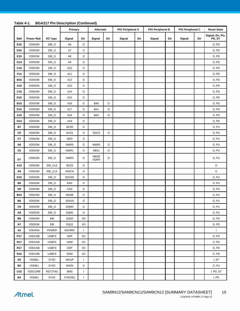
E16 VDDIOM EBI_O A6 O O, PD
D16 VDDIOM EBI_O A7 O O, PD
E15 VDDIOM EBI_O A8 O O, PD
G14 VDDIOM EBI_O A9 O O, PD
C16 VDDIOM EBI_O A10 O O, PD
F14 VDDIOM EBI_O A11 O O, PD
B16 VDDIOM EBI_O A12 O O, PD
A16 VDDIOM EBI_O A13 O O, PD
C15 VDDIOM EBI_O A14 O O, PD
D15 VDDIOM EBI_O A15 O O, PD
B15 VDDIOM EBI_O A16 O BA0 O O, PD
E14 VDDIOM EBI_O A17 O BA1 O O, PD
A15 VDDIOM EBI_O A18 O BA2 O O, PD
D14 VDDIOM EBI_O A19 O O, PD
B7 VDDIOM EBI_O NCS0 O O, PU
C5 VDDIOM EBI_O NCS1 O SDCS O O, PU
C7 VDDIOM EBI_O NRD O O, PU
A6 VDDIOM EBI_O NWR0 O NWRE O O, PU
C6 VDDIOM EBI_O NWR1 O NBS1 O O, PU
D7 VDDIOM EBI_O NWR3 O NBS3/DQM3 O O, PU
A10 VDDIOM EBI_CLK SDCK O O
A9 VDDIOM EBI_CLK #SDCK O O
D10 VDDIOM EBI_O SDCKE O O, PU
B9 VDDIOM EBI_O RAS O O, PU
D9 VDDIOM EBI_O CAS O O, PU
B10 VDDIOM EBI_O SDWE O O, PU
B6 VDDIOM EBI_O SDA10 O O, PU
C9 VDDIOM EBI_O DQM0 O O, PU
A8 VDDIOM EBI_O DQM1 O O, PU
B8 VDDIOM EBI DQS0 I/O O, PD
A7 VDDIOM EBI DQS1 I/O O, PD
A2 VDDANA POWER ADVREF I I
P17 VDDUSB USBFS HDP I/O O, PD
N17 VDDUSB USBFS HDM I/O O, PD
R17 VDDUSB USBFS DDP I/O O, PD
R16 VDDUSB USBFS DDM I/O O, PD
A5 VDDBU SYSC WKUP I I, ST
B5 VDDBU SYSC SHDN O O, PU
U15 VDDCORE RSTJTAG BMS I I, PD, ST
B4 VDDBU SYSC JTAGSEL I I, PD
Table 4-1. BGA217 Pin Description (Continued)
Ball Power Rail I/O Type
Primary Alternate PIO Peripheral A PIO Peripheral B PIO Peripheral C Reset State
Signal Dir Signal Dir Signal Dir Signal Dir Signal DirSignal, Dir, PU,
PD, ST
15SAM9N12/SAM9CN11/SAM9CN12 [SUMMARY DATASHEET]11063HS–ATARM–27-Sep-13

R12 VDDIOP0 RSTJTAG TCK I I, ST
R11 VDDIOP0 RSTJTAG TDI I I, ST
U14 VDDIOP0 RSTJTAG TDO O O
T13 VDDIOP0 RSTJTAG TMS I I, ST
T14 VDDIOP0 RSTJTAG RTCK O O
R13 VDDIOP0 RSTJTAG NRST I/O I, PU, ST
T15 VDDIOP0 RSTJTAG NTRST I I, PU, ST
A4 VDDBU CLOCK XIN32 I I
A3 VDDBU CLOCK XOUT32 O O
U17 VDDIOP0 CLOCK XIN I I
U16 VDDIOP0 CLOCK XOUT O O
N15 NC
Table 4-1. BGA217 Pin Description (Continued)
Ball Power Rail I/O Type
Primary Alternate PIO Peripheral A PIO Peripheral B PIO Peripheral C Reset State
Signal Dir Signal Dir Signal Dir Signal Dir Signal DirSignal, Dir, PU,
PD, ST
16SAM9N12/SAM9CN11/SAM9CN12 [SUMMARY DATASHEET]11063HS–ATARM–27-Sep-13

4.4 247-ball BGA Package Pinout
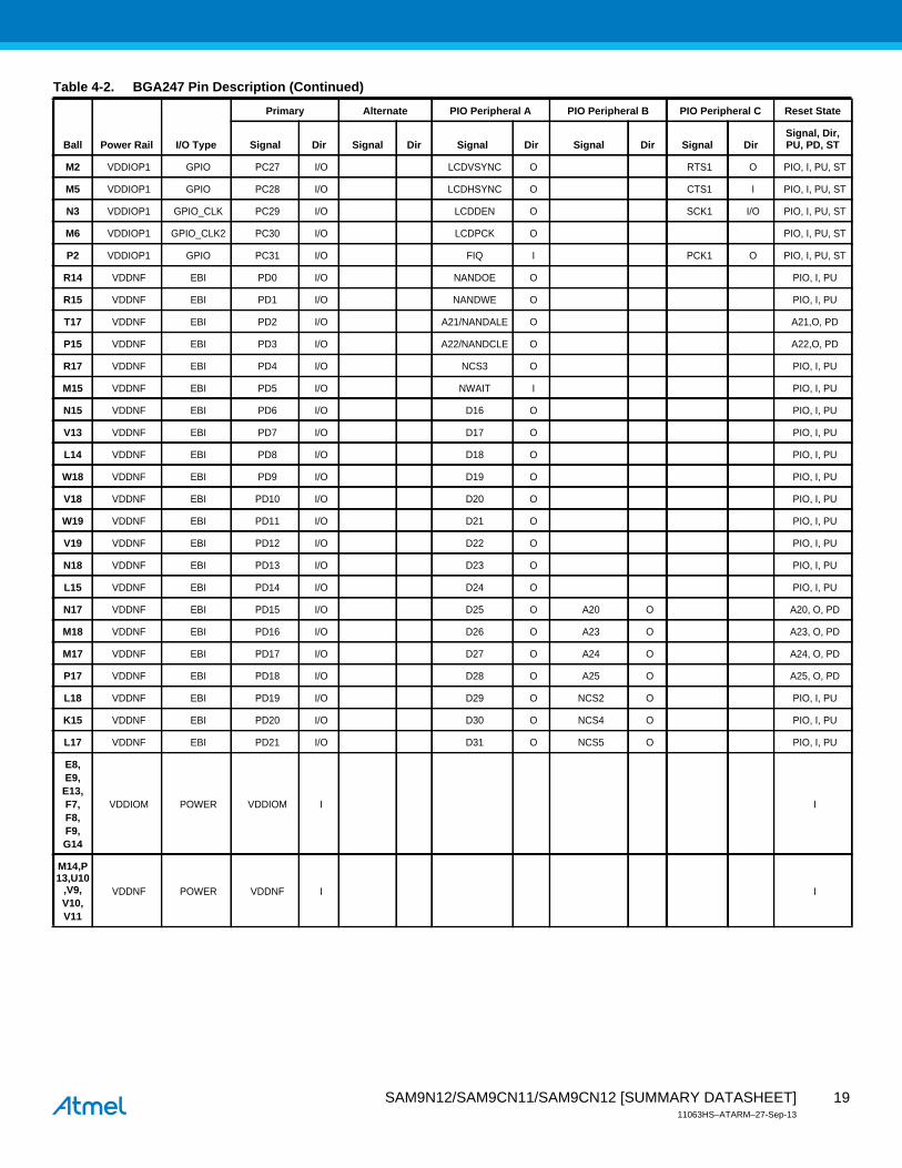
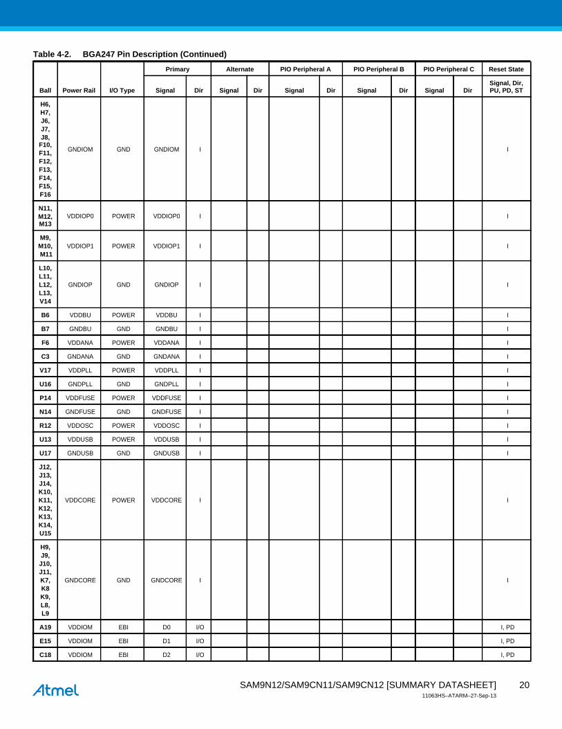
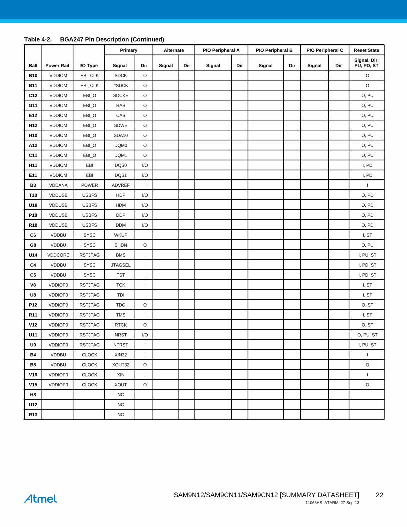
Table 4-2. BGA247 Pin Description
Ball Power Rail I/O Type
Primary Alternate PIO Peripheral A PIO Peripheral B PIO Peripheral C Reset State
Signal Dir Signal Dir Signal Dir Signal Dir Signal DirSignal, Dir, PU, PD, ST
P3 VDDIOP0 GPIO PA0 I/O TXD0 O SPI1_NPCS1 O PIO, I, PU, ST
R2 VDDIOP0 GPIO PA1 I/O RXD0 I SPI0_NPCS2 O PIO, I, PU, ST
R9 VDDIOP0 GPIO PA2 I/O RTS0 O PIO, I, PU, ST
N5 VDDIOP0 GPIO PA3 I/O CTS0 I PIO, I, PU, ST
P10 VDDIOP0 GPIO PA4 I/O SCK0 I/O PIO, I, PU, ST
R3 VDDIOP0 GPIO PA5 I/O TXD1 O PIO, I, PU, ST
R10 VDDIOP0 GPIO PA6 I/O RXD1 I PIO, I, PU, ST
T2 VDDIOP0 GPIO PA7 I/O TXD2 O SPI0_NPCS1 O PIO, I, PU, ST
P6 VDDIOP0 GPIO PA8 I/O RXD2 I SPI1_NPCS0 I/O PIO, I, PU, ST
T3 VDDIOP0 GPIO PA9 I/O DRXD I PIO, I, PU, ST
U2 VDDIOP0 GPIO PA10 I/O DTXD O PIO, I, PU, ST
P5 VDDIOP0 GPIO PA11 I/O SPI0_MISO I/O MCDA4 I/O PIO, I, PU, ST
V2 VDDIOP0 GPIO PA12 I/O SPI0_MOSI I/O MCDA5 I/O PIO, I, PU, ST
V1 VDDIOP0 GPIO_CLK PA13 I/O SPI0_SPCK I/O MCDA6 I/O PIO, I, PU, ST
W2 VDDIOP0 GPIO PA14 I/O SPI0_NPCS0 I/O MCDA7 I/O PIO, I, PU, ST
W1 VDDIOP0 GPIO PA15 I/O MCDA0 I/O PIO, I, PU, ST
V3 VDDIOP0 GPIO PA16 I/O MCCDA I/O PIO, I, PU, ST
R5 VDDIOP0 GPIO_CLK PA17 I/O MCCK I/O PIO, I, PU, ST
U3 VDDIOP0 GPIO PA18 I/O MCDA1 I/O PIO, I, PU, ST
V4 VDDIOP0 GPIO PA19 I/O MCDA2 I/O PIO, I, PU, ST
U4 VDDIOP0 GPIO PA20 I/O MCDA3 I/O PIO, I, PU, ST
V5 VDDIOP0 GPIO PA21 I/O TIOA0 I/O SPI1_MISO I/O PIO, I, PU, ST
U5 VDDIOP0 GPIO PA22 I/O TIOA1 I/O SPI1_MOSI I/O PIO, I, PU, ST
R6 VDDIOP0 GPIO_CLK PA23 I/O TIOA2 I/O SPI1_SPCK I/O PIO, I, PU, ST
R7 VDDIOP0 GPIO PA24 I/O TCLK0 I TK I/O PIO, I, PU, ST
U6 VDDIOP0 GPIO PA25 I/O TCLK1 I TF I/O PIO, I, PU, ST
V6 VDDIOP0 GPIO PA26 I/O TCLK2 I TD O PIO, I, PU, ST
R8 VDDIOP0 GPIO PA27 I/O TIOB0 I/O RD I PIO, I, PU, ST
U7 VDDIOP0 GPIO PA28 I/O TIOB1 I/O RK I/O PIO, I, PU, ST
P11 VDDIOP0 GPIO PA29 I/O TIOB2 I/O RF I/O PIO, I, PU, ST
V7 VDDIOP0 GPIO PA30 I/O TWD0 I/O SPI1_NPCS3 O PIO, I, PU, ST
N12 VDDIOP0 GPIO PA31 I/O TWCK0 O SPI1_NPCS2 O PIO, I, PU, ST
G6 VDDANA GPIO PB0 I/O RTS2 O PIO, I, PU, ST
E3 VDDANA GPIO PB1 I/O CTS2 I PIO, I, PU, ST
G5 VDDANA GPIO PB2 I/O SCK2 I/O PIO, I, PU, ST
F2 VDDANA GPIO PB3 I/O SPI0_NPCS3 O PIO, I, PU, ST
E2 VDDANA GPIO_CLK PB4 I/O PIO, I, PU, ST
E5 VDDANA GPIO PB5 I/O PIO, I, PU, ST
17SAM9N12/SAM9CN11/SAM9CN12 [SUMMARY DATASHEET]11063HS–ATARM–27-Sep-13

C2 VDDANA GPIO_ANA PB6 I/O AD7 I PIO, I, PU, ST
B2 VDDANA GPIO_ANA PB7 I/O AD8 I PIO, I, PU, ST
A2 VDDANA GPIO_ANA PB8 I/O AD9 I PIO, I, PU, ST
B1 VDDANA GPIO_ANA PB9 I/O AD10 I PCK1 O PIO, I, PU, ST
A1 VDDANA GPIO_ANA PB10 I/O AD11 I PCK0 O PIO, I, PU, ST
C7 VDDANA GPIO_ANA PB11 I/O AD0 I PWM0 O PIO, I, PU, ST
C8 VDDANA GPIO_ANA PB12 I/O AD1 I PWM1 O PIO, I, PU, ST
D3 VDDANA GPIO_ANA PB13 I/O AD2 I PWM2 O PIO, I, PU, ST
F5 VDDANA GPIO_ANA PB14 I/O AD3 I PWM3 O PIO, I, PU, ST
E6 VDDANA GPIO_ANA PB15 I/O AD4 I PIO, I, PU, ST
C9 VDDANA GPIO_ANA PB16 I/O AD5 I I PIO, I, PU, ST
D2 VDDANA GPIO_ANA PB17 I/O AD6 I I PIO, I, PU, ST
E7 VDDANA GPIO PB18 I/O IRQ I ADTRG I PIO, I, PU, ST
F3 VDDIOP1 GPIO PC0 I/O LCDDAT0 O TWD1 I/O PIO, I, PU, ST
G2 VDDIOP1 GPIO PC1 I/O LCDDAT1 O TWCK1 O PIO, I, PU, ST
L7 VDDIOP1 GPIO PC2 I/O LCDDAT2 O TIOA3 I/O PIO, I, PU, ST
G3 VDDIOP1 GPIO PC3 I/O LCDDAT3 O TIOB3 I/O PIO, I, PU, ST
H5 VDDIOP1 GPIO PC4 I/O LCDDAT4 O TCLK3 I PIO, I, PU, ST
M7 VDDIOP1 GPIO PC5 I/O LCDDAT5 O TIOA4 I/O PIO, I, PU, ST
H3 VDDIOP1 GPIO PC6 I/O LCDDAT6 O TIOB4 I/O PIO, I, PU, ST
H2 VDDIOP1 GPIO PC7 I/O LCDDAT7 O TCLK4 I PIO, I, PU, ST
J3 VDDIOP1 GPIO PC8 I/O LCDDAT8 O UTXD0 O PIO, I, PU, ST
M8 VDDIOP1 GPIO PC9 I/O LCDDAT9 O URXD0 I PIO, I, PU, ST
J5 VDDIOP1 GPIO PC10 I/O LCDDAT10 O PWM0 O PIO, I, PU, ST
K6 VDDIOP1 GPIO PC11 I/O LCDDAT11 O PWM1 O PIO, I, PU, ST
P9 VDDIOP1 GPIO PC12 I/O LCDDAT12 O TIOA5 I/O PIO, I, PU, ST
L6 VDDIOP1 GPIO PC13 I/O LCDDAT13 O TIOB5 I/O PIO, I, PU, ST
J2 VDDIOP1 GPIO PC14 I/O LCDDAT14 O TCLK5 I PIO, I, PU, ST
K3 VDDIOP1 GPIO_CLK PC15 I/O LCDDAT15 O PCK0 O PIO, I, PU, ST
K2 VDDIOP1 GPIO PC16 I/O LCDDAT16 O UTXD1 O PIO, I, PU, ST
K5 VDDIOP1 GPIO PC17 I/O LCDDAT17 O URXD1 I PIO, I, PU, ST
L3 VDDIOP1 GPIO PC18 I/O LCDDAT18 O PWM0 O PIO, I, PU, ST
N8 VDDIOP1 GPIO PC19 I/O LCDDAT19 O PWM1 O PIO, I, PU, ST
L2 VDDIOP1 GPIO PC20 I/O LCDDAT20 O PWM2 O PIO, I, PU, ST
P8 VDDIOP1 GPIO PC21 I/O LCDDAT21 O PWM3 O PIO, I, PU, ST
M3 VDDIOP1 GPIO PC22 I/O LCDDAT22 O TXD3 O PIO, I, PU, ST
L5 VDDIOP1 GPIO PC23 I/O LCDDAT23 O RXD3 I PIO, I, PU, ST
N6 VDDIOP1 GPIO PC24 I/O LCDDISP O RTS3 O PIO, I, PU, ST
N2 VDDIOP1 GPIO PC25 I/O CTS3 I PIO, I, PU, ST
P7 VDDIOP1 GPIO PC26 I/O LCDPWM O SCK3 I/O PIO, I, PU, ST
Table 4-2. BGA247 Pin Description (Continued)
Ball Power Rail I/O Type
Primary Alternate PIO Peripheral A PIO Peripheral B PIO Peripheral C Reset State
Signal Dir Signal Dir Signal Dir Signal Dir Signal DirSignal, Dir, PU, PD, ST
18SAM9N12/SAM9CN11/SAM9CN12 [SUMMARY DATASHEET]11063HS–ATARM–27-Sep-13
M2 VDDIOP1 GPIO PC27 I/O LCDVSYNC O RTS1 O PIO, I, PU, ST
M5 VDDIOP1 GPIO PC28 I/O LCDHSYNC O CTS1 I PIO, I, PU, ST
N3 VDDIOP1 GPIO_CLK PC29 I/O LCDDEN O SCK1 I/O PIO, I, PU, ST
M6 VDDIOP1 GPIO_CLK2 PC30 I/O LCDPCK O PIO, I, PU, ST
P2 VDDIOP1 GPIO PC31 I/O FIQ I PCK1 O PIO, I, PU, ST
R14 VDDNF EBI PD0 I/O NANDOE O PIO, I, PU
R15 VDDNF EBI PD1 I/O NANDWE O PIO, I, PU
T17 VDDNF EBI PD2 I/O A21/NANDALE O A21,O, PD
P15 VDDNF EBI PD3 I/O A22/NANDCLE O A22,O, PD
R17 VDDNF EBI PD4 I/O NCS3 O PIO, I, PU
M15 VDDNF EBI PD5 I/O NWAIT I PIO, I, PU
N15 VDDNF EBI PD6 I/O D16 O PIO, I, PU
V13 VDDNF EBI PD7 I/O D17 O PIO, I, PU
L14 VDDNF EBI PD8 I/O D18 O PIO, I, PU
W18 VDDNF EBI PD9 I/O D19 O PIO, I, PU
V18 VDDNF EBI PD10 I/O D20 O PIO, I, PU
W19 VDDNF EBI PD11 I/O D21 O PIO, I, PU
V19 VDDNF EBI PD12 I/O D22 O PIO, I, PU
N18 VDDNF EBI PD13 I/O D23 O PIO, I, PU
L15 VDDNF EBI PD14 I/O D24 O PIO, I, PU
N17 VDDNF EBI PD15 I/O D25 O A20 O A20, O, PD
M18 VDDNF EBI PD16 I/O D26 O A23 O A23, O, PD
M17 VDDNF EBI PD17 I/O D27 O A24 O A24, O, PD
P17 VDDNF EBI PD18 I/O D28 O A25 O A25, O, PD
L18 VDDNF EBI PD19 I/O D29 O NCS2 O PIO, I, PU
K15 VDDNF EBI PD20 I/O D30 O NCS4 O PIO, I, PU
L17 VDDNF EBI PD21 I/O D31 O NCS5 O PIO, I, PU
E8,E9,
E13,F7,F8,F9,G14
VDDIOM POWER VDDIOM I I
M14,P13,U10
,V9,V10,V11
VDDNF POWER VDDNF I I
Table 4-2. BGA247 Pin Description (Continued)
Ball Power Rail I/O Type
Primary Alternate PIO Peripheral A PIO Peripheral B PIO Peripheral C Reset State
Signal Dir Signal Dir Signal Dir Signal Dir Signal DirSignal, Dir, PU, PD, ST
19SAM9N12/SAM9CN11/SAM9CN12 [SUMMARY DATASHEET]11063HS–ATARM–27-Sep-13
H6,H7,J6,J7,J8,
F10,F11,F12,F13,F14,F15,F16
GNDIOM GND GNDIOM I I
N11,M12,M13
VDDIOP0 POWER VDDIOP0 I I
M9,M10,M11
VDDIOP1 POWER VDDIOP1 I I
L10,L11,L12,L13,V14
GNDIOP GND GNDIOP I I
B6 VDDBU POWER VDDBU I I
B7 GNDBU GND GNDBU I I
F6 VDDANA POWER VDDANA I I
C3 GNDANA GND GNDANA I I
V17 VDDPLL POWER VDDPLL I I
U16 GNDPLL GND GNDPLL I I
P14 VDDFUSE POWER VDDFUSE I I
N14 GNDFUSE GND GNDFUSE I I
R12 VDDOSC POWER VDDOSC I I
U13 VDDUSB POWER VDDUSB I I
U17 GNDUSB GND GNDUSB I I
J12,J13,J14,K10,K11,K12,K13,K14,U15
VDDCORE POWER VDDCORE I I
H9,J9,
J10,J11,K7,K8K9,L8,L9
GNDCORE GND GNDCORE I I
A19 VDDIOM EBI D0 I/O I, PD
E15 VDDIOM EBI D1 I/O I, PD
C18 VDDIOM EBI D2 I/O I, PD
Table 4-2. BGA247 Pin Description (Continued)
Ball Power Rail I/O Type
Primary Alternate PIO Peripheral A PIO Peripheral B PIO Peripheral C Reset State
Signal Dir Signal Dir Signal Dir Signal Dir Signal DirSignal, Dir, PU, PD, ST
20SAM9N12/SAM9CN11/SAM9CN12 [SUMMARY DATASHEET]11063HS–ATARM–27-Sep-13

D15 VDDIOM EBI D3 I/O I, PD
B17 VDDIOM EBI D4 I/O I, PD
E14 VDDIOM EBI D5 I/O I, PD
C16 VDDIOM EBI D6 I/O I, PD
A18 VDDIOM EBI D7 I/O I, PD
B15 VDDIOM EBI D8 I/O I, PD
G12 VDDIOM EBI D9 I/O I, PD
C14 VDDIOM EBI D10 I/O I, PD
D13 VDDIOM EBI D11 I/O I, PD
A16 VDDIOM EBI D12 I/O I, PD
A14 VDDIOM EBI D13 I/O I, PD
B13 VDDIOM EBI D14 I/O I, PD
H13 VDDIOM EBI D15 I/O I, PD
J15 VDDIOM EBI_O A0 O NBS0 O O
K18 VDDIOM EBI_O A1 ONBS2/DQM2/NWR2
O O
K17 VDDIOM EBI_O A2 O O
H15 VDDIOM EBI_O A3 O O
J18 VDDIOM EBI_O A4 O O
J17 VDDIOM EBI_O A5 O O
G17 VDDIOM EBI_O A6 O O
H17 VDDIOM EBI_O A7 O O
H18 VDDIOM EBI_O A8 O O
H14 VDDIOM EBI_O A9 O O
G18 VDDIOM EBI_O A10 O O
F18 VDDIOM EBI_O A11 O O
F17 VDDIOM EBI_O A12 O O
E19 VDDIOM EBI_O A13 O O
D19 VDDIOM EBI_O A14 O O
E18 VDDIOM EBI_O A15 O O
G15 VDDIOM EBI_O A16 O BA0 O O
E16 VDDIOM EBI_O A17 O BA1 O O
B19 VDDIOM EBI_O A18 O BA2 O O
D17 VDDIOM EBI_O A19 O O
B9 VDDIOM EBI_O NCS0 O O, PU
B8 VDDIOM EBI_O NCS1 O SDCS O O, PU
E10 VDDIOM EBI_O NRD O O, PU
G10 VDDIOM EBI_O NWR0 O NWRE O O, PU
C10 VDDIOM EBI_O NWR1 O NBS1 O O, PU
G9 VDDIOM EBI_O NWR3 O NBS3/DQM3 O O, PU
Table 4-2. BGA247 Pin Description (Continued)
Ball Power Rail I/O Type
Primary Alternate PIO Peripheral A PIO Peripheral B PIO Peripheral C Reset State
Signal Dir Signal Dir Signal Dir Signal Dir Signal DirSignal, Dir, PU, PD, ST
21SAM9N12/SAM9CN11/SAM9CN12 [SUMMARY DATASHEET]11063HS–ATARM–27-Sep-13
B10 VDDIOM EBI_CLK SDCK O O
B11 VDDIOM EBI_CLK #SDCK O O
C12 VDDIOM EBI_O SDCKE O O, PU
G11 VDDIOM EBI_O RAS O O, PU
E12 VDDIOM EBI_O CAS O O, PU
H12 VDDIOM EBI_O SDWE O O, PU
H10 VDDIOM EBI_O SDA10 O O, PU
A12 VDDIOM EBI_O DQM0 O O, PU
C11 VDDIOM EBI_O DQM1 O O, PU
H11 VDDIOM EBI DQS0 I/O I, PD
E11 VDDIOM EBI DQS1 I/O I, PD
B3 VDDANA POWER ADVREF I I
T18 VDDUSB USBFS HDP I/O O, PD
U18 VDDUSB USBFS HDM I/O O, PD
P18 VDDUSB USBFS DDP I/O O, PD
R18 VDDUSB USBFS DDM I/O O, PD
C6 VDDBU SYSC WKUP I I, ST
G8 VDDBU SYSC SHDN O O, PU
U14 VDDCORE RSTJTAG BMS I I, PU, ST
C4 VDDBU SYSC JTAGSEL I I, PD, ST
C5 VDDBU SYSC TST I I, PD, ST
V8 VDDIOP0 RSTJTAG TCK I I, ST
U8 VDDIOP0 RSTJTAG TDI I I, ST
P12 VDDIOP0 RSTJTAG TDO O O, ST
R11 VDDIOP0 RSTJTAG TMS I I, ST
V12 VDDIOP0 RSTJTAG RTCK O O, ST
U11 VDDIOP0 RSTJTAG NRST I/O O, PU, ST
U9 VDDIOP0 RSTJTAG NTRST I I, PU, ST
B4 VDDBU CLOCK XIN32 I I
B5 VDDBU CLOCK XOUT32 O O
V16 VDDIOP0 CLOCK XIN I I
V15 VDDIOP0 CLOCK XOUT O O
H8 NC
U12 NC
R13 NC
Table 4-2. BGA247 Pin Description (Continued)
Ball Power Rail I/O Type
Primary Alternate PIO Peripheral A PIO Peripheral B PIO Peripheral C Reset State
Signal Dir Signal Dir Signal Dir Signal Dir Signal DirSignal, Dir, PU, PD, ST
22SAM9N12/SAM9CN11/SAM9CN12 [SUMMARY DATASHEET]11063HS–ATARM–27-Sep-13
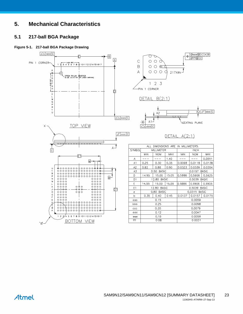
5. Mechanical Characteristics
5.1 217-ball BGA Package
Figure 5-1. 217-ball BGA Package Drawing
23SAM9N12/SAM9CN11/SAM9CN12 [SUMMARY DATASHEET]11063HS–ATARM–27-Sep-13

5.2 247-ball BGA Package
Figure 5-2. 247-ball BGA Package Drawing
24SAM9N12/SAM9CN11/SAM9CN12 [SUMMARY DATASHEET]11063HS–ATARM–27-Sep-13
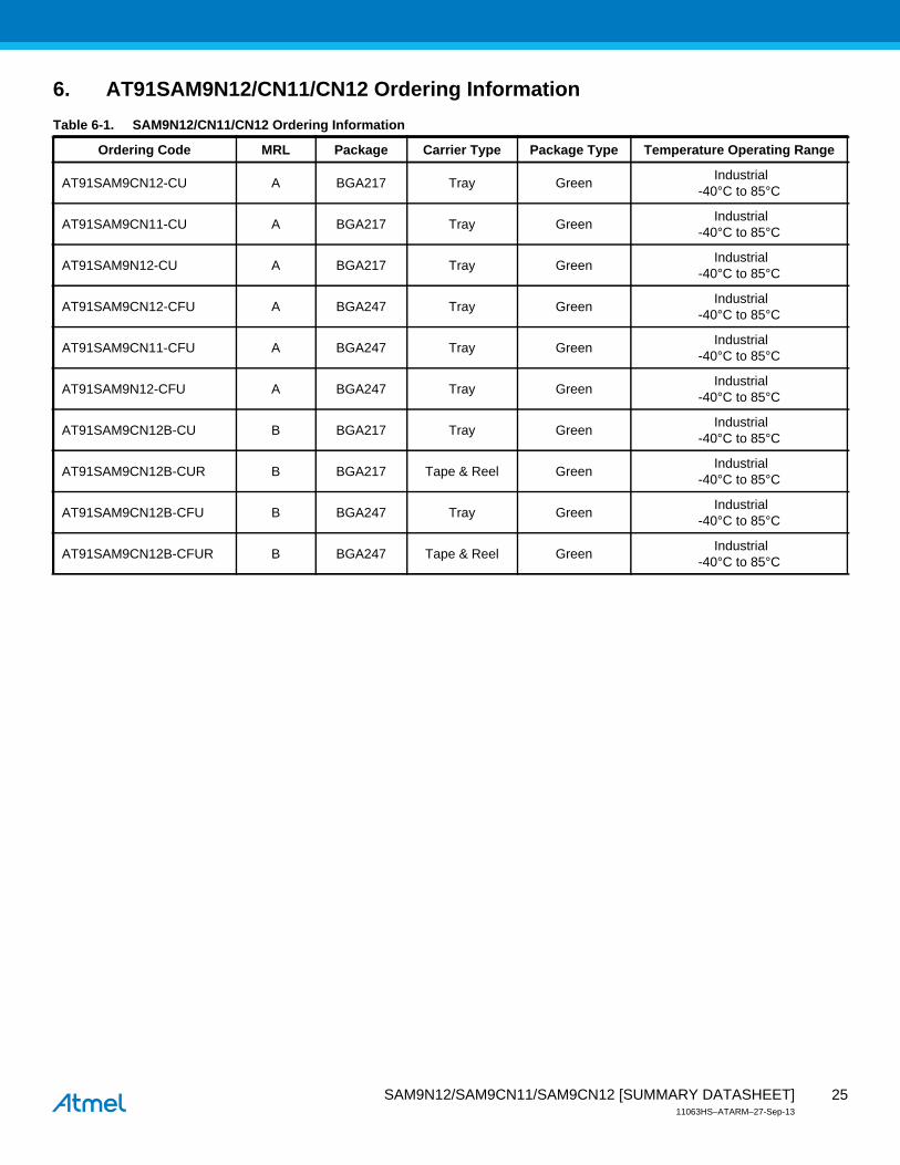
6. AT91SAM9N12/CN11/CN12 Ordering InformationTable 6-1. SAM9N12/CN11/CN12 Ordering Information
Ordering Code MRL Package Carrier Type Package Type Temperature Operating Range
AT91SAM9CN12-CU A BGA217 Tray Green Industrial-40°C to 85°C
AT91SAM9CN11-CU A BGA217 Tray Green Industrial-40°C to 85°C
AT91SAM9N12-CU A BGA217 Tray Green Industrial-40°C to 85°C
AT91SAM9CN12-CFU A BGA247 Tray Green Industrial-40°C to 85°C
AT91SAM9CN11-CFU A BGA247 Tray Green Industrial-40°C to 85°C
AT91SAM9N12-CFU A BGA247 Tray Green Industrial-40°C to 85°C
AT91SAM9CN12B-CU B BGA217 Tray Green Industrial-40°C to 85°C
AT91SAM9CN12B-CUR B BGA217 Tape & Reel Green Industrial-40°C to 85°C
AT91SAM9CN12B-CFU B BGA247 Tray Green Industrial-40°C to 85°C
AT91SAM9CN12B-CFUR B BGA247 Tape & Reel Green Industrial-40°C to 85°C
25SAM9N12/SAM9CN11/SAM9CN12 [SUMMARY DATASHEET]11063HS–ATARM–27-Sep-13

Revision History
In the table that follows, the most recent version of the document appears first.
“rfo” indicates changes requested during the document review and approval loop.
Doc. Rev Comments Change Request Ref.
11063HS
“Description”, revised content and presentation.
Section 1. “Features”:
- added a list on safety features
- moved SHA references to “Safety” list
Section 3. “Signal Description”:
- removed references to VBG pins in Table 3-1, “Signal Description List”
- removed Table 3-2 SAM9N12/CN11/CN12 I/O Type Description
Table 6-1, “SAM9N12/CN11/CN12 Ordering Information”:
- added MRL and Carrier Type columns
- added ordering codes for MRLB
rfo
rfo
8531/rfo
rfo
11063GS
Table 6-1, “SAM9N12/CN11/CN12 Ordering Information” updated with new ordering codes for BGA247 packages.
Section “Description” put before Section 1. “Features”.
Sections 5 to 9 deleted (5 Power Considerations, 6 Memories, 7 System Controller, 8 Peripherals, 9 Embedded Peripherals).
8804
rfo
11063FS
Added “Write Protected Registers in Section 1. “Features”.
Product name updated to SAM9N12/SAM9CN11/SAM9CN12.
Section “Description” updated with the various devices configurations: device configuration table added.
Bullets for SAM9CN11 and SAM9N12 added in Section 7.3 “Chip Identification”.
Ordering codes added for SAM9N12 and SAM9CN11 in Table 6-1, “SAM9N12/CN11/CN12 Ordering Information”.
8213
8244
11063ES
Section 1. “Features”, Memories, “Boot on NANDFlash, SDCard, DataFlash or serial DataFlash. Programmable order” removed.
Section “Description”, 125 MHz --> 133 MHz
“FIPS PUB 46-3 compliant TDES” removed from 3rd paragraph
Table 3-1, “Signal Description List”, NFD0-NFD16 --> NFD0-NFD15
Section 7.3 “Chip Identification”, Chip ID: 0x819A_05A0 --> 0x819A_05A1
Table 8-1, “SAM9N12/CN11/CN12 Peripheral Identifiers”, Replaced keyword ‘Reserved’ on 4th row with ‘FUSE’
Section 9.8 “Power Management Controller (PMC)”, 250MHz DDR --> 133 MHz DDR
rfo
7928
rfo
rfo
rfo
8039
7975
11063DS
Section 1. “Features”,
Updated...”Processor running up to 400 MHz...”
Updated...”System running up to 133 MHz...”
Back page:
Updated point of contact information.
7847
Marcom
26SAM9N12/SAM9CN11/SAM9CN12 [SUMMARY DATASHEET]11063HS–ATARM–27-Sep-13

11063CS
Section 1. “Features”SLC NAND Flash is supported.
Section “Description”, 1st paragraph, the 2nd sentence was removed.
Table 4-1, “BGA217 Pin Description”, table updated with values in Ball column.
Table 5-1, “SAM9N12/CN11/CN12 Power Supplies”, VDDFUSE Voltage Range updated, 3.0V-3.6V.
Section 6.3.3 “DDR-SDRAM Controller”, revised.
Section 7.3 “Chip Identification”, removed “two” lines.
Section 8.4 “Peripheral Signal Multiplexing on I/O Lines”, removed irrelevant text.
Elsewhere, minor grammar revisions. Advance Information status removed.
rfo
7395
rfo
7269
7392
rfo
11063BS Table 4-2, “BGA247 Pin Description”, updated. 7271
11063AS First issue
Doc. Rev Comments Change Request Ref.
27SAM9N12/SAM9CN11/SAM9CN12 [SUMMARY DATASHEET]11063HS–ATARM–27-Sep-13
Atmel Corporation1600 Technology DriveSan Jose, CA 95110USATel: (+1) (408) 441-0311Fax: (+1) (408) 487-2600www.atmel.com
Atmel Asia LimitedUnit 01-5 & 16, 19FBEA Tower, Millennium City 5418 Kwun Tong RoadKwun Tong, KowloonHONG KONGTel: (+852) 2245-6100Fax: (+852) 2722-1369
Atmel Munich GmbHBusiness CampusParkring 4D-85748 Garching b. MunichGERMANYTel: (+49) 89-31970-0Fax: (+49) 89-3194621
Atmel Japan G.K.16F Shin-Osaki Kangyo Bldg1-6-4 Osaki, Shinagawa-kuTokyo 141-0032JAPANTel: (+81) (3) 6417-0300Fax: (+81) (3) 6417-0370
© 2013 Atmel Corporation. All rights reserved. / Rev.: 11063HS–ATARM–27-Sep-13
Atmel®, Atmel logo and combinations thereof, Enabling Unlimited Possibilities®, SAM-BA® and others are registered trademarks or trademarks of Atmel Corporation or its subsidiaries. ARM®, ARM926EJ-S™, Thumb®, AMBA™ and others are the registered trademarks or trademarks of ARM Ltd. Other terms and product names may be trademarks of others.
Disclaimer: The information in this document is provided in connection with Atmel products. No license, express or implied, by estoppel or otherwise, to any intellectual property right is granted by this document or in connection with the sale of Atmel products. EXCEPT AS SET FORTH IN THE ATMEL TERMS AND CONDITIONS OF SALES LOCATED ON THE ATMEL WEBSITE, ATMEL ASSUMES NO LIABILITY WHATSOEVER AND DISCLAIMS ANY EXPRESS, IMPLIED OR STATUTORY WARRANTY RELATING TO ITS PRODUCTS INCLUDING, BUT NOT LIMITED TO, THE IMPLIED WARRANTY OF MERCHANTABILITY, FITNESS FOR A PARTICULAR PURPOSE, OR NON-INFRINGEMENT. IN NO EVENT SHALL ATMEL BE LIABLE FOR ANY DIRECT, INDIRECT, CONSEQUENTIAL, PUNITIVE, SPECIAL OR INCIDENTAL DAMAGES (INCLUDING, WITHOUT LIMITATION, DAMAGES FOR LOSS AND PROFITS, BUSINESS INTERRUPTION, OR LOSS OF INFORMATION) ARISING OUT OF THE USE OR INABILITY TO USE THIS DOCUMENT, EVEN IF ATMEL HAS BEEN ADVISED OF THE POSSIBILITY OF SUCH DAMAGES. Atmel makes no representations or warranties with respect to the accuracy or completeness of the contents of this document and reserves the right to make changes to specifications and products descriptions at any time without notice. Atmel does not make any commitment to update the information contained herein. Unless specifically provided otherwise, Atmel products are not suitable for, and shall not be used in, automotive applications. Atmel products are not intended, authorized, or warranted for use as components in applications intended to support or sustain life.


![M1A2 Embedded Training [Read-Only] · M1A2 SEP Tank Embedded Training System Architecture GCDP FCEU GPS CITV EU CEU DECU POSNAV DID MPU Gunner’s CDU CCHA Handles Turned Off For](https://img.dokumen.tips/doc/110x75/5ec9acb55f0730394d28d1ad/m1a2-embedded-training-read-only-m1a2-sep-tank-embedded-training-system-architecture.jpg)