Embed Size (px)
Citation preview

HAL Id: ujm-00289036https://hal-ujm.archives-ouvertes.fr/ujm-00289036
Submitted on 19 Jun 2008
HAL is a multi-disciplinary open accessarchive for the deposit and dissemination of sci-entific research documents, whether they are pub-lished or not. The documents may come fromteaching and research institutions in France orabroad, or from public or private research centers.
L’archive ouverte pluridisciplinaire HAL, estdestinée au dépôt et à la diffusion de documentsscientifiques de niveau recherche, publiés ou non,émanant des établissements d’enseignement et derecherche français ou étrangers, des laboratoirespublics ou privés.
Area–time efficient hardware architecture for factoringintegers with the elliptic curve method
Jan Pelzl, Martin Simka, Thorsten Kleinjung, Milos Drutarovsky, ViktorFischer, Christof Paar
To cite this version:Jan Pelzl, Martin Simka, Thorsten Kleinjung, Milos Drutarovsky, Viktor Fischer, et al.. Area–timeefficient hardware architecture for factoring integers with the elliptic curve method. InformationSecurity, IEE Proceedings, 2005, 152 (1), pp.67-78. �ujm-00289036�

Area-Time Efficient Hardware Architecture
for Factoring Integers with the Elliptic Curve Method
Jan Pelzl1, Martin Simka2, Thorsten Kleinjung3,
Milos Drutarovsky2, Viktor Fischer4, Christof Paar1
1 Horst Gortz Institute for IT Security, Ruhr University Bochum, Germany
{pelzl,cpaar}@crypto.rub.de
2 Department of Electronics and Multimedia Communications, Technical University of Kosice,
Park Komenskeho 13, 04120 Kosice, Slovak Republic
{Martin.Simka,Milos.Drutarovsky}@tuke.sk
3 University of Bonn, Department of Mathematics, Beringstraße 1, D-53115 Bonn, Germany
4 Laboratoire Traitement du Signal et Instrumentation, Unite Mixte de Recherche CNRS 5516,
Universite Jean Monnet, 10, rue Barrouin, 42000 Saint-Etienne, France
Abstract
Since the introduction of public key cryptography, the problem of factoring large composites
is of increased interest. The security of the most popular asymmetric cryptographic scheme
RSA depends on the hardness of factoring large numbers. The best known method for factoring
large integers is the General Number Field Sieve (GNFS). One important step within the
GNFS is the factorization of mid-size numbers for smoothness testing, an efficient algorithm
for which is the Elliptic Curve Method (ECM). Since the smoothness testing is also suitable for
parallelization, it is promising to improve ECM via special-purpose hardware. We show that
massive parallel and cost efficient ECM hardware engines can improve the cost-time product
of the RSA moduli factorization via the GNFS considerably.
1

The computation of ECM is a classical example for an algorithm that can be significantly
accelerated through special-purpose hardware. In this work, we thoroughly analyze the prereq-
uisites for an area-time efficient hardware architecture for ECM. We present an implementation
of ECM to factor numbers up to 200 bits, which is also scalable to other bit lengths. ECM
is realized as a software-hardware co-design on an FPGA and an embedded microcontroller
(system-on-chip). Furthermore, we provide estimates for state-of-the-art CMOS implementa-
tion of the design and for the application of massive parallel ECM engines to the GNFS. This
appears to be the first publication of a realized hardware implementation of ECM, and the
first description of GNFS acceleration through hardware-based ECM.
Keywords: factorization, elliptic curve method, system-on-chip, field programmable gate ar-
ray.
1 Introduction
Since the ancient world, factoring integers has been investigated painstakingly by many mathe-
maticians. With the dawn of asymmetric cryptography in the mid 1970s the problem of factoring
large composites has again evoked increased mathematical interest. These days, the by far most
popular asymmetric cryptosystem is RSA which was developed by Ronald Rivest, Adi Shamir and
Leonard Adleman in 1977 [1]. The security of the RSA cryptosystem relies on the difficulty of
factoring large numbers. Hence, the development of a fast factorization method could allow for
cryptanalysis of RSA messages and signatures. However, till now the problem of factorization has
remained hard.
Several efficient algorithms for factoring integers have been proposed. Each algorithm is appro-
priate for a different situation. For instance, the Elliptic Curve Method (ECM, see [2]) allows for
efficient factoring of medium sized numbers with relatively small factors. The Generalized Number
Field Sieve (GNFS, see [3]) is best for factoring numbers with large factors and, hence, can be
used for attacking the RSA cryptosystem. However, as an intermediate step, the GNFS requires
a method to efficiently factor lots of smaller numbers (factorization of the rests). An appropriate
choice for this task is MPQS (Multiple Polynomial Quadratic Sieve) or ECM.
The current world record in factoring a random RSA modulus is 576 bits and was achieved
with a complete software implementation of the GNFS in 2003 [4], using MPQS for the factoriza-
2

tion of the rests. For larger moduli it will become crucial to use special hardware for factoring.
Recently, some new hardware architectures for the sieving step in GNFS have been proposed
(e.g., SHARK [5], TWIRL [6]). The efficiency of, e.g., SHARK (and possibly other innovative
GNFS realizations) is directly related to efficient support units for smoothness testing within the
architecture.
It appears that the use of ECM rather than MPQS is the better choice for this task, since
the MPQS requires a larger silicon area and irregular operations. On the other hand, ECM is an
almost ideal algorithm for dramatically improving the time-cost product through special purpose
hardware. First, it performs a very high number of operations on a very small set of input data, and
is, thus, not very I/O intensive. Second, it requires relatively little memory. Third, the operands
needed for supporting GNFS are well beyond the width of current computer buses, arithmetic
units, and registers, so that special purpose hardware can provide a much better fit. Lastly, it
should be noted that the nature of the smoothness testing in the GNFS allows for a very high
degree of parallelization. Hence, the key for efficient ECM hardware lies in fast arithmetic units.
Such units for modular addition and multiplication have been studied thoroughly in the last few
years, e.g., for the use in cryptographic devices using ECC (Elliptic Curve Cryptography), see,
e.g., [7, 8]. Therefore, we could exploit the well developed area of ECC architectures for our ECM
design.
In this work, we present an efficient hardware implementation of ECM to factor numbers up
to approximately 200 bits, which is also scalable to other bit lengths. We provide an elaborate
specification of an area-time (AT) efficient ECM architecture, especially suited for hardware imple-
mentations. For proof-of-concept purpose, the ECM architecture has been realized as a software-
hardware co-design on an FPGA and an embedded microcontroller (system-on-chip). Timings of
the real hardware for the operations of the ECM algorithm are presented. We also provide esti-
mates for a state-of-the-art CMOS implementation of the design and for the application of massive
parallel ECM engines to the GNFS. Our design has a good scalability to larger and smaller bit
lengths. In some range, both the time and the silicon area depend linearly on the bit length. Such
a design perfectly fits the needs of more recent proposals for hardware architectures for the GNFS
(see, e.g., [5]) and can reduce the overall costs of a GNFS device considerably.
There are many possible improvements of the original ECM. Based on these improvements,
3

we adapted the method to the very restrictive memory requirements of efficient hardware, thus,
minimizing the AT product. The parameters used in our implementation are best suited to find
factors of up to about 40 bits.
For the implementation, a highly efficient modular multiplication architecture described by
Tenca and Koc (see [9]) is used and allows for reliable estimates for a future ASIC implementation.
We propose to group about 1000 ECM units together on an ASIC and describe a controlling unit
that synchronously feeds the units with programming steps, such that the ECM algorithm does
not need to be stored in every single unit. In this way we keep the overall ASIC area small and
still do not need much bandwidth for communication.
Section 3 introduces ECM and some optimizations relevant for our implementation. The choice
of parameters and arithmetic algorithms, the design of the ECM unit and a possible paralleliza-
tion are described in Section 4. The next two sections present our FPGA implementation, some
estimates for a realization as ASIC and a case study of GNFS support with ECM hardware. The
last section collects results and conclusions.
2 Previous Work on ECM in Soft- and Hardware
To our knowledge, ECM has never been implemented in hardware before. In the context of special-
purpose hardware for the GNFS, [10] mentions, that the construction of special ECM hardware
might be promising for supporting the GNFS. However, till now we are not aware of any publication
dealing with ECM hardware.
ECM is related to Elliptic Curve Cryptosystems (ECC), hence, hardware implementations of
recent ECC using Montgomery coordinates can also be of interest. The advantage of the use of
Montgomery form curves in cryptography is the inherit resistance against side channel attacks
due to almost indistinguishable group operations. I.e., the elementary operations for addition and
duplication of points are quite similar. A handicap of the Montgomery form is the fact that not
every arbitrary curve can be transformed into Montgomery form. Hence, there is merely interest
in implementing ECC based on Montgomery form curves.
A parallel software implementation of ECM on several workstations (PentiumII@350 MHz,
Linux OS) is reported in [11]. The implementation uses fast network switches and has been
programmed based on the Message-Passing Interface (MPI) standard.
4

A well known free software implementation of the Elliptic Curve Method (ECM) to factor
integers is available from [12] (GMP-ECM). The implementation is based on the GNU Multiple
Precision Arithmetic Library (GMP). The original purpose of the project was to find a factor of 50
digits or more by ECM. By participation of several developers, GMP-ECM is an excellent resource
for a state-of-the-art ECM software implementation, including many useful algorithms.
3 Elliptic Curve Method
The principles of ECM are based on Pollard’s (p−1)-method ([13]). A short summary of Pollard’s
method can be found in Appendix A.1. In the following, we describe H. W. Lenstra’s Elliptic
Curve Method (ECM, see [2]).
3.1 The Algorithm
Let N be an integer without small prime factors which is divisible by at least two different primes,
one of them q. Such numbers appear after trial division and a quick prime power test.
Let E/Q be an elliptic curve with good reduction at all prime divisors of N (this can be checked
by calculating the gcd of N and the discriminant of E which very rarely yields a prime factor of
N) and a point P ∈ E(Q). Let E(Q) → E(Fq), Q 7→ Q be the reduction modulo q. If the order o
of P ∈ E(Fq) satisfies certain smoothness conditions described below, we can discover the factor
q of N as follows: In the first phase of ECM, we calculate Q = kP where k is a product of primes
p ≤ B1 and prime powers pe ≤ B2 with appropriate chosen smoothness bounds B1, B2. The second
phase of ECM checks for each prime B1 < p ≤ B2 whether pQ reduces to the neutral element
in E(Fq). Algorithm (1) summarizes all necessary steps for both phases of ECM. Phase 2 can be
done efficiently, e.g., using the Weierstraß form and projective coordinates pQ = (xpQ : ypQ : zpQ)
by testing whether gcd(zpQ, N) is bigger than 1. Note that we can avoid all gcd computations
but one at the expense of one modular multiplication per gcd by accumulating the numbers to be
checked in a product modulo N and performing one final gcd.
If using only one single curve, the properties of ECM are related to those of Pollard’s (p − 1)-
method. The advantage of ECM lies in the possibility of choosing a different curve after each trial
to increase the probability of finding factors of N .
5
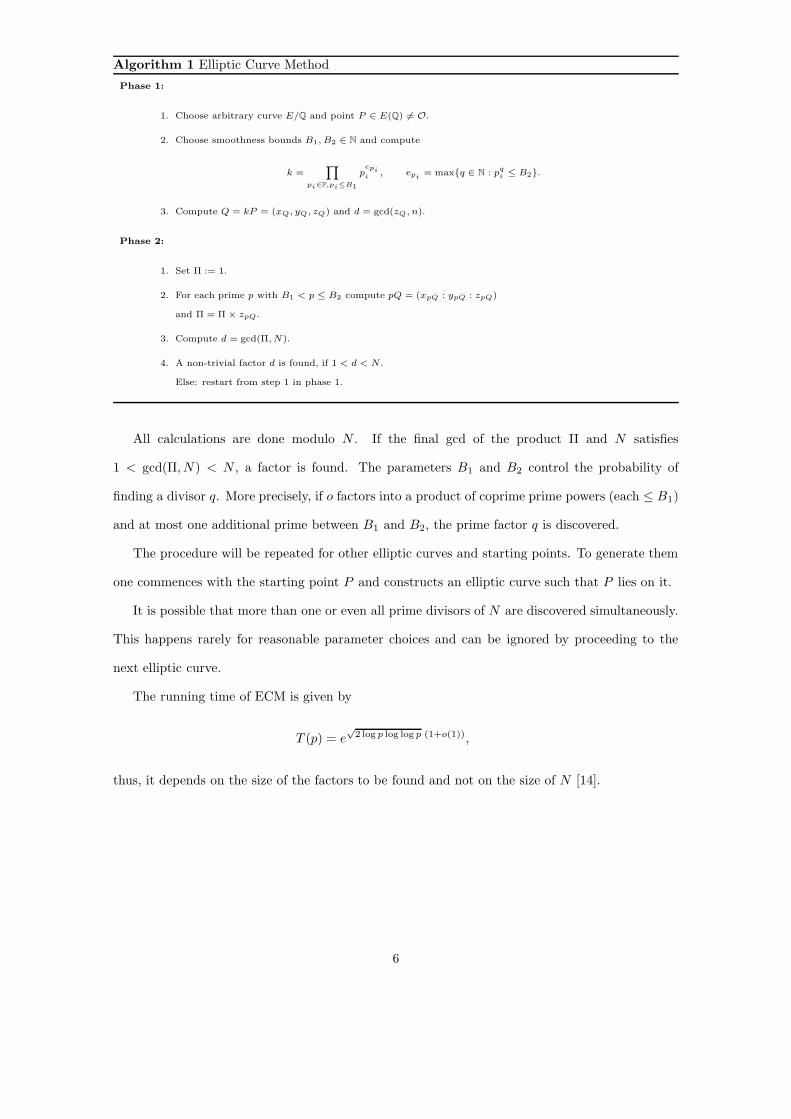
Algorithm 1 Elliptic Curve Method
Phase 1:
1. Choose arbitrary curve E/Q and point P ∈ E(Q) 6= O.
2. Choose smoothness bounds B1, B2 ∈ N and compute
k =Y
pi∈P,pi≤B1
pepii
, epi= max{q ∈ N : pq
i ≤ B2}.
3. Compute Q = kP = (xQ, yQ, zQ) and d = gcd(zQ, n).
Phase 2:
1. Set Π := 1.
2. For each prime p with B1 < p ≤ B2 compute pQ = (xpQ : ypQ : zpQ)
and Π = Π × zpQ.
3. Compute d = gcd(Π, N).
4. A non-trivial factor d is found, if 1 < d < N .
Else: restart from step 1 in phase 1.
All calculations are done modulo N . If the final gcd of the product Π and N satisfies
1 < gcd(Π, N) < N , a factor is found. The parameters B1 and B2 control the probability of
finding a divisor q. More precisely, if o factors into a product of coprime prime powers (each ≤ B1)
and at most one additional prime between B1 and B2, the prime factor q is discovered.
The procedure will be repeated for other elliptic curves and starting points. To generate them
one commences with the starting point P and constructs an elliptic curve such that P lies on it.
It is possible that more than one or even all prime divisors of N are discovered simultaneously.
This happens rarely for reasonable parameter choices and can be ignored by proceeding to the
next elliptic curve.
The running time of ECM is given by
T (p) = e√
2 log p log log p (1+o(1)),
thus, it depends on the size of the factors to be found and not on the size of N [14].
6

3.2 The Elliptic Curves
Apart from the Weierstraß form there are various other forms for the elliptic curves. We use
Montgomery’s form (1) and compute in the set S = E(Z/NZ)/{±1} only using the x- and z-
coordinates.
By2z = x3 + Ax2z + xz2 (1)
It was suggested in [15] by Montgomery. Curves of this form always have an order divisible by
4. I.e., not every curve can be transformed to the Montgomery form. In our case, the curves
can be chosen in such way that they have an order divisible by 12. Appendix A.2 describes the
construction of such curves.
The residue class of P + Q in this set can be computed from P , Q and P − Q using 6 multi-
plications (2). A duplication, i. e. 2P , can be computed from P using 5 multiplications (3). Since
we are only interested in checking whether we obtain the point at infinity for some prime divisor
of N computing in S is no restriction. In the following we will not distinguish between E(Z/NZ)
and S, and pretend to do all computations in E(Z/NZ).
Addition: (2)
xP+Q ≡ zP−Q[(xP − zP )(xQ + zQ) + (xP + zP )(xQ − zQ)]2 (modN)
zP+Q ≡ xP−Q[(xP − zP )(xQ + zQ) − (xP + zP )(xQ − zQ)]2 (modN)
Duplication: (3)
4xP zP ≡ (xP + zP )2 − (xP − zP )2 (modN)
x2P ≡ (xP + zP )2(xP − zP )2 (modN)
z2P ≡ 4xP zP [(xP − zP )2 + 4xP zP (A + 2)/4] (modN)
3.3 The First Phase
If the triple (P, nP, (n+1)P ) is given we can compute (P, 2nP, (2n+1)P ) or (P, (2n+1)P, (2n+2)P )
by one addition and one duplication in Montgomery’s form. Thus Q = kP can be calculated using
[log2 k] additions and duplications according to Algorithm 2, amounting to 11[log2 k] multiplica-
7

tions. In the case zP = 1 we can reduce this to 10[log2 k] multiplications.
Algorithm 2 Exponentiation for Curves in Montgomery Form
INPUT: Basis g ∈ G with g = (gtgt−1 . . . g1g0)2 and a point P on the curve EM : by2 = x3 + ax2 + x.
OUTPUT: Product Q = gP .
1. Pn = P
Pn+1 = 2P
2. for i = t − 1 to 1 do:
(a) if gi = 1, then
Pn = Pn + Pn+1
Pn+1 = 2Pn+1
(b) else
Pn+1 = Pn + Pn+1
Pn = 2Pn
3. if g0 = 1, then Q = Pn + Pn+1
4. else Q = 2Pn.
5. return Q
By handling each prime factor of k separately and using optimal addition chains the number
of multiplications can be decreased to roughly 9.3[log2 k] (see [15]). The addition chains can be
precalculated.
3.4 The Second Phase
The standard way to calculate the points pQ for all primes B1 < p ≤ B2 is to precompute a
(small) table of multiples kQ where k runs through the differences of consecutive primes in the
interval ]B1, B2]. Then, p0Q is computed with p0 being the smallest prime in that interval and the
corresponding table entries are added successively to obtain pQ for the next prime p. Two major
improvements have been proposed for ECM ([16, 15]). Using Montgomery’s form, the procedure
is difficult to implement but can be improved as follows.
The improved standard continuation uses a parameter 2 < D < B1. First, a table T of multiples
kQ of Q for all 1 ≤ k < D2 , gcd(k, D) = 1 is calculated. Each prime B1 < p ≤ B2 can be written
as mD ± k with kQ ∈ T . Now, with Lemma 1 (Appendix A.3), gcd(zpQ, N) > 1 if and only if
gcd(xmDQzkQ − xkQzmDQ, N) > 1. Thus, we calculate the sequence mDQ (which can easily be
8
done in Montgomery’s form) and accumulate the product of all xmDQzkQ − xkQzmDQ for which
mD − k or mD + k is prime.
The memory requirements for the improved standard continuation are ϕ(D)2 points for the table
T and the points DQ, (m−1)DQ, mDQ for computing the sequence, altogether ϕ(D)+6 numbers.
The computational costs consist of the generation of T and the calculation of mDQ which amounts
to at most D4 + B2
D + 7 elliptic curve operations (mostly additions) and at most 3(π(B2)− π(B1))
modular multiplications, π(x) being the number of primes up to x. The last term can be lowered if
D contains many small prime factors since this will increase the number of pairs (m, k) for which
both mD − k and mD + k are prime. Neglecting space considerations a good choice for D is a
number around√
B2 which is divisible by many small primes.
4 Methodology
We will now discuss the parameterization of ECM, optimized for our purposes. Finally, the design
of the ECM unit is described.
4.1 Parameterization of the ECM Algorithm
Our implementation focusses on the factorization of numbers up to 200 bits with factors of up
to around 40 bits. Thus, “good” parameters for B1, B2, and D have to be found, yielding a high
probability of success and a relatively small running time and area consumption. With the running
time depending on the size of the (unknown) factors to be found, optimal parameters cannot be
known beforehand. Hence, good parameters can be found by experiments with different prime
bounds.
Deduced from software experiments, we choose B1 = 960 and B2 = 57.000 as prime bounds.
The value of k has 1375 bits, hence, assuming the binary method (Algorithm 2), 1374 point
additions and point duplications for the execution of phase 1 are required. Due to the use of
Montgomery coordinates, the coordinate zP of the starting point P can be set to 1, thus, addition
takes only 5 multiplications instead of 6. The improved phase 1 (with optimal addition chains) has
to use the general case, where zP 6= 1. For the sake of simplicity and a preferably simple control
logic, we choose the binary method for the time being. For the chosen parameters, the computa-
9

tional complexity of phase 1 is 13740 modular multiplications and squarings1. (With optimized
addition chains this number can be reduced to approximately 12000 modular multiplications and
squarings.)
According to Equation (3), duplicating a point 2PA = PC involves the input values xA, zA, A24
and N , where A24 = (A + 2)/4 is computed from the curve parameter A (see Equation (1)) in
advance and should be stored in a fixed register. A point addition PC = PA +PB handles the input
values xA, zA, xB , zB , xA−B , zA−B and N (see Equation 2). Notice that during phase 1 the values
N, A24, xA−B and zA−B do not change. Furthermore, zA−B = z1 can be chosen to be 1. Thus, no
register is required for zA−B . The output values xC and zC can be written to certain input registers
to save memory. If we assume that the ECM unit does not execute addition and duplication in
parallel, at most 7 registers for the values in Z/nZ are required for phase 1. Additionally, we will
require 4 temporary registers for intermediate values. Thus, a total of 11 registers is required for
phase 1.
For the prime bounds chosen, 5621 primes p ∈ [B1, B2] have to be tested in phase 2. With
the prime bounds fixed, the computational complexity depends on the size of D. Hence, D should
consist of small primes in order to keep ϕ(D) as small as possible. We consider the cases D = 6,
D = 30, D = 60 and D = 210. The initial values can be computed by first computing Q =
DQ, then B1
D Q with the binary method, yielding automatically (B1
D − 1)Q. The total number of
modular multiplications is determined by the number of point additions, point duplications and
multiplications for the product Π. Table 1 displays the computational complexity and the number
of registers required additionally for phase 2. For the numbers in the table, we assume the use of
Algorithm 2 for computing the initial values. E.g., in the case D = 30, the cost for the computation
of DQ, (B1
D − 1)DQ, and B1
D DQ is as much as 8 point additions and 8 point duplications. For the
same D, the computation of the table involves 5 point additions and 2 point duplications, yielding
to a total of 13590 modular multiplications.
Remark: for the case D = 210, we start with B1 = 1050 in order to assure that D and B1 share
the same prime factors.
For phase 2 we choose D = 30 to obtain a minimal AT product of the design. Since ϕ(D) = 8 is
small, only 8 additional registers are required to store all coordinates in a table. Unlike in phase 1,
1In this contribution, squarings and multiplications are considered to have an identical complexity since the
hardware will compute a squaring with the multiplication circuit.
10

Table 1: Computational Complexity and Memory Requirements for Phase 2 depending on D
number of modular multiplications for number
D point additions point duplications product Π total of regs.
6 (9 + 0 + 9340)× 6 = 56094 (9 + 0) × 5 = 45 14625 70764 4
30 (8 + 5 + 1868)× 6 = 11286 (8 + 2) × 5 = 50 13590 24926 10
60 (8 + 9 + 934)× 6 = 5706 (8 + 2) × 5 = 50 13629 19385 18
210 (9 + 28 + 266) × 6 = 1818 (9 + 5) × 5 = 70 13038 14926 50
we have to consider the general case for point addition where zA−B 6= 1. Hence, an additional
register for this quantity is needed. For the product Π of all xA×zB−zA×xB , one more register is
necessary. The temporary registers from phase 1 suffice to store the intermediate results xA × zB ,
zA × xB and xA × zB − zA × xB . Hence, additional 10 registers for phase 2 yield to a total of
21 required registers for both phases. The computational complexity of phase 2 is 1881 point
additions 10 point duplications. Together with the 13590 modular multiplications for computing
the product Π, 24926 modular multiplications and squarings are required.
For a high probability of success (> 90%) for the parameters given, software experiments
suggest to run ECM on approximately 20 different curves.
4.2 Design of the ECM Hardware
The ECM unit mainly consists of three parts: the ALU (Arithmetic Logic Unit), the memory part
(register) and an internal control logic (see Figure 1). Each unit has a very low communication
overhead since all results are stored inside the unit during computation. Before the actual com-
putation starts, all required initial values (xP , N, A24) are assigned to memory cells of the unit.
Only at the very end when the product Π has been computed, the result is read from the unit’s
memory. Commands are generated and timed by a central control logic outside the ECM unit(s).
4.2.1 Central Control Logic
The central control logic is connected to each ECM unit via a control bus (ctrl). It coordinates the
data exchange with the unit before and after computation and starts each computation in the unit
11

Figure 1: Overview of one ECM Unit
control logicctrl
data
control
central
logic
single ECM unit
memory
ALU
by a special set of commands. The commands contain an instruction for the next computation to
be performed (i.e., add, subtract, multiply, double), including the in- and output registers to be
used (R1-R21). The start of an operation is invoked by setting the start-bit to ’1’.
The control bus has to offer the possibility to specify which input register(s) and which out-
put register is active. Only certain combinations of in- and output registers occur, offering the
possibility to reduce the complexity of the logic and the width of the control bus by compressing
the necessary information. For simplicity and clarity, we skipped the further optimization of the
commands. Instead, we use a clearly understandable structure for the commands. A command
consists of 16 bit which are assigned as follows (LSB is left):
start operation input 1 input 2 output
X XX XXXX XXXX XXXXX
If several ECM units work in parallel, only one central control logic is needed. All commands are
sent in parallel to all units. Only in the beginning and in the end, the unit’s memory cells have
to be written and read out separately. Once the computations in all units finished, an LSB of the
central status register is set to ’0’ to indicate the units’ availability for further commands.
4.2.2 Internal Control Logic
Each unit possesses an internal control logic in order to coordinate the data in- and output from
and to the registers, respectively. Once a command with the corresponding start bit is set, the
computation inside the unit is started. Once the computation is finished, a bit is set to ’1’ to
12

indicate the unit’s availability for further commands. The modular arithmetic is coordinated
inside the ALU and communicated with the internal control logic.
4.2.3 Memory
The addresses specified above refer to relative addresses inside each unit since we want to address
the same register in multiple units in parallel. For reading from/ writing to a single register in
a specific unit, the unit needs to be addressed separately. In combination with a unique address
for each unit, a register has a unique hardware address and can be addressed from outside the
unit. This is imperative since the central control logic writes data to these registers before phase 1
starts and it reads data from one of the registers after phase 2 has been finished. Each register
can contain n bits and is organized in e =⌈
n+1w
⌉
words of size w (see Figure 2). Memory access is
performed word wise. Reasonable values for w are w = 4, 8, 16, 32 but are, though, not mandatory.
Figure 2: Memory Management of the ECM Unit
2
1
0 w bits
w bits
w bits
w bitse
2
1
0 w bits
w bits
w bits
w bitse
21 registers
PSfrag replacements
P1 P21
-
4.2.4 Arithmetic Logic Unit (ALU)
The ALU performs the arithmetic modulo 2N , i.e., modular multiplication, modular squaring,
modular addition and subtraction. Possible benefit from using multiple ALUs in one ECM unit is
discussed in Appendix A.4.
Objectives for the choice of implemented algorithms are mentioned in Subsection 4.3.
13

4.3 Choice of the Arithmetic Algorithms
The main purpose of the design is to synthesize an area-time efficient implementation of ECM.
Hence, all algorithms are chosen to allow for low area and relatively high speed. Low area con-
sumption can be achieved by structures, which allow for a certain degree of serialization and, hence,
do not require much memory. For ECM, we have chosen a set of algorithms which seem to be
very well suited for our purpose. In the following, we briefly describe the algorithms for modular
addition, subtraction, and multiplication to be implemented for the ALU. Squaring is done with
the multiplication circuit since a separate hardware circuit for squaring would increase the overall
AT product. Similarly, subtraction can be computed with a slightly changed adder circuit.
4.3.1 Computing with Montgomery Residues
It is well known that the Montgomery multiplication ([17]) is an efficient method for modular
multiplication. Montgomery’s algorithm replaces divisions by simple shift operations and, thus, is
very efficient in hard- and software. The method is based on a representation of the residue class
modulo the modulus N . The corresponding N − residue of an integer x is defined as
x′ = x × r mod N
where r = 2n with 2n−1 < N < 2n such that gcd(r, N) = 1 (which is always true for N odd).
Since it is costly to switch always between integers and their N−residue and vice versa, we will
perform all computations in the residue class.
4.3.2 Modular Multiplication
An efficient Montgomery multiplier, highly suitable for our design is described in [9]. The presented
multiplier architecture allows for word wise multiplication and is scalable regarding operand size,
word size, and pipelining depth. The internal word additions are performed by simple adders.
Figure 3 shows the architectures of one stage. While in [9] a structure with carry-save adders
and redundant representation of operands has been implemented, we have chosen a configuration
with carry-propagate adders and non-redundant representation that makes possible more effective
implementation especially when target platform supports fast carry chain logic. A detailed analysis
and comparison of both structures can be found in [18].
14

Figure 3: Multiplier Stage with Carry-Propagate Adders and Non-redundant Representation
FA FA FA
FA FA FA
Yw-1(j) Mw-1
(j) Yw-2(j) Mw-2
(j) Y0(j) M0
(j)
Sw-1 (j) Sw-2
(j) S0(j)
qi
xi
Sw-1 (j-1) Sw-2
(j-1) S0 (j-1)
cin1
cin2
cout1
cout2
The depicted hardware performs a slightly modified Multiple Word Radix-2 Montgomery Mul-
tiplication (Algorithm 3). Instead of more expensive word-wise addition in step (a) we have used
only bit operations. In Algorithm 3, word and bit vectors are represented as:
N = (0, N (e−1), . . . , N (1), N (0)); Y = (0, Y (e−1), . . . , Y (1), Y (0)); S = (0, S(e−1), . . . , S(1), S(0));
X = (xn−1, . . . , x1, x0), where words are marked with superscripts and bits are marked with
subscripts.
The final reduction step of originally proposed Montgomery multiplication can be omitted when
the following condition is fulfilled:
4M < 2n.
With bounded input values X, Y < 2M , the output value is also bounded (S < 2M).
According to [9], the number of clock cycles per multiplication is given by Equation (4):
Tmul =
⌈
n
p
⌉
× (e + 1) + 2p (4)
A minimal AT product of the sole multiplier can be achieved with a word width of 8 bits and a
pipelining depth of 1 (w = 8, p = 1, see [9]). However, for our ECM architecture, the AT product
does not only depend on the AT product of the multiplier. In fact, the multiplier only takes a
comparably small part of the overall area. On the other hand, the overall speed relies primarily
on the speed of the multiplier. Thus, we choose a pipelining depth of p = 2 for word width w = 32
bits, in order to achieve a higher speed.
15

Algorithm 3 Multiple Word Radix-2 Montgomery Multiplication [9]
1. S = 0
2. for i = 0 to n − 1 do:
(a) qi := xiY(0)0 + S
(0)0
(b) if qi = 1, then
i. for j = 0 to e do:
A. (Ca, S(j)) := Ca + xiY (j) + M(j)
B. (Cb, S(j)) := Cb + S(j)
C. S(j−1) := (S(j)0
, S(j−1)w−1...1
ii. end for
(c) else
i. for j = 0 to e do:
A. (Ca, S(j)) := Ca + xiY (j)
B. (Cb, S(j)) := Cb + S(j)
C. S(j−1) := (S(j)0
, S(j−1)w−1...1
ii. end for
(d) end if
(e) S(e) = 0
3. end for
4.3.3 Modular Addition and Subtraction
Addition and subtraction is implemented as one circuit. As with the multiplication circuit, the
operations are done word wise and the word size and number of words can be chosen arbitrary.
Since the same memory is used for input and output operands, we choose the same word size as for
the multiplier. The subtraction relies on the same hardware, only one input bit has to be changed
(sub = 1) in order to compute a subtraction rather than an addition (see Figure 4, FA denotes a
full adder). All operations are done modulo 2N .
Figure 4: Addition and Subtraction Circuit
FA FA FA FA
PSfrag replacements
sub
x0x1x2xw−1
y0y1y2yw−1
z0z1z2zw−1
c0c1c2cw−1
cin
16

The actual computation is done in a word wise manner using a word size of w = 32. Algo-
rithms 4 and 5 show the elementary steps of a modular addition and subtraction, respectively.
If |x + y| < 2N a reduction can be applied by simple subtraction of twice the modulus 2N .
Hence, following algorithm is used for the modular addition:
Algorithm 4 Modular additionINPUT: Two integers x, y < 2N
OUTPUT: Sum z = x + y mod 2N
1. z = x + y
2. T = z − 2N
3. if T ≥ 0 then z = T
4. return z
z contains the result and T is a (temporary) register. A comparison z < 2N takes the same
amount of time than a subtraction T = z − 2N . Thus, we compute the subtraction in all cases
and decide by the sign of the values, which one to take as the result (z or T ). If T is the correct
result, the content of T has to be copied to the register z.
For a modular addition, we need at most
Tadd = 3 × (e + 1) (5)
clock cycles, where e is the number of words (for implemented non-redundant form of operands
e =⌈
n+1w
⌉
). On average, we would only have to reduce every second time. However, since the
control of phase 1 and phase 2 is parallelized for many units, we have to assume the worst case
running time which is given by Equation (5).
The subtraction x−y can be accomplished by the addition of x with the bitwise complement of
y and 1. The addition of 1 is simply achieved by setting the first carry bit to one (c = 1) (Step 1).
Since the result can be negative, a final verification is required. If necessary, the modulus has to
be added. Following algorithms describes the modular subtraction:
In step 1, both memory cells z and T obtain the same value, which can be done in hardware in
parallel at the same time without any additional overhead. After the computation of the difference,
one can check for the correctness of the result.
17

Algorithm 5 Modular subtractionINPUT: Two integers x, y < 2N
OUTPUT: Difference z = x − y mod 2N
1. T = z = x − y
2. if z < 0 then z = T + 2N
3. return z
Hence, subtraction can be performed more efficiently than addition and requires in the worst
case
Tsub = 2 × (e + 1) (6)
clock cycles.
4.4 Parallel ECM
ECM can be perfectly parallelized by using different curves in parallel since the computations of
each unit are completely independent. For the control of more than one ECM unit, it is essential
to know that both phases, phase 1 and phase 2, are controlled completely identical, independent
of the composite to be factored. Figure 5 shows the control of several ECM units in parallel.
Figure 5: Parallel ECM
control
central
logic
control logic
single ECM unit
memory
ALU
control logic
single ECM unit
memory
ALU
control logic
single ECM unit
memory
ALU
ctrl
data
Solely the curve parameter and eventually the modulus of the units and, hence, the coordinates
of the initial point differ. Thus, all units have to be initialized differently which is done by simply
writing the values into the corresponding memory locations sequentially. During the execution of
18
both phases, exactly the same commands can be sent to all units in parallel. Since running time
of multiplication/squaring is constant (does not rely on input values) and for addition/subtraction
differs at most in 2(e + 1) clock cycles, all units can execute the same command at exactly the
same time. After phase 2, the results are read from the units one after another. The required
time for this data I/O is neglectable for one ECM unit since the computation time of both phases
dominates. For several units in parallel, the computation time does not change, but the time for
data I/O scales linearly with the number of units. Hence, not too many units should be controlled
by one single logic. For massively parallel ECM in hardware, the ECM units can be segmented
into clusters, each with an own control unit.
5 Implementation
This section presents the actual hardware implementation done on a system-on-chip (FPGA and
embedded microprocessor). This first hardware implementation of ECM is designed as a proof-of-
concept. Remark, that all timings are obtained by using real hardware, not only simulation.
5.1 Hardware Platform
The ECM implementation is realized as a hybrid design. It consists of an ECM unit implemented
on an FPGA (Xilinx Virtex2000E-6) and a control logic implemented in software on an embedded
microcontroller (ARM7TDMI, 25MHz). For more information on the hardware platform used, the
interested reader is referred to [19]. The ECM unit is coded in VHDL and was synthesized for a
Xilinx FPGA (Virtex2000E-6, see [20]). For the actual VHDL implementation, memory cells have
been realized with the FPGA’s internal block RAM. For simulation, ModelSim was used, synthesis
and place&route was done using FPGA Advantage’s RTL tools.
The unit, as implemented, listens for commands which are written to control register accessible
by the FPGA. Required point coordinates and curve parameters are loaded into the unit before
the first command is decoded. For this purpose, these memory cells are accessible from the outside
by a unique address. Internal registers, which are only used as temporary registers during the
computation are not accessible from the outside.
The control of the unit is done by the microcontroller present on the board and controls the
data transfer from and to the units, and issues the commands for all steps in phase 1 and phase 2.
19

For code generation, debugging and compilation, the ARM Developer Suite 1.2 was used. For
details on the ARM microprocessor, see [21]. At a later stage, a soft coded processor core (in
VHDL) could be used instead an ARM microprocessor.
The actual design was done for n = 198 bit composites. The parameters for the multiplier are
p = 2 and w = 32. Scaling the design to bit lengths from 100 to 300 bits can be easily accomplished.
In this case, the AT product will de-/ increase according to the size of n2.
5.2 Results
After the synthesis and place and route, the binary image was loaded onto the FPGA and clocked
with a frequency of 25MHz. Hence, the cycle length of the ALU performing the modular arithmetic
is 40ns. Table 2 shows the timings of relevant operations of the implementation. The timings of
both phases include the time required for data I/O. For the FPGA used, the actual design has
a maximum clock frequency of approximately 38MHz. Due to the limits of the board’s clock
generation capabilities, only 25MHz are applied for our timing analysis.
Table 2: Running Times of the ECM Implementation (198 bits modulus), p = 2, w = 32 (Xilinx
Virtex2000E-6 and ARM7TDMI, 25MHz)
Operation Time
modular addition 2.16µs
modular subtraction 2.00µs
modular multiplication 64.5µs
modular squaring 64.3µs
point addition (phase 1, zQ = 1) 334µs
point addition (phase 2) 399µs
point duplication 331µs
Phase 1 918ms
Phase 2 (estimate) 1760ms
20

Although a squaring is computed with the multiplication circuit, the overhead is slightly lower
yielding a mere 0.3% faster execution. Point addition in phase 1 is more efficient since it makes
use of the fact, that the z coordinate of the difference of points can be chosen to be 1.
Remark, that the work on phase 2 is still in progress. Though the FPGA part of phase 2 has
been completed, the complicated control logic has still to be optimized and partially revised. Parts
of phase 2 are already running on the platform, some parts are in progress. Hence, we provide an
estimate of the running time based on the running time of the timings given in Table 2. Based
on experience from the complete hardware implementation of phase 1, we believe this estimate is
fairly accurate.
The ECM unit including the full support for the phase 1 and 2 of the ECM with the word width
w = 32 bits, number of words e = 7, level of pipeline p = 2 has the following area requirements:
1754 LUTs, 506 flip-flops and 44 Blocks RAM. Minimum clock period is 26.225ns (maximum clock
frequency: 38.132MHz). Further improvements in data organization inside the ECM unit should
yield higher performance of the whole design.
Due to the system’s latency for loading and storing values in the registers, not more than 100
ECM units (FPGA) should be controlled by one processor. With a much higher number of units
the communication overhead would outweigh the computation time. However, the control logic of
the data I/O has not been in the focus of our optimization efforts yet and, thus, we assume that
slight improvements of the speed of the data I/O are still feasible. Especially if targeting an ASIC
implementation, such numbers are likely to change.
6 A Case Study: Supporting GNFS with ECM ASICs
Building an efficient and cheap ECM hardware can influence the overall performance of the GNFS
since ECM can be perfectly used for smoothness testing within the GNFS (see [5]). In this section,
we briefly estimate the costs, space requirements and power consumption of a special ECM hard-
ware as ASIC. This special hardware could be produced as single ICs (such as common CPUs),
ready for the use in larger circuits. We choose a setting with a word width w = 8 and assume the
use of carry save adders to allow for a higher clock rate (see [9]).
21
6.1 Estimation of the Running Time
We can determine the running time of both phases on basis of the underlying ring arithmetic. The
upper bounds for the number of clock cycles of a modular addition and a modular subtraction are
given in Equations (5) and (6), respectively. A setting with n = 199, w = 8, p = 8, and e = 25
yields Tadd = 3(e + 1) = 78 and Tsub = 2(e + 1) = 52 cycles. According to 4, the implemented
multiplier requires Tmul = 666 cycles. For each operation we should include Tinit = 2 cycles for
initialization of ALU at the beginning of each computation.
For the group operations for phase 1 we obtain
TPadd = 5Tmul + 3Tadd + 3Tsub + 11Tinit = 3742 cycles and
TPdbl = 5Tmul + 2Tadd + 2Tsub + 9Tinit = 3608 cycles
clock cycles. For phase 2, TPadd changes to T ′Padd = 4410 cycles since zA−B 6= 1 in most cases,
hence, we have to take the multiplication with zA−B into account.
The total cycle count for both phases is
TPhase 1 = 1374(TPadd + TPdbl) = 10098900 cycles and
TPhase 2 = 1881T ′Padd + 50TPdbl + 13590Tmul = 17553730 cycles
clock cycles. Excluding the time for pre- and post-processing, a unit needs approximately 27.7×10⁶
clock cycles for both phases on one curve. If we assume a frequency of 500 MHz, such a complex
computation can be performed in approximately 55 ms.
6.2 Estimation of Area Requirements
According to [9]2, the multiplier with w = 8, p = 8 requires 21400 transistors in standard CMOS
technology (assuming 4 transistors per NAND gate). We assume that the circuit for addition and
subtraction can be achieved with at most 1000 transistors. For the memory, we assume (area
expensive) static RAM which requires 25.200 transistors for 21 registers. For the control inside the
unit and the control of the whole circuit, we assume additional 8.000 transistors per ECM unit.
2Remark: The numbers provided in that contribution refer to a multiplier built with carry save adders. Since
we implemented the architecture with carry propagate adders, given numbers are larger (approximately 20%) than
those which would be achieved with our design.
22

Hence, one unit requires approximately 55.600 transistors. Assuming the CMOS technology of a
standard Pentium 4 processor (0.13µm, approx. Mio. 55 transistors), we could fit 990 ECM units
into the area of one standard processor. One ECM unit needs an area of approximately 0.1475mm2
and has a power dissipation of approximately 40mW.
6.3 Application to the GNFS
Considering the architecture for a special GNFS hardware of [5], we have to test approximately
1.7 × 10¹⁴ rests up to 125 bits for smoothness. Since both the running time as well as the area
requirement scales linearly with the bit size, we can multiply the results from the subsections above
with a factor of 125/198 ≈ 0.628. If we distribute the computation over a whole year, we have to
check 5.390.665 rests per second.
For a probability of success of > 90%, we test 20 curves per rest, thus, we need approximately
3.850.000 ECM units which would yield a total chip area of 625.000mm2 (= 4300 ICs of the size of
a Pentium 4) and a power consumption of approximately 175 kW. If we assume a cost of $ 5.000
per 300mm wafer, as done in [6], the ECM units would cost less than $ 45.000 for the whole GNFS
architecture, which is neglectable in the context of the overall costs.
7 Conclusions
With the work on hand, we present a thorough analysis of adequate algorithms for an ECM hard-
ware architecture. The parameterization of the algorithms was done to particularly fit the needs of
a hardware environment, yielding a high efficiency regarding the area-time product. Furthermore,
this is the first publication showing a real hardware implementation of the ECM algorithm. The
implementation is a hardware-software Co-design and has been implemented on an FPGA and an
ARM microcontroller for factoring integers of a size of up to 198 bits. We implemented a variant
of ECM which allows for a very low area time product and, hence, is very cost effective. Our im-
plementation impressively shows that due to very low area requirements and low data I/O, ECM
is predestined for the use in hardware. A single unit for factoring composites of up to 198 bits
requires 506 flip-flops, 1754 lookup-tables and 44 BlockRAMs (less than 6% of logic and 27% of
memory resources of the Xilinx Vertex2000E device). Regarding a possible ASIC implementation,
around 990 ECM units could be placed on a single Pentium4-sized chip.
23

As demonstrated, ECM can be perfectly parallelized and, thus, an implementation at a larger
scale can be used to assist the GNFS factoring algorithm by carrying out all required smoothness
tests. A low cost ASIC implementation of ECM can decrease the overall costs of the GNFS archi-
tecture SHARK, as shown in [5]. We believe that an extensive use of ECM for smoothness testing
can further reduce the costs of such a GNFS machine.
As future steps, the control logic for the second phase will be finalized. Variants of phase 2
can be examined in order to achieve the lowest possible AT product. To achieve a higher maximal
clock frequency of the ECM unit, the control logic inside the unit might be optimized.
Since most of the computation time is spent for modular multiplications, an improvement of the
implementation of the multiplication directly affects the overall performance. Hence, alternative
architectures for the multiplication can be investigated.
With the VHDL source code at hand, the next logic step is the design and simulation of
a full custom ASIC containing the logic, which currently is implemented in the FPGA. For an
ASIC implementation, a parallel design of many ECM units is preferable. The control can still
be handled outside the ASIC by a small microcontroller, as it is the case with the work at hand.
Alternatively, a soft core of a small microcontroller can be adopted to the specific needs of ECM
and be implemented within the ASIC. With a running ECM ASIC, exact cost estimates for the
support of algorithms such as the GNFS can be obtained.
References
[1] R. L. Rivest, A. Shamir, and L. Adleman, “A Method for Obtaining Digital Signatures and
Public-Key Cryptosystems,” Communications of the ACM, vol. 21, pp. 120–126, February
1978.
[2] H. W. Lenstra, “Factoring Integers with Elliptic Curves,” Annals of Mathematics, vol. 126,
no. 2, pp. 649–673, 1987.
[3] A. K. Lenstra and H. W. Lenstra, The Development of the Number Field Sieve. Lecture Notes
in Math. Volume 1554, 1993.
24

[4] J. Franke, T. Kleinjung, F. Bahr, M. Lochter, and M. Bohm, “E-mail announcement.”
http://www.crypto-world.com/announcements/rsa576.txt, December 2003.
[5] J. Franke, T. Kleinjung, C. Paar, J. Pelzl, C. Priplata, and C. Stahlke, “SHARK — A Realiz-
able Special Hardware Sieving Device for Factoring 1024-bit Integers.” Submitted to SHARCS
2005 — Special-purpose Hardware for Attacking Cryptographic Systems, December 2004.
[6] A. Shamir and E. Tromer, “Factoring Large Numbers with the TWIRL Device,” in Advances
in Cryptology — Crypto 2003, vol. 2729 of LNCS, pp. 1–26, Springer, 2003.
[7] G. Orlando and C. Paar, “A Scalable GF (p) Elliptic Curve Processor Architecture for Pro-
grammable Hardware,” in Workshop on Cryptographic Hardware and Embedded Systems —
CHES 2001 (C. K. Koc, D. Naccache, and C. Paar, eds.), vol. LNCS 2162, pp. 348–363,
Springer-Verlag, May 14-16, 2001.
[8] N. Gura, S. Chang, H. 2, G. Sumit, V. Gupta, D. Finchelstein, E. Goupy, and D. Stebila, “An
End-to-End Systems Approach to Elliptic Curve Cryptography,” in Cryptographic Hardware
and Embedded Systems — CHES 2002 (C. K. Koc and C. Paar, eds.), vol. LNCS 2523,
pp. 349–365, Springer-Verlag, 2002.
[9] A. Tenca and C.K. Koc, “A Scalable Architecture for Modular Multiplication Based on Mont-
gomery’s Algorithm,” IEEE Trans. Comput., vol. 52, no. 9, pp. 1215–1221, 2003.
[10] D. Bernstein, “Circuits for Integer Factorization: A Proposal.” Manuscript.
Available at http://cr.yp.to/papers.html#nfscircuit, 2001.
[11] E. Wolski, J. G. S. Filho, and M. A. R. Dantas, “Parallel Implementation of Elliptic Curve
Method for Integer Factorization Using Message-Passing Interface (MPI),” in SBAC- PAD
13th Symposium on Computer Architecture and High-Performance, 2001, Pirenopolis - GO.
SBAC- PAD 13th Symposium on Computer Architecture and High-Performance, 2001.
[12] P. Zimmermann, “ECMNET page.” Available at
http://www.loria.fr/~zimmerma/records/ecmnet.html.
[13] J. Pollard, “A Monte Carlo Method for Factorization,” Nordisk Tidskrift for Informationsbe-
handlung (BIT), vol. 15, pp. 331–334, 1975.
25

[14] R. P. Brent, “Factorization of the tenth Fermat number,” Mathematics of Computation,
vol. 68, no. 225, pp. 429–451, 1999.
[15] P. Montgomery, “Speeding up the Pollard and elliptic curve methods of factorization,” Math-
ematics of Computation, vol. 48, pp. 243–264, 1987.
[16] R. P. Brent, “Some Integer Factorization Algorithms Using Elliptic Curves,” in Australian
Computer Science Communications 8, pp. 149–163, 1986.
[17] P. Montgomery, “Modular Multiplication without Trial Division,” Mathematics of Computa-
tion, vol. 44, pp. 519–521, April 1985.
[18] M. Drutarovsky, V. Fischer, and M. Simka, “Comparison of two implementations of scalable
Montgomery coprocessor embedded in reconfigurable hardware,” in Proceedings of the XIX
Conference on Design of Circuits and Integrated Systems – DCIS 2004, (Bordeaux, France),
pp. 240–245, Nov. 24–26, 2004.
[19] NEC Corporation, “Preliminary User’s Manual System-on-Chip Lite, Development Board,
Hardware, Document No. A15650EE1V0UM00,” July 2001.
Available at http://www.ee.nec.de/_pdf/A15650EE1V0UM00.PDF.
[20] Xilinx, “Virtex-E 1.8V Field Programmable Gate Arrays — Production Product Specifica-
tion.” http://www.xilinx.com/bvdocs/publications/ds022.pdf, June 2004.
[21] ARM Limited, “ARM7TDMI (Rev 3) — Technical Reference Manual.” Available at
http://www.arm.com/pdfs/DDI0029G_7TDMI_R3_trm.pdf, 2001.
[22] A. O. L. Atkin and F. Morain, “Finding suitable curves for the elliptic curve method of
factorization,” Mathematics of Computation, vol. 60, no. 201, pp. 399–405, 1993.
26

A Appendix
A.1 Pollard’s (p − 1)-algorithm
Let k, N ∈ N with N being the composite to be factored. Furthermore, q|N with q ∈ P. Let a ∈ Z
be coprime to N , i.e., gcd(a, N) = 1. Let e = k(q − 1).
By little Fermat,
aq−1 ≡ 1 mod q ⇒ ak(q−1) ≡ 1 mod q
⇔ ae − 1 ≡ 0 mod q
⇐ q|ae − 1.
q|N yields gcd(ae − 1, N) > 1.
If ae 6≡ 1 mod N then 1 < ggT (ae − 1, N) < N.
In this case, we found a non-trivial divisor of N .
We cannot compute e = k(q − 1) since q is unknown. Instead, we assume that q − 1 can
be decomposed into many small factors below a certain threshold B1. The highest prime power
dividing q − 1 is denoted as B2. q − 1 is then called (B1, B2)-smooth. Now, choose e such that
e =∏
pi∈P,pi≤B1
pepi
i , epi= max{q ∈ N : pq
i ≤ B2}.
Hopefully, the computation of ae with d = ggT (ae − 1, N) yields a non-trivial factor d of N .
Generally, Pollard’s method can be defined as follows:
Let Gq := (Z/qZ)? and GN := (Z/NZ)? be multiplicative groups and let GN → Gq , a → a be the
reduction modulo q. A factor of N is found, if ae 6≡ 1 mod N and ae ≡ 1 mod q, i.e.,
∀k1 ∈ N : e 6= k1 × o(a),
∃k2 ∈ N : e = k2 × o(a)
with o being the order of an element.
27

A.2 Finding Suitable Curves in Montgomery Form
Assume a curve of the form
By2 = x3 + Ax2 + x with gcd((A2 − 4)B, n) = 1.
Such curves have a group order divisible by 4.
To obtain an order divisible by 12, choose A and B such, that
A =−3a4 − 6a2 + 1
4a3, B =
(a2 − 1)2
4a3
with a =t2 − 1
t2 + 3.
The point
(x0, y0) =
(
3a2 + 1
4a,
√3a2 + 1
4a
)
is on the curve, if 3a2 + 1 = 4(t4 + 3)/(t2 + 3)2 is a rational square, which can be obtained by
t2 = (u2 − 12)/4u and u3 − 12u being a rational square. It is also possible to find suitable curves
with torsion groups of order of 16 (see [22, 15]) but yield no noticeable performance increase for
our application.
A.3 Useful Propositions
Following Lemma allows us to reduce the complexity by repeatedly multiplying a difference of two
products instead of computing complex point operations each step:
Lemma 1 Let q = a + b with a and b coprime (which is true for any prime p). Furthermore, let
qQ = A + B with A = aQ and B = bQ, then zqQ = 0 mod t for gcd(zQ, n) = 1 if and only if
xA × zB − zA × xB ≡ 0 mod t.
Proof
1. Montgomery’s point addition formula yields
t|zqQ ⇔ t|xA−B [xA × zB − zA × xB ]2
⇐ t|(xA × zB − zA × xB).
28

2. if zqQ ≡ 0 mod t, qQ is the identity point on the elliptic curve over Ft. Hence, A = −B, i.e.
A and B are zero or
xA/zA ≡ xB/zB mod t.
A = B = 0 yields Q = 0, thus t|zQ, which is a contradiction to the assumption of gcd(zQ, n) =
1. Then we have
xA/zA ≡ xB/zB mod t and
xA × zB ≡ zA × xB mod t respectively.
A.4 Use of Multiple ALUs
In this subsection, we will discuss the influence of using more than one ALU on the execution time
and area of both phases. We have to find a trade-off between lowering the overall execution time
and increasing area. Obviously, a naive approach would be the parallel use of 10 ALUs instead of
one to compute every multiplication in parallel. But most operations depend on previously made
computations and are, thus, not completely parallizable. Even if some operations are parallizable,
their results have to be stored for post-processing, hence, more registers are required.
Typical operations during phase 1 are the point operations point addition and point duplication.
Table 3 shows the sequence of required computations for a point addition (with zP = 1, as imple-
mented for phase 1). The operations for multiplication, addition and subtraction are denoted as
mul, add and sub, whereas the output operand is the first argument and the two input arguments
are at the second and last position. Ti are temporary registers. We identify at most two indepen-
dent multiplication operations in this operation, i.e., before starting with the multiplications 9 and
10, the results of the multiplications from steps 3 and 6 (and some additions and subtractions)
have to be available.
Hence, at most two ALUs can significantly improve the execution time of phase 1. Table 4
shows the parallelized sequence of the point addition for two ALUs. In step 6 we can see ALU 1
running idle for the time of a multiplication since the point addition algorithm cannot be optimal
parallelized. If we neglect the time for addition and subtraction, we can reduce the execution time
by 40%. The number of temporary registers increases by 50% from 4 to 6.
The Table 5 and 6 show the computations for a point duplication with 1 and 2 ALUs, re-
spectively. Similar to point addition, we cannot manage an optimum parallization since ALU 1 is
29

Table 3: Point Addition with 1 ALU (Pseudocode)
Step ALU 1
1 sub(T1, xP1, zP1)
2 add(T2, xP2, zP2)
3 mul(T3, T1, T2)
4 add(T1, xP1, zP1)
5 sub(T2, xP2, zP2)
6 mul(T4, T1, T2)
7 add(T1, T3, T4)
8 sub(T2, T3, T4)
9 mul(xP1+P2, T1, T1)
10 mul(T3, T2, T2)
11 mul(zP1+P2, xP1−P2, T3)
P
tsum ≈ 6 × tadd + 5 × tmul
Table 4: Point Addition with 2 ALUs (Pseudocode)
Step ALU 1 ALU 2
1 sub(T1, xP1, zP1) add(T4, xP1, zP1)
2 add(T2, xP2, zP2) sub(T5, xP2, zP2)
3 mul(T3, T1, T2) mul(T6, T4, T5)
4 add(T1, T3, T6) sub(T2, T3, T6)
5 mul(xP1+P2, T1, T1) mul(T3, T2, T2)
6 mul(zP1+P2, xP1−P2, T3)
P
tsum ≈ 3 · (tadd + tmul)
running idle for some time.
The overall running time in the parallelized algorithm can be reduced by approximately 40%,
the number of required registers for intermediate results stays constant.
Phase 2, parameterized according to Section 4.1, is more complicated to parallelize. All point
operations can be parallelized as described above. The computations for the product involve three
multiplications, where two can be executed in parallel. Hence, an acceleration of approximately
35% can be achieved with two ALUs3.
Combining both phases, two ALUs yield a total speed up of 37%. Hence, the AT product of
two ALUs is higher than that of a single ALU. Additionally, two more registers for intermediate
3Remark: A slightly improved acceleration could be attained by investigating a higher degree of optimization by
interleaving parts of the operations.
30

Table 5: Point Duplication with 1 ALU (Pseudocode)
Step ALU 1
1 add(T1, xP , zP )
2 sub(T2, xP , zP )
3 mul(T3, T1, T1)
4 mul(T4, T2, T2)
5 sub(T1, T3, T4)
6 mul(T2, T1, A24)
7 mul(x2P , T3, T4)
8 add(T3, T2, T4)
9 mul(z2P , T1, T3)
P
tsum ≈ 4 · tadd + 5 · tmul
Table 6: Point Duplication with 2 ALUs (Pseudocode)
Step ALU 1 ALU 2
1 add(T1, xP , zP ) sub(T2, xP , zP )
2 mul(T3, T1, T1) mul(T4, T2, T2)
3 sub(T1, T3, T4)
4 mul(T2, T1, A24) mul(x2P , T3, T4)
5 add(T3, T4, T2)
6 mul(z2P , T1, T3)
P
tsum ≈ 3 · tadd + 3 · tmul
values are required. However, considering the AT complexity of the entire ECM unit, the AT
product does slightly decrease. The reason for this behavior is the impact of the area due to the
21 registers of the unit. An additional ALU and 2 more registers only slightly influence the total
area consumption, hence, yielding a lower AT product.
31

List of Figures
1 Overview of one ECM Unit . . . . . . . . . . . . . . . . . . . . . . . . . . . . . . . 12
2 Memory Management of the ECM Unit . . . . . . . . . . . . . . . . . . . . . . . . 13
3 Multiplier Stage with Carry-Propagate Adders and Non-redundant Representation 15
4 Addition and Subtraction Circuit . . . . . . . . . . . . . . . . . . . . . . . . . . . . 16
5 Parallel ECM . . . . . . . . . . . . . . . . . . . . . . . . . . . . . . . . . . . . . . . 18
32