Embed Size (px)
Citation preview

Mahyar SHAHSAVARILille University of Science and Technology
Doctoral Thesis
Unconventional Computing Using MemristiveNanodevices: From Digital Computing to
Brain-like Neuromorphic Accelerator
Supervisor: Pierre BOULET
Thèse en vue de l’obtention du titre de
Docteur en
INFORMATIQUE
DE L’UNIVERSITÉ DE LILLEÉcole Doctorale des Sciences Pour l’Ingénieur de Lille - Nord De France
14-Dec-2016
Jury:
Hélène Paugam-Moisy Professor of University of the French West Indies (Université des Antilles), France (Rapporteur)Michel Paindavoine Professor of University of Burgundy (Université de Bourgogne), France (Rapporteur)Virginie Hoel Professor of Lille University of Science and Technology, France(Président)Said Hamdioui Professor of Delft University of Technology, The NetherlandsPierre Boulet Professor of Lille University of Science and Technology, France

Acknowledgment
Firstly, I would like to express my sincere gratitude to my advisor Prof. Pierre Boulet for all kind ofsupports during my PhD. I never forget his supports specially during the last step of my PhD that Iwas very busy due to teaching duties. Pierre was really punctual and during three years of differentmeetings and discussions, he was always available on time and as a record he never canceled anymeeting. I learned a lot form you Pierre, specially the way of writing, communicating and presenting.you were an ideal supervisor for me.
Secondly, I am grateful of my co-supervisor Dr Philippe Devienne. As I did not knew any Frenchat the beginning of my study, it was not that easy to settle down and with Philippe supports the lifewas more comfortable and enjoyable for me and my family here in Lille. I have never forgotten ourjoyful time in concert and playing violin with ELV music group, your delicious foods and cakes, visitingLondon, Vienna, Kermanshah and Tehran all nice moments we spended with Philippe. With Philippesupport we started a scientific collaboration with Razy University at my hometown city Kermanshah.We got the Gundishapour grants for two years collaboration between Lille 1 and Razy Universities Inaddition to signing a MoU for long term collaboration between two universities all thanks to Philippeefforts.
I would like to acknowledge and thanks to my thesis committee: Prof. Hélène Paugam-Moisy, Prof.Michel Paindavoine, Prof. Said Hamdioui and the president of the jury, Prof. Virginie Hoel for theirinsightful comments and encouragement, and reviewing my thesis.
My sincere thanks also goes to CRIStAL lab and Émeraude team colleagues, prof. Giuseppe Lipari,Dr Richard Olejnik, Dr Clément Ballabriga and specially to Dr Julien Forget. I will never forget Forgetsupports specially for the first time teaching at Polytech Lille. I appreciate my Émeraude team friendsAntoine Bertout, Khalil Ibrahim Hamzaoui, Houssam Zahaf, Pierre Falez and Yassine sidlakhdar fornice discussions, coffee drinking and playing football together. I would like to thanks to our colleagueDr Fabien Alibart in IEMN lab for his technical consultancy during my research particularly duringdeveloping new synapse. I gratefully acknowledge my previous friends and colleagues in TUDelft inThe Neterlands, my lovely and kind friends Faisal Nadeem, Arash Ostadzadeh, Mahmood Ahmadi thatshared with me valuable knowledge and information. Thanks again to Prof. Said Hamdioui that westarted working on memristor together in CE group at TUDelft.
Special thanks go to my Iranian friends in Lille Farzan, Hamid, Hamidreza, Ehsan, Babak, and Sinathanks for bing there for me. Eric and Leopoled, my lovely officemates and friends, I never forget yourkindnesses in our calm office in M3 building. I am grateful of my Iranian friends and colleagues at RaziUniversity, Prof. Mohsen Hayati Dr Mahmood Ahmadi, Dr Arash Ahmadi and one of my best friendMazdak Fatahi that we started working on neural network research for his Master thesis. We have donemany skype meetings that both of us learned a lot during those scientific discussions. Actually the lastchapter of my thesis is related to his master thesis topic. I appreciate my father in law Prof. MohammadMehdi Khodaei for his guidance during my research as well as supporting us for starting collaborationbetween Razi and Lille 1 universities. I really Dr Mahmood Ahmadi, and Mazdak Fatahi for theirsupports and being kindly present specially during the time our French professors and colleagues
i

visited Kermanshah and Razi university. Without Mahmood helps and supports this collaboration wasnot feasible.
I am very grateful of my close family in Iran, my kind father, my lovely mother and two supportivebrothers Mehdi and Mahziar and my little nephews Abolfazl and Ali who always prayed for me andencouraged me continuously not only during my PhD but also in whole my life.
Last, but not the least, I would like to express my appreciation to my better-half Hanieh, actuallyDr Hanieh Khodaei. She was a kind wife, the best friend that we shared whole the beautiful, sad andeven stressful moments of our PhD together. Thanks for all those understanding and supports. Thebest gift during my PhD was from my Almighty, Hana was my best gift, thanks God. Sorry Hana that Iconsisted part of the time that I should have played with you to my thesis and research.
Be yari Parvardegar YektaMahyar Shahsavari,December 2016
ii

Abstract
By 2020, there will be 50 to 100 billion devices connected to the Internet. Two domains of hot researchto address these high demands of data processing are the Internet of Things (IoT) and Big Data. Thedemands of these new applications are increasing faster than the development of new hardwareparticularly because of the slowdown of Moore’s law. The main reason of the ineffectiveness ofthe processing speed is the memory wall or Von Neumann bottleneck which is comming from speeddifferences between the processor and the memory. Therefore, a new fast and power-efficient hardwarearchitecture is needed to respond to those huge demands of data processing.
In this thesis, we introduce novel high performance architectures for next generation computingusing emerging nanotechnologies such as memristors. We have studied unconventional computingmethods both in the digital and the analog domains. However, the main focus and contribution is inSpiking Neural Network (SNN) or neuromorphic analog computing. In the first part of this dissertation,we review the memristive devices proposed in the literature and study their applicability in a hardwarecrossbar digital architecture. At the end of part I, we review the Neuromorphic and SNN architecture.The second part of the thesis contains the main contribution which is the development of a NeuralNetwork Scalable Spiking Simulator (N2S3) suitable for the hardware implementation of neuromorphiccomputation, the introduction of a novel synapse box which aims at better learning in SNN platforms,a parameter exploration to improve performance of memristor-based SNN, and finally a study of theapplication of deep learning in SNN.
iii


Résumé
On estime que le nombre d’objets connectés à l’Internet atteindra 50 à 100 milliards en 2020. Larecherche s’organise en deux champs principaux pour répondre à ce défi : l’internet des objets etles grandes masses de données. La demande en puissance de calcul augmente plus vite que ledéveloppement de nouvelles architectures matérielles en particulier à cause du ralentissement dela loi de Moore. La raison principale en est est le mur de la mémoire, autrement appelé le gouletd’étranglement de Von Neumann, qui vient des différences de vitesse croissantes entre le processeuret la mémoire. En conséquence, il y a besoin d’une nouvelle architecture matérielle rapide et économeen énergie pour répondre aux besoins énormes de puissance de calcul.
Dans cette thèse, nous proposons de nouvelles architectures pour les processeurs de prochainegénération utilisant des nanotechnologies émergentes telles que les memristors. Nous étudions desméthodes de calcul non conventionnelles aussi bien numériques qu’analogiques. Notre contributionprincipale concerne les réseaux de neurones à impulsion (RNI) ou architectures neuromorphiques.Dans la première partie de la thèse, nous passons en revue les memristors existants, étudions leurutilisation dans une architecture numérique à base de crossbars, puis introduisons les architecturesneuromorphiques. La deuxième partie contient la contribution principale : le développement d’unesimulateur d’architectures neuromorphiques (N2S3), l’introduction d’un nouveau type de synapsepour améliorer l’apprentissage, une exploration des paramètres en vue d’améliorer les RNI, et enfinune étude de la faisabilité des réseaux profonds dans les RNI.
v

Contents
Contents 1
List of Figures 3
List of Tables 7
1 Introduction 91.1 Introduction . . . . . . . . . . . . . . . . . . . . . . . . . . . . . . . . . . . . . . . . . . . . 91.2 Part I:Motivation, state-of-the-art and application of using emerging nanodevices for
unconventional computing . . . . . . . . . . . . . . . . . . . . . . . . . . . . . . . . . . . 101.3 Part II:Our contribution in spiking neural network architecture: Simulator, New synapse
box, Parameter exploration and Spiking deep learning . . . . . . . . . . . . . . . . . . . 111.4 Manuscript outline . . . . . . . . . . . . . . . . . . . . . . . . . . . . . . . . . . . . . . . . 13
I Motivation, state-of-the-art and application of using emerging nanodevices forunconventional computing 15
2 Memristor nanodevice for unconventional computing: review and applications 172.1 Introduction . . . . . . . . . . . . . . . . . . . . . . . . . . . . . . . . . . . . . . . . . . . . 172.2 Memristor device overview and properties . . . . . . . . . . . . . . . . . . . . . . . . . . 18
2.2.1 Memristor a missing electrical passive element . . . . . . . . . . . . . . . . . . . 182.2.2 Memristive device functionality . . . . . . . . . . . . . . . . . . . . . . . . . . . . 192.2.3 Electrical model . . . . . . . . . . . . . . . . . . . . . . . . . . . . . . . . . . . . . 20
2.3 Memristor classification based on different materials and applications . . . . . . . . . 212.3.1 Resistive Memristor . . . . . . . . . . . . . . . . . . . . . . . . . . . . . . . . . . . 222.3.2 Spintronic Memristor . . . . . . . . . . . . . . . . . . . . . . . . . . . . . . . . . . 222.3.3 Organic (Polymeric) Memristor . . . . . . . . . . . . . . . . . . . . . . . . . . . . 232.3.4 Ferroelectric Memristor . . . . . . . . . . . . . . . . . . . . . . . . . . . . . . . . . 252.3.5 Evaluation of Memristor with different materials . . . . . . . . . . . . . . . . . . 25
2.4 Potential applications of memristors . . . . . . . . . . . . . . . . . . . . . . . . . . . . . . 272.4.1 Memristor-based nonvolatile memory . . . . . . . . . . . . . . . . . . . . . . . . 272.4.2 Digital computing . . . . . . . . . . . . . . . . . . . . . . . . . . . . . . . . . . . . 272.4.3 Analog domain applications . . . . . . . . . . . . . . . . . . . . . . . . . . . . . . 28
2.5 Streams of research . . . . . . . . . . . . . . . . . . . . . . . . . . . . . . . . . . . . . . . . 282.6 Conclusions and summary . . . . . . . . . . . . . . . . . . . . . . . . . . . . . . . . . . . . 29
3 Unconventional digital computing approach: memristive nanodevice platform 313.1 Introduction . . . . . . . . . . . . . . . . . . . . . . . . . . . . . . . . . . . . . . . . . . . . 31
1

CONTENTS
3.2 Stateful implication logic . . . . . . . . . . . . . . . . . . . . . . . . . . . . . . . . . . . . . 323.2.1 Functionally complete Boolean operations . . . . . . . . . . . . . . . . . . . . . 33
3.3 Crossbar architecture . . . . . . . . . . . . . . . . . . . . . . . . . . . . . . . . . . . . . . . 343.3.1 Memristive switches in crossbar architectures . . . . . . . . . . . . . . . . . . . . 343.3.2 Configurable crossbar array logic gates . . . . . . . . . . . . . . . . . . . . . . . . 35
3.4 Evaluation . . . . . . . . . . . . . . . . . . . . . . . . . . . . . . . . . . . . . . . . . . . . . 383.5 Conclusions . . . . . . . . . . . . . . . . . . . . . . . . . . . . . . . . . . . . . . . . . . . . 38
4 Neuromorphic computing in Spiking Neural Network architecture 414.1 Introduction . . . . . . . . . . . . . . . . . . . . . . . . . . . . . . . . . . . . . . . . . . . . 414.2 Spiking Neural Networks . . . . . . . . . . . . . . . . . . . . . . . . . . . . . . . . . . . . . 43
4.2.1 Spike information coding . . . . . . . . . . . . . . . . . . . . . . . . . . . . . . . . 434.2.2 Network topology . . . . . . . . . . . . . . . . . . . . . . . . . . . . . . . . . . . . 45
4.3 Spiking neuron model . . . . . . . . . . . . . . . . . . . . . . . . . . . . . . . . . . . . . . 474.3.1 Biological, artificial and spiking neuron . . . . . . . . . . . . . . . . . . . . . . . 47
4.4 Synapse and learning . . . . . . . . . . . . . . . . . . . . . . . . . . . . . . . . . . . . . . . 514.4.1 Synaptic learning and plasticity . . . . . . . . . . . . . . . . . . . . . . . . . . . . 52
4.5 Hardware spiking neural network systems . . . . . . . . . . . . . . . . . . . . . . . . . . . 614.6 Discussion . . . . . . . . . . . . . . . . . . . . . . . . . . . . . . . . . . . . . . . . . . . . . 624.7 Conclusion . . . . . . . . . . . . . . . . . . . . . . . . . . . . . . . . . . . . . . . . . . . . . 64
II Our contribution in spiking neural network architecture: Simulator, New synapsebox, Parameter exploration and Spiking deep learning 65
5 N2S3, an Open-Source Scalable Spiking Neuromorphic Hardware Simulator 675.1 Introduction . . . . . . . . . . . . . . . . . . . . . . . . . . . . . . . . . . . . . . . . . . . . 675.2 Event-Driven Simulation Architecture . . . . . . . . . . . . . . . . . . . . . . . . . . . . . 68
5.2.1 Event-Driven vs Clock-Driven Simulation . . . . . . . . . . . . . . . . . . . . . . 685.2.2 Technological Choices: Scala and Akka . . . . . . . . . . . . . . . . . . . . . . . . 685.2.3 Software Architecture . . . . . . . . . . . . . . . . . . . . . . . . . . . . . . . . . . 69
5.3 Neuron, Synapse, Network Modeling . . . . . . . . . . . . . . . . . . . . . . . . . . . . . . 695.3.1 Neuron Modeling . . . . . . . . . . . . . . . . . . . . . . . . . . . . . . . . . . . . . 695.3.2 Synapse modeling and learning . . . . . . . . . . . . . . . . . . . . . . . . . . . . 705.3.3 Network Topologies . . . . . . . . . . . . . . . . . . . . . . . . . . . . . . . . . . . 71
5.4 N2S3 Features . . . . . . . . . . . . . . . . . . . . . . . . . . . . . . . . . . . . . . . . . . . 725.4.1 Input Processing . . . . . . . . . . . . . . . . . . . . . . . . . . . . . . . . . . . . . 725.4.2 Visualization tools . . . . . . . . . . . . . . . . . . . . . . . . . . . . . . . . . . . . 725.4.3 Experiment Specification Language . . . . . . . . . . . . . . . . . . . . . . . . . . 725.4.4 Software Engineering Practices . . . . . . . . . . . . . . . . . . . . . . . . . . . . 735.4.5 Standard experiments . . . . . . . . . . . . . . . . . . . . . . . . . . . . . . . . . . 73
5.5 Conclusion . . . . . . . . . . . . . . . . . . . . . . . . . . . . . . . . . . . . . . . . . . . . . 75
6 Combining a Volatile and Nonvolatile Memristor in Artificial Synapse to Improve Learn-ing in Spiking Neural Networks 776.1 Introduction . . . . . . . . . . . . . . . . . . . . . . . . . . . . . . . . . . . . . . . . . . . . 776.2 Circuit Design of Neuron and Synapse in RBM Network . . . . . . . . . . . . . . . . . . . 78
6.2.1 Leaky Integrate-and-Fire neurons . . . . . . . . . . . . . . . . . . . . . . . . . . . 786.2.2 New artificial synapse using memristors . . . . . . . . . . . . . . . . . . . . . . . 786.2.3 New plasticity learning method . . . . . . . . . . . . . . . . . . . . . . . . . . . . 796.2.4 Combining a volatile and nonvolatile memristor to make a new artificial synapse 806.2.5 Network topology and learning . . . . . . . . . . . . . . . . . . . . . . . . . . . . 80
2

6.3 Experimental Validation . . . . . . . . . . . . . . . . . . . . . . . . . . . . . . . . . . . . . 816.3.1 MNIST recognition improvement . . . . . . . . . . . . . . . . . . . . . . . . . . . 81
6.4 Conclusion . . . . . . . . . . . . . . . . . . . . . . . . . . . . . . . . . . . . . . . . . . . . . 82
7 Evaluation methodology and parameter exploration to improve performance of memristor-based spiking neural network architecture 857.1 Introduction . . . . . . . . . . . . . . . . . . . . . . . . . . . . . . . . . . . . . . . . . . . . 857.2 Experimental evaluation of the influence of four parameters on the classification of
handwritten digits . . . . . . . . . . . . . . . . . . . . . . . . . . . . . . . . . . . . . . . . . 877.2.1 Effect of spike distribution . . . . . . . . . . . . . . . . . . . . . . . . . . . . . . . 887.2.2 Effect of STDP window duration . . . . . . . . . . . . . . . . . . . . . . . . . . . . 907.2.3 Effect of neuron threshold . . . . . . . . . . . . . . . . . . . . . . . . . . . . . . . 907.2.4 Effect of synapse β parameter . . . . . . . . . . . . . . . . . . . . . . . . . . . . . 927.2.5 Discussion . . . . . . . . . . . . . . . . . . . . . . . . . . . . . . . . . . . . . . . . . 94
7.3 Conclusions . . . . . . . . . . . . . . . . . . . . . . . . . . . . . . . . . . . . . . . . . . . . 96
8 Deep learning in spiking neural network 978.1 Introduction . . . . . . . . . . . . . . . . . . . . . . . . . . . . . . . . . . . . . . . . . . . . 978.2 Restricted Boltzmann Machine and Contrastive Divergence . . . . . . . . . . . . . . . . 988.3 Deep learning in artificial neural networks versus spiking neural networks . . . . . . . 998.4 Developing and Training Deep Belief Network with Siegert Units . . . . . . . . . . . . . 1018.5 Evaluating the model . . . . . . . . . . . . . . . . . . . . . . . . . . . . . . . . . . . . . . . 1038.6 Conclusion and future works . . . . . . . . . . . . . . . . . . . . . . . . . . . . . . . . . . 104
9 Conclusion 107
Bibliography 111
List of Figures
1.1 General overview of the manuscript. . . . . . . . . . . . . . . . . . . . . . . . . . . . . . . . . 13
2.1 Relations between the passive devices and the anticipating the place of the fourth funda-mental element based on the relations between charge (q) and flux (ϕ) (from [2]). . . . . . 19
2.2 A material model of the memristor schematic to demonstrate TiO2 memristor functional-ity, positive charge makes the device more conductive and negative charge makes it lessconductive. . . . . . . . . . . . . . . . . . . . . . . . . . . . . . . . . . . . . . . . . . . . . . . . 20
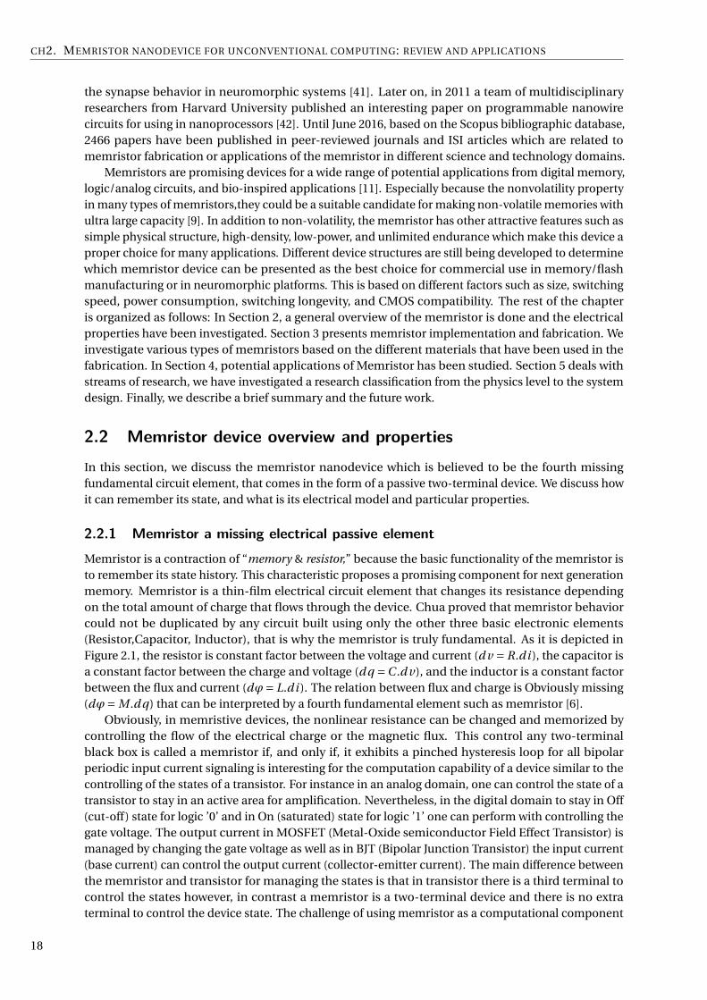
2.3 Memristor schematic and behavior: a) the memristor structure, the difference in applied voltage
changes doped and undoped regions, b) current versus voltage diagram, which demonstrates
hysteresis characteristic of a memristor, in the simulation we apply the sinusoidal input wave with an
amplitude of 1.5v, different frequencies, RON = 100Ω,ROF F = 15kΩ,D = 10nm,µv = 10−10cm2s−1V −1. 21
3
LIST OF FIGURES
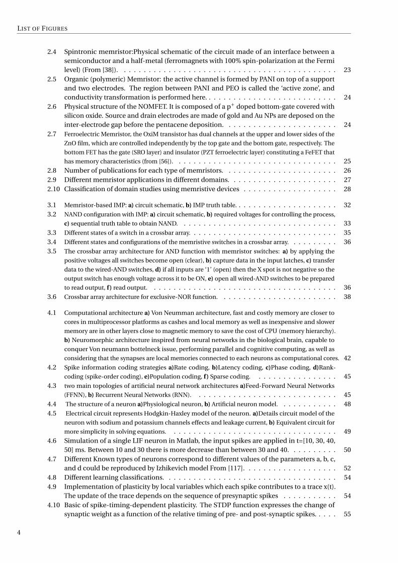
2.4 Spintronic memristor:Physical schematic of the circuit made of an interface between asemiconductor and a half-metal (ferromagnets with 100% spin-polarization at the Fermilevel) (From [38]). . . . . . . . . . . . . . . . . . . . . . . . . . . . . . . . . . . . . . . . . . . . 23
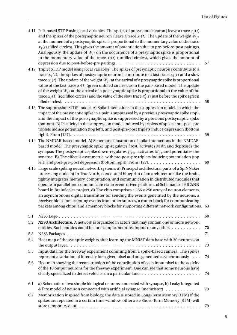
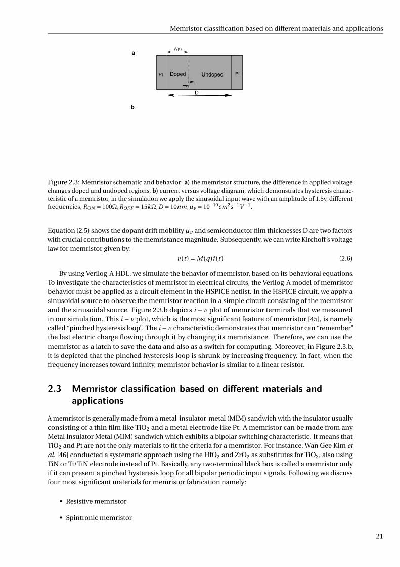
2.5 Organic (polymeric) Memristor: the active channel is formed by PANI on top of a supportand two electrodes. The region between PANI and PEO is called the ‘active zone’, andconductivity transformation is performed here. . . . . . . . . . . . . . . . . . . . . . . . . . . 24
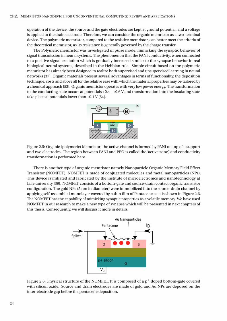
2.6 Physical structure of the NOMFET. It is composed of a p+ doped bottom-gate covered withsilicon oxide. Source and drain electrodes are made of gold and Au NPs are deposed on theinter-electrode gap before the pentacene deposition. . . . . . . . . . . . . . . . . . . . . . . 24
2.7 Ferroelectric Memristor, the OxiM transistor has dual channels at the upper and lower sides of the
ZnO film, which are controlled independently by the top gate and the bottom gate, respectively. The
bottom FET has the gate (SRO layer) and insulator (PZT ferroelectric layer) constituting a FeFET that
has memory characteristics (from [56]). . . . . . . . . . . . . . . . . . . . . . . . . . . . . . . . . 252.8 Number of publications for each type of memristors. . . . . . . . . . . . . . . . . . . . . . . 262.9 Different memristor applications in different domains. . . . . . . . . . . . . . . . . . . . . . 272.10 Classification of domain studies using memristive devices . . . . . . . . . . . . . . . . . . . 28
3.1 Memristor-based IMP: a) circuit schematic, b) IMP truth table. . . . . . . . . . . . . . . . . . . . . 323.2 NAND configuration with IMP: a) circuit schematic, b) required voltages for controlling the process,
c) sequential truth table to obtain NAND. . . . . . . . . . . . . . . . . . . . . . . . . . . . . . . . 333.3 Different states of a switch in a crossbar array. . . . . . . . . . . . . . . . . . . . . . . . . . . . . . 353.4 Different states and configurations of the memristive switches in a crossbar array. . . . . . . . . . 363.5 The crossbar array architecture for AND function with memristor switches: a) by applying the
positive voltages all switches become open (clear), b) capture data in the input latches, c) transfer
data to the wired-AND switches, d) if all inputs are ‘1’ (open) then the X spot is not negative so the
output switch has enough voltage across it to be ON, e) open all wired-AND switches to be prepared
to read output, f ) read output. . . . . . . . . . . . . . . . . . . . . . . . . . . . . . . . . . . . . . 363.6 Crossbar array architecture for exclusive-NOR function. . . . . . . . . . . . . . . . . . . . . . . . 38
4.1 Computational architecture a) Von Neumman architecture, fast and costly memory are closer to
cores in multiprocessor platforms as cashes and local memory as well as inexpensive and slower
memory are in other layers close to magnetic memory to save the cost of CPU (memory hierarchy).
b) Neuromorphic architecture inspired from neural networks in the biological brain, capable to
conquer Von neumann bottelneck issue, performing parallel and cognitive computing, as well as
considering that the synapses are local memories connected to each neurons as computational cores. 424.2 Spike information coding strategies a)Rate coding, b)Latency coding, c)Phase coding, d)Rank-
coding (spike-order coding), e)Population coding, f ) Sparse coding. . . . . . . . . . . . . . . . . 454.3 two main topologies of artificial neural network architectures a)Feed-Forward Neural Networks
(FFNN), b) Recurrent Neural Networks (RNN). . . . . . . . . . . . . . . . . . . . . . . . . . . . . 454.4 The structure of a neuron a)Physiological neuron, b) Artificial neuron model. . . . . . . . . . . . 484.5 Electrical circuit represents Hodgkin-Haxley model of the neuron. a)Details circuit model of the
neuron with sodium and potassium channels effects and leakage current, b) Equivalent circuit for
more simplicity in solving equations. . . . . . . . . . . . . . . . . . . . . . . . . . . . . . . . . . 494.6 Simulation of a single LIF neuron in Matlab, the input spikes are applied in t=[10, 30, 40,
50] ms. Between 10 and 30 there is more decrease than between 30 and 40. . . . . . . . . . 504.7 Different Known types of neurons correspond to different values of the parameters a, b, c,
and d could be reproduced by Izhikevich model From [117]. . . . . . . . . . . . . . . . . . . 524.8 Different learning classifications. . . . . . . . . . . . . . . . . . . . . . . . . . . . . . . . . . . 544.9 Implementation of plasticity by local variables which each spike contributes to a trace x(t).
The update of the trace depends on the sequence of presynaptic spikes . . . . . . . . . . . 544.10 Basic of spike-timing-dependent plasticity. The STDP function expresses the change of
synaptic weight as a function of the relative timing of pre- and post-synaptic spikes. . . . . 55
4
List of Figures
4.11 Pair-based STDP using local variables. The spikes of presynaptic neuron j leave a trace x j (t )and the spikes of the postsynaptic neuron i leave a trace xi (t ). The update of the weight W j i
at the moment of a postsynaptic spike is proportional to the momentary value of the tracex j (t ) (filled circles). This gives the amount of potentiation due to pre-before-post pairings.Analogously, the update of W j i on the occurrence of a presynaptic spike is proportionalto the momentary value of the trace xi (t) (unfilled circles), which gives the amount ofdepression due to post-before-pre pairings . . . . . . . . . . . . . . . . . . . . . . . . . . . . 57
4.12 Triplet STDP model using local variables. The spikes of presynaptic neuron j contribute to atrace x j (t), the spikes of postsynaptic neuron i contribute to a fast trace xi (t) and a slowtrace x ′
i (t ). The update of the weight W j i at the arrival of a presynaptic spike is proportionalvalue of the fast trace xi (t ) (green unfilled circles), as in the pair-based model. The updateof the weight W j i at the arrival of a postsynaptic spike is proportional to the value of thetrace x j (t ) (red filled circles) and the value of the slow trace x ′
i (t ) just before the spike (greenfilled circles). . . . . . . . . . . . . . . . . . . . . . . . . . . . . . . . . . . . . . . . . . . . . . . 58
4.13 The suppression STDP model. A) Spike interactions in the suppression model, in which theimpact of the presynaptic spike in a pair is suppressed by a previous presynaptic spike (top),and the impact of the postsynaptic spike is suppressed by a previous postsynaptic spike(bottom). B) Plasticity in the suppression model induced by triplets of spikes: pre-post-pretriplets induce potentiation (top left), and post-pre-post triplets induce depression (bottomright), From [127]. . . . . . . . . . . . . . . . . . . . . . . . . . . . . . . . . . . . . . . . . . . . 59
4.14 The NMDAR-based model. A) Schematic illustration of spike interactions in the NMDAR-based model. The presynaptic spike up-regulates f rest, activates M dn and depresses thesynapse. The postsynaptic spike down-regulates fr est , activates Mup and potentiates thesynapse. B) The effect is asymmetric, with pre-post-pre triplets inducing potentiation (topleft) and post-pre-post depression (bottom right), From [127]. . . . . . . . . . . . . . . . . . 60
4.15 Large scale spiking neural network systems, a) Principal architectural parts of a SpiNNakerprocessing node, b) In TrueNorth, conceptual blueprint of an architecture like the brain,tightly integrates memory, computation, and communication in distributed modules thatoperate in parallel and communicate via an event-driven platform. c) Schematic of HICANNboard in BrainScales project, d) The chip comprises a 256×256 array of neuron elements,an asynchronous digital transmitter for sending the events generated by the neurons, areceiver block for accepting events from other sources, a router block for communicatingpackets among chips, and a memory blocks for supporting different network configurations. 63
5.1 N2S3 Logo . . . . . . . . . . . . . . . . . . . . . . . . . . . . . . . . . . . . . . . . . . . . . . . . 68
5.2 N2S3 Architecture. A network is organized in actors that may contain one or more networkentities. Such entities could be for example, neurons, inputs or any other. . . . . . . . . . . 70
5.3 N2S3 Packages . . . . . . . . . . . . . . . . . . . . . . . . . . . . . . . . . . . . . . . . . . . . . 71
5.4 Heat map of the synaptic weights after learning the MNIST data base with 30 neurons onthe output layer. . . . . . . . . . . . . . . . . . . . . . . . . . . . . . . . . . . . . . . . . . . . . 73
5.5 Input data for the freeway experiment comming from a spike-based camera. The spikesrepresent a variation of intensity for a given pixel and are generated asynchronously. . . . 74
5.6 Heatmap showing the reconstruction of the contribution of each input pixel to the activityof the 10 output neurons for the freeway experiment. One can see that some neurons haveclearly specialized to detect vehicles on a particular lane. . . . . . . . . . . . . . . . . . . . . 74
6.1 a) Schematic of two simple biological neurons connected with synapse, b) Leaky Integrated& Fire model of neuron connected with artificial synapse (memristor) . . . . . . . . . . . . 79
6.2 Memorization inspired from biology, the data is stored in Long-Term Memory (LTM) if thespikes are repeated in a certain time-window, otherwise Short-Term Memory (STM) willstore temporary data. . . . . . . . . . . . . . . . . . . . . . . . . . . . . . . . . . . . . . . . . . 79
5
LIST OF FIGURES
6.3 Artificial synapse: a) Schematic view of the NOMFET as a volatile memory, b) TiO2 basednonvolatile memory, c) Synapse box schematic, d) Equivalent circuit with simple elements 81
6.4 Synaptic weights (conductance of non volatile memristor) learned in simulation using thesynapse box with 100 output neurons. The weights in the corners are random because theywere always filtered out by the volatile memristor and thus are never modified or even read. 82
6.5 Recognition rate as a function of number of output neurons. In the box plot for each numberof neuron, we compare the recognition rate of the two synapse models. The whiskers of thebox plot represent the minimum and maximum recognition rates of the 10 simulations. . 83
7.1 Neuromorphic vs SNN, a) The memristive synapse connects the spiking neurons in con-figurable crossbar array suitable for stdp unsupervised learning, the presynaptic neuronsare considered as inputs and postsynaptic neurons play output rolls. b) The spiking neuralnetwork two layers of this three layers could similarly operates as crossbar array. . . . . . 86
7.2 Sample heat maps of the synaptic weights after network training with four different numbersof output neurons (20, 30, 50 and 100). . . . . . . . . . . . . . . . . . . . . . . . . . . . . . . 87
7.3 The comparison of three different distributions for generating spike train by transferringMNIST database pixels to spike train. These distributions are tested with different numberof neurons=20, 30, 50, 100. . . . . . . . . . . . . . . . . . . . . . . . . . . . . . . . . . . . . . . 88
7.4 The recognition rate of the network using different number of neurons and three spike traindistributions. . . . . . . . . . . . . . . . . . . . . . . . . . . . . . . . . . . . . . . . . . . . . . . 90
7.5 The comparison of different STDP-window duration for using different number of neu-rons=20, 30, 50, 100. The MNIST digits dataset after converting to the corresponding spikesto the pixels densities, are presenting to the network for 350 ms for (each frame). The 150 mspause between each digit presenting are considered. This figure illustrates the performanceof neural network using four various number of neurons and different STDP-windows. . . 91
7.6 The recognition rate of the network using different number of neuron and six differentSTDP-wnidows. . . . . . . . . . . . . . . . . . . . . . . . . . . . . . . . . . . . . . . . . . . . . 92
7.7 The comparison of various threshold (15, 25, 35, 45 mV) for using different number ofneurons=20, 30, 50, 100. The threshold between 25 and 35 mV demonstrate better perfor-mance in the network, however, in the network with smaller number of neurons the neuronwith less threshold have still acceptable performance and on the contrary in larger neuralnetworks the neuron with more firing threshold voltage (such as 45 mV using for the 100output neurons) have demonstrated acceptable performance too. . . . . . . . . . . . . . . 93
7.8 comparing network performance using various number of neuron with different threshold 937.9 The comparison of various fitting parameters (β) for using different number of neurons=20,
30, 50, 100. The results demonstrate better performance using β between 1.8 and 2. How-ever, the differences are not distinguishable which is a prove of memristor devices robust-ness to the variations. . . . . . . . . . . . . . . . . . . . . . . . . . . . . . . . . . . . . . . . . . 94
7.10 comparing network performance using various number of neurons with different fittingparameter (β) for synapse model. . . . . . . . . . . . . . . . . . . . . . . . . . . . . . . . . . . 95
7.11 Using the best parameters significantly improves the recognition rate. . . . . . . . . . . . . 95
8.1 Restricted Boltzmann Machine is a network of neurons which neurons in one layer areconnected to all neurons in the next layer. . . . . . . . . . . . . . . . . . . . . . . . . . . . . . 98
8.2 Siegert abstract neuron model [184] . . . . . . . . . . . . . . . . . . . . . . . . . . . . . . . . 1008.3 Stacking RBMs as the main building blocks of DBN . . . . . . . . . . . . . . . . . . . . . . . 1018.4 Some sample images from ORL dataset . . . . . . . . . . . . . . . . . . . . . . . . . . . . . . 1018.5 The proposed DBN with Siegert neurons for learning ORL . . . . . . . . . . . . . . . . . . . 1028.6 Visualizing the learned features by hidden units . . . . . . . . . . . . . . . . . . . . . . . . . 1028.7 Accuracy of the proposed DBN with Siegert neurons in face recognition on ORL dataset . 1038.8 Decreasing the number of epochs and increasing the mini-batch size can reduce the model
accuracy . . . . . . . . . . . . . . . . . . . . . . . . . . . . . . . . . . . . . . . . . . . . . . . . 103
6

8.9 The upper row shows 10 of the training images and the lower one illustrate the correspond-ing reconstructed images . . . . . . . . . . . . . . . . . . . . . . . . . . . . . . . . . . . . . . . 104
8.10 The upper row shows 10 of the test images and the lower one illustrate the predicted images 104
List of Tables
2.1 Table of different class of memristors based on different materials and its applications, thefirst university/lab announcement of the device is listed too. . . . . . . . . . . . . . . . . . . 26
3.1 Different logic operations made by IMP operations and the number of required memristors . . . . 343.2 The number of memristive switches to make logic gates for the imp and crossbar array approaches. 38
6.1 Comparing network architecture efficiency for two synapses: nonvolatile (NV) v.s volatile-nonvolatile (VNV) synapse . . . . . . . . . . . . . . . . . . . . . . . . . . . . . . . . . . . . . . 83
7.1 Best parameters vs. baseline parameters . . . . . . . . . . . . . . . . . . . . . . . . . . . . . . 94
8.1 LIF parameters . . . . . . . . . . . . . . . . . . . . . . . . . . . . . . . . . . . . . . . . . . . . . 101
7

Chapter 1
Introduction
1.1 IntroductionThe two most important demands of humans using ICT devices and technologies are becoming twohottest topic of research in computer science and engineering namely Big Data and Internet of Things(IoT). In both domains, the way of processing data is quite important. In Big Data the clustering,classification, and prediction are not avoidable to use and process the data efficiently. In IoT, thesmart devices are connected to other smart devices using different sensors. Machine learning recentlyproposed promising solution for processing data in these two domains. By 2020, there will be 50 to100 billion devices connected to the Internet, ranging from smartphones, PCs, and ATMs (AutomatedTeller Machine) to manufacturing equipment in factories and products in shipping containers [1]. Forthe Big Data or sensory data not only an efficient processing algorithm is necessary but also finding anew fast, parallel and power-efficient hardware architecture is unavoidable.
Machine learning algorithms are widely used for data classification in software domain and usingconventional hardware platform. These algorithms on nowadays computers consume a remarkabletime and energy. The reason is that in conventional computing, the way of communicating betweenmemory and central processing unit (CPU) is not efficient. The memory wall or Von Neumann memorybottelneck is the growing disharmony of communication speed between the CPU and memory outsidethe CPU chip. An important reason for this disharmony is the restricted communication bandwidthbeyond chip boundaries, which is referred to as bandwidth wall as well. The CPUs access both dataand program in memory using the same shared resources. Finally, CPUs spend most of their time idle.
Using emerging technologies such as memristors [2], there is possibility of performing both infor-mation processing and storing the computational results on the same physical platform [3]. Memristorshave the potential to be a promising device for novel paradigms of computation as well as new genera-tion of memory. The characteristics of memristor are promising to design a processing unit with localaccess memory rather than non-local and shared memory. The new high performance architecturefor next generation of computation regarding to emerging technologies could be in logic or analogdomain. Memristors have potential for both digital and analog paradigms of computations.
Another novel alternative architecture suitable for neural network and machine learning algorithmsis proposed as Spiking Neural Network (SNN) system which is known as Neuromorphic architecturetoo. SNN is the known way to realize the neural network software abilities on a hardware architec-ture. The mammalian nervous system is a network of extreme complexity which is able to performcognitive computation in a parallel and power-efficient manner. Understanding the principles ofbrain processing for computational modeling is one of the biggest challenges of the 21st centurythat led to the new branch of research e.g., neuromorphic computing. Neuromorphic engineeringrepresents one of the promising fields for developing new computing paradigms complementing oreven replacing current Von Neumann architecture [4]. The requirements for implementing a SNNarchitecture (neuromorphic) are providing electronic devices that can mimic the biological neuralnetwork components such as neurons and synapses. The Spiking neural model is an electrical model of
9

CH1. INTRODUCTION
physiological neuron that has been implemented on the circuit using state-of-the-art technologies e.g.,CMOS transistors or on low-power CMOS design using subthreshold regime transistor [5]. The synapsein biological neural network reacts as a plastic connection controller between two neurons. Recently,emerging devices in nano-scale have demonstrated novel properties for making new memories andArtificial synapse. One of those is the memristor that was hypothetically presented by Leon Chua in1971 [6] and after a few decades, HP was the first to announce the successful memristor fabrication [2].The unique properties in memristor nano-devices such as, extreme scalability, flexibility because ofanalog behavior, and ability to remember the last state make the memristor a very promising candidateto apply it as a synapse in Spiking Neural Network (SNN) [7].
1.2 Part I:Motivation, state-of-the-art and application of usingemerging nanodevices for unconventional computing
The first part of this dissertation contains the mathematic and physical model of memristor, memristivenanodevice technologies, as well as different applications of this emerging technology. Memristorcan remember its last state after the last power plugging and has a simple physical structure, high-density integration, and low-power consumption. These features make the memristor an attractivecandidate for building the next generation of memories [8–10], an artificial synapse in Spiking NeuralNetwork architectures [7, 11], and as a switch in crossbar array configurations [12]. Different devicestructures are still being developed to determine which memristor device can be presented as thebest choice for commercial use in memory/flash manufacturing or in neuromorphic platforms. Thisis based on different factors such as size, switching speed, power consumption, switching longevity,and CMOS compatibility. A comprehensive survey particularly on recent research results and recentdevelopment of memristive devices seems be quite useful for future research work and developments.To better understanding how memristor can restore the data and how it could be flexible to modify theconductances to be replaced as a synapse, we have modeled the behavior of this device. In addition, weperform a classification of the devices based on the manufacturing technology. In this classification, wediscuss different characteristics of various devices. We study the potential applications of a memristorbuilt using specific technology. The advantages and disadvantages of each class of memristor withvarious type of device materials are discussed. Furthermore, we discuss potential applications ofmemristor nanodevice in nonvolatile memories such as RRAM, PCM, CBRAM, FeRAM and MRAM,digital computation, analog and neuromorphic domains.
In the second chapter, we discuss two methods for unconventional digital computing by memristivetwo-terminal devices [13]. Two main digital computation approaches, namely material implication(IMP) or stateful logic [14, 15] and programmable crossbar architecture [16, 17] are studied in thischapter. By applying memristor as a digital switch, a high memristance (memristor resistance) isconsidered as logic ‘0’ and a low memristance is considered as logic ‘1’. First and foremost, based onthe previous research works on IMP, we establish a functionally complete Boolean operation to be ableto build all standard logic gates. Subsequently, building the digital gates has been performed usingprogrammable crossbar architectures. Programmable crossbar architectures have been proposed as apromising approach for future computing architectures because of their simplicity of fabrication andhigh density, which support defect tolerance. At the end of Chapter 3, the comparison of two methodsin digital computation is presented.
In the last chapter of part I, the basic definition of neuromorphic or Spiking Neural Network(SNN) architecture have been introduced. Neuromorphic computing has the potential to bring verylow power computation to future computer architectures and embedded systems [18]. The mainremarkable difference between conventional Von Neumann architecture and neuromorphic systemsis in their use of memory structures. The way of communication between memory and centralprocessing unit (CPU) in conventional computing is not very efficient which is known as Von Neumannmemory bottelneck. CPUs spend most of their time idle because the speed difference between theCPU and memory. The solution that has been applied in Von Neumann architecture is memory
10

Part II:Our contribution in spiking neural network architecture: Simulator, New synapse box, Parameterexploration and Spiking deep learning
hierarchy. In other words, a limited amount of fast but costly memory sit closer to the processingunit, while most of the data is stored in a cheaper but larger memory. By proposing computing unitnext to the local memory, neuromorphic brain-inspired computing paradigms offer an attractivesolution for implementing alternative non von Neumann architectures, using advanced and emergingtechnologies [4,19]. Artificial neural network (ANN) is a mathematical model of the network of neuronsin mammalian brain though SNN is an electronic hardware neuromorphic model of biological brain.SNNs provide powerful tools to emulate data processing in the brain, including neural informationprocessing, plasticity and learning. Consequently, spiking networks offer solutions to a broad rangeof specific problems in applied engineering image detection, event detection, classification, speechrecognition and many cognitive computation domain applications.
Neurons communicate together using spikes. In Chapter 4, we review different ways of codingdata to spikes known as spike information coding methods. Furthermore, we study the networktopologies and configurations. The interconnection among units can be structured in numerousways resulting in numerous possible topologies. Two basic classes are defined: Feed-Forward NeuralNetworks (FFNN) and Recurrent (or feedback) Neural Networks (RNN) depicted in Figure 4.3. We adda discussion in more modern neural networks such as Convolutional Neural Networks (CNN) [20], andDeep Belief Networks (DBNs) [21]. Moreover, various spiking model of neurons as dynamic elementsand processing units are reviewed. We discuss which model we have used in our platform and whywe choose this model. Thanks to the plasticity property of synapse, in neural network system, wecan basically say the synapse is where the learning happens. Therefore, in this chapter both synapseand learning are studied. Additionally, we discussed various classes of learning algorithms as wellas a comprehensive study of Spike-Timing Dependent Plasticity (STDP) [22, 23] is presented. Thiscomprehensive study includes presenting different models for STDP learning based on single ormultiple pre- or postsynaptic spikes occurring across a synapse in an interval of time. Finally inChapter 4, we applied lateral inhibition which is winner-take-all (WTA) [24, 25] in our platform as wellas homeostasis as a method of neuron adaptation of learning.
1.3 Part II:Our contribution in spiking neural network architecture:Simulator, New synapse box, Parameter exploration andSpiking deep learning
The second part of the thesis consists of our contributions to neuromorphic computing and SNN archi-tecture. In Chapter 5, we present and develop N2S3 (for Neural Network Scalable Spiking Simulator), anopen-source event-driven simulator that is built to help design spiking neuromorphic circuits based onnanoelectronics. It is dedicated to intermediate modeling level, between low-level hardware descrip-tion languages and high-level neural network simulators used primarily in neurosciences as well as theintegration of synaptic memristive device modeling, hardware constraints and any custom featuresrequired for the target application. N2S3 has been developed from the ground up for extensibility,allowing to model various kinds of neurons and synapses, network topologies, learning procedures,reporting facilities, and to be user-friendly, with a domain specific language to easily express andrun new experiments. For experimental set up, N2S3 is distributed with the implementation of two“classical” experiments: handwritten digit recognition on the MNIST dataset [20, 26] and the highwayvehicle counting experiment [27].
In Chapter 6, with the combination of a volatile and a nonvolatile memristor we introduce anddesign a new artificial synapse box that can improve learning in spiking neural networks architectures[28]. This novel synapse box is able to forget and remember by inspiration from biological synapses.The nonvolatility is a unique property in memristor nanodevice to introduce it as a promising candidatein building next generation of non-volatile memory. However, by inspiring of physiological synapse,a synapse that can forget unimportant data (non-frequent spikes) and remember significant data(frequent spike trains) can support network to improve learning process.
11

CH1. INTRODUCTION
Thanks to close collaboration with the nano-electronics research center in the University of Lille(IEMN), we have had the opportunity of studying the suitability of different types of memristors (TiO2 ,NOMFET, magnetoresistive, magnetoelectric) to build a spiking neural network hardware platform. Toadd the forgetting property to the synapse box, we have used a volatile memristor named NOMFET(Nanoparticle Organic Memory Field-Effect Transistor). We have merged NOMFET with a nonvolatilesolid-state meristor nanodevice. At the end of this chapter, we evaluate the synapse box proposal bycomparing it with a single non-volatile memory synapse by simulation on the MNIST handwrittendigit recognition benchmark.
Specific application domains such as Big Data classification, visual processing, pattern recognitionand in general sensory input data, require information processing systems which are able to classifythe data and to learn from the patterns in the data. Such systems should be power-efficient. Thusresearchers have developed brain- inspired architectures such as spiking neural networks. In Chap-ter 7, we surveyed brain- inspired architectures approaches with studying well-known project andarchitecture in this neuromorphic domain. For large scale brain-like computing on neuromorphichardware we have recognized four approaches:
• Microprocessor based approaches where the system can read the codes to execute and modelthe behavior of neural systems and cognitive computation such as the SpiNNaker machine [29].
• Fully digital custom circuits where the neural system components are modeled in circuit usingsate-of-the-art CMOS technology e.g., IBM TrueNorth machine [18].
• Analog/digital mixed-signal systems that model the behavior of biological neural systems, e.g.the NeuroGrid [30] and BrainScales [31] projects.
• Memristor crossbar array based systems where the analog behavior of the memristors emulatethe synapses of a spiking neural network [32].
We have studied large scale brain-like architectures such as SpiNNaker, IBM TrueNorth, NeuroGrid,and BrainScales to recognize the cons and pros of these projects to have our optimized evaluation andexploration of required items and parameters for neuromorphic and brain-like computation platforms.
Spiking neural networks are widely used in the community of computational neuroscience andneuromorphic computation, there is still a need for research on the methods to choose the opti-mum parameters for better recognition efficiency. Our main contribution in Chapter 7 is to evaluateand explore the impact of several parameters on the learning performance of SNNs for the MNISTbenchmark: the number of neurons in the output layer, the duration of the STDP window, variousthresholds for adaptive threshold neurons, different distributions of spikes to code the input imagesand the memristive synapse fitting parameter. This evaluation has shown that a careful choice of a fewparameters can significantly improve the recognition rate on this benchmark.
Deep learning is currently a very active research area in machine learning and pattern recognitionsociety due to its potential to classify and predict as a result of processing Big data and Internet of Things(IoT) related data. Deep Learning is a set of powerful machine learning methods for training deeparchitectures. Considering the inherent inefficiency of learning methods from traditional ArtificialNeural Networks in deep architectures, Contrastive Divergence (CD) has been proposed to trainRestricted Boltzmann Machines (RBM) as the main building blocks of deep networks [33].
In Chapter 8 deep learning architectures are introduced in SNN systems. In SNN, neurons com-municate using spikes [34]. Therefore, we have to design an architecture of neurons that are able toimplement spiking data. Consequently, we present a framework for using Contrastive Divergence totrain an SNN using RBM and spiking neurons. The obtained recognition rate or network accuracy ofthe architecture using CD algorithms for learning was 92.4%. This framework can open a new windowtoward the neruromorphic architecture designer to apply the state-of-the-art of machine learninglearning algorithm in SNN architecture.
12

Manuscript outline
CH1.Introduction
Part I. Usingnanodvices forunconventionalcomputing
Part II. Ourcontributionin spiking
neural networkarchitecture
Ch2. Memristornew emerging de-vice:review and appli-cations
Ch3. Unconven-tional digital com-puting using memris-tors
Ch4. Neuromorphiccomputing in Spik-ing Neural NetworkArchitecture
Ch5. N2S3, scal-able neuromorphichardware simulator
Ch6. Combining aVolatile and Non-volatile Memristor insynapse box
Ch7. Evaluation andparameter explo-ration in SNN
Ch8. Deep learningin spiking neuralnetwork
Figure 1.1: General overview of the manuscript.
1.4 Manuscript outlineThis manuscript presents a spiking neural network platform suitable to hardware implementationwith a focus on learning in SNN. Therefore in the first two chapters, we review cons and pros ofmemristor and memristive-based computation. The different models and technologies of memristorbeside the applications is presented in chapter 2. The third chapter consists of using memristors inthe unconventional digital manner. In the chapter 4, the principals of neuromorphic and spikingneural network architecture is described. Our contribution in designing and presenting spiking neuralnetwork architecture is presented in the second part of this manuscript. First of all, in the contributionpart we present our neuromorphic hardware simulator. Second, we propose an artificial synapse boxto improve learning by combining volatile and nonvolatile types of memristor devices. Furthermore,in Chapter 7, we discuss different parameters in SNN architecture and evaluate the effect of eachparameters in learning. In Chapter 8, deep learning in spiking neural network is presented. Finally theconclusion and potential future work are explained. A general overview of this dissertation is shown inFigure 1.1.
13


Part I
Motivation, state-of-the-art andapplication of using emerging nanodevices
for unconventional computing
15


Chapter 2
Memristor nanodevice forunconventional computing: review and
applications
Abstract
A memristor is a two-terminal nanodevice. Its properties attract a wide community of re-searchers from various domains such as physics, chemistry, electronics, computer and neuro-science. The simple structure for manufacturing, small scalability, nonvolatility and potentialof using in low power platforms are outstanding characteristics of this emerging technology. Inthis chapter, we review a brief literature of memristor from mathematic model to the physicalrealization and different applications. We discuss different classes of memristors based on thematerial used for its manufacturing. The potential applications of memristor are presented and awide domain of applications are classified.
2.1 IntroductionMemristor has recently drawn the wide attention of scientists and researchers due to non-volatility,better alignment, and excellent scalability properties [35]. Memristor has initiated a novel researchdirection for the advancement of neuromorphic and neuro-inspired computing. Memristor remembersits last state after the last power plugging and has a simple physical structure, high-density integration,and low-power consumption. These features make the memristor an attractive candidate for buildingthe next generation of memories [8]. In addition, from high-performance computing point of view,the memristor has the potential capability to conquer the memory bottleneck issue, by utilizingcomputational unit next to the memory [3]. Due to these unique properties and potentials of thememristor, neuroscientists and neuromorphic researchers apply it as an artificial synapse in SpikingNeural Network (SNN) architectures [7].
Memristor was predicted in 1971 by Leon Chua, a professor of electrical engineering at the Uni-versity of California, Berkeley, as the fourth fundamental device [6]. Publishing a paper in the Naturejournal by Hewlett Packard (HP) [2] in May 2008, announced the first ever experimental realizationof the memristor, caused an extraordinary increased interest in this passive element. Based on thesymmetry of the equations that govern the resistor, capacitor, and inductor, Chua hypothesized thatfourth device should exist that holds a relationship between magnetic flux and charge. After the physi-cal discovery of the memristor, several institutions have published the memristor device fabricationsusing a variety of different materials and device structures [2, 36–39].
In 2009, Biolek et al. modeled nonlinear dopant drift memristor by SPICE [40]. One year later, WeiLu, professor at the University of Michigan proposed a nanoscale memristor device which can mimic
17
CH2. MEMRISTOR NANODEVICE FOR UNCONVENTIONAL COMPUTING: REVIEW AND APPLICATIONS
the synapse behavior in neuromorphic systems [41]. Later on, in 2011 a team of multidisciplinaryresearchers from Harvard University published an interesting paper on programmable nanowirecircuits for using in nanoprocessors [42]. Until June 2016, based on the Scopus bibliographic database,2466 papers have been published in peer-reviewed journals and ISI articles which are related tomemristor fabrication or applications of the memristor in different science and technology domains.
Memristors are promising devices for a wide range of potential applications from digital memory,logic/analog circuits, and bio-inspired applications [11]. Especially because the nonvolatility propertyin many types of memristors,they could be a suitable candidate for making non-volatile memories withultra large capacity [9]. In addition to non-volatility, the memristor has other attractive features such assimple physical structure, high-density, low-power, and unlimited endurance which make this device aproper choice for many applications. Different device structures are still being developed to determinewhich memristor device can be presented as the best choice for commercial use in memory/flashmanufacturing or in neuromorphic platforms. This is based on different factors such as size, switchingspeed, power consumption, switching longevity, and CMOS compatibility. The rest of the chapteris organized as follows: In Section 2, a general overview of the memristor is done and the electricalproperties have been investigated. Section 3 presents memristor implementation and fabrication. Weinvestigate various types of memristors based on the different materials that have been used in thefabrication. In Section 4, potential applications of Memristor has been studied. Section 5 deals withstreams of research, we have investigated a research classification from the physics level to the systemdesign. Finally, we describe a brief summary and the future work.
2.2 Memristor device overview and propertiesIn this section, we discuss the memristor nanodevice which is believed to be the fourth missingfundamental circuit element, that comes in the form of a passive two-terminal device. We discuss howit can remember its state, and what is its electrical model and particular properties.
2.2.1 Memristor a missing electrical passive elementMemristor is a contraction of “memory & resistor,” because the basic functionality of the memristor isto remember its state history. This characteristic proposes a promising component for next generationmemory. Memristor is a thin-film electrical circuit element that changes its resistance dependingon the total amount of charge that flows through the device. Chua proved that memristor behaviorcould not be duplicated by any circuit built using only the other three basic electronic elements(Resistor,Capacitor, Inductor), that is why the memristor is truly fundamental. As it is depicted inFigure 2.1, the resistor is constant factor between the voltage and current (d v = R.di ), the capacitor isa constant factor between the charge and voltage (d q =C .d v), and the inductor is a constant factorbetween the flux and current (dϕ= L.di ). The relation between flux and charge is Obviously missing(dϕ= M .d q) that can be interpreted by a fourth fundamental element such as memristor [6].
Obviously, in memristive devices, the nonlinear resistance can be changed and memorized bycontrolling the flow of the electrical charge or the magnetic flux. This control any two-terminalblack box is called a memristor if, and only if, it exhibits a pinched hysteresis loop for all bipolarperiodic input current signaling is interesting for the computation capability of a device similar to thecontrolling of the states of a transistor. For instance in an analog domain, one can control the state of atransistor to stay in an active area for amplification. Nevertheless, in the digital domain to stay in Off(cut-off) state for logic ’0’ and in On (saturated) state for logic ’1’ one can perform with controlling thegate voltage. The output current in MOSFET (Metal-Oxide semiconductor Field Effect Transistor) ismanaged by changing the gate voltage as well as in BJT (Bipolar Junction Transistor) the input current(base current) can control the output current (collector-emitter current). The main difference betweenthe memristor and transistor for managing the states is that in transistor there is a third terminal tocontrol the states however, in contrast a memristor is a two-terminal device and there is no extraterminal to control the device state. The challenge of using memristor as a computational component
18

Memristor device overview and properties
Figure 2.1: Relations between the passive devices and the anticipating the place of the fourth funda-mental element based on the relations between charge (q) and flux (ϕ) (from [2]).
instead of transistor lies in the ability to control the working states as accurate as possible. Indeed, ina memristor both potentials for analog and digital computing have been presented. Consequently,using memristor in digital computing to make gate library or crossbar architecture as well as usingmemristor in analog domain (neuro-inspired or traditional) for computation are introduced in severalwork [3, 14–16, 43]. In next sections, we discuss different possibilities and our contributions to applymemristor in both digital and analog platforms.
2.2.2 Memristive device functionality
When you turn off the voltage, the memristor remembers its most recent resistance until the nexttime you turn it on, whether that happens a day later or a year later. It is worth mentioning that theduration to store the data in resistive form is dependent of the nano-device material. In other words,the volatility is different depending on the device materials in fabrication.
To understand the functionality of a memristor, let us imagine a resistor as a pipe which waterflows through it. The water simulates the electric charge. The resistor obstruction of the flow of chargeis comparable to the diameter of the pipe: the narrower the pipe, the greater the resistance. For thehistory of circuit design, resistors have had a fixed pipe diameter. But a memristor is a pipe that itsdiameter changes with the amount and direction of the water flows through it. If water flows throughthis pipe in one direction, it expands the pipe diameter (more conductive). But if the water flows in theopposite direction and the pipe shrinks (less conductive). Furthermore, let us imagine while we turnoff the flow, the diameter of the pipe freezes until the water is turned back on. It mimics the memristorcharacteristic to remember last state. This freezing property suits memristors brilliantly for the newgeneration of memory. The ability to indefinitely store resistance values means that a memristor canbe used as a nonvolatile memory.
Chua demonstrated mathematically that his hypothetical device would provide a relationshipbetween flux and charge similar to what a resistor provides between voltage and current. There wasno obvious physical interaction between charge and the integral over the voltage before HP discovery.Stanley Williams in [44] explained how they found the missing memristor and what is the relationbetween what they found and Chua mathematic model. In Figure 2.2, the oxygen deficiencies in theTiO2−x manifest as bubbles of oxygen vacancies scattered throughout the upper layer. A positive voltageon the switch repels the (positive) oxygen deficiencies in the metallic upper TiO2−x layer, sending theminto the insulating TiO2 layer below. That causes the boundary between the two materials to movedown, increasing the percentage of conducting TiO2−x and thus the conductivity of the entire switch.
19

CH2. MEMRISTOR NANODEVICE FOR UNCONVENTIONAL COMPUTING: REVIEW AND APPLICATIONS
Therefore, the more positive voltage causes the more conductivity in the cube. A negative voltage on
Figure 2.2: A material model of the memristor schematic to demonstrate TiO2 memristor functionality,positive charge makes the device more conductive and negative charge makes it less conductive.
the switch attracts the positively charged oxygen bubbles, pulling them out of the TiO2. The amount ofinsulating of resistive TiO2 increases, thereby making the switch more resistive. The more negativevoltage causes the less conductivity in the cube. What makes this switch a special device? When thevoltage across the device is turned off–positive or negative–the oxygen bubbles do not migrate. Theywill freeze where they have been before, which means that the boundary between the two titaniumdioxide layers is frozen. That is how the Memristor “remembers” the last state of conductivity as wellas it proves the plasticity properties in memristor to be applied as a synapse in an artificial neuralnetwork architecture and neuromorphic platform.
2.2.3 Electrical model
When an electric field is applied to the terminals of the memristor, the shifting in the boundary betweenits doped and undoped regions leads to variable total resistance of the device. In Figure 2.3.a, theelectrical behavior of memristor can be modeled as follows [2]:
v(t ) = Rmemi (t ) (2.1)
Rmem = RONw(t )
D+ROF F (1− w(t )
D) (2.2)
where w(t ) is the width of the doped region, D is the overall thickness of the TiO2 bi-layer, RON is theresistance when the active region is completely doped (w = D) and ROF F is the resistance, when theTiO2 bi-layer is mostly undopped (w→ 0).
d w(t )
d t=µv
RON
Di (t ) (2.3)
which yields the following formula for w(t ):
w(t ) =µvRON
Dq(t ) (2.4)
Where µv is the average dopant mobility. By inserting Equation (2.4) into Equation (2.2) and then intoEquation (2.1) we obtain the memristance of the device, which for RON «ROF F simplifies to:
Rmem = M(q) = ROF F (1− µv RON
D2 q(t )) (2.5)
20
Memristor classification based on different materials and applications
Pt Pt
D
W(t)
Doped Undoped
a
b
Figure 2.3: Memristor schematic and behavior: a) the memristor structure, the difference in applied voltagechanges doped and undoped regions, b) current versus voltage diagram, which demonstrates hysteresis charac-teristic of a memristor, in the simulation we apply the sinusoidal input wave with an amplitude of 1.5v, differentfrequencies, RON = 100Ω,ROF F = 15kΩ,D = 10nm,µv = 10−10cm2s−1V −1.
Equation (2.5) shows the dopant drift mobilityµv and semiconductor film thicknesses D are two factorswith crucial contributions to the memristance magnitude. Subsequently, we can write Kirchoff’s voltagelaw for memristor given by:
v(t ) = M(q)i (t ) (2.6)
By using Verilog-A HDL, we simulate the behavior of memristor, based on its behavioral equations.To investigate the characteristics of memristor in electrical circuits, the Verilog-A model of memristorbehavior must be applied as a circuit element in the HSPICE netlist. In the HSPICE circuit, we apply asinusoidal source to observe the memristor reaction in a simple circuit consisting of the memristorand the sinusoidal source. Figure 2.3.b depicts i − v plot of memristor terminals that we measuredin our simulation. This i − v plot, which is the most significant feature of memristor [45], is namelycalled “pinched hysteresis loop”. The i −v characteristic demonstrates that memristor can “remember”the last electric charge flowing through it by changing its memristance. Therefore, we can use thememristor as a latch to save the data and also as a switch for computing. Moreover, in Figure 2.3.b,it is depicted that the pinched hysteresis loop is shrunk by increasing frequency. In fact, when thefrequency increases toward infinity, memristor behavior is similar to a linear resistor.
2.3 Memristor classification based on different materials andapplications
A memristor is generally made from a metal-insulator-metal (MIM) sandwich with the insulator usuallyconsisting of a thin film like TiO2 and a metal electrode like Pt. A memristor can be made from anyMetal Insulator Metal (MIM) sandwich which exhibits a bipolar switching characteristic. It means thatTiO2 and Pt are not the only materials to fit the criteria for a memristor. For instance, Wan Gee Kim etal. [46] conducted a systematic approach using the HfO2 and ZrO2 as substitutes for TiO2, also usingTiN or Ti/TiN electrode instead of Pt. Basically, any two-terminal black box is called a memristor onlyif it can present a pinched hysteresis loop for all bipolar periodic input signals. Following we discussfour most significant materials for memristor fabrication namely:
• Resistive memristor
• Spintronic memristor
21

CH2. MEMRISTOR NANODEVICE FOR UNCONVENTIONAL COMPUTING: REVIEW AND APPLICATIONS
• Organic (Polymeric) memristor
• Ferroelectric memristor
2.3.1 Resistive MemristorBefore the memristor getting well-known, resistive materials have already been widely used in theresistive random access memories (ReRAM/RRAM) [47]. The storage function of ReRAM is realized byan intrinsic physical behavior in ReRAM, that is called resistive switching. The resistive material canbe switched between a high resistance state (HRS) and a low resistance state (LRS) under an externalelectrical input signal. The TiO2 memristor is a ReRAM fabricated in nanometre scale (2-3 nm) thinfilm that is depicted in Figure 2.3.a , containing a doped region and an undoped region. Strukov etal. [2] exploit a very thin-film TiO2 sandwiched between two platinum (Pt) contacts and one side ofthe TiO2 is doped with oxygen vacancies, which are positively charged ions. Therefore, there is a TiO2
junction where one side is doped and the other is undoped. Such a doping process results in twodifferent resistances: one is a high resistance (undoped) and the other is a low resistance (doped).The application of an external bias v(t) across the device will move the boundary between the tworegions by causing the charged dopants to drift. How TiO2 could change and store the state has beenintroduced in 2.2.2.
The obvious disadvantage of the first published TiO2 memristor was its switching speed (operateat only 1Hz). The switching speed was not comparable with SRAM, DRAM and even flash memory.Flash exhibit writing times of the order of a microsecond and volatile memories have writing speedsof the order of hundreds of picoseconds. Many research groups in different labs published theirfabrication results to demonstrate a faster switching speed device. In October 2011, HP lab developeda memristor switch using a SET pulse with a duration of 105 ps and a RESET pulse with a durationof 120 ps. The associated energies for ON and OFF switching were computed to be 1.9 and 5.8 pJ,respectively which are quite efficient for power-aware computations. The full-length D (Figure 2.3.a)of the TiO2 memristor is 10 nm [48] that proposes high-density devices in a small area in VLSI.
A research team at the University of Michigan led by Wei Lu [41] demonstrated another type ofresistive memristor that can be used to build brain- like computers and known as amorphous siliconmemristor. The Amorphous silicon memristor consists of a layered device structure including a co-sputtered Ag and Si active layer with a properly designed Ag/Si mixture ratio gradient that leads tothe formation of a Ag-rich (high conductivity) region and a Ag-poor (low conductivity) region. Thisdemonstration provides the direct experimental support for the recently proposed memristor-basedneuromorphic systems.
Amorphous silicon memristor can be fabricated with a CMOS compatible simple fabricationprocess using only common materials which is a great advantage of using amorphous silicon devices.The endurance test results of two extreme cases with programming current levels 10n A and 10m A are106 and 105 cycles respectively. We note the larger than 106 cycles of endurance with low programmingcurrents are already comparable to conventional flash memory devices. Wei Lu team have routinelyobserved switching speed faster than 5ns from the devices with a few mA on-current. The switching inthis device is faster than 5 ns with a few mA on-current that make it a promising candidate for high-speed switching applications. However, before the devices can be used as a switch, they need to gothrough a high voltage forming process (typically ≥ 10 V) which significantly reduces the performanceof power efficiency of devices [49]. Moreover, the retention time (data storage period) is still short (afew months).
2.3.2 Spintronic MemristorSpintronic memristor changes its resistance by varying the direction of the spin of the electrons.Magnetic Tunneling Junction (MTJ) has been used in commercial recording heads to sense magneticflux. It is the core device cell for spin torque magnetic random access memory and has also beenproposed for logic devices. In a spintronic device, the electron spin changes the magnetization state
22

Memristor classification based on different materials and applications
Figure 2.4: Spintronic memristor:Physical schematic of the circuit made of an interface betweena semiconductor and a half-metal (ferromagnets with 100% spin-polarization at the Fermi level)(From [38]).
of the device. The magnetization state of the device is thus dependent upon the cumulative effectsof electron spin excitations [50]. MTJ can be switched between a LRS and an HRS using the spin-polarized current induced between two ferromagnetic layers. If the resistance of this spintronic deviceis determined by its magnetization state, we could have a spintronic memristor with its resistancedepending upon the integral effects of its current profile.
The use of a fundamentally different degree of freedom which allows for the realization of memris-tive behavior is thus desirabled by Pershin and Di Ventra [38]. They demonstrated that the degree offreedom is provided by the electron spin and memristive behavior is obtained from the broad class ofsemiconductor spintronic devices. This class involves systems whose transport properties depend onthe level of electron spin polarization in a semiconductor which is influenced by an external controlparameter (such as an applied voltage). Pershin and Di Ventra considered a junction with half-metalsshown in Figure 2.4 (ferromagnets with 100% spin-polarization at the Fermi level), because thesejunctions react as perfect spin-filters, therefore they are more sensitive to the level of electron spinpolarization. They observed memristor behavior in the i − v curve of these systems. This means theproposed device is controllable and tunable. Furthermore, the device can be easily integrated on topof the CMOS. The integration of the spin torque memristor on CMOS is the same as the integration ofmagnetic random access memory cell on CMOS [51]. This has been achieved and commercialized inmagnetic random access memory.
The potential applications of spintronic memristor are in multibit data storage and logic, novelsensing scheme, low power consumption computing, and information security. However, the smallresistance ON/OFF ratio remains a notable concern for spintronic memristor devices.
2.3.3 Organic (Polymeric) Memristor
In 2005 Erokhin et al. [52] at the university of Parma reported a polymeric electrochemical element forthe adaptive networks. Even though it was not called a memristor, however mainly its characteristicscorresponds to the hypothetical memristor. At the heart of this device, there is a conducting channel,a thin polyaniline (PANI) layer, deposited onto an insulating support with two electrodes. A narrowstripe of solid electrolyte doped Poly Ethylene Oxide (PEO) which is formed in the central part of thechannel and used for the redox reactions. The area of PANI under PEO is the active zone (see Figure2.5). A thin silver wire is inserted into the solid electrolyte to provide the reference potential; such awire is connected to one of the electrodes on the solid support, kept at the ground potential level.
Conductivity variations and memory properties of the organic memristor are due to the redoxreactions occurring in the active zone, where PANI is reversibly transferred from the reduced insulatingstate into the oxidized conducting one [37]. In analogy with the nomenclature used in Field EffectTransistors (FETs), the two electrodes that are connected with the PANI film are called the sourceand drain electrodes, while the wire immersed in the PEO is called the gate electrode. In the normal
23
CH2. MEMRISTOR NANODEVICE FOR UNCONVENTIONAL COMPUTING: REVIEW AND APPLICATIONS
operation of the device, the source and the gate electrodes are kept at ground potential, and a voltageis applied to the drain electrode. Therefore, we can consider the organic memristor as a two-terminaldevice. The polymeric memristor, compared to the resistive memristor, can better meet the criteria ofthe theoretical memristor, as its resistance is generally governed by the charge transfer.
The Polymeric memristor was investigated in pulse mode, mimicking the synaptic behavior ofsignal transmission in neural systems. The phenomenon that the PANI conductivity, when connectedto a positive signal excitation which is gradually increased similar to the synapse behavior in realbiological neural systems, described in the Hebbian rule. Simple circuit based on the polymericmemristor has already been designed to realize both supervised and unsupervised learning in neuralnetworks [37]. Organic materials present several advantages in terms of functionality, the depositiontechnique, costs and above all for the relative ease with which the material properties may be tailored bya chemical approach [53]. Organic memristor operates with very low power energy. The transformationto the conducting state occurs at potentials +0.4 - +0.6 V and transformation into the insulating statetake place at potentials lower than +0.1 V [54].
Figure 2.5: Organic (polymeric) Memristor: the active channel is formed by PANI on top of a supportand two electrodes. The region between PANI and PEO is called the ‘active zone’, and conductivitytransformation is performed here.
There is another type of organic memristor namely Nanoparticle Organic Memory Field EffectTransistor (NOMFET). NOMFET is made of conjugated molecules and metal nanoparticles (NPs).This device is initiated and fabricated by the institute of microelectronics and nanotechnology atLille university [39]. NOMFET consists of a bottom-gate and source-drain contact organic transistorconfiguration. The gold NPs (5 nm in diameter) were immobilized into the source-drain channel byapplying self-assembled monolayer covered by a thin film of Pentacene as it is shown in Figure 2.6.The NOMFET has the capability of mimicking synaptic properties as a volatile memory. We have usedNOMFET in our research to make a new type of synapse which will be presented in next chapters ofthis thesis. Consequently, we will discuss it more in details.
ID
VG
Spikes
Pentacene
Au Nanoparticles
p+ silicon
D S
G
Figure 2.6: Physical structure of the NOMFET. It is composed of a p+ doped bottom-gate coveredwith silicon oxide. Source and drain electrodes are made of gold and Au NPs are deposed on theinter-electrode gap before the pentacene deposition.
24

Memristor classification based on different materials and applications
2.3.4 Ferroelectric MemristorFerroelectricity is a property of certain materials which have a spontaneous electric polarization thatcan be reversed by the application of an external electric field. The ferroelectric memristor is based ona thin ferroelectric barrier sandwiched between two metallic electrodes. Therefore, these two oppositepolarization states can be used to represent binary bits ‘0’ and ‘1’, thus resulting in the advent of theFerroelectric Random Access Memory (FeRAM). Due to FeRAM nonvolatility, ferroelectric materialshave been widely used in automobile equipment, ID/smart card, Radio Frequency Identification(RFID) and other embedded memory applications [55].
Chanthbouala, A. et al. [36], showed voltage-controlled domain configurations in ferroelectrictunnel barriers yield memristive behavior with resistance variations exceeding two orders of magnitudeand a 10 ns operation speed. They reported Piezoresponse Force Microscopy (PFM) images andelectrical transport measurements as a function of the amplitude, duration and the repetition numberof voltage pulses in the 10-200 ns range. In tunnel junctions with a ferroelectric barrier, switching theferroelectric polarization induces variations of the tunnel resistance, with resistance contrasts betweenthe ON and OFF states of several orders of magnitude. The low-resistance state (RON ) correspondsto the ferroelectric polarization pointing up (P ↑), and the high-resistance state (Ro f f ) correspondsto the ferroelectric polarization pointing down (P ↓). Positive and negative trains of pulses appliedconsecutively with +2.9 V and -2.7 V amplitude. In the analogy with the operation of FeRAM, the largeON/OFF ratio in ferroelectric tunnel junctions (FTJs) has so far been considered only for binary datastorage, with the key advantage of non-destructive readout and simpler device architecture, howeverstill non-CMOS compatible. In another study, Y.Kaneko et al. [56] presented a new transistor andimplemented it by all oxide-based ferroelectric thin films, which include SrRuO3 (SRO: bottom gateelectrode), Pb(Zr,Ti)O3 (PZT: ferroelectric), ZnO (semiconductor), and SiON (gate insulator) Figure2.7. They have demonstrated the conductivity modulation of the interface between two oxides, ZnOand PZT, in a FeFET, is applicable for a nonvolatile memory which has the same memristive operation.Ferroelectric-based memristor cell can be expected to be very suitable for the nonvolatile memoryarray configuration and the future neuromorphic systems embedded in the intelligent transparentelectronic applications [57].
Figure 2.7: Ferroelectric Memristor, the OxiM transistor has dual channels at the upper and lower sides of the
ZnO film, which are controlled independently by the top gate and the bottom gate, respectively. The bottom
FET has the gate (SRO layer) and insulator (PZT ferroelectric layer) constituting a FeFET that has memory
characteristics (from [56]).
2.3.5 Evaluation of Memristor with different materialsAfter 2008, there have been many articles related to memristors and memristive devices. Here weevaluate the four types of memristors using different materials. TiO2 memristor is the first fabricationof memristor device which is considered as one of the most promising ones. There are hundreds ofpublications related to TiO2 memristor . Recently, Stanley Williams research group enhanced the
25

CH2. MEMRISTOR NANODEVICE FOR UNCONVENTIONAL COMPUTING: REVIEW AND APPLICATIONS
Spintronic Ferro Resistive Organic
50
100
150
200
Different types of memristor devices
Nu
mb
ero
fsci
enti
fic
pu
blic
atio
ns
Figure 2.8: Number of publications for each type of memristors.
characteristics of TiO2 memristor such as switching speed, programming endurance, and retentiontime which made TiO2 memristor the best candidate to apply in commercial usages. Chen Yirin [50,51]assistant professor at the University of Pittsburgh, published 49 articles in memristor technology andapplication are working on spintronic memristor, Pershin and Di Ventra [38] are the other researcherswho trying to improve spintronic memristive devices characteristics to use it as a nonvolatile memory.Organic materials present several advantages, therefore, could be the next proper candidate to fab-ricate memristive devices. The last material that we have evaluated here is ferroelectric memristor.After publishing a ferroelectric memristor in Nature materials journal [36] this type of fabrication isintroduced as another option for building Memristor. We sum up specifications and characteristicsof these five classes of memristor material in Table 7.1. Lei Wang et al. [58] discussed another typeof memristors such as manganite memristor and Resonant-Tunneling Diode (RTD) memristor. Wenote that the magnetic memristor has the similar behavior to the ferroelectric type of memristivedevices. RTD has more potential to react as a complementary device beside memristor for neuralnetwork applications e.g., Cellular Neural Networks (CNN) [59]. A quantitative comparison respectingthe number of published paper specifically in fabrication and material of different classes of thememristors is presented in Figure 2.8.
Memristor Advantage Disadvantage Applications University-LabResistive small scale, fast switch-
ing, simple structurestill non-reliablefor commercial
memory, logicgates, neuro-morphic, analogdevices
HP Lab
Spintronic magnetic memory matchtechnology
the small resis-tance ON/OFFratio
Neuro-inspiredsystems, memory
University of Pitts-burgh, US
Organic relative ease with chemi-cal materials, work withultra-low power
slow switching artificial synapse Parma/Lille Univer-sity
Ferroelectric suitable for the non-volatile memory array
slow switching,Non-CMOS Com-patible
synapse, RRAM Panasonic, Japan &Thales, France
Table 2.1: Table of different class of memristors based on different materials and its applications, thefirst university/lab announcement of the device is listed too.
26
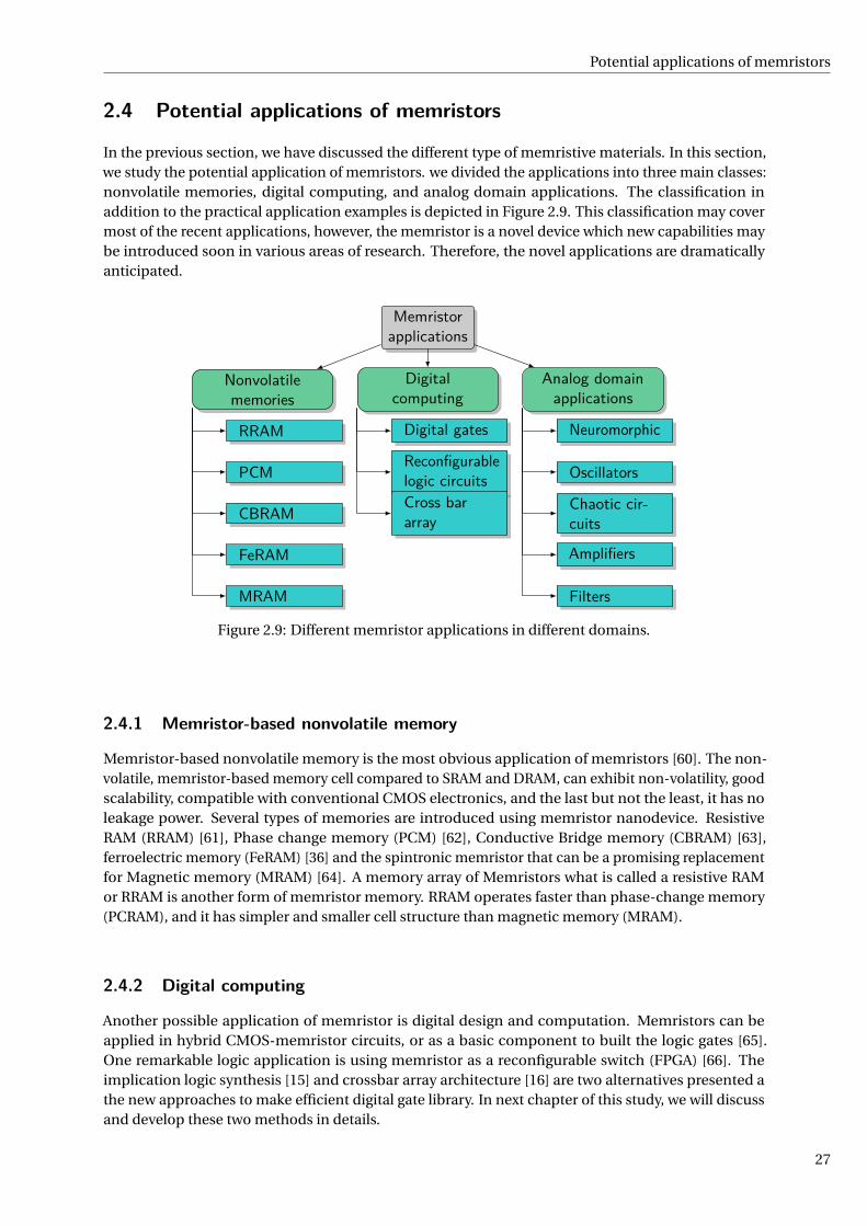
Potential applications of memristors
2.4 Potential applications of memristors
In the previous section, we have discussed the different type of memristive materials. In this section,we study the potential application of memristors. we divided the applications into three main classes:nonvolatile memories, digital computing, and analog domain applications. The classification inaddition to the practical application examples is depicted in Figure 2.9. This classification may covermost of the recent applications, however, the memristor is a novel device which new capabilities maybe introduced soon in various areas of research. Therefore, the novel applications are dramaticallyanticipated.
Memristorapplications
Nonvolatilememories
Digitalcomputing
Analog domainapplications
RRAM
PCM
CBRAM
FeRAM
MRAM
Digital gates
Reconfigurablelogic circuitsCross bararray
Neuromorphic
Oscillators
Chaotic cir-cuits
Amplifiers
Filters
Figure 2.9: Different memristor applications in different domains.
2.4.1 Memristor-based nonvolatile memory
Memristor-based nonvolatile memory is the most obvious application of memristors [60]. The non-volatile, memristor-based memory cell compared to SRAM and DRAM, can exhibit non-volatility, goodscalability, compatible with conventional CMOS electronics, and the last but not the least, it has noleakage power. Several types of memories are introduced using memristor nanodevice. ResistiveRAM (RRAM) [61], Phase change memory (PCM) [62], Conductive Bridge memory (CBRAM) [63],ferroelectric memory (FeRAM) [36] and the spintronic memristor that can be a promising replacementfor Magnetic memory (MRAM) [64]. A memory array of Memristors what is called a resistive RAMor RRAM is another form of memristor memory. RRAM operates faster than phase-change memory(PCRAM), and it has simpler and smaller cell structure than magnetic memory (MRAM).
2.4.2 Digital computing
Another possible application of memristor is digital design and computation. Memristors can beapplied in hybrid CMOS-memristor circuits, or as a basic component to built the logic gates [65].One remarkable logic application is using memristor as a reconfigurable switch (FPGA) [66]. Theimplication logic synthesis [15] and crossbar array architecture [16] are two alternatives presented athe new approaches to make efficient digital gate library. In next chapter of this study, we will discussand develop these two methods in details.
27

CH2. MEMRISTOR NANODEVICE FOR UNCONVENTIONAL COMPUTING: REVIEW AND APPLICATIONS
2.4.3 Analog domain applications
Another further research area of memristive devices is analog domain application. Simple circuits ofmemristors with a single capacitor or inductor are discussed in [67]. There are several research work inanalog domain using memristors such as neuromorphic computing, amplifiers, memristor oscillators,filters and chaotic circuits (see e.g. [68], [69], [70], [71]).
Most interesting and recent study field in analog domain that we will focus on it more in ourresearch is neuromorphic or neuro-inspired computation. It is believed this approach is promising foryielding innovations in future cognitive computing, hence will get probably more attention in the nearfuture of research. The key to the high efficiency of biological neural systems is the large connectivitybetween neurons that offers highly parallel processing power. Another key factor of high efficiency ofbiological neural network is the connection plasticity. The synaptic weight between two neurons canbe precisely adjusted by the ionic flow through them and it is widely believed that the adaptation ofsynaptic weights enables the biological neural systems to learn. Memristors function similarly to thebiological synapses. This characteristic makes Memristors proper building blocks in neuromorphicsystems, where neurons and synapses are modeled as electronic devices [41]. Memristors can be madeextremely small, therefore, by applying them, mimicking the functions of a brain would be possible innear future [44]. The brain-like computing capability of the memristor-based complex spike timing-dependent plasticity (STDP) learning networks is demonstrated by Afifi et al [72].
2.5 Streams of researchThe ability to indefinitely store resistance values means that a memristor can be used as a nonvolatilememory. There are yet more potential applications that we did not mention previously , we point tothe capacity of memristive networks in realizing demanding image processing and more specificallyedge detection and face/object recognition [73]. Pershin and Di Ventra address the capability ofmemristors to perform quantum computation in addition to conventional neuromorphic and digitaldata processing [74]. Performing arithmetic operations in memristor-based structures is possible inboth analog and digital approaches [75]. Another system level application is memristive Neuro-FuzzySystem [76].
However, the memristor potential goes far beyond instant-on computers to embrace one of thebiggest technology challenges: mimicking the functionality of the brain. Within a decade, memristorscould let us emulate, instead of merely simulate, networks of neurons and synapses. By replacingseveral specific transistors with a crossbar of memristors, circuit could be shrunk by nearly a factor of 10
Figure 2.10: Classification of domain studies using memristive devices
28
Conclusions and summary
in area and improved in terms of its speed relative to power consumption performance [44]. Computingwith memristor is another interesting approach which memristor plays a crossbar switch role inthe circuit. Using memristor-based circuit for performing arithmetic operations, signal processingapplication, dynamic load, oscillators, amplifiers, sensing application, artificial biological system,image encryption, and many other approaches are several applications of memristor that recentlyappeared in different research publications. In this context, we made a simple classification of a streamof research as shown in Figure 2.10 that could be useful for those who want to use this flexible devicein their research studies. The hybrid approaches are not in the chart, here we mention that any sort ofutilization can be implemented in hybrid circuit instead of using pure memristive circuit.
2.6 Conclusions and summaryIn this chapter, we have done a feasibility study on memristive nanodevice from theoretical model topractical applications. we studied the cons and pros of using different memristor devices based onthe applied material to manufacture the device. As each material or type of memristor has its owncharacteristics, consequently one can analyze and discover the different potential of application of eachtype of these memristive devices more conveniently. The better understanding of physics of differentmemristive materials leads to discover more sophisticated applications of these devices. Four generalmemristive devices are surveyed namely: Resistive, Spintronic, Organic (polymeric) and Ferroelectricmemristive devices. The potential application as well as advantages versus disadvantages of usingeach one are presented too. The resistive memristor has been applied more than others in differentresearch works from memory to artificial synapse. The Spintronic and Ferroelectric devices showpromising properties to make new nonvolatile memories. The organic memristor is more appropriateto make artificial synapse in Spiking Neural Networks. The mix combination of those materials notonly propose new research studies but also take the advantages of using more useful properties ofeach device.
The practical applications of memristive devices are presented subsequently. Three main domainsof potential applications have been classified: a)nonvoaltile memory such as RRAM, PCM, CBRAM,FeRAM and MRAM; b)digital computing domain such as logic implication and crossbar array; c)analogdomain of application such as neuro-inspired computing in spiking neural networks, oscillators, filtersand amplifiers. Among these applications, we focus on computation approaches by using two digitaland neuromorphic domains.
29


Chapter 3
Unconventional digital computingapproach: memristive nanodevice
platform
Abstract
Memristor is a two-terminal nanodevice that has recently attracted the attention of manyresearchers. Its simple structure, non-volatility behavior, high-density integration, and low-powerconsumption make the memristor a promising candidate to act as a switch in digital gates for futurehigh-performance and low-power nanocomputing applications. In this chapter, we model thebehavior of memristor by using Verilog-A tools. To investigate its characteristics in a circuit, we usethe HSPICE simulator. Furthermore, a library of digital gates is provided by using two approachesto make digital gates: the first one is based on material implication (IMP) and the second one isbased on crossbar arrays. Finally, we compare and evaluate both computation methods.
3.1 IntroductionIt is important to be able to control the states of the conductance of memristor in order to usememristors for computing in general, analog or digital. As the memristor is applied in the differentplatform as a two terminal device for state modification new approaches are required. In traditionalCMOS computing, using transistor state we can switch between ‘0’ and ‘1’ to be able to produceBoolean functions such as NOT, AND, OR and etc. In CMOS-based computing, the switching of thetransistor is controlled by a third terminal, (Base in BJT and Gate in MOSFET). The story of the statecontrolling for memristor nanodevice is different as there are only input and output terminals (noterminal for controlling the states of the switch). Therefore, the new methods and approaches arestudied to be able to use two-terminal devices for computing.
In this chapter, we study and discuss two methods for digital computing by memristive tow-terminal devices mainly based on our publication [13]. There are two main approaches, namelymaterial implication (IMP) or stateful logic and programmable crossbar architecture that are discussedin this chapter. Material implication was studied by Whitehead and Russell in early 1900s in PrincipiaMathematica [77]. IMP can be implemented on memristor with couple of sequences of controlvoltages. In this study based on previous research works on IMP, we establish a functionally completeBoolean operation to be able to build other standard logic gates. The second method, combination ofmemristor with crossbar interconnect technology, has been demonstrated as offering the potential ofcreating configurable electronic devices with applications in digital computation, signal processingand artificial intelligence [17]. In this chapter, we analyze the application of crossbar array architecturein constructing logic building blocks. Our contribution is to present a comprehensive library to build
31

CH3. UNCONVENTIONAL DIGITAL COMPUTING APPROACH: MEMRISTIVE NANODEVICE PLATFORM
RG
VsetVcondA B
A B
0
01
1
0
1
0
1
B'
1
10
1
in in outa b
Figure 3.1: Memristor-based IMP: a) circuit schematic, b) IMP truth table.
a complete set of Boolean gates using both approaches. At the end of this chapter we evaluate andcompare both methods.
The logic computing applications of memristor have been investigated by several researchers[12, 14–17, 78–81]. For instance, Borghetti et al. [12] used material implication (IMP) logic operationto carry out logic computation by using memristors. In IMP approach, A IMP B (A→B) operationmeans ‘if A, then B ’ and can be read as A implies B . IMP together with a FALSE gate are able to form afunctionally complete set (any Boolean function can be expressed). By applying memristor as a digitalswitch, a high memristance (memristor resistance) is considered as logic ‘0’ and a low memristance isconsidered as logic ‘1’. Another approach to make gates by a two-terminal device as a switch is theprogrammable crossbar architecture [16, 17]. The crossbar nanowire array architecture can be used tocompute logic functions by using memristor as a switch between two nanowires [78].
3.2 Stateful implication logic
One of the basic potential applications of memristors is to utilize them in building blocks of logicgates. Therefore, by applying a digital pulse voltage to the memristor terminals, we have a switchwith ON or OFF state. Unlike conventional CMOS, in memristor-based gates, data will be stored asa resistance rather than a voltage. In this case, the latches are non-volatile. Thus, RON displays logic‘1’ which means closed switch and ROF F displays ‘0’ for presenting open switch. In contrast to thethree-terminal CMOS-based transistor as a switch, in a two-terminal switch, there is no terminal tocontrol ON or OFF states of the switch. Consequently, instead of conventional Boolean logic, we shouldfind other substitutes to create a logic gate.
IMP (Figure 3.1.a) is a way to use one memristor to control the other one. IMP is recognized asa promising method for making gates by memristors [12, 15, 80, 82]. In IMP structure, memristorshave different roles in different stages of the computing process: input, output, computational logicelement, and a latch depending upon which write, read, computing and storing processes are takingplace, respectively.
To figure out how IMP operates, imagine A as a question and B as an answer to that question. If thequestion is wrong, any answer (wrong or correct) makes a true output (logic 1), as depicted in Figure3.1.b. The only case for the false (logic 0) output would be a wrong answer to a correct question. So theimplication logic is equivalent to function (¬A)∨B . Figure 3.1.a shows the basic circuit of memristorsA and B to perform implication logic, which are formed by the vertical nanowire crossing over thehorizontal nanowire connected to a load resistor RG . After the operation of material implications, theresult is stored as the state of switch B (B ′) while A is left unchanged.
To switch between logic ‘1’ to logic ‘0’ (and vice versa), we need a tri-state voltage driver with ahigh impedance output state when it is undriven. Vset is a negative voltage which should be applied toits corresponding tri-state driver. Vset can switch memristor to conductive state with low resistanceRON . Similarly, the positive voltage Vclear is required to change the memristive switch state to low-conductance (high-resistance) state ROF F . It is important to mention that the magnitude of Vset
32

Stateful implication logic
and Vclear must be larger than device threshold voltage for switching ‘ON’ and ‘OFF’. In order toremain in a specific state (line 3 in truth table 3.1.b), the Vcond is applied as a negative voltage with amagnitude smaller than Vset . Consequently, tri-state drive —since is not in high-impedance state— ispulsed by one of the Vset , Vclear or Vcond . By applying Vcond and Vset to A and B simultaneously, thememristive IMP operates properly. Although the conditional voltage (Vcond ) is not necessary, exceptfor the case AB=‘10’ (third line in the truth table Figure 3.1.b), it is possible to either apply Vcond oruse high-impedance (HZ) for all other cases. If Vset is applied to B alone, it would be unconditionallylogic ‘1’, nevertheless applying Vcond by itself to A does not change its state. On the other hand, if bothvoltages are applied together, the present state of switch A determines the next state of switch B . IfA=‘0’, it means memristor A is in high resistance state (ROF F ). Therefore, there is a small voltage dropacross RG . In this case, B will be set and A is left unchanged. Alternatively, if present state of A=‘1’,switch A is in low resistance state and Vcond drops across RG , so both A and B remain unchanged. Itshould be noted that the RG value must be chosen such that RON<RG<ROF F , where RON and ROF F
are resistance states of ‘ON’ and ‘OFF’ switches, respectively.
RG
VBVAA B
A
0
01
1
0
0
1
1
0
a
c
VC
C
C
0
00
0
C
0
0
C'Step 1 Step 2 Step 3
B
0
0
1
1
1
0
1
11
0
C'
0
1
C" A
0
01
1
0
0
1
11
01
1
C"B
0
NAND Truth Table
b
StepsVoltage Pulses
VA VB VC
123
Vclear
Vset
Vset
Vcond
Vcond
Operation
C=0
A IMP C
B IMP C
HZ=High Impedance
HZ HZ
HZ
HZ
Figure 3.2: NAND configuration with IMP: a) circuit schematic, b) required voltages for controlling the process,c) sequential truth table to obtain NAND.
3.2.1 Functionally complete Boolean operationsIn Boolean logic algebra, a set of logic operations is called functionally complete if all other logicfunctions can be constructed from combining the members of this set. The single-element setsNAND (AND, NOT) and NOR (OR, NOT) are functionally complete operations. In addition, it hasbeen demonstrated that all Boolean expressions can then be written in one of the standard normalforms using only a (IMP) operation and a false (Inverse) operation [12, 80]. In fact, to show that thememristive implication logic is a functionally complete operation; the easiest way is to synthesize theNAND function with it.
A circuit with three memristors A, B , and C is illustrated schematically in Figure 3.2.a. Assume twoimplication operations being performed subsequently, first A IMP C and then B IMP C . Hence A andB are inputs and C is output. The final output result is represented with variable C′′ in Figure 3.2.c.Firstly, Vclear should be applied to switch C to create the false operation (C ′ = (C IMP 0)). By applyingVcond and Vset pulses to A and C respectively, the second step would be performed. Finally, C ′′ = (BIMP C ) is yielded by applying Vcond to VB and Vset to VC (see Figure 3.2.b and Figure 3.2.c). In otherwords, the resulting state of switch C can be written as:
C = B IMP (A IMP C ) =¬B ∨ ((¬A)∨C )
if C = 0 initially then
C =¬B ∨ ((¬A)∨0) = (¬B)∨ (¬A)
=¬(A∧B)
33
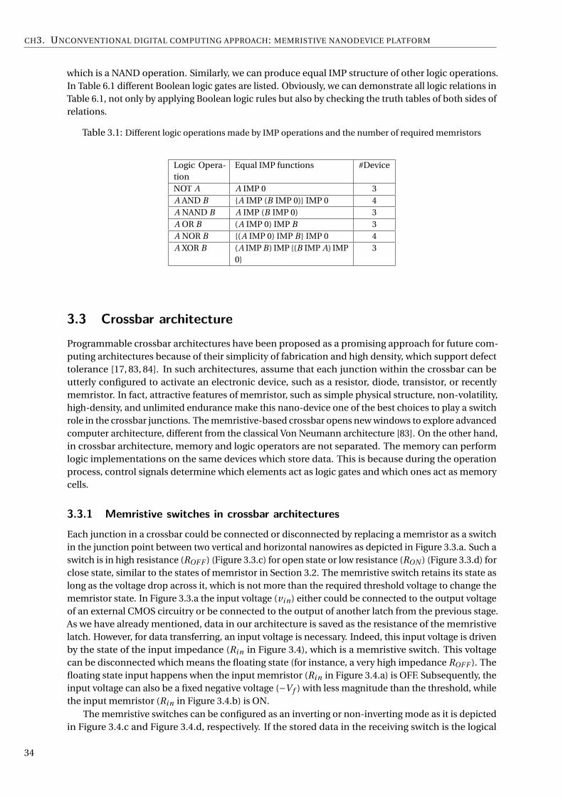
CH3. UNCONVENTIONAL DIGITAL COMPUTING APPROACH: MEMRISTIVE NANODEVICE PLATFORM
which is a NAND operation. Similarly, we can produce equal IMP structure of other logic operations.In Table 6.1 different Boolean logic gates are listed. Obviously, we can demonstrate all logic relations inTable 6.1, not only by applying Boolean logic rules but also by checking the truth tables of both sides ofrelations.
Table 3.1: Different logic operations made by IMP operations and the number of required memristors
Logic Opera-tion
Equal IMP functions #Device
NOT A A IMP 0 3A AND B A IMP (B IMP 0) IMP 0 4A NAND B A IMP (B IMP 0) 3A OR B (A IMP 0) IMP B 3A NOR B (A IMP 0) IMP B IMP 0 4A XOR B (A IMP B) IMP (B IMP A) IMP
03
3.3 Crossbar architectureProgrammable crossbar architectures have been proposed as a promising approach for future com-puting architectures because of their simplicity of fabrication and high density, which support defecttolerance [17, 83, 84]. In such architectures, assume that each junction within the crossbar can beutterly configured to activate an electronic device, such as a resistor, diode, transistor, or recentlymemristor. In fact, attractive features of memristor, such as simple physical structure, non-volatility,high-density, and unlimited endurance make this nano-device one of the best choices to play a switchrole in the crossbar junctions. The memristive-based crossbar opens new windows to explore advancedcomputer architecture, different from the classical Von Neumann architecture [83]. On the other hand,in crossbar architecture, memory and logic operators are not separated. The memory can performlogic implementations on the same devices which store data. This is because during the operationprocess, control signals determine which elements act as logic gates and which ones act as memorycells.
3.3.1 Memristive switches in crossbar architectures
Each junction in a crossbar could be connected or disconnected by replacing a memristor as a switchin the junction point between two vertical and horizontal nanowires as depicted in Figure 3.3.a. Such aswitch is in high resistance (ROF F ) (Figure 3.3.c) for open state or low resistance (RON ) (Figure 3.3.d) forclose state, similar to the states of memristor in Section 3.2. The memristive switch retains its state aslong as the voltage drop across it, which is not more than the required threshold voltage to change thememristor state. In Figure 3.3.a the input voltage (vi n) either could be connected to the output voltageof an external CMOS circuitry or be connected to the output of another latch from the previous stage.As we have already mentioned, data in our architecture is saved as the resistance of the memristivelatch. However, for data transferring, an input voltage is necessary. Indeed, this input voltage is drivenby the state of the input impedance (Ri n in Figure 3.4), which is a memristive switch. This voltagecan be disconnected which means the floating state (for instance, a very high impedance ROF F ). Thefloating state input happens when the input memristor (Ri n in Figure 3.4.a) is OFF. Subsequently, theinput voltage can also be a fixed negative voltage (−V f ) with less magnitude than the threshold, whilethe input memristor (Ri n in Figure 3.4.b) is ON.
The memristive switches can be configured as an inverting or non-inverting mode as it is depictedin Figure 3.4.c and Figure 3.4.d, respectively. If the stored data in the receiving switch is the logical
34

Crossbar architecture
Vcontrol
Vin Vout
Unknown State
Open State Close State
Memristor as a switch a b
c d
Figure 3.3: Different states of a switch in a crossbar array.
complement of the input data, the configuration is in the inverting mode. If the stored data is thesame as the input data the configuration is in the non-inverting mode. Different control signals makedifferent configurations. Inverting configuration requires three steps to perform the appropriate latchoperation:1) We preset the switch unconditionally open (Figure 3.4.a) by applying a positive voltage (more thanthe positive threshold) to the control of the vertical nanowire and also by forcing input to the highimpedance mode. A diode is also required to provide a low-impedance path to the ground to protectthe junction.2) If the input voltage is logic ‘1’ then Ri n=RON and −V f drops across RG , so the voltage acrossmemristor is not enough to close it and the switch remains OFF. On the other hand, when input is logic‘0’, then Ri n=ROF F and the memristor switch turns ON. Thus, the junction has held the inverted stateof the input (see Figure 3.4.b).3) The input signal must be in the high impedance (disconnected). The state of the switch is readout onto the horizontal nanowire. This is accomplished by driving the vertical nanowire with a smallvoltage whose magnitude is less than the threshold control voltage (can not change the switch state).We call this voltage vR (Read voltage).For non-inverting configuration, as depicted in Figure 3.4.d, the pull-down resistor RG is not requiredwhen writing the state of the driving switch to the receiving one. The steps for appropriate latchoperation are the same as the ‘inverting configuration’ except grounding the vertical nanowire of thedriving switch rather applying a negative voltage in conditionally close step. In this case, by applyingthe negative voltage to the vertical control line, the receiving switch will be close if the driving switch isclose (low-impedance path to the ground) and the receiving switch remains open if the driving switchis open. Thus, the state of the first switch is replicated in the second switch.
3.3.2 Configurable crossbar array logic gates
In this section, we demonstrate how to make a gate by using the crossbar approach. We start usingcrossbar to make a 3-input AND gates. Figure 3.5.a shows a crossbar array which consisting of 8memristors. We need three inputs A, B, and C, each of which is assumed to be impedance encoded.Basically, various voltages are applied to vertical nanowires to control the memristive switches. Theinputs are connected to the horizontal wires as represented in Figure 3.5.a. The crossbar array functionsas an AND gate by applying the following sequences.
1. All junctions are unconditionally opened by applying a positive voltage higher than the thresholdvoltage to the vi n , vand , vout control vertical lines.
35
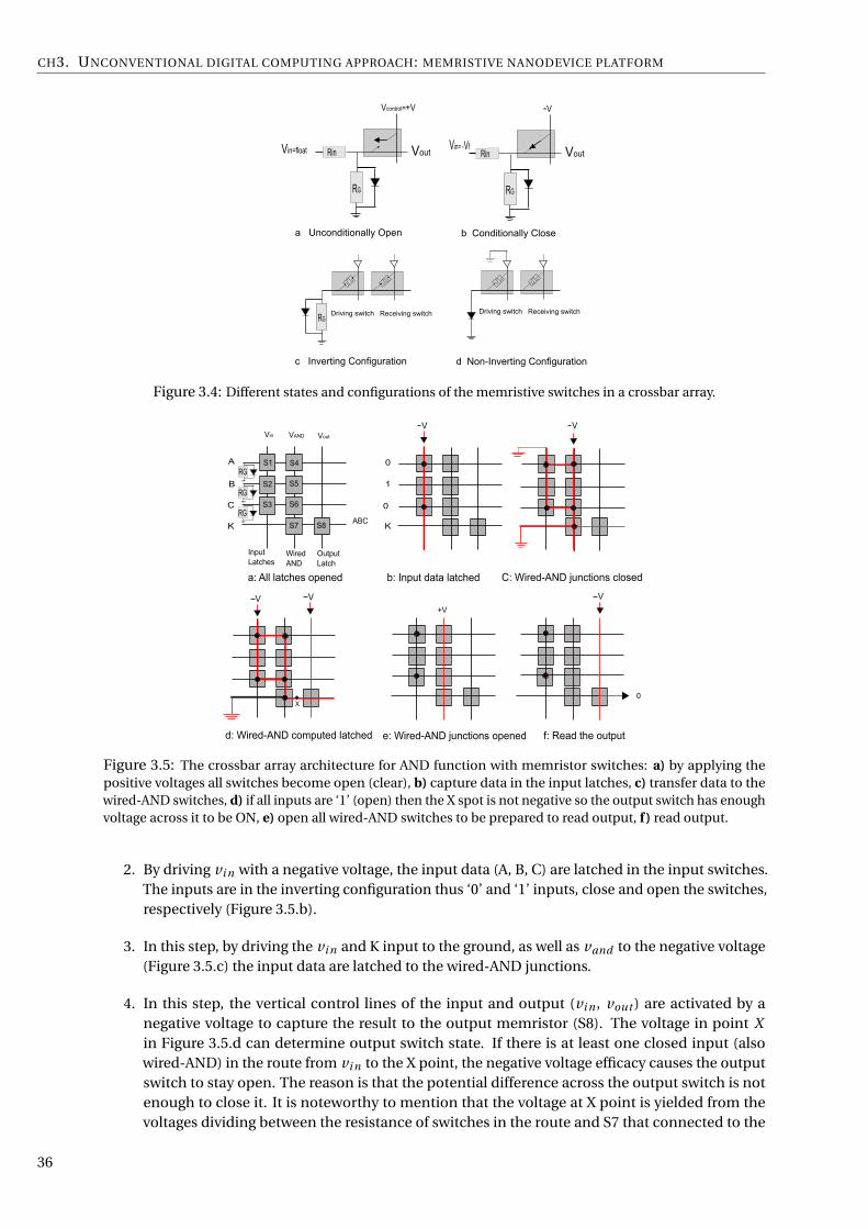
CH3. UNCONVENTIONAL DIGITAL COMPUTING APPROACH: MEMRISTIVE NANODEVICE PLATFORM
Vcontrol=+V
Vin=float Vout
a Unconditionally Open b Conditionally Close
c Inverting Configuration d Non-Inverting Configuration
RG
Rin
RG
Rin
RG
-V
Vin= -Vf Vout
Driving switch Receiving switch Driving switch Receiving switch
Figure 3.4: Different states and configurations of the memristive switches in a crossbar array.
A
B
C
K
Vin VAND Vout
Input Latches
WiredAND
OutputLatch
a: All latches opened
0
1
0
KABC
b: Input data latched C: Wired-AND junctions closed
V V
0
VV+V
d: Wired-AND computed latched e: Wired-AND junctions opened f: Read the output
S1 S4
S2
S3
S5
S6
S7 S8
V
RG
X
RG
RG
Figure 3.5: The crossbar array architecture for AND function with memristor switches: a) by applying thepositive voltages all switches become open (clear), b) capture data in the input latches, c) transfer data to thewired-AND switches, d) if all inputs are ‘1’ (open) then the X spot is not negative so the output switch has enoughvoltage across it to be ON, e) open all wired-AND switches to be prepared to read output, f ) read output.
2. By driving vi n with a negative voltage, the input data (A, B, C) are latched in the input switches.The inputs are in the inverting configuration thus ‘0’ and ‘1’ inputs, close and open the switches,respectively (Figure 3.5.b).
3. In this step, by driving the vi n and K input to the ground, as well as vand to the negative voltage(Figure 3.5.c) the input data are latched to the wired-AND junctions.
4. In this step, the vertical control lines of the input and output (vi n , vout ) are activated by anegative voltage to capture the result to the output memristor (S8). The voltage in point Xin Figure 3.5.d can determine output switch state. If there is at least one closed input (alsowired-AND) in the route from vi n to the X point, the negative voltage efficacy causes the outputswitch to stay open. The reason is that the potential difference across the output switch is notenough to close it. It is noteworthy to mention that the voltage at X point is yielded from thevoltages dividing between the resistance of switches in the route and S7 that connected to the
36

Crossbar architecture
ground in the last horizontal nanowire line.
5. By driving a positive voltage to vand , all junctions in this column will be opened (Figure 3.5.e).
6. The AND of the three inputs is stored in the output switch and is ready to be read out.
If the output switch is at inverse mode (inverting configuration), the crossbar array becomes a 3-input NAND gate. Moreover, the crossbar array can also become a 3-input NOR gate, if RG ’s areremoved while input data are applied to the circuit (Non-inverting configuration). By inverting thelast output with the recent situation of the inputs, the crossbar architecture becomes a 3-input ORgate. Consequently, all logic gates are created except XOR and XNOR, which require a little differentstructures. First, we create an exclusive-NOR gate, subsequently, by inverting the output, XOR isobtained. To implement XNOR, two midterms should be OR’ed together. The crossbar array operationfor creating XNOR is similar to AND crossbar array in Figure 3.5. However, three additional steps arerequired. To simplify the crossbar array, we apply two variables A and B (Figure 3.6). In the following,we discuss these sequences step by step.
1. All junctions are unconditionally opened by applying a positive voltage to the vi n , two v AN D ’s,and vout control lines.
2. By driving vi n with a negative voltage, the input data (A, B , A, B) are latched in the input switches.The inputs are in the inverting configuration, therefore, ‘0’ and ‘1’ inputs close and open theswitches, respectively.
3. In this step, by driving the vi n and K input to the ground, and v AN D1 to the negative voltage, theinput data are latched to the wired-AND for the first minterm.
4. In this step, the vertical control lines of input and output (vi n , vout ) are activated by a negativevoltage for first minterm to capture the result (AB) to the output.
5. By applying the positive voltage to v AN D1 (the wired-AND), junctions become open for the firstminterm.
6. For the second minterm implementation, step 3 should be repeated by applying a negativevoltage to v AN D2.
7. In this step, the control lines of input and output (vi n , vout ) are activated by a negative voltage forthe second minterm to capture the result (AB) to the output. It is worth to note that performingOR of the two minterms is sequential rather than concurrent. It means that if the output switchis set into the close state by the first minterm, the value of the second minterm has no effect.Otherwise, changing the state of the output switch is dependent on the second minterm.
8. By applying the positive voltage to the v AN D2, the wired-AND junctions become open for thesecond minterm.
9. The XNOR of two inputs A and B is stored in the output switch and it is ready to be read out.
It is also possible to make other Boolean logic functions by applying NAND combinations. However,it requires a larger number of memristive switches. Furthermore, it nullifies the most importantcapability of memristors, i.e. configurability.
37

CH3. UNCONVENTIONAL DIGITAL COMPUTING APPROACH: MEMRISTIVE NANODEVICE PLATFORM
A
B
K
Vin VAND1 Vout
Input Latches Wired ANDs
OutputLatch
RG
RG
RG
A
BRG
VAND2
A B AB
A B Figure 3.6: Crossbar array architecture for exclusive-NOR function.
3.4 EvaluationIn this section, we present an evaluation of both the IMP and crossbar array approaches. Bothapproaches have significant advantages over the CMOS-based logic gates, such as having computationand storing using the same physical unit, non-volatility, and small scalability because of the natureof memristive switches. By applying the IMP method, the number of memristors to make a gate canbe saved. The less number of memristive switches causes less power consumption and cost. Table3.2 provides the number of memristors required to make various logic gates in both cases. We note
Table 3.2: The number of memristive switches to make logic gates for the imp and crossbar array approaches.
Logic Operation #IMP #Crossbar ArrayS ← NOT A 2 3S ← A AND B 4 6S ← A NAND B 3 6S ← A OR B 6 6S ← A NOR B 6 6S ← A XOR B 7 11
that the number of memristors to make gates in the IMP approach in Table 3.1 is different from Table3.2. When logic operations listed in Table 3.1 operate on two variables A and B , the original logicwould be lost during the implication process. For instance, in case of NAND, only B is changed and incase of XOR both A and B will change. Therefore, to store data we require the additional number ofmemristive switches. For a more detailed explanation see [75]. Despite the overhead introduced in thecrossbar approach in terms of number of memristors, it can dynamically adapt its logic function bycontrolling voltages. Therefore, based on the run-time requirements, the crossbar array approach isadaptable and reconfigurable.
3.5 ConclusionsIn this chapter, based on the electrical model of the memristor is represented in Chapter 2, we showhow physical properties of this device can be utilized for digital circuit applications. Memristor isa two-terminal device, therefore, we need new approaches to apply it to operate as a switch. IMP
38

Conclusions
logic with memristor is studied as the first method to create digital gates. We demonstrated thatby using IMP and the inverse function (NOT), it is possible to produce all digital Boolean functions.In the IMP approach, the number of memristors to make gates are fewer than the crossbar arrayapproach. We proposed the crossbar array architecture as the second novel promising techniquefor nanocomputing binary paradigm. The crossbar array method with memristive switches hasbeen investigated comprehensively. Reconfigurability is the most significant advantage of using thecrossbar array architecture. It is interesting to note that in both computing techniques, the storing andcomputing units are physically the same. This property has the potential to overcome the memorybottleneck. For future work, one can organize a Programmable Logic Device (PLA) platform in such away that the crossbar array operates as a programmable AND array beside IMP as a fixed connectionfor the OR array.
39

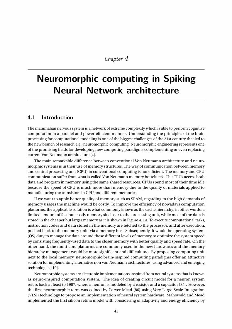
Chapter 4
Neuromorphic computing in SpikingNeural Network architecture
4.1 Introduction
The mammalian nervous system is a network of extreme complexity which is able to perform cognitivecomputation in a parallel and power-efficient manner. Understanding the principles of the brainprocessing for computational modeling is one of the biggest challenges of the 21st century that led tothe new branch of research e.g., neuromorphic computing. Neuromorphic engineering represents oneof the promising fields for developing new computing paradigms complementing or even replacingcurrent Von Neumann architecture [4].
The main remarkable difference between conventional Von Neumann architecture and neuro-morphic systems is in their use of memory structures. The way of communication between memoryand central processing unit (CPU) in conventional computing is not efficient. The memory and CPUcommunication suffer from what is called Von Neumann memory bottelneck. The CPUs access bothdata and program in memory using the same shared resources. CPUs spend most of their time idlebecause the speed of CPU is much more than memory due to the quality of materials applied tomanufacturing the transistors in CPU and different memories.
If we want to apply better quality of memory such as SRAM, regarding to the high demands ofmemory usages the machine would be costly. To improve the efficiency of nowadays computationplatforms, the applicable solution is what commonly known as the cache hierarchy; in other words, alimited amount of fast but costly memory sit closer to the processing unit, while most of the data isstored in the cheaper but larger memory as it is shown in Figure 4.1.a. To execute computational tasks,instruction codes and data stored in the memory are fetched to the processor, and after execution,pushed back to the memory unit, via a memory bus. Subsequently, it would be operating system(OS) duty to manage the data around these different levels of memory to optimize the system speedby consisting frequently-used data to the closer memory with better quality and speed rate. On theother hand, the multi-core platforms are commonly used in the new hardwares and the memoryhierarchy management would be more significant and difficult too. By proposing computing unitnext to the local memory, neuromorphic brain-inspired computing paradigms offer an attractivesolution for implementing alternative non von Neumann architectures, using advanced and emergingtechnologies [19].
Neuromorphic systems are electronic implementations inspired from neural systems that is knownas neuro-inspired computation system. The idea of creating circuit model for a neuron systemrefers back at least to 1907, where a neuron is modeled by a resistor and a capacitor [85]. However,the first neuromorphic term was coined by Carver Mead [86] using Very Large Scale Integration(VLSI) technology to propose an implementation of neural system hardware. Mahowald and Meadimplemented the first silicon retina model with considering of adaptivity and energy efficiency by
41

CH4. NEUROMORPHIC COMPUTING IN SPIKING NEURAL NETWORK ARCHITECTURE
core 1
Local Memory
core 2
Local Memory
Shared Memory Cache
CPU
Main Memory
Prepheral Memory
a:
b:
Synapse(Local Memory)
Neural Network
Neuron (core)
Figure 4.1: Computational architecture a) Von Neumman architecture, fast and costly memory are closerto cores in multiprocessor platforms as cashes and local memory as well as inexpensive and slower memoryare in other layers close to magnetic memory to save the cost of CPU (memory hierarchy). b) Neuromorphicarchitecture inspired from neural networks in the biological brain, capable to conquer Von neumann bottelneckissue, performing parallel and cognitive computing, as well as considering that the synapses are local memoriesconnected to each neurons as computational cores.
simulating retina functionalities [87]. Tobi Delbruck built on the idea of adaptive photoreceptor circuitsdeveloped in [88] and presented approaches for enhancing retinomorphic sensors consist of 128×128pixel Dynamic Vision Sensor (DVS). DVS established a benchmark in neuromorphic vision domainwith introducing Address Event Representation (AER) sensory data in which each individual pixelprocessed the normalized time derivative of the sensed light and provided an output in the form ofspikes of the pixel addresses. In addition to vision sensory neuromorphic research, there are severalneuromorphic studies using auditory and olfactory sensors [89–91] for review study in neuromorphicresearch using different sensory inputs, we refer the readers to [92].
More close to our research, in 2014 two distinguished articles were published that increasedthe scientists attentions to the general neuromorphic platforms as novel computing architectures.Merolla et al. [18] in an IBM research was sponsored by DARPA, have demonstrated a computinghardware consist of the compact modular core for large-scale neuromorphic system architecture. Thecores combine digital neurons with the large synaptic array. This general purpose neuromorphicprocessor was built using thousands of neurosynaptic cores are involved one million neurons and 256million of reconfigurable synapses. The second notable work published in 2014 was Spiking NeuralNetwork Architecture (SpiNNaker) project [29]. The SpiNNaker project is a decade old, comprehensivedescription of the project is announced in [29]. SpiNNaker project aims to deliver a massively parallelmillion core architectures whose interconnections are inspired by the connectivity properties of themammalian brain. The hardware platform is suitable to model the large-scale spiking neural networksin biological real time. Neuromorphic and neuro-inspired computing is now being adapted by anincreasing number of academic and industrial different research teams. In recent few years, there havebeen many valuable publications explaining the use of novel materials are able to emulate some of theproperties observed in biological synapses [19, 30, 41, 93–95].
Our work focuses on an alternative approach aimed at high performance computation to realizethe compact, parallel, cognitive and energy-efficient architecture structure that emulate the style of
42

Spiking Neural Networks
computation of the biological brain, using the Spiking Neural Network (SNN) structure, modelingthe neurons as computational cores next to memristive artificial synapses as local memories to skipmemory delay bottelneck similar to what is shown in Figure 4.1.b. Therefore, it is necessary to define,analyze and verify the efficient models of network topology, neuron and synapse models based onstate-of-the-art technologies besides choosing the optimized learning model adapted to our platformand devices. The structure of Chapter 4 is followed by reviewing SNN and more significantly the func-tionality of various spike information codings. In the same section, we discuss different neural networktopologies. Furthermore in the Section 4.3, different models of neuron is presented. Synapse andlearning are explained in the Section 4.4 which various methods of spike-timing-dependent plasticity(STDP) [22,23] are studied comprehensively. The state-of-the-art of the most important neuromorphicplatforms and projects in the world is presented in 4.5. Lateral inhibition and Homeostasis have beendiscussed at the discussion part of this chapter.
4.2 Spiking Neural Networks
Artificial neural networks (ANN) can generally be categorized into three generations. The first genera-tion of neural network consisted of McCulloch and Pitts neurons [96] that the output signals are limitedto discrete ’0’ or ’1’ binary values. Perceptrons, Hopfield network, Boltzmann machine and multilayernetworks with threshold units are ANN examples that are classified in first generation. The secondgeneration of neural network, by using a continuous activation function such as sigmoid, polynomialor exponential functions, the output can take analog values between ’0’ and ’1’. Due to using analogoutput the network requires less neurons than the first generation class. Radial Basis Function (RBF)networks and Multi-Layer Perceptrons (MLP) are categorized under second generation class. The thirdgeneration of neural network model are networks which employ spiking neurons as computationalunits. In this model, the precise firing times of neurons are used for information coding. Spiking neuralnetworks belong to the third generation of neural networks.
Indeed, artificial neural network in the first and second generation is a mathematical model ofmammalian brain though, SNN is an electronic hardware neuromorphic model of the biologicalbrain. Networks composed of spiking neurons are able to process significant amount of data usinga relatively small number of spikes [97]. Due to the similarity between the biological neurons andspiking models functionality, SNNs provide powerful tools to emulate data processing in the brain,including neural information processing, plasticity and learning. Consequently, spiking networksoffer solutions to a broad range of specific problems in applied engineering image detection, eventdetection, classification, speech recognition and many cognitive computation domain applications.
4.2.1 Spike information coding
Spike is the language of neuron communication in SNN architectures. One of the key unresolvedquestions in neuroscience is how information processed in the brain. The nature of the neural code isan unresolved topic of research in neuroscience. However, based on what is known from biology, anumber of neural information encoding have been proposed:
1. Rate codingThe rate of spikes in a time-window is counted for the information transmission. It is also calledas frequency coding (Figure 4.2.a). As the intensity of a stimulus increases more, the firing rateof spikes increases more too. Rate encoding is motivated by the observation that biologicalneurons eager to fire more often for stronger stimuli. There are two types of rate coding namelyspike-count rate and time-dependent firing rate. In spike-count rating by counting the numberof spikes that are generated during a trial and dividing by the duration of the trial, we calculatethe temporal average of rating. In independent firing rate, the average number of spikes overtrial happens during a short interval between times t and t+∆t , divided by the duration of the
43

CH4. NEUROMORPHIC COMPUTING IN SPIKING NEURAL NETWORK ARCHITECTURE
interval. Brette [98] has compared these two approaches in rate information coding in moredetails.
2. Latency codingIn this model, information is supposed to be contained in the exact timing of a set of spikesrelative to each other as it is shown in Figure 4.2.b. It is already proved that precisely timedpatterns of spikes have been postulated to play a significant role in the networks of neuron indifferent functions [99]. Precise spike timing is one of the important parameters that controlvariety forms of synaptic plasticity. Latency coding by using sequences of spikes are mainlyobserved in feed-forward networks since noise and dynamics of recurrent networks can disruptspike timing precision, some attempts to harvest precise spiking timing in recurrent networkshave been done for example by exploring the idea of reservoir computation [100].
3. Phase codingThis model generates the times of emitted spikes based on the time point in a periodic signal.In this (Figure 4.2.c) method the spike trains can encode information in the phase of a pulserespecting to the background oscillations. Phase coding method has been used both in modelsand experimentally. Phase coding has been suggested for the hippocampus as well [101]. Spikingnetworks exploring the phase coding strategy have recently been applied in tasks as olfactorysystems or robot navigation [102].
4. Rank-coding (spike-order coding)In this method of spike coding, information is encoded by the order of spikes in the activity of agroup of neurons as it is depicted in Figure 4.2.d. Rank-coding approach has been suggestedto describe ultra-fast categorization observed in the visual system. This model assumes thateach neuron emits only a single spike during a presentation of the image. This method canbe implemented in a feed-forward network with inhibitory feedback connections. Thorpe andothers [103] developed a spiking neural model that was able to classify static images with aprocessing speed comparable to that observed in humans one.
5. Population codingThis coding model is a method to introduce stimuli by applying the joint activities of the groupof neurons. In population coding, each neuron has a distribution of responses to the certainset of inputs, and the responses of group of neurons will be combined to present a value forthe inputs (Figure 4.2.e). During the last two decades, the theory has focused on analyzing themethods in which different parameters that characterize neuronal responses to external stimuliaffect the information content of these responses. Recent challenge in population coding is todevelop a theory that can generate predictions for specific readout mechanisms for example forvisual target information [104].
6. Sparse codingThis model of coding generally refers to a representation where a few number of neurons areactive, with the majority of the neurons inactive or showing low activity see Figure 4.2.f. Sparsecoding has been suggested as a guiding principle in neural representations of sensory input,specially in the visual sensory system. It is also discussed that sparse coding offers a usefulsolution to the problem of representing natural data because such a scheme allows the system totake advantage of the sparse structure of the sensory environment. It is believed that the naturalenvironment is inherently sparse and codes that using this structure can be both metabolicallyefficient and useful for learning. Sparseness can be defined over a population of neurons at aspecific point in time (population sparseness) or it can be measured for a single neuron over acertain time-window [105].
44

Spiking Neural Networks
a:Stimulus
b:
∆t 1 ∆t3
n1
n2
n3
n4
c:n1
n2
n3
n4
d:n1
n2
n3
n4
1
2
3
4
e:
∆t2
n1
n2
n3
More Excitable
Less Excitable
f:
010
110
010
110
000
111
100
n1
n2
n3
Figure 4.2: Spike information coding strategies a)Rate coding, b)Latency coding, c)Phase coding, d)Rank-coding(spike-order coding), e)Population coding, f ) Sparse coding.
4.2.2 Network topology
The interconnection structure of neurons in a network of neurons is called topology, architecture orgraph of an artificial neural network. The manner in which the interconnection is structured intimatelyis linked to the learning algorithms applied to train the neural networks. Indeed, the interconnectioncan be structured in numerous ways results in numerous possible topologies that are divided intotwo basic classes namely: Feed-Forward Neural Networks (FFNN) and Recurrent (or feedback) NeuralNetworks (RNN) depicted in Figure 4.3.
a: b:
Input layer:
Hidden layer:
Output layer:
Figure 4.3: two main topologies of artificial neural network architectures a)Feed-Forward Neural Networks(FFNN), b) Recurrent Neural Networks (RNN).
45

CH4. NEUROMORPHIC COMPUTING IN SPIKING NEURAL NETWORK ARCHITECTURE
Feed-Forward Neural Networks (FFNN)
The FFNN is divided into two different structure called single-layer FFNN and multilayer FFNN. Thesingle-layer is structured as an input and output layer which is strictly a feed-forward or acyclic graph.We do not count the input layer because no calculation is performed in input nodes (neurons). Themultilayer FFNN has one or more hidden layers between input and output layers similar to Figure4.3.a which has one hidden layer. By adding one or more hidden layers, the neural network can extractthe higher-order statistics which is particularly valuable when the size of the input layer is large [106].Among the known types of neural networks (NN), the feed-forward neural networks are the mostlyused because of their simplicity, flexible structure, good qualities of representation, and their capabilityof universal approximation. Respecting to the way of interconnectivity of the nodes (neurons) thereare two kinds of feed-forward architecture:
fully connectedIn this configuration, every node in each layer of the network is connected to every other node inthe next layer. In fact, we can call them globally connected networks. The Restricted BoltzmannMachine (RBM) could be an example of fully connected FFNN.
partially connectedIn this configuration, some communication links are missing. The convolutional neural networksis a good example for the partially connected FFNN. Partially connected topologies present asuitable alternative with a reduced degree of redundancy and thus a potential for increasedefficiency of neural networks.
Recurrent Neural Networks (RNN)
The RNN is distinguished from FFNN in that it has at least one feedback loop connection. Recurrentneural networks can be single-layer or multilayer as well. Unlike feed-forward neural networks,recurrent networks retain a state that can represent information from an arbitrarily long contextwindow. Although recurrent neural networks have traditionally been difficult to train, and oftencontain thousands of parameters, recent studies in network architectures, optimization techniques,and parallel computation have enabled successful large-scale learning to use RNN [107]. Hopfield [108]network is an example of the recurrent artificial neural network that is used to store one or morestable vectors. The stable vectors can be considered as memories that the network recalls them whenprovided with similar vectors that operate as a queue to the network memory. Other example of RNN isElman network [109] that refers as a simple Recurrent Network is the special case of recurrent artificialneural networks. This type of artificial neural network has the memory that allows it to both detectand generate time-varying patterns.
Modern Neural networks
Here, we discuss recent feed-forward promising neural network which has been applied in differentsensory computation applications.
Convolutional Neural Networks (CNN) Convolutional network is a multi-layer feed-forwardnetwork architecture in which neurons in one layer receive inputs from multiple neurons in theprevious layer and produce an output which is a threshold or sigmoidal function of the weightedsum of its inputs. The connectivity pattern between the nodes of one layer and the node of thesubsequent layer, responsible for the weighted sum operation forms the convolution kernel.Each layer mainly has one or few number of convolution kernels that link the activity of a set ofneurons from one layer to the target neuron of the next layer [20]. Convolutional neural networkswhich have been explored intensively within the neuromorphic community for visual processingtasks [110]. They are normally implemented on CPUs and GPUs which consume a significantamount of power. In recent years, System-On-Chip (SOC) solutions and FPGA platforms have
46
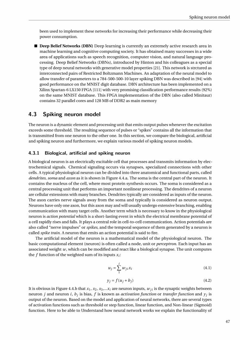
Spiking neuron model
been used to implement these networks for increasing their performance while decreasing theirpower consumption.
Deep Belief Networks (DBN) Deep learning is currently an extremely active research area inmachine learning and cognitive computing society. It has obtained many successes in a widearea of applications such as speech recognition, computer vision, and natural language pro-cessing. Deep Belief Networks (DBNs), introduced by Hinton and his colleagues as a specialtype of deep neural networks with generative model properties [21]. This network is strctured asinterconnected pairs of Restricted Boltzmann Machines. An adaptation of the neural model toallow transfer of parameters to a 784-500-500-10 layer spiking DBN was described in [94] withgood performance on the MNIST digit database. DBN architecture has been implemented on aXilinx Spartan-6 LX150 FPGA [111] with very promising classification performance results (92%)on the same MNIST database. This FPGA implementation of the DBN (also called Minitaur)contains 32 parallel cores and 128 MB of DDR2 as main memory
4.3 Spiking neuron modelThe neuron is a dynamic element and processing unit that emits output pulses whenever the excitationexceeds some threshold. The resulting sequence of pulses or “spikes” contains all the information thatis transmitted from one neuron to the other one. In this section, we compare the biological, artificialand spiking neuron and furthermore, we explain various model of spiking neuron models.
4.3.1 Biological, artificial and spiking neuronA biological neuron is an electrically excitable cell that processes and transmits information by elec-trochemical signals. Chemical signaling occurs via synapses, specialized connections with othercells. A typical physiological neuron can be divided into three anatomical and functional parts, calleddendrites, soma and axon as it is shown in Figure 4.4.a. The soma is the central part of the neuron. Itcontains the nucleus of the cell, where most protein synthesis occurs. The soma is considered as acentral processing unit that performs an important nonlinear processing. The dendrites of a neuronare cellular extensions with many branches. Dendrites typically are considered as inputs of the neuron.The axon carries nerve signals away from the soma and typically is considered as neuron output.Neurons have only one axon, but this axon may and will usually undergo extensive branching, enablingcommunication with many target cells. Another term which is necessary to know in the physiologicalneuron is action potential which is a short-lasting event in which the electrical membrane potential ofa cell rapidly rises and falls. It plays a central role in cell-to-cell communication. Action potentials arealso called “nerve impulses” or spikes, and the temporal sequence of them generated by a neuron iscalled spike train. A neuron that emits an action potential is said to fire.
The artificial model of the neuron is a mathematical model of the physiological neuron. Thebasic computational element (neuron) is often called a node, unit or perceptron. Each input has anassociated weight w , which can be modified and react like a biological synapse. The unit computesthe f function of the weighted sum of its inputs xi :
u j =i∑1
w j i xi (4.1)
y j = f (u j +b j ) (4.2)
It is obvious in Figure 4.4.b that x1, x2, x3,...xi are neuron inputs, w j i is the synaptic weights betweenneuron j and neuron i , b j is bias, f is known as activation function or transfer function and y j isoutput of the neuron. Based on the model and application of neural networks, there are several typesof activation functions such as threshold or step function, linear function, and Non-linear (Sigmoid)function. Here to be able to Understand how neural network works we explain the functionality of
47

CH4. NEUROMORPHIC COMPUTING IN SPIKING NEURAL NETWORK ARCHITECTURE
a:
b:
Inputs
SummationFunctions
x1
x2
x3
xi
wj1
wj2
wj3
wji
Σ
bj
Bias
yj
Output
ActivationFunctions
ujf(uj)
Soma
Synapse
Dendrites
Axon
Nucleus
Figure 4.4: The structure of a neuron a)Physiological neuron, b) Artificial neuron model.
neuron using threshold function. Respecting to the input connections in Figure 4.4.b, we can define athreshold for transfer function f by defining threshold θ. Here, we choose θ = 0 in the way we couldperform a binary classification.
y j =
1 if u j ≥ 00 if u j < 0
(4.3)
where u j is the induced local field of the neuron; which is,
u j =i∑1
w j i xi +b j (4.4)
Such a model of neuron is referred to McCulloch and Pitts [96].The Spiking neural model is an electrical model of physiological neuron that can be implemented
on the circuit using traditional devices or state-of-the-art technologies e.g., CMOS transistors or onhardware platforms e.g., FPGAs. In Spiking model the neurons communicate using spikes and theinput spikes make an action potential firing if inside a neuron reaches to the desired threshold (can becompared to threshold activation function in the artificial model of the neuron). Different models ofthe spiking neuron are proposed that here we study the main models.
Hodgkin-Huxley model
The first electrical model and in other words the first spiking model of neuron is Hodgkin-Huxleyneuron model [112] which got the Nobel Prize in Physiology or Medicine. Hodgkin and Huxley per-formed experiments on the giant axon of the squid and found three different types of current: sodium,potassium and leak current. It was demonstrated that the ionic permeability of the membrane can behighly dependent on the membrane potential. The schematic diagram of the Hodgkin-Huxley model isshown in Figure 4.5 where Er est is the membrane potential, C is the membrane capacitance, the leakagechannel is described by an independent R and the conductance of this leakage is calculated gL = 1
R theconductance the other ion channels (gN a = 1
RN aand gK = 1
RK) is voltage and time dependent. The ionic
48

Spiking neuron model
current is divided into components carried by sodium and potassium ions. Each element of the ioniccurrent is determined by a driving force which may easily be measured as an electrical potential, Er est
as resting membrane potential, EN a and EK sodium and potassium potentials respectively. Currentcan be carried through the membrane either by charging the membrane capacitance or by movingions through the resistances in parallel with the capacitance.
RK
I(t)
RNa
ErestENaEK
RLC RSYn
ErestEsyn
RL
synaptic connection
C
Figure 4.5: Electrical circuit represents Hodgkin-Haxley model of the neuron. a)Details circuit model ofthe neuron with sodium and potassium channels effects and leakage current, b) Equivalent circuit for moresimplicity in solving equations.
The equivalent circuit of Hodgkin-Hulxey model is shown in the left side of Figure 4.5 that byrepresenting the Krichhoffs law and using this circuit we can write following equations:
IL(t ) = VC (t )−Er est
RL(4.5)
Is yn(t ) =CdVC (t )
d t+ VC (t )−Er est
RL(4.6)
Solving the equation 4.6 leads to an exponential answer (Equation 4.7) that can model the behavior ofmembrane potential.
VC (t ) = v∞(1−exp(− t
τ)+Er est (4.7)
Respecting to the synaptic current charging if there is enough input current to membrane the neuronwill fire. We note that τ= RC in Equation 4.7 is the time constant for charging and discharging themembrane.
Integrate-and-Fire (I&F) neurons
Integrate-and-Fire (I&F) neuron model are derived from the Hodgkin-Huxley neuron model. Thereis an important type of I&F neuron model which is named Leaky-Integrate-and-Fire (LIF). There areother types of I&F models such as Quadratic-Integrate-and-Fire (QIF). The Leaky-Integrate-and-Fire(LIF) neuron model is a well-studied model of the neuron. There are three reasons for using LIF in ourplatform.
The fabricated model with recent CMOS technology is available [113, 114].
LIF works effectively in spiking and event-based networks [115].
LIF models are quite fast to simulate, and particularly attractive for large-scale network simula-tions [116].
Neurons integrate the spike inputs from other neurons they are connected to. These input spikeschange the internal potential of the neuron, it is known as neuron’s membrane potential or statevariable. When this membrane potential passes a threshold voltage due to integrated inputs, the action
49

CH4. NEUROMORPHIC COMPUTING IN SPIKING NEURAL NETWORK ARCHITECTURE
potential occurs, in other words, the neuron fires. The model is described by the neuron membranepotential:
τndv
dt=−v(t )+RIs yn(t ) (4.8)
Is yn(t ) =∑j
gi j∑nα(t − t (n)
j ) (4.9)
where, v(t) represents the membrane potential at time t, τn = RC is the membrane time constantand R is the membrane resistance. Equation 4.8 describes a simple parallel resistor-capacitor (RC)circuit where the leakage term is due to the resistor and the integration of Is yn(t ) is due to the capacitor.The total input current, Is yn(t ), is generated by the activity of pre-synaptic neurons. In fact, each pre-synaptic spike generates a post-synaptic current pulse. The total input current injected to a neuron isthe sum over all current pulses which is calculated in Equation 4.9. Time t (n)
j represents the time of thenth spike of post-synaptic neuron j , and gi j is the conductance of synaptic efficacy between neuroni and neuron j . Function α(t) = qδ(t), where q is the injected charge to the artificial synapse andδ(t ) is the Dirac pulse function. If Is yn(t ) is big enough where action potential can pass the thresholdvoltage, neuron fires. It means there are enough input spikes in a short time window. When there is noor only a few spikes in a time window, the neuron is in the leaky phase and the state variable decreasesexponentially. The duration of this time window depends on τn = RC . The equation is analyticallysolvable and thus we use the answer of Equation 4.8 in the network simulation when there is an inputspike to improve the simulation performance. In Figure 6.2, you can see the Matlab model of a singleneuron. When the input voltage passes the threshold, the neuron fires and resets to resting state. Themembrane potential stays for a definite period, which is called the refractory period, below the resetvalue.
Figure 4.6: Simulation of a single LIF neuron in Matlab, the input spikes are applied in t=[10, 30, 40,50] ms. Between 10 and 30 there is more decrease than between 30 and 40.
Izhikevich neuron model
Izhikevich neuron model [117] combines the biological plausibility of Hodgkin-Huxley model andthe computational efficiency of integrate-and-fire neurons. Using this model, we can simulate tensof thousands of spiking cortical neurons in real time. The model has two main characteristics it is
50

Synapse and learning
computationally simple as well as capable of producing rich firing patterns that physiological neuroncould produce.
dV (t )
dt= 0.04V (t )2 +5V (t )+140−u(t )+ I (t ) (4.10)
du(t )
dt= a.(b.V (t )−u(t )) (4.11)
ifV (t ) ≥ 30mV , then
V (t ) ← c
u(t ) ← u(t )+d(4.12)
Where V (t ) and u(t ) are variables without any dimension, and a, b, c, and d are parameters withoutdimension. V (t ) represents the membrane potential of the neuron and u(t ) represents a membranerecovery variable, which accounts for the activation of K + ionic currents and inactivation of N a+
ionic currents, and it provides negative feedback to V (t). Synaptic currents or injected dc-currentsare delivered via the variable I (t ). The parameter a describes the time scale of the recovery variableu(t ). Smaller value results in slower recovery. The parameter b presents the sensitivity of the recoveryvariable u(t ) to the subthreshold fluctuations of the membrane potential V (t ). Greater values coupleV (t ) and u(t ) more strongly resulting in possible subthreshold oscillations and low-threshold spikingdynamics. The parameter c represents the after-spike reset value of the membrane potential V (t)caused by the fast high-threshold K + conductances. Finally, the parameter d describes after-spikereset of the recovery variable u(t ) caused by slow high-threshold N a+ and K + conductance. Differentfiring behaviors can occur in biological spiking neurons and Izhikevich model can produce them isshown in Figure 4.7.
4.4 Synapse and learning
Synapse is a specialized structure with highly plastic characteristics enabling two neurons to exchangespike signals between themselves in other words, adjusting the connection strength between neurons.Thanks to the plasticity property of synapse, we can basically say the synapse is where the learninghappens in neural network system. A physiological synapse connects the axon of a presynaptic neuron(the neuron before the synapse) to the dendrite of a postsynaptic neuron (the neuron after the synapse).Two behavioral types of biological synapses are defined:chemical and electrical.
The chemical synapse is the primary definition of neurotransmitters between presynaptic andpostsynaptic neurons. A neurotransmitter through a chemical synapse consists of three parts. The axonpotential causes the presynaptic neuron to release a chemical substance into the synaptic cleft whichis an intracellular space between the two neurons. The neurotransmitter then diffuses through thesynaptic cleft. Moreover, the neurotransmitter causes a change in the voltage of the membrane of thepostsynaptic neuron. In biological neural system, a synapse is excitatory if the neurotransmitter causesan increase in the voltage of the postsynaptic neuron and inhibitory if it causes a reducing voltagein postsynaptic neuron. An electrical synapse consists of a group of gap junctions occurring closetogether. Gap junctions are tiny channels in the cell membrane that directly connect the cytoplasms oftwo cells [118]. The basic mechanism of synaptic transmission is well established. A presynaptic spikedepolarizes the synaptic terminal, leading to a calcium flow through presynaptic calcium channels,causing vesicles of neurotransmitter to be released into the synaptic cleft. The neurotransmitter bindstemporarily to postsynaptic channels, opening them and allowing ionic current to flow across themembrane. Modeling this complete electrochemical behavior is rather challenging. The purpose ofour study is not to model the exact behavior of synapse suitable for neuroscience study. The purposeof our study is to design a neuromorphic system appropriate for hardware implementation. Therefore,the behavior of synapse, neuron and model of neuron are studied to compare with recent techniquesin addition to recent alternative technologies for hardware implementations.
51

CH4. NEUROMORPHIC COMPUTING IN SPIKING NEURAL NETWORK ARCHITECTURE
Figure 4.7: Different Known types of neurons correspond to different values of the parameters a, b, c,and d could be reproduced by Izhikevich model From [117].
4.4.1 Synaptic learning and plasticity
To be able to model a proper synapse to contribute in learning process in an efficient way in neuralsystem, we need to analyze how learning happens in synapse. Neurons and synapses are the two basiccomputational units in the brain. The human brain consists of 1011 neurons and an extremely largenumber of synapses, 1015, which act as a highly complex interconnection network among the neurons.
Subsequently, each neuron is connected to 1000-10000 synapses [119]. Neuron computation isperformed by integrating the inputs coming from other neurons and producing spikes as based onvariety of the connections. The synapses contribute to the computation by modifying their connectionstrength as a result of neuronal activity, which is known as the synaptic plasticity. This synaptic
52

Synapse and learning
plasticity is believed as the basis of adaptation and learning, even in traditional neural network modelswhere several synaptic weight updating rules are based on Hebb’s law [120, 121].
Classes of learning algorithms
The primary significance of any type of neural networks is the property of learning from the envi-ronment to improve the performance of neural network. There are several types of learning algo-rithms.Although interconnection configuration of neural network is important in learning however,learning algorithms generally differ from each other in the way in which they adjust synapse weights.Simon Haykin, mentioned five different basic algorithms for learning in his book [106] namely memory-based, Hebbian, error-correction, competitive, and Boltzmann learning. Memory-based learningfunctionality is based on memorizing the training data explicitly. Hebbian and competitive learningare inspired by neurobiology. Error-correction is working using optimum filtering rule and Boltzmannlearning is based on ideas borrowed from statistical mechanics. In general, learning algorithms canbe divided into supervised or with teacher learning, semi-supervised learning, and unsupervised orwithout teacher learning algorithms (see Figure 4.8).
Supervised algorithmsTeacher has the knowledge of environment and this knowledge will be shared with the networkas some examples of inputs and their corresponding outputs. The supervision is continuedletting a modification rule adjust the synapses until the desired computation emerges as aconsequence of the training process. Then the supervision process is stopped and networkmust have the similar outputs with the specific inputs while the supervision was working. Error-correction algorithms which include the back-propagation using gradient descent is an exampleof supervised algorithms, other well-known supervised algorithms are support vector machines(SVM) and Bayesian type of learning algorithms. In fact, we put label on the data in training andcheck those labels in testing. This type of algorithms are used for regression and classifications.
Semi-supervised algorithmsSemi-supervised learning falls between supervised learning and unsupervised learning. Labeleddata are often difficult, expensive, and time consuming to obtain, as they require the efforts ofexperienced human annotators. Meanwhile unlabeled data may be relatively easy to collect.Semi-supervised uses large amount of unlabeled data, together with the labeled data, to buildbetter classifiers. Intuitively, in semi-supervised learning we can consider the learning problemas an exam and labeled data as the few example problems that the teacher solved in the course.The teacher also provides a set of unsolved problems. Semi-supervised learning requires lesshuman effort and gives higher accuracy, therefore it is of great interest both in theory and inpractical application.
Unsupervised algorithmsThere is no teacher and environment is unknown for the network too. There is no labeleddata output in unsupervised learning. Unsupervised learning can be thought of as findingpatterns in the data above and beyond what is considered as pure unstructured noise. One verysimple classic example of unsupervised learning is clustering. Hebbian plasticity is a form ofunsupervised learning, which is useful for clustering input data but less appropriate when adesired outcome for the network is known in advance.
Short-term and Long-term plasticity
Physiological synapses have an inherent dynamics, that controls how the pattern of amplitudes ofpostsynaptic responses depends on the temporal pattern of the incoming spike train. Indeed, eacheffective spike evokes a spike response in the postsynaptic neuron that is fewer (depression) or bigger(facilitation or potentiation) than the previous one. The strength of synaptic connections or weights are
53

CH4. NEUROMORPHIC COMPUTING IN SPIKING NEURAL NETWORK ARCHITECTURE
Learning Algorithms
Supervised Unsupervise
Semi-supervise
– Graph-Based Meth-ods
– Tree-Based Bayes
– Hebbian Learning
– Competitive Learn-ing
– Error-correction
– SVM
Figure 4.8: Different learning classifications.
caused by memorizing events, underling the ability of the brain to memorize. In the biological brain,short-term plasticity refers to a number of phenomena that affect the probability that a presynapticaction potential opens postsynaptic channels and that takes from milliseconds to tens of seconds.Short-term plasticity is achieved through the temporal enhancement of a synaptic connection, whichthen quickly decays to its initial state. Short-term plasticity depends on the sequence of presynapticspikes Figure 4.9.
Input sensory spike
Time
Mem
bran
e P
oten
tial
x(t)
t
Figure 4.9: Implementation of plasticity by local variables which each spike contributes to a trace x(t).The update of the trace depends on the sequence of presynaptic spikes
.
In local learning process, iteration of stimulation leads to a more stable change in the connectionto achieve long-term plasticity. Long-term plasticity is sensitive to the presynaptic firing rate over atime scale of tens or hundreds of seconds [122]. In general, synapses can exhibit potentiation anddepression over a variety of time scales, and multiple components of short- or long-term plasticity.Thus, four combination are possible from short and long term plasticity: Short-term potentiation (STP),short-term depression (STD), Long-term potantiation (LTP) and long-term depression (LTD) [123].
54

Synapse and learning
Spike-Timing Dependent Plasticity (STDP)
Most of the plasticity models employed in the neuroscience and neuromorphic approach were inspiredby Hebb’s (1949) postulate that explains the way that synapse connection weight should be modified:When an axon of cell A is near enough to excite cell B or repeatedly or persistently takes part in firing it,some growth process or metabolic change takes place in one or both cells such that A’s efficiency, as oneof the cells firing B, is increased.
Local learning rules aim to deal with information encoded by precise spike timing in local synapticmemory. One of the most commonly studied and used rules is spike-timing-dependent plasticity(STDP) [22, 23] that can be considered as a spike-based producing of Hebbian learning. Based on theSTDP modification rule, the synaptic changing is reinforced while both the pre- and post-synapticneurons are active, nothing prevents the synapses from strengthening themselves boundlessly, whichcauses the post-synaptic activity to explode [124] . Indeed, the plasticity depends on the time intervalsbetween pre- and postsynaptic spikes or in the other words, the concept of timing-LTP/LTD. The basicmechanisms of plasticity in STDP is derived from the long term potentiation (LTP) and the long termdepression (LTD). Pre-synaptic spikes that precede post-synaptic action potentials produce long-termpotentiation (LTP), and pre-synaptic spikes that proceed post-synaptic action potentials generatelong-term depression (LTD).
tjpre
tipost
i
Nj
tjpre tipost-0-30 30
Δwij
wij
Ni
-0.5
0.5
Δt
Figure 4.10: Basic of spike-timing-dependent plasticity. The STDP function expresses the change ofsynaptic weight as a function of the relative timing of pre- and post-synaptic spikes.
The basic configuration of STDP learning is depicted in Figure 4.10. The rate of weight changing∆w j i of a synapse from a presynaptic neuron j to postsynaptic neuron i depends on the relative timingbetween presynaptic spike and postsynaptic spikes. Let us name the presynaptic spike arrival timesat synapse j by t pr e
j where pr e = 1, 2, 3, ... counts the presynaptic spikes. Similarly, t posti with post =
1, 2, 3, ... labels the firing times of the postsynaptic neuron. The total weight change w j i induced byEquation 4.13 is then ( [22])
∆w =n∑
pr e=1
m∑post=1
W (x)(t posti − t pr e
j ) (4.13)
where W(x) is called a STDP learning function. Based on Zhang et al. [125] in their experimental work
55

CH4. NEUROMORPHIC COMPUTING IN SPIKING NEURAL NETWORK ARCHITECTURE
presented W(x) as:
W (x) =
A+e( −xτ+ ) if x ≥ 0
−A−e( xτ− ) if x < 0
(4.14)
where the parameters A+ and A− depend on the current value of the synaptic weight wi j . The timeconstants τ+ and τ− are on the order of 10 ms.
Different models for STDP learning
Multiple pre- or postsynaptic spikes occurring across a synapse in an interval of time, the plasticitymodification depends on their timing in a more complex manner. For instance, pair-based STDPmodels present “pre-post-pre” and “post-pre-pos” triplets of spikes with the same pairwise intervalsshould induce the same plasticity, however experimental studies demonstrated that these two tripletpatterns have different effects [126, 127].
Pair-based STDPIn this model of spike counting in the STDP interpret the biological evidence in terms of apair-based update rule, i.e. the modification of a synaptic weight depends on the temporaldifference between pairs of pre- and postsynaptic spikes:
Wi nc (x) = Fi nc (w).e(− |∆t |τ+ ) if ∆t > 0
Wdec (x) =−Fdec (w).e(− |∆t |τ− ) if ∆t < 0
(4.15)
In Equation 4.15,∆t = t posti −t pr e
j is the temporal difference between the post- and the presynap-tic spikes, and Fi nc (w)/Fdec (w) presents the dependence of the update on the current synapticweight. A pair-based model is fully specified by defining the form of Fi nc (w)/Fdec (w) as well asdetermining which pairs are taken into account to perform a new modification. A pair-basedweight modification rule can be implemented using two local variables: one for a low-passfiltered version of the presynaptic spike train and another one for the postsynaptic spike train asit is shown in Figure 4.11. Let us suppose that each spike from presynaptic neuron j contributesto a trace x j (t ) at the synapse weight then we can write:
d x j (t )
d t=−x j (t )
τpr e+ ∑
t pr ej
δ(t − t pr ej ) (4.16)
where t pr ej represents the history of the firing times of the presynaptic neuron. In particular, the
variable is increased by an amount of one at the arrival time of a presynaptic spike and reducesexponentially with time constant τpr e afterwards. Similarly, each spike from postsynaptic neuroni contributes to a trace xi (t ):
d xi (t )
d t=− xi (t )
τpost+ ∑
t posti
δ(t − t posti ) (4.17)
where t posti presents the firing times of the postsynaptic neuron. Similar to presynaptic spike, a
decrease of the weight is induced proportionally to the momentary value of the postsynaptictrace xi (t). The steady-state average for synaptic strength in pair-based STDP has a stablenontrivial mean if the depression window is larger than the potentiation window [127]. Thisfixed point is unique, so the mean of the steady-state distribution of synaptic weights convergesto this value regardless of its initial value. The stability of the mean is not a sufficient conditionfor the steady-state distribution of synaptic strengths to be fully stable, each synapse mustalso have a stable deviation from the mean. The connection strength of a particular synapsecan be presented as w = w +δw , where δw is the deviation of the synapse from the mean. Ifthe deviation is going to grow over time, the synapses will drift away from the mean and thedistribution will be partially stable. If the deviation tends to decrease, the synapses will clusteraround the mean and the distribution will be stable.
56

Synapse and learning
xj(t)
Pre
Post
xi(t)
trace of Presynaptic spike
trace of postsynaptic spike
Wji(t)
Figure 4.11: Pair-based STDP using local variables. The spikes of presynaptic neuron j leave a tracex j (t ) and the spikes of the postsynaptic neuron i leave a trace xi (t ). The update of the weight W j i at themoment of a postsynaptic spike is proportional to the momentary value of the trace x j (t ) (filled circles).This gives the amount of potentiation due to pre-before-post pairings. Analogously, the update of W j i
on the occurrence of a presynaptic spike is proportional to the momentary value of the trace xi (t)(unfilled circles), which gives the amount of depression due to post-before-pre pairings
The triplet modelThe standard pair-based STDP models predict that if the repetition frequency is increased, thestrength of the depressing interaction becomes greater, leading to less network potentiation. Thefrequency-dependence of STDP experiments can be accounted for if one assumes that the basicbuilding block of potentiation during STDP experiments is not only a pair-wise interaction butalso could be a triplet interaction between two postsynaptic spikes and one presynaptic spike.Pfister & Gerstner [128] to propose the triplet model, which takes into account interactions ofspikes beyond pre-post pairings. This model is based on sets of three spikes, one presynaptic andtwo postsynaptic. For a pre-post-pre triplet, the first presynaptic spike enforces extra depressionon the synapse, additionally for a post-pre-post triplet the first postsynaptic spike enforces extrapotentiation. The triplet model sums the contributions of all previous pre- and postsynapticspikes as well as all pre-post pairings. Pfister & Gerstner [128] also provided a version of thetriplet model based only on nearest neighboring spikes, but the qualitative behavior of both allto all and nearest neighboring versions is similar.
Similarly to pair-based rules, each spike from presynaptic neuron j contributes to a trace x j (t ) atthe synapse:
d x j (t )
d t=−x j (t )
τpr e+ ∑
t pr ej
δ(t − t pr ej ) (4.18)
where t pr ej presents the firing times of the presynaptic neuron. In contrast with pair-based STDP,
each spike from postsynaptic neuron i contributes to a fast trace xi (t ) and a slow trace x ′i (t ) at
the synapse:d xi (t )
d t=− xi (t )
τ1post+ ∑
t posti
δ(t − t posti ) (4.19)
d x ′i (t )
d t=− x ′
i (t )
τ2post+ ∑
t posti
δ(t − t posti ) (4.20)
57

CH4. NEUROMORPHIC COMPUTING IN SPIKING NEURAL NETWORK ARCHITECTURE
where τ1post < τ2post , how the triplet model works is depicted in Figure 4.12. In this model,LTD is induced as in the standard STDP pair model in Equation 4.15, i.e. the weight changeis proportional to the value of the fast postsynaptic trace xi (t) evaluated at the arrival of apresynaptic spike. The new feature of the rule is that LTP is pursued by a triplet effect: the weightchange is proportional to the value of the presynaptic trace x j (t ) evaluated at the arrival time of apostsynaptic spike as well as to the slow postsynaptic trace x ′
i (t ) from previous postsynaptic spike.The main functional advantage of a triplet STDP rule is that it can be mapped to a Bienenstock-
xj(t)
Pre
Post
xi(t)
trace of Presynaptic spike
trace of postsynaptic spikes
x'i(t)
Figure 4.12: Triplet STDP model using local variables. The spikes of presynaptic neuron j contribute toa trace x j (t ), the spikes of postsynaptic neuron i contribute to a fast trace xi (t ) and a slow trace x ′
i (t ).The update of the weight W j i at the arrival of a presynaptic spike is proportional value of the fast tracexi (t ) (green unfilled circles), as in the pair-based model. The update of the weight W j i at the arrival ofa postsynaptic spike is proportional to the value of the trace x j (t ) (red filled circles) and the value ofthe slow trace x ′
i (t ) just before the spike (green filled circles).
Cooper-Munro learning rule [129]. It means if we assume that the pre- and postsynaptic spiketrains are managed by Poisson statistics, the triplet rule presents depression for low postsynapticfiring rates and potentiation for high postsynaptic firing rates.
Suppression modelPlasticity experiments using triplets of spikes demonstrated different effects than the hippocam-pal results. In the synapses of the visual cortex of rats, pre-post-pre triplets induce potentiationwhile post-pre-post triplets induce depression. These results led Froemke et al. [130] to developthe suppression model, in which STDP is induced by nearest neighbor pre- and postsynapticspikes. In this model of STDP, the plasticity is computed from the standard pair-based STDPcurve, however the impact of the presynaptic spike in each pair is suppressed by previous presy-naptic spikes and, similarly, the plasticity induced by the postsynaptic spike in each pair issuppressed by previous postsynaptic spikes as it is shown in Figure 4.13.
The suppression is maximal after each pre- or postsynaptic spike, and it decreases exponentiallyas the interval between consecutive pre- or postsynaptic spike increases. In a post-pre-postsequence of spikes, the timing of the first post-pre pairing was the best predictor for the synapticweight modification. Moreover, in a pre-post-pre sequence of spikes, the first pre-post pair
58

Synapse and learning
Figure 4.13: The suppression STDP model. A) Spike interactions in the suppression model, in which theimpact of the presynaptic spike in a pair is suppressed by a previous presynaptic spike (top), and theimpact of the postsynaptic spike is suppressed by a previous postsynaptic spike (bottom). B) Plasticityin the suppression model induced by triplets of spikes: pre-post-pre triplets induce potentiation (topleft), and post-pre-post triplets induce depression (bottom right), From [127].
induces potentiation, nevertheless the amount of depression induced by the second post-prepair is suppressed by the first presynaptic spike. In the suppression STDP model, synaptic weightmodification is presented by
∆w = (1−e− ∆tpr e
τpr e )(1−e− ∆tpost
τpost )×
Ai nc .e(− ∆t
τi nc ) if ∆t ≥ 0
−Adec .e( ∆tτdec ) if ∆t < 0
(4.21)
where ∆tpr e is the interval between the presynaptic spike in the pair and its preceding presy-naptic spike, and ∆tpost is the interval between the postsynaptic spike and its preceding spike.This model introduces a proper fit to triplet and quadruplet protocols particularly in the visualcortex, and also represents a much better prediction for synaptic changing due to natural spiketrains [130]. Nonetheless, it does not predict the increase of LTP with the repetition frequency.
Voltage dependence modelExperimental model of Spike-Timing Dependent Plasticity recommends that synaptic weightmodifications are caused by the tight temporal correlations between pre- and post- synapticspikes. However, other experimental protocols where presynaptic spikes are paired with a fixeddepolarization of the postsynaptic neuron (e.g. under voltage clamp) show that postsynapticspikes are not necessary to induce long-term potentiation and depression of the synapse [131].
It has been discussed whether the voltage dependence is more fundamental than the depen-dence on postsynaptic spike. In fact, voltage dependence alone can produce a behavior similarto STDP learning, as the membrane potential reacts in a particular manner in the vicinity of aspike it means high shortly before a spike, and low shortly after. Alternatively, a dependence onthe slope of the postsynaptic membrane potential has been shown to regenerate the propertiesof STDP weight change curve. The voltage effects caused by back-propagating spikes is implicitlycontained in the mechanistic formulation of STDP models outlined above. In particular, thefast postsynaptic trace xi (t) in the triplet model can be considered as an approximation of abackpropagating action potential. In contrast, a standalone STDP rule does not automaticallygenerate a voltage dependence. Furthermore, synaptic effects caused by subthreshold depo-larization in the absence of postsynaptic firing cannot be modeled by standard STDP or tripletmodels.
The NMDAR-based modelThe NMDAR-based model was proposed for the first time in [132] and “NMDAR-based model”,
59
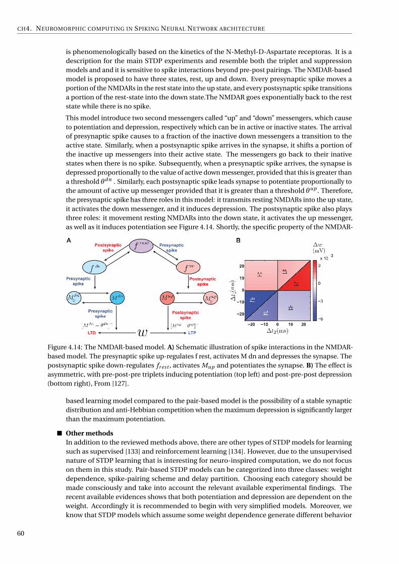
CH4. NEUROMORPHIC COMPUTING IN SPIKING NEURAL NETWORK ARCHITECTURE
is phenomenologically based on the kinetics of the N-Methyl-D-Aspartate receptoras. It is adescription for the main STDP experiments and resemble both the triplet and suppressionmodels and and it is sensitive to spike interactions beyond pre-post pairings. The NMDAR-basedmodel is proposed to have three states, rest, up and down. Every presynaptic spike moves aportion of the NMDARs in the rest state into the up state, and every postsynaptic spike transitionsa portion of the rest-state into the down state.The NMDAR goes exponentially back to the reststate while there is no spike.
This model introduce two second messengers called “up” and “down” messengers, which causeto potentiation and depression, respectively which can be in active or inactive states. The arrivalof presynaptic spike causes to a fraction of the inactive down messengers a transition to theactive state. Similarly, when a postsynaptic spike arrives in the synapse, it shifts a portion ofthe inactive up messengers into their active state. The messengers go back to their inativestates when there is no spike. Subsequently, when a presynaptic spike arrives, the synapse isdepressed proportionally to the value of active down messenger, provided that this is greater thana threshold θdn . Similarly, each postsynaptic spike leads synapse to potentiate proportionally tothe amount of active up messenger provided that it is greater than a threshold θup . Therefore,the presynaptic spike has three roles in this model: it transmits resting NMDARs into the up state,it activates the down messenger, and it induces depression. The postsynaptic spike also playsthree roles: it movement resting NMDARs into the down state, it activates the up messenger,as well as it induces potentiation see Figure 4.14. Shortly, the specific property of the NMDAR-
Figure 4.14: The NMDAR-based model. A) Schematic illustration of spike interactions in the NMDAR-based model. The presynaptic spike up-regulates f rest, activates M dn and depresses the synapse. Thepostsynaptic spike down-regulates fr est , activates Mup and potentiates the synapse. B) The effect isasymmetric, with pre-post-pre triplets inducing potentiation (top left) and post-pre-post depression(bottom right), From [127].
based learning model compared to the pair-based model is the possibility of a stable synapticdistribution and anti-Hebbian competition when the maximum depression is significantly largerthan the maximum potentiation.
Other methodsIn addition to the reviewed methods above, there are other types of STDP models for learningsuch as supervised [133] and reinforcement learning [134]. However, due to the unsupervisednature of STDP learning that is interesting for neuro-inspired computation, we do not focuson them in this study. Pair-based STDP models can be categorized into three classes: weightdependence, spike-pairing scheme and delay partition. Choosing each category should bemade consciously and take into account the relevant available experimental findings. Therecent available evidences shows that both potentiation and depression are dependent on theweight. Accordingly it is recommended to begin with very simplified models. Moreover, weknow that STDP models which assume some weight dependence generate different behavior
60

Hardware spiking neural network systems
from the additive model. The pair-based and triplet models are partially stable and use Hebbiancompetition. The Suppression and NMDAR-based have more stability but they use anti-Hebbiancompetition. The main challenge in this domain is to perform analytical and simulation studiesthat are able to identify and characterize their composite effects, and investigate their functionalconsequences.
4.5 Hardware spiking neural network systemsSpecific application domains such as Big Data classification, visual processing, pattern recognitionand in general sensory input data, require information processing systems which are able to classifythe data and to learn from the patterns in the data. Such systems should be power-efficient. Thusresearchers have developed brain-inspired architectures such as spiking neural networks. For largescale brain-like computing on neuromorphic hardware, there are four approaches:
1. Microprocessor based approaches where the system can read the codes to execute and modelthe behavior of neural systems and cognitive computation such as the SpiNNaker machine [29].
2. Fully digital custom circuits where the neural system components are modeled in circuit usingstate-of-the-art CMOS technology e.g., IBM TrueNorth machine [18].
3. Analog/digital mixed-signal systems that model the behavior of biological neural systems, e.g.the NeuroGrid [30] and BrainScales [31] projects.
4. Memristor crossbar array based systems where the analog behavior of the memristors emulatethe synapses of a spiking neural network.
In the following, we give some details about these approaches and compare their performance.SpiNNaker is a massively parallel and processor-based (ARM processor) system with the purpose of
building large scale spiking neural networks simulations. It is highly scalable and capable to simulatea network from thousands to millions of neurons with varying degree of connectivity. It proposes tointegrate 57,600 custom VLSI chips based on the AER (Address Event Representation) communicationprotocol [135]. Each chip contains 18 fixed-point advanced RISC ARM968 processing cores next to thecustom routing infrastructure circuits which is dedicated 96 kB of local memory besides 128 MB ofshared Dynamic Random Access Memory (DRAM) as it is depicted in Figure 4.15.a. The router memoryconsists of a three-state 1024×32 bits Content Addressable Memory (CAM) and a 1024×24 bits RandomAccess Memory (RAM). Going more to the details, each ARM core has a local 32 kB instruction memoryand 64 kB data memory. Regarding to the architecture and design properties, SpiNNaker offers veryfast simulation of large scale neural networks. It has a remarkable flexibility for arbitrary connectivityfor network architecture and various neurons, synapses and learning algorithms. However, the systemstill uses von Neumann architecture with a large extent of memory hierarchies found in conventionalcomputers with memory wall bottleneck issues. Although using low-power ARM processors dedicatedto power-efficient platforms used in training and robotic applications with four to 48 nodes, SpiNNakerconsumes a relatively small amount of power. However, the largest machine with the ability to simulateof one percent of a human brain and incorporating over a million ARM processor cores, still requiresup to 75 kW of electrical power.
IBM designed a scalable, flexible and non-von Neumann full custom spiking neural networknamed “TrueNorth”. Although TrueNorth uses transistors as digital gates, they use event-drivenmethod to communicate in fully asynchronous manner. The structure of TrueNorth consists of 5.4billion transistors to build 4096 neurosynaptic cores. Each core includes 256 digital LIF neurons,256×256 binary programmable synapses, and asynchronous encoding/decoding and routing circuits.Each synapse has a binary behavior that can be individually turned on or off and can be assignedto model one type of inhibitory and two types of excitatory synapse with different weights. Neurondynamics has a global 1 kHz clock and so is discretized into 1 ms time steps. Regarding to the synaptic
61

CH4. NEUROMORPHIC COMPUTING IN SPIKING NEURAL NETWORK ARCHITECTURE
matrix, each neuron can be connected to one up to 256 neurons of a destination core. The routing inTrueNorth is less flexible than in SpiNNaker, however TrueNorth can distribute the system memoryincludes core synaptic matrix and routing table entries (Figure 4.15.b) The architecture thus supportsdynamics of connectivity that includes feed-forward, recurrent, and lateral connections. The powerconsumption is 20 mW/cm2, though the traditional central processing unit (CPU) is 50 to 100 W/cm2.In this platform the synapses do not implement any plasticity mechanism, therefore they are not ableto perform on-line learning.
The BrainScales project (Brain-inspired multiscale computation in neuromorphic hybrid systems)is the successor of FACETS [136] project. This project proposes the design and implementation ofa custom analog/digital mixed-signal simulation engine that is able to implement the differentialequations with an acceptable accuracy. This computational neuroscience model is provided by neuro-scientists, and reproduces the results obtained from numerical simulations executed on conventionalcomputers. The Heidelberg University BrainScales project (HICANN chip) aims to produce a wafer-scale neural simulation platform, in which each 8 inch silicon wafer integrates 50×106 plastic synapsesand 200,000 biologically realistic neuron circuits (see Figure 4.15.c). In order to have a scalable sizewith maximum number of processors on the wafer, relatively small capacitors have been applied formodeling the synapses and neurons. Accordingly, using the large currents generated by the above-threshold circuit and the small capacitors, the BrainScales circuits are not able to achieve the longtime-constants required for interacting with real-time environments. However, the speed of networkcomponents operations compared to biological elements reactions is accelerated by a factor of 103 or104 which can reduce the simulation time dramatically. Furthermore, it needs large bandwidth andfast switching and still high-power circuit for propagating spikes across the network [4].
NeuroGrid is another big project developed at Stanford University that emulates neuromorphicengineering vision, sub-threshold network components circuits and uses analog/digital mixed-signalto model continuous time for network elements. This meuromorphic platform simulates a millionneurons with billions of synaptic connections in real-time. Such as TrueNorth and BrainScales thearchitecture of Neurogrid is non-von Neumann. Neurogrid emulates four network elements: axon,dendrite, soma and synapse. Only the axon circuit is digital and the other elements are modeledin the analog circuits due to the better energy efficiency. NeuroGrid consists of 16 standard CMOS“NeuroCores” (see Figure 4.15.d) integrated on a board that works using 3 W of power energy connectedin a tree network, with each NeuroCore consisting of a 256×256 array of two-compartmental neurons.The synaptic circuits are shared among the neurons while different spikes can be assigned to thesame synapse. The main goal of neuromorphic systems is to interact with real physical environmentsand process the natural signals with physiological time-scales, Neurogrid has long time constants inthe range of tens of milliseconds. Consequently, this long time constants limitation causes difficultyin using typical VLSI for design and implementation. Neurogrid and BrainScales similarly use thetemporal dynamic of memory elements to store the state of the network. Accordingly, these twoprojects have the capability of local learning using the STDP learning rule.
An alternative to these architectures, that has been proposed by several authors [7, 9, 39, 43, 137], isto use memristive devices as synapses in neuromorphic circuits. This has the potential to lower theenergy consumption by a large proportion. It has also been showed that the memristors can emulatethe STDP learning rule, and thus lead to unsupervised learning circuits. We have thus chosen to studythis kind of architecture and, in particular, to check how some parameters of the architecture or of thedevices influence the learning capabilities of the circuit.
4.6 Discussion
Still for a network simulation and implementation of neuromorphic spiking system, we need moretechniques such as homeostasis and lateral inhibition to support learning process for an optimizedsystem. Homeostasis is used in the SNN to adapt the threshold level of neurons to learning in SNN.Another consideration is lateral inhibition while we are using unsupervised learning methods such as
62
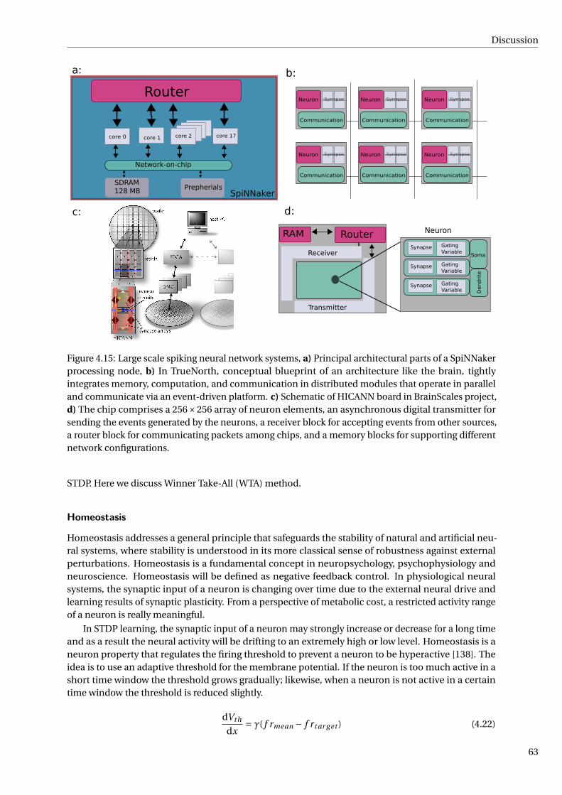
Discussion
core 0
SpiNNaker
a: b:
Router
core 1 core 2 core 17
Network-on-chip
SDRAM128 MB Prepherials
Neuron Synapse
Communication
Neuron Synapse
Communication
Neuron Synapse
Communication
Neuron Synapse
Communication
Neuron Synapse
Communication
Neuron Synapse
Communication
c:
RAM Router
Transmitter
ReceiverSynapse Gating
VariableSoma
Synapse GatingVariable
Synapse GatingVariable D
endri
te
Neuron
d:
Figure 4.15: Large scale spiking neural network systems, a) Principal architectural parts of a SpiNNakerprocessing node, b) In TrueNorth, conceptual blueprint of an architecture like the brain, tightlyintegrates memory, computation, and communication in distributed modules that operate in paralleland communicate via an event-driven platform. c) Schematic of HICANN board in BrainScales project,d) The chip comprises a 256×256 array of neuron elements, an asynchronous digital transmitter forsending the events generated by the neurons, a receiver block for accepting events from other sources,a router block for communicating packets among chips, and a memory blocks for supporting differentnetwork configurations.
STDP. Here we discuss Winner Take-All (WTA) method.
Homeostasis
Homeostasis addresses a general principle that safeguards the stability of natural and artificial neu-ral systems, where stability is understood in its more classical sense of robustness against externalperturbations. Homeostasis is a fundamental concept in neuropsychology, psychophysiology andneuroscience. Homeostasis will be defined as negative feedback control. In physiological neuralsystems, the synaptic input of a neuron is changing over time due to the external neural drive andlearning results of synaptic plasticity. From a perspective of metabolic cost, a restricted activity rangeof a neuron is really meaningful.
In STDP learning, the synaptic input of a neuron may strongly increase or decrease for a long timeand as a result the neural activity will be drifting to an extremely high or low level. Homeostasis is aneuron property that regulates the firing threshold to prevent a neuron to be hyperactive [138]. Theidea is to use an adaptive threshold for the membrane potential. If the neuron is too much active in ashort time window the threshold grows gradually; likewise, when a neuron is not active in a certaintime window the threshold is reduced slightly.
dVth
dx= γ( f rmean − f rt ar g et ) (4.22)
63

CH4. NEUROMORPHIC COMPUTING IN SPIKING NEURAL NETWORK ARCHITECTURE
where f rmean is the mean activity (or firing rate) of a neuron, f rt ar g et is the target activity, and γ is amultiplicative positive constant. Consequently, the activity of the neuron is bounded in a homeostaticrange to encode the synaptic input more effectively to improve the STDP learning [139].
Winner-take-all
In a winner-take-all (WTA) network, in output layer or partially output layers, neurons competewith each other based on their output activities, which leads to an adaptation only of the weights ofthe neuron with the highest output activity [140]. In unsupervised learning using spike coding andplasticity learning. Without competition, all the neurons would behave alike and no specializationtakes place in the neurons. The theoretical analysis shows that winner-take-all is a surprisingly powerfulcomputational method compared with threshold gate (McCulloch-Pitts neuron) and sigmoidal gate[141]. There have been many implementations of winner take all (WTA) computations in recurrentnetworks in the literature [24, 25]. Also there have been many analog VLSI implementations of thesecircuit [25,142]. In WTA, after the competition, only one neuron will be the most active for some inputsand the rest of the neurons will eventually become inactive for those inputs. Physiologically plausiblelearning methods can be mainly classified as dense, local, or sparse. Competitive learning such asWTA is a local learning rule as it activates only the unit that fits the input pattern best and suppressesthe others through fixed inhibitory connections.
The simplest competitive computational model is a hard WTA that computes a function fW T A :Rn →0,1n whose output ⟨b1, ...,bn⟩ = fW T A(x1, ..., xn) satisfies
bi =
1 if xi > x j for all j 6= i0 if xi < x j for some j 6= i
(4.23)
Therefore in the case of inputs x1, ..., xn a single output bi has values 1 that marks the position ofthe biggest input xi . Wolfgang Maass [141] introduced two types of WTA namely k-WTA and soft-WTA.In k-WTA, bi has value 1 if and only if xi is among the k largest inputs. In soft-WTA the ith output is ananalog variable ri whose value reflects the rank of xi among the input variables. We use WTA in ourresearch that will be presented in the next sections.
4.7 ConclusionNeuromorphic computation using Spiking Neural Networks (SNN) is proposed as an alternativesolution for future of computation to conquer the memory bottelneck issue in recent computerarchitecture. Different spike codings have been discussed to improve data transferring and dataprocessing in neuro-inspired computation paradigms. Choosing the appropriate neural networktopology could result in better performance of computation, recognition and classification. Themodel of the neuron is another important factor to design and implement SNN systems. The speedof simulation and implementation, ability of integration to the other elements of the network, andsuitability for scalable networks are the factors to select a neuron model. The learning algorithms aresignificant consideration to train the neural network for weight modification. As the most frequentused unsupervised method for network training in SNN is STDP, we analyzed and reviewed the variousmethods of STDP. Furthermore, in the next chapters, we use STDP as the main learning algorithm totrain the network. The sequential order of pre- or postsynaptic spikes occurring across a synapse in aninterval of time leads to defining different STDP methods. Based on the importance of stability as wellas Hebbian competition or anti-Hebbian competition the method will be used in weight modification.To step further more confidently in next part of our work, we surveyed the most significant projectsthat cause making neuromorphic platform. The advantages and disadvantages of each neuromorphicplatform have been introduced in this chapter.
64

Part II
Our contribution in spiking neuralnetwork architecture: Simulator, New
synapse box, Parameter exploration andSpiking deep learning
65


Chapter 5
N2S3, an Open-Source Scalable SpikingNeuromorphic Hardware Simulator
Abstract
One of the most promising approaches to overcome the end of Moore’s law is neuromorphiccomputing. Indeed, neural networks already have a great impact on machine learning applicationsand offer very nice properties to cope with the problems of nanoelectronics manufacturing, suchas a good tolerance to device variability and circuit defects, and a low activity, leading to lowenergy consumption. We present here N2S3 (for Neural Network Scalable Spiking Simulator), anopen-source simulator that is built to help design spiking neuromorphic circuits based on nano-electronics. N2S3 is an event-based simulator and its main properties are flexibility, extensibility,and scalability. One of our goals with the release of N2S3 as open-source software is to promote thereproducibility of research on neuromorphic hardware. We designed N2S3 to be used as a library,to be easily extended with new models and to provide a user-friendly special purpose language todescribe the simulations.
5.1 IntroductionNeuromorphic computing is a suitable alternative for conventional computation to take the advantagesof low power computing for future computer architectures [18]. In fact, parallel neuro-inspiredcomputing, by performing computation and storage on the same devices, can overcome the vonNeumann bottleneck. Several large projects are based on neuromorphic systems, such as the EUHuman Brain Project [143], the DARPA/IBM SYNAPSE project [144], and deep learning research led byGoogle and Facebook, among others.
Recently, emerging nano-scale devices have demonstrated novel properties for producing newmemories and unconventional processing units. One of those is the memristor, that was hypotheticallypresented by Leon Chua in 1971 [6]; after a few decades, HP was the first to announce a successfulmemristor fabrication [2]. The unique properties of memristors, such as extreme scalability, flexibilitythanks to their analog behavior, and their ability to remember their last state, make memristors verypromising candidates to be used as synapses in Spiking Neural Networks (SNN) [7].
Given their potential of very low power execution and their capability to handle natural signals,we focus on SNN. A comprehensive introduction and literature review about SNN was published byPaugam-Moisy and Bohte in 2012 [145]. The authors explore the computational capabilities of SNN,their learning capabilities, and their simulation.
Brette et al. [116] surveyed and discussed the existing work on SNN simulation in 2007. All thesimulators discussed in this chapter as well as the more recent Brian [146] target the simulation of bio-logical SNN. More recently, Bichler et al. [32] proposed Xnet, a C++ event-driven simulator dedicated tothe simulation of hardware SNN. In our work, we share the goals of Xnet: “intermediate modeling level,
67
CH5. N2S3, AN OPEN-SOURCE SCALABLE SPIKING NEUROMORPHIC HARDWARE SIMULATOR
between low-level hardware description languages and high-level neural networks simulators usedprimarily in neurosciences”, and “the integration of synaptic memristive device modeling, hardwareconstraints and any custom features required for the targeted application”. In addition to these goals,we put an emphasis on flexibility and usability to allow the study of various kinds of hardware designs(possibly by other researchers than us), scalability to simulate large hardware SNNs, and softwareengineering best practices (robust and extensible software architecture for maintainability, extensivetest suite, continuous integration, open-source distribution).
Figure 5.1:N2S3 Logo
In this chapter we present N2S3 (Neural Network Scalable Spiking Simulator,pronounced “Nessie”, hence its logo), an event-driven simulator dedicated to theexploration of hardware SNN architectures [147]. The internals of N2S3 are basedon the exchanges of messages between concurrent actors [148], mimicking theexchange of spikes between neurons. N2S3 has been developed from the groundup for extensibility, allowing to model various kinds of neuron and synapse models,various network topologies (especially, it is not restricted to feed-forward networks),various learning procedures, various reporting facilities, and to be user-friendly, witha domain specific language to easily express and run new experiments. It is available as open-sourcesoftware at https://sourcesup.renater.fr/wiki/n2s3 so that its users can share their modelsand experimental settings to enable others to reproduce their results. In this spirit, N2S3 is distributedwith the implementation of two “classical” experiments: handwritten digit recognition on the MNISTdataset [20, 26] and the highway vehicle counting experiment [27].
In the remainder of this chapter, we will first detail the fundamental architectural choices of N2S3,then the models that are already implemented in N2S3, and finally the features that N2S3 provides toimplement and run experiments.
5.2 Event-Driven Simulation Architecture
5.2.1 Event-Driven vs Clock-Driven Simulation
SNN are essentially defined by standard differential equations, but because of the discontinuitiescaused by the spikes, designing an efficient simulation of spiking neural networks is a non-trivialproblem. There are two families of simulation algorithms: event-based simulators and clock-basedones. Synchronous or “clock-driven” simulation simultaneously updates all the neurons at every tickof a clock, and is easier to code, especially on GPUs, for getting an efficient execution of data-parallellearning algorithms. Event-driven simulation behaves more like hardware, in which conceptuallyconcurrent components are activated by incoming signals (or events).
Event-driven execution is particularly suitable for untethered devices such as neurons and synapses,since the nodes can be put into a sleep mode to preserve energy when no interesting event is hap-pening. Energy-aware simulation needs information about active hardware units and event countersto establish the energy usage of each spike and each component of the neural network. Further-more, as the learning mechanisms of spiking neural networks are based on the timings of spikes, thechoice of the clock period for a clock-based simulation may lead either to imprecision or to a highercomputational cost.
There is also a fundamental gap between this event-driven execution model and the clock-basedone: the first one is independent on the hardware architecture of computers on which it is running. So,event-driven simulators can naturally run on a grid of computers, with the caveat of synchronizationissues in the management of event timings.
5.2.2 Technological Choices: Scala and Akka
To address our concurrency and distributability requirements (i.e., ability to scale out a simulationon several computers to handle large networks) we have chosen to use the Scala programming lan-guage [149] along with the Akka actor library [148].
68

Neuron, Synapse, Network Modeling
5.2.3 Software ArchitectureThe architecture of N2S3 is organized in Akka actors. Our choice for an actor model aims mainly forthe distribution and scalability of large neural networks. Each entity of the simulation is deployed in aconcrete actor that is assigned to a concrete machine at runtime. The core of a typical neural networksimulation in N2S3 is composed mainly by the following network entities:
Containers Containers are network entities in charge of organizing the network structure. Theirmain responsibility is to contain network entities and dispatch messages to their children.
Neurons The basic building blocks of a neural network. In N2S3, a neuron is composed of both itsnucleus (the soma) and its incoming connections (dentrites and associated synapses).
Each N2S3 actor has a network container capable of containing one or multiple entities. Thisparticularity allows us to control how distribution and parallelism is managed in each simulation.Figure 5.2 illustrates the architecture with an example network. In this figure, the simulation is madeof one input and a neural network organized in two layers. The input of the simulation resides in oneactor, the hidden layer is split in one actor per neuron, and all neurons of the output layer reside in asingle actor. The reason why one would put several neurons in the same or a different actor is basedon the scalability and the synchronization choices for the experiment. The topology of the network(discussed in more details in Section 5.3.3) is one of the major influence on these questions.
The communication between simulation entities requires to identify each object by a URI madeof a pair (actor, local_identifier). The component actor is the Akka actor that contains theentity and local_identifier is a path that identifies each object uniquely within its actor.
Since actors are inherently concurrent, one concern is how the temporal order of messages isguaranteed during the simulation. To do so, N2S3 allows to configure several levels of synchronizationto be used by the simulation designer. On one end of the spectrum, N2S3 may make use of a uniquesynchronizer for the simulation, which will ensure that no causality issues happen but can create abottleneck that will affect the performance of the simulation. On the other end of the spectrum, wecan also configure N2S3 to use a synchronization mechanism which is local to each neuron. The latterpolicy enables better parallelism, but may cause some temporal consistency problems.
5.3 Neuron, Synapse, Network Modeling
5.3.1 Neuron ModelingThe neuron is a dynamic element and processing unit that emits output pulses whenever the excitationexceeds some threshold. The resulting sequence of pulses or spikes contains all the information that istransmitted from one neuron to another one. As we have chosen event-driven simulation, the state ofa neuron is updated only when an event representing a spike is received.
We provide by default a Leaky-Integrate-and-Fire (LIF) neuron model [115]. There are severalreasons for using a LIF model:
CMOS technology fabrication of this model is available [113, 114];
it is fast enough to simulate, and in particular it is effective for large-scale network simula-tions [116].
In LIF, neurons integrate the spikes coming from other neurons. These spikes can change theinternal potential of the neuron, which is known as the membrane potential or state variable of theneuron. When the membrane potential reaches a given threshold voltage after integrating enoughinput spikes, an action potential occurs; in other words, the neuron fires, generating an output spike.This is done by updating the membrane potential using the value computed when receiving the lastspike and the analytical solution to the differential equations defining the behavior of the LIF neuron.
69

CH5. N2S3, AN OPEN-SOURCE SCALABLE SPIKING NEUROMORPHIC HARDWARE SIMULATOR
Figure 5.2: N2S3 Architecture. A network is organized in actors that may contain one or more networkentities. Such entities could be for example, neurons, inputs or any other.
In order to improve the learning capabilities of neural networks, we provide two refinements ofthe neuron model: homeostasis and a refractory period. Homeostasis [138] dynamically adapts thethreshold of each neuron to the activity of this neuron to prevent a neuron from being over-active orinactive. To allow more specialization of the neurons, we include a refractory period after the firing ofa neuron during which it ignores incoming spikes.
5.3.2 Synapse modeling and learning
A synapse operates as a plastic controller between two neurons. This plasticity is believed to be theorigin of the learning and memorization capabilities of the brain [150]. Hence, hardware spiking neuralnetworks usually use some kind of synaptic plasticity to enable learning. In N2S3, we have modeled andsimulated hardware synapses and one standard learning behavior, namely Spike Timing-DependentPlasticity (STDP).
STDP is a local weight modification based on the timing difference between presynaptic spikesand postsynaptic spikes. It increases the connectivity between the neurons when there is a temporal
70
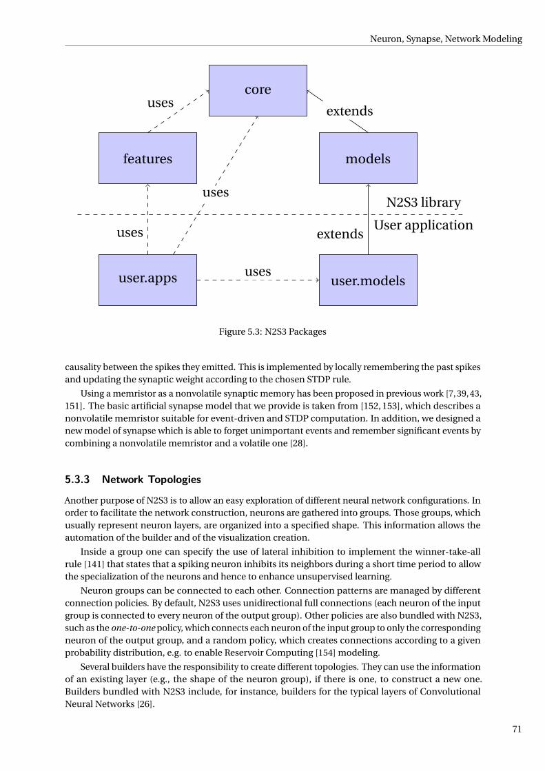
Neuron, Synapse, Network Modeling
core
features models
N2S3 library
User application
user.apps user.models
usesextends
uses
uses
uses
extends
Figure 5.3: N2S3 Packages
causality between the spikes they emitted. This is implemented by locally remembering the past spikesand updating the synaptic weight according to the chosen STDP rule.
Using a memristor as a nonvolatile synaptic memory has been proposed in previous work [7, 39, 43,151]. The basic artificial synapse model that we provide is taken from [152, 153], which describes anonvolatile memristor suitable for event-driven and STDP computation. In addition, we designed anew model of synapse which is able to forget unimportant events and remember significant events bycombining a nonvolatile memristor and a volatile one [28].
5.3.3 Network Topologies
Another purpose of N2S3 is to allow an easy exploration of different neural network configurations. Inorder to facilitate the network construction, neurons are gathered into groups. Those groups, whichusually represent neuron layers, are organized into a specified shape. This information allows theautomation of the builder and of the visualization creation.
Inside a group one can specify the use of lateral inhibition to implement the winner-take-allrule [141] that states that a spiking neuron inhibits its neighbors during a short time period to allowthe specialization of the neurons and hence to enhance unsupervised learning.
Neuron groups can be connected to each other. Connection patterns are managed by differentconnection policies. By default, N2S3 uses unidirectional full connections (each neuron of the inputgroup is connected to every neuron of the output group). Other policies are also bundled with N2S3,such as the one-to-one policy, which connects each neuron of the input group to only the correspondingneuron of the output group, and a random policy, which creates connections according to a givenprobability distribution, e.g. to enable Reservoir Computing [154] modeling.
Several builders have the responsibility to create different topologies. They can use the informationof an existing layer (e.g., the shape of the neuron group), if there is one, to construct a new one.Builders bundled with N2S3 include, for instance, builders for the typical layers of ConvolutionalNeural Networks [26].
71

CH5. N2S3, AN OPEN-SOURCE SCALABLE SPIKING NEUROMORPHIC HARDWARE SIMULATOR
5.4 N2S3 Features
5.4.1 Input Processing
The simulator uses a piped stream system to provide stimuli to the network entities. The input processtypically starts by an input reader, which reads data from files or any external source, followed by anumber of streams that filter the input data before feeding it to the network.
Input readers provided with N2S3 allow to read data in a variety of format, including standardformats such as Address Event Representation (AER), a data format used by spike-based cameras, orMNIST, used in a standard dataset for handwritten digit recognition (see Section 5.4.5 for details aboutthe data).
Subsequent filter streams available in N2S3 include coding streams, which convert raw numericaldata into sequences of spike timings, spike presentation streams (e.g., repeating input spike over agiven period, or shuffling spikes), and modifier streams, that alter the input spikes (e.g., by addingnoise). Users are free to use one or multiple input readers and to combine any number of filter streamsin any order; they may also easily create their own readers and filters.
5.4.2 Visualization tools
Users may observe simulation outputs (spikes, weight values. . . ) through network observers. Networkobservers follow the observer pattern by subscribing to events in the simulation (e.g., when a spikehappens), perform some calculations on such events, and make them visible to the user. Examplesof such observers range from textual loggers to dynamic visualizations of the spikes of each neuron.Concretely, N2S3 provides a spike activity map of the network, a synaptic weight evolution visualizer,and the calculation of evaluation metrics (e.g. recognition rates, confusion matrices. . . ).
5.4.3 Experiment Specification Language
N2S3 includes a dedicated internal Domain Specific Language (DSL) that aims to simplify the creationof simulations. At a higher level of abstraction, users can design experiments (network topology,neuron and synapse properties, observation units. . . ) without having to deal with core features such assynchronization or actor policies. The snippet of code below illustrates (1) the creation of a layer with18 standard LIF neurons with a 20 mV threshold, (2) its full connection to an existing layer (namedoutputLayer), and the addition of two observers: (3) a standard weight observer and (4) a custom(i.e., defined by the user) spike observer. The DSL also allows the definition of different stages for thesimulation (e.g., splitting the simulation into a training phase and a test phase).
val hiddenLayer =n2s3.createNeuronGroup() // (1)
.setNumberOfNeurons(18)
.setDefaultNeuronConstructor( () => new QBGNeuron()
.setProperty(NeuronThreshold, 20 millivolts))
hiddenLayer.connectTo(outputLayer) // (2)n2s3.createSynapseWeightGraphOn(hiddenLayer, outputLayer) // (3)n2s3.addNetworkObserver(new SpikeLogger) // (4)
At a lower level, the DSL can specify how neurons are organized within actors (e.g., deploying allneurons within the same actor or each neuron in a specific actor). Users may use pre-existing policiesor define their own.
72
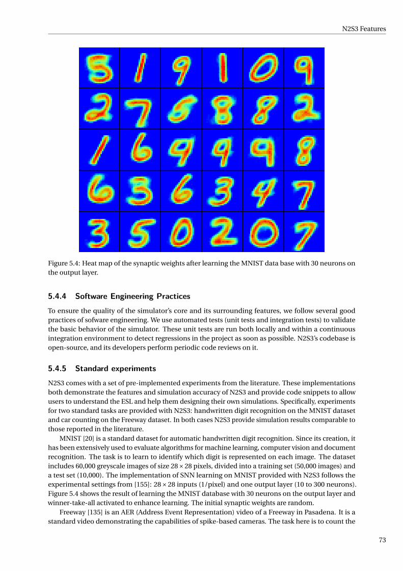
N2S3 Features
Figure 5.4: Heat map of the synaptic weights after learning the MNIST data base with 30 neurons onthe output layer.
5.4.4 Software Engineering Practices
To ensure the quality of the simulator’s core and its surrounding features, we follow several goodpractices of sofware engineering. We use automated tests (unit tests and integration tests) to validatethe basic behavior of the simulator. These unit tests are run both locally and within a continuousintegration environment to detect regressions in the project as soon as possible. N2S3’s codebase isopen-source, and its developers perform periodic code reviews on it.
5.4.5 Standard experiments
N2S3 comes with a set of pre-implemented experiments from the literature. These implementationsboth demonstrate the features and simulation accuracy of N2S3 and provide code snippets to allowusers to understand the ESL and help them designing their own simulations. Specifically, experimentsfor two standard tasks are provided with N2S3: handwritten digit recognition on the MNIST datasetand car counting on the Freeway dataset. In both cases N2S3 provide simulation results comparable tothose reported in the literature.
MNIST [20] is a standard dataset for automatic handwritten digit recognition. Since its creation, ithas been extensively used to evaluate algorithms for machine learning, computer vision and documentrecognition. The task is to learn to identify which digit is represented on each image. The datasetincludes 60,000 greyscale images of size 28×28 pixels, divided into a training set (50,000 images) anda test set (10,000). The implementation of SNN learning on MNIST provided with N2S3 follows theexperimental settings from [155]: 28×28 inputs (1/pixel) and one output layer (10 to 300 neurons).Figure 5.4 shows the result of learning the MNIST database with 30 neurons on the output layer andwinner-take-all activated to enhance learning. The initial synaptic weights are random.
Freeway [135] is an AER (Address Event Representation) video of a Freeway in Pasadena. It is astandard video demonstrating the capabilities of spike-based cameras. The task here is to count the
73

CH5. N2S3, AN OPEN-SOURCE SCALABLE SPIKING NEUROMORPHIC HARDWARE SIMULATOR
Figure 5.5: Input data for the freeway experiment comming from a spike-based camera. The spikesrepresent a variation of intensity for a given pixel and are generated asynchronously.
Figure 5.6: Heatmap showing the reconstruction of the contribution of each input pixel to the activityof the 10 output neurons for the freeway experiment. One can see that some neurons have clearlyspecialized to detect vehicles on a particular lane.
74

Conclusion
number of vehicles passing over each of the six lanes of the freeway. The input data is the spikesrecorded by a spiking camera of resolution 28×28 pixels over a sequence of 78.5 seconds (5.2 millionsspikes). The implementation of the Freeway experiment provided with N2S3 reproduces the experi-mental architecture and settings described in [27]: 2×28×28 inputs, one hidden layer (60 neurones),one output layer (10 neurons), with lateral inhibition on every layer. Figure 5.5 represents the input ofthe neural network and figure 5.6 shows the result of the unsupervised learning process.
5.5 ConclusionWe have presented in this chapter a spiking neural network simulator, N2S3. This simulator is dedi-cated to nanoelectronics-based hardware neural networks. Its simulation strategy is event-based, forprecision and flexibility sakes. As one of the main goals of N2S3 is to promote open research data, i.e.the open distribution of models and experiments for research result reproducibility, it is distributedas open-source software (at https://sourcesup.renater.fr/wiki/n2s3), and a lot of effort hasbeen put in the software architecture, maintainability and enabling features (I/O, graphical outputs,logging, domain specific language). N2S3 is distributed with a few neuron and synapse models. It cansimulate not only feed-forward networks but also convolutional or even recurrent networks. Finally, itis extensively extensible.
We are planning to periodically release new versions in a timeboxed fashion and to perform morequality measurements in the near future, for example: continuous benchmarking and performancetesting to detect non-functional regressions, adding automated code quality and architectural rulesenforcement to detect potential bugs, ensuring the respect for architectural and programming idioms,and agilizing the code reviews.
On the functional side, future work include new models of neurons and synapses, new learningalgorithms and procedures, noise modeling, energy modeling, automatic design space exploration,and new applications.
75


Chapter 6
Combining a Volatile and NonvolatileMemristor in Artificial Synapse toImprove Learning in Spiking Neural
Networks
Abstract
With the end of Moore’s law in sight, we need new computing architectures to satisfy theincreasing demands of big data processing. Neuromorphic architectures are good candidatesto low energy computing for recognition and classification tasks. We propose an event-basedspiking neural network architecture based on artificial synapses. We introduce a novel synapsebox that is able to forget and remember by inspiration from biological synapses. Two differentvolatile and nonvolatile memristor devices are combined in the synapse box. To evaluate theeffectiveness of our proposal, we use system-level simulation in our Neural Network ScalableSpiking Simulator (N2S3) using the MNIST handwritten digit recognition dataset. The first resultsshow better performance of our novel synapse than the traditional nonvolatile artificial synapses.
6.1 IntroductionNeuromorphic computing has the potential to bring very low power computation to future computerarchitectures and embedded systems [18]. Indeed parallel neuromorphic computing, by doing compu-tation and storage in the same devices can overcome the Von-Neumann bottelneck. Neuromorphiccomputing is introduced as an appropriate platform for Big Data analysis and Cloud Computing.Furthermore, many huge projects are running based-on neuromorphic system such as the EU HumanBrain Project [143], the DARPA/IBM SYNAPSE project [144] and deep learning research by Google andFacebook among others.
Recently, emerging devices in nano-scale have demonstrated novel properties for making newmemories and unconventional processing units. One of those is the memristor that was hypotheticallypresented by Leon Chua in 1971 [6] and after a few decades, HP was the first to announce the suc-cessful memristor fabrication [2]. The unique properties in memristor nano-devices such as, extremescalability, flexibility because of analog behavior, and ability to remember the last state make thememristor a very promising candidate to apply it as a synapse in Spiking Neural Network (SNN) [7].
In the recent years, there have been several research works using non-volatile resistive nanodeviceas a synapse to build a SNN hardware [7, 18, 156]. Forgetting in the biological brain is an important keyof adaptive computation, as without forgetting the biological memory soon becomes overwhelmed bythe details of every piece of information ever experienced. Consequently, some studies have been doneusing volatile memory as a synapse in brain-like computing [39, 157, 158]. In this work, we combine
77

CH6. COMBINING A VOLATILE AND NONVOLATILE MEMRISTOR IN ARTIFICIAL SYNAPSE TO IMPROVE LEARNING IN
SPIKING NEURAL NETWORKS
both volatile and non-volatile types of artificial synapses. It leads to make a synapse which can forgetif the information is not important as well as remember if it is significant data.
Thanks to close collaboration with the nano-electronics research center in the University of Lille(IEMN), we have the opportunity of studying the suitability of different kinds of memristors (TiO2,NOMFET, magnetoresistive, magnetoelectric) to build a spiking neural network hardware platform.Due to the demonstrated potential of NOMFET (Nanoparticle Organic Memory Field-Effect Transis-tor) [39, 157] to play the role of a synapse, we use it as a volatile synapse in neuromorphic accelerator.The non-volatile device could be any solid-state memristor. We have chose here the resistive memorypresented in [152] as non-volatile memory.
We evaluate the synapse box proposal by comparing it with a single non-volatile memory synapseby simulation on the MNIST handwritten digit recognition benchmark. We use Leaky Integrate andFire (LIF) neurons in Restricted Boltzmann Machine (RBM) network topology. To run the simulations,we introduce the Neural Network Scalable Spiking Simulator (N2S3), a simulation framework forarchitecture exploration of neuromorphic circuits.
In the next section we describe the architecture including the neuron and synapse models, as wellas the network topology and the unsupervised training algorithm. Then, in Section 6.3 we present theexperimental evaluation of the two different synapses using the MNIST handwritten digit dataset andthe new spiking neural network simulator we propose, N2S3.
6.2 Circuit Design of Neuron and Synapse in RBM Network
In the biological brain, neurons are computing units. Here we define our computing unit by inspirationfrom a biological neuron model. The synapse operates as a plastic controller between two neurons.The manufacturability is out of scope of this research, however in the synapse box, we have applied thereal parameters of volatile synapse beside the model of nonvolatile Resistive RAM. As there are varietiesof nonvolatile memristor fabrications, finding appropriate one that is compatible with NOMFET seemsnot too complicated. It worth mentioning that most of the nanodevices have been reported as ResistiveRAMs (nonvolatile) as well as NOMFET (volatile) are compatible with CMOS circuits [157].
6.2.1 Leaky Integrate-and-Fire neurons
The Leaky-Integrate-and-Fire (LIF) neuron model is a well-studied model of neuron. We discussed itin this dissertation in 4.3.1. We have applied this model of LIF neurons in our work. If there is enoughspikes in the short period of time which depend on the resistor and capacitor value, the neuron reachesto the threshold. Vice versa, if there is no or small number of spikes connected to input of neuron theaction potential decrease and neuron is in leaky phase.
6.2.2 New artificial synapse using memristors
Here, we define our computing unit by inspiring from biological neuron model. The synapse operatesas a plastic controller between two neurons. This plasticity is believed as origin of learning andmemory in brain. Figure 6.1 shows a simple circuit of two neurons connected with an adaptive synapse(memristor).
Before the discovery of a memristor nanodevice, by using state-of-the-art technology, 12 transistorswere combined to mimic the behavior of memristor to perform the STDP learning method [159].Therefore, using a two-terminal and scalable device such as the memristor could save remarkableamount of power and cost specially in modeling large scale Spiking Neural Networks. To modelbiological synapses, not only do we need a device to be able to store the last activity, but it mustalso have enough flexibility to achieve Spike Timing-Dependent Plasticity (STDP) for learning. Usingmemristor as a nonvolatile synaptic memory has been proposed in several works [7, 39, 43, 151]. Byusing nonvolatile memory, we can guarantee to store the last synaptic weight which is necessary for
78

Circuit Design of Neuron and Synapse in RBM Network
a:
b:
pre-synaptic Neuron Post-synaptic Neuron
Synapse
c R cR
Figure 6.1: a) Schematic of two simple biological neurons connected with synapse, b) Leaky Integrated& Fire model of neuron connected with artificial synapse (memristor)
network training but the synapse can not forget. To be able to have a synapse which is able to forget,scientists used a volatile memory cell [157, 158].
6.2.3 New plasticity learning method
Forgetting is a memory mechanism that helps brain having better functionality. In fact, it is believedthat forgetting helps the brain to remember. However, remembering details of many daily activitiesand information such as shopping list, novel book details or newspapers not only are unnecessary toremember but also might interfere with brain functionality for innovative thinking and data analysis.Basically human brain skips details of insignificant information and remembers the most important,unique and surprising events and information. In neuroscience, memorization is believed to achieveas a result of two types of synaptic plasticity: Short-Term Potentiation (STP) and Long-Term Potentia-tion [150]. STP is achieved through the temporal changing of a synaptic connection and the decrease toits initial state soon after. In LTP, stimulation iteration causes permanent synaptic weight achievementas it is depicted in Figure 6.2. Shorter iteration interval leads to more efficient LTP. By inspiring ofthis biological theory, we propose a new artificial synapse with the ability to forget insignificant datawhile storing significant information. The novel synaptic box includes one organic transistor and oneresistive RAM.
STM LTM
Frequent input
Less-Frequent input
Forgetting
Repeat
Input sensory spike
Time
LTP
STP
Conduct
ance
Le
vel
Figure 6.2: Memorization inspired from biology, the data is stored in Long-Term Memory (LTM) ifthe spikes are repeated in a certain time-window, otherwise Short-Term Memory (STM) will storetemporary data.
79

CH6. COMBINING A VOLATILE AND NONVOLATILE MEMRISTOR IN ARTIFICIAL SYNAPSE TO IMPROVE LEARNING IN
SPIKING NEURAL NETWORKS
6.2.4 Combining a volatile and nonvolatile memristor to make a new artificialsynapse
Resistive RAM is modeled in our previous work [13] and is used here as a nonvolatile memristor inthe synapse box. As it is shown in Figure 6.3.b by changing the doped-undoped regions of device, theconductance will be changed. Bigger doped region leads to more conductivity. Therefore by controllingthis boundary between two regions, the conductivity is controlled. The behavior of memristor can bemodeled as follows [2]:
v(t ) = Rmi (t ) (6.1)
Rm = RONw(t )
D+ROF F
(1− w(t )
D
)(6.2)
where Rm is the variable resistance of memristor, w(t ) is the width of the doped region, D is the overallthickness of device, RON and ROF F are device resistances while the active region is completely doped(w = D) and mostly undopped (w → 0) respectively (Figure 6.3.b). To model the changing of theconductance, we use the model extracted from Equation 6.2 and introduced in [153] by consideringgmax = 1
RONand gmi n = 1
ROF Fas the maximum and minimum device conductance respectively.
Organic synaptic memory is a novel memristive device with capability of mimicking synapticproperties especially forgetting ability that we discussed it in Section 2. Here, we use a Nano-particleOrganic Memory Field Effect Transistor (NOMFET) as an organic memristive device made of con-jugated molecules and metal nanoparticles (NPs) which is fabricated by the Institute of Electronics,Microelectronics and Nanotechnology (IEMN) at Lille university [39]. We use NOMFET as our volatiledevice in the synapse box. In the most recent fabrication process [158], NOMFET works at 1 V with atypical response time in the range 100–200 ms. NOMFET is designed particularly for neuro-inspiredcomputing architectures [157]. NOMFET uses charge trapping/detrapping in an array of gold nanopar-ticles (NPs) with the SiO2/pentacene interface designed to mimic dynamic plasticity of a biologicalsynapse as depicted in Figure 6.3 [157]. The NOMFET is used as a two-terminal device by connectingdrain (D) and gate (G) together and using this terminal as an input. The source (S) is used as output ofthe device. Equation 5 shows the behavior of NOMFET as a memristor:
id s(t ) = g (qnp (t ), vd s(t ), t )vd s (6.3)
where g is the conductance of the device, vd s(t ) is the applied voltage and qnp is the charges trappedin the NP. For more details of physical structure and behavior of NOMFET refer to [157, 158].
Figure 6.3.c is the synapse box schematic that we apply in our simulation platform to take theadvantages of both nonvolatile and volatile artificial synapses. The equivalent circuit of transistoris depicted in Figure 6.3.d. Actually, weight modification follows the STP rule until reaching the LTPthreshold in NOMFET. The modification of nonvolatile device is based on STDP learning. Indeedthe NOMFET reacts similar to a high-pass filter (HPF). The stimuli spikes with low frequency are notqualified to pass in forgetting Phase. In LTP, stimuli spikes which have more frequency pass to interferein learning phase (Figure 6.2).
6.2.5 Network topology and learningBy using unsupervised learning inspired by biological neural networks, we propose a fully connectednetwork architecture similar to Restricted Boltzmann Machine [160]. To figure out the correlationbetween the data, STDP helps to adjust the weight if the sensory input spikes are frequent enough topass the STP and remain in LTP phase. In STDP, if there is output spike in pre-synaptic neuron andshortly after in post-synaptic neuron, the conductance of the synapse between two neurons increases.On the other hand, if the post-synaptic neuron spikes shortly before the pre-synaptic neuron, theconductance of synapse between two neurons decreases. For more comprehensive explanation forSTDP, we refer you to Chapter 4. To see how plasticity in memristor helps targeting STDP achievementwe refer you to [161].
80

Experimental Validation
ID
VG
Spikes
PentaceneAu Nanoparticles
p+ silicon
D S
G
Pt PtUndoped Doped
D
W(t)
a:
b:
Drain Source
c+-
m
inout
αVds
c:
d:
G
Figure 6.3: Artificial synapse: a) Schematic view of the NOMFET as a volatile memory, b) TiO2 basednonvolatile memory, c) Synapse box schematic, d) Equivalent circuit with simple elements
The simulator architecture in our work is event-driven, there is no clock to synchronize the inputsand outputs. Furthermore, by inspiring of biological behavior of brain computing, we apply lateralinhibition to reduce the activity of the neighbors of winner neurons. This method is known as winner-take-all (WTA) strategy [162]. The neuron which reaches the threshold first sends an inhibitory signalto all other neurons in the same layer to reset their states during inhibition time.
6.3 Experimental ValidationIn order to check the effectiveness of the synapse, we propose a spiking neural network simulator. Ourrequirements for the simulator are: speed (thus event-driven simulation and concurrency), scalability(thus high-level abstraction and distributability), and adaptability (possibility to model differentsynapses, soma, and network topology). After the presentation of the simulator, we describe ourexperimental setting and discuss the simulation results that show an improvement in recognition ratefor the synapse box with respect to the simple nonvolatile synapse.
6.3.1 MNIST recognition improvement
We have used the MNIST training dataset of handwritten digits [163] to train and test the performanceof neural networks based on the synapse box. The training set consists of 60000 digits between 0 and 9and each handwritten number is a 28 × 28 pixel image. In this simulation, we present the full dataset(60000 images) and full images. Each pixel is connected to one input buffer neuron. Pixel intensityis between 0 to 255 and is transfered to 0 to 22 Hertz spiking frequency using a Poisson distributionduring a 350 ms presentation window. Based on previous similar work [164], we have chosen a delay of150 ms between two images. Therefore, there is sufficient time for membrane potentials of all neuronsto reset back to initial values. The network connection weights are between 0 and 1 initialized using aGaussian distribution.
The hardware platform is a 4 core i7-3687U CPU (2.10GHz × 4). We have simulated differentnetwork topologies consisting of 2 fully interconnected layers, with a fixed input neuron number(28×28 = 784) and different output neuron number. The neuron model is LIF and we evaluate twotypes of synapses: non-volatile (NV) and proposed synapse box (volatile/nonvolatile or VNV).
To measure and evaluate the network classification accuracy after a fully unsupervised learningperiod consisting of the presentation of the full MNIST data set, we label the output neurons using10000 samples of MNIST: After training, we stop all synaptic modification processes such as STDP, STPand LTP. We assign a number class to the output neuron which has most frequent firing rate duringthe presentation of the 10000 labelling samples. Using these labels, we then evaluate the recognitionrate of the network on 10000 different test samples by comparing the known class of the input withthe class of the most firing output neuron. As it was observed in similar works [164] and [152], the
81

CH6. COMBINING A VOLATILE AND NONVOLATILE MEMRISTOR IN ARTIFICIAL SYNAPSE TO IMPROVE LEARNING IN
SPIKING NEURAL NETWORKS
Figure 6.4: Synaptic weights (conductance of non volatile memristor) learned in simulation usingthe synapse box with 100 output neurons. The weights in the corners are random because they werealways filtered out by the volatile memristor and thus are never modified or even read.
recognition rate depends on the number of neurons and synapses, and the number of repetitions ofthe presentation of the dataset to the network. In the experiments, we present 60000 digit the datasetthe smallest number of time that is necessary for learning. That is 1 time for less or equal to 50 outputneurons, 2 times for less or equal to 100 output neurons and 3 times for more output neurons. Withthese numbers of presentations, we obtain recognition rates that are comparable to the state of the art.The running time of the simulations are also comparable to those of similar experiments though it isdifficult to make accurate comparisons.
An example of the conductance weights learned in N2S3 on the MNIST dataset is shown in Figure6.4 for 100 output neurons. As it is obvious in the figure, the border of each digit did not pass theNOMFET high-pass filter because of low frequency changes. This is the impact of forgetting propertiesin synapse box to skip unimportant data or noise. To demonstrate the functionality of the synapsebox, we compare the recognition rate of networks of the same topology but using different synapsemodels: a simple nonvolatile synapse (NV) model and the volatile-nonvolatile (VNV) synapse boxmodel. We have run 10 simulations for each number of output neuron and each synapse. The resultsare summerized in Figure 6.5 showing the distribution of the recognition rates for each configuration.We can conclude that using the synapse box improves the recognition rate in average by a small butconsistent margin.
Although it is not shown in Figure 6.5, we have also made the comparison using 300 output neuronand the best recognition rate we have obtained is 89.4 %.
6.4 Conclusion
In this study, we have introduced a novel synapse box with the possibility to forget and rememberinspired from biological synapse properties. This synapse box is composed of a volatile memristor(NOMFET) followed by a nonvolatile resistive RAM. The volatile memristor acts like a high-pass filterto enhance short term plasticity and the nonvolatile resistive RAM enables long term potentiation.Both work together in the spike timing dependant plasticity unsupervized learning process.
In addition, in this work we have also announced and used our event-based simulator, N2S3(Neural Network Scalable Spiking Simulator). It is specifically designed to simulate hardware spikingneural networks. N2S3 is quite flexible to explore different network architectures, synapse and neuronmodels to help design hardware architectures and VLSI circuits. To evaluate and verify the new synapse
82

Conclusion
Table 6.1: Comparing network architecture efficiency for two synapses: nonvolatile (NV) v.s volatile-nonvolatile (VNV) synapse
#Output #synapses Training NV VNVneurons repetition
20 156802 67,17% 68,73%3 68,35% 70,68%
30 235202 75,05% 77,29%3 76,50% 78,91%
50 392002 77,79% 79,60%3 79,88% 82,12%
100 784002 82,32% 84,83%3 85,11% 86.76%
300 2352002 86,23% 87,59%3 88,23% 89,46%
Figure 6.5: Recognition rate as a function of number of output neurons. In the box plot for eachnumber of neuron, we compare the recognition rate of the two synapse models. The whiskers of thebox plot represent the minimum and maximum recognition rates of the 10 simulations.
83

CH6. COMBINING A VOLATILE AND NONVOLATILE MEMRISTOR IN ARTIFICIAL SYNAPSE TO IMPROVE LEARNING IN
SPIKING NEURAL NETWORKS
box as well as the functionality of the simulator, we have used the MNIST handwritten digit dataset.The first results demonstrate an improvement in recognition rate by using the synapse box over asingle nonvolatile memristor synapse. We will continue to explore the various parameters and devicecombinations to help design the most efficient hardware neural networks as possible.
For future works, we also propose to study different neural network topologies such as deep belief,recurrent and convolutional neural networks to evaluate the synapse box benefits and costs (area,energy, manufacturability, variability) in other contexts.
84

Chapter 7
Evaluation methodology and parameterexploration to improve performance ofmemristor-based spiking neural network
architecture
Abstract
The brain-inspired spiking neural network neuromorphic architecture offers a promising solu-tion for a wide set of cognitive computation tasks at a very low power consumption. Due to thepractical feasibility of hardware implementation, we present a memristor-based model of hardwarespiking neural networks which we simulate with N2S3 (Neural Network Scalable Spiking Simulator),our open source neuromorphic architecture simulator. Although Spiking Neural Networks (SNN)are widely used in the community of computational neuroscience and neuromorphic computation,there is still a need for research on the methods to choose the optimum parameters for better recog-nition efficiency. With the help of our simulator, we analyze and evaluate the impact of differentparameters such as number of neurons, STDP window, neuron threshold, distribution of inputspikes and memristor model parameters on the MNIST hand- written digit recognition problem.We show that a careful choice of a few parameters can significantly improve the recognition rate onthis benchmark.
7.1 IntroductionNeuroinspired computing has the potential to carry very low power computation to future computerarchitectures and embedded systems [18]. Indeed parallel neuromorphic computation, by performingcomputation and storage in the same devices can overcome the Von-Neumann bottleneck. Thereare two broad types of brain-inspired cognitive computations: abstract artificial neural networks(ANNs) and closer to biology spiking neural networks (SNNs) [165]. Machine learning algorithmssuch as classical ANNs and more recently deep belief networks [21, 166] are widely used for dataclassification and clustering. However, ANNs are a highly abstract mathematical model of neuronsthat are designed to be executed on digital traditional von Neumann processing platforms (more andmore using accelerating units such as GPUs). ANNs only use rate coding to represent neuronal activityand are not capable of taking into account the precise relative timing of spikes that are significantwhen dealing with natural signals that are more and more significant in the internet of things. The datashould be coded to spikes to be processed in SNN, which is known as spike coding (versus rate codingin ANN). SNNs offer online real time unsupervised learning through continuous weight updating whichis performed on local synaptic weights. This temporal and spatial locality is important in hardwareimplementations of neural networks because it frees this architecture of the memory bottleneck of Van
85

CH7. EVALUATION METHODOLOGY AND PARAMETER EXPLORATION TO IMPROVE PERFORMANCE OF
MEMRISTOR-BASED SPIKING NEURAL NETWORK ARCHITECTURE
Pre
-synap
tic
Neuro
ns
Post-synaptic Neurons
synapse
a: b:
Figure 7.1: Neuromorphic vs SNN, a) The memristive synapse connects the spiking neurons in config-urable crossbar array suitable for stdp unsupervised learning, the presynaptic neurons are consideredas inputs and postsynaptic neurons play output rolls. b) The spiking neural network two layers of thisthree layers could similarly operates as crossbar array.
Neumann architectures. Recent advances in nanotechnology have provided neuromorphic computingarchitecture with novel memristive devices which have the capability of mimicking synaptic plasticity,such as resistive switching memory (RRAM) [61, 95, 137], phase change memory (PCM) [62, 167, 168],Conductive Bridge memory (CBRAM) [32, 63, 169], and ferroelectric memory (FeRAM) [36, 170]. Theadvantages of using these memristive nanodevices to model the behavior of synapses are their uniqueproperties, such as scalability, flexibility because of their analog behavior, manufacturability on top ofCMOS technology to make a crossbar array (shown in Figure 7.1) and ability to remember the last statein a SNN [7]. Fortunately due to close collaboration with the nano-electronics research center in theUniversity of Lille (IEMN), we have the opportunity to study the appropriateness of various classesof memristors (e.g.,TiO2, NOMFET, Magnetoelectric) to build a SNN hardware platform by using realparameters. The non-volatile resistive switch could be any solid-state RRAM. We have chosen herethe resistive memory presented in [152] as non-volatile memory because it is representative of suchdevices.
It is widely believed that plasticity is the key of learning in the biological brain [171]. Conse-quently, with the latest proposals to use the memristive nano-devices as synapses, we implementan efficient and well-studied unsupervised learning rule known as spike timing dependent plasticity(STDP) [127, 172]. In this study, we show that the memristive synapse is adapted to unsupervised STDPlearning in SNNs. We explain the required technology and architecture with system-level simulation.For implementation and results, we use the MNIST dataset of handwritten digits [163] to test the per-formance of neural networks. Although, there are various research works using STDP learning in SNNarchitecture and neuromorphic VLSI implementations, none of them evaluates and analyzes the keyparameters that improve learning and SNN recognition performance in those architectures. Our maincontribution is to evaluate and explore the impact of several parameters on the learning performanceof SNNs for the MNIST benchmark: the number of neurons in the output layer, the duration of theSTDP window, various thresholds for adaptive threshold LIF neurons, different distributions of spikesto code the input images and the memristive synapse fitting parameter.
86

Experimental evaluation of the influence of four parameters on the classification of handwritten digits
Figure 7.2: Sample heat maps of the synaptic weights after network training with four different numbersof output neurons (20, 30, 50 and 100).
7.2 Experimental evaluation of the influence of four parameters onthe classification of handwritten digits
In this section, we evaluate and explore the effects of four parameters on the performance of thenetwork architecture namely the distribution of input spike trains, the STDP window duration, theneuron thershold, and the synapse β parameter. These parameters will be fully described in thefollowing. The full MNIST dataset is presented twice to the networks with four different numbers ofoutput neurons. A sample of output results is shown in Figure 7.2 for 20, 30, 50 and 100 output neurons.
Simulation has been done using our event-based Neural Network Scalable Spiking Simulator(N2S3). N2S3 has been developed to implement, evaluate and simulate spiking neuromorphic hard-wares. We vary each parameter independently to asses its influence on the recognition rate. Thedefault value for these parameters are taken from the values listed in the literature. We call this set ofparameters the baseline.
Input spike train distribution: Poisson.
STDP window duration: 25 ms.
Neuron threshold: 15 mV.
Synapse β parameter: 1.5.
At the end of this section, in section 7.2.5, we compare the baseline with the best parametersobtained separately and discuss the results.
87

CH7. EVALUATION METHODOLOGY AND PARAMETER EXPLORATION TO IMPROVE PERFORMANCE OF
MEMRISTOR-BASED SPIKING NEURAL NETWORK ARCHITECTURE
Poisson Gaussian Uniform
6800
6900
7000
7100
7200
7300
7400
Neuron=30
Distributions
Rat
e R
ecog
nitio
n X
%
Poisson Gaussian Uniform
6600
6700
6800
6900
7000
7100
Neuron=20
Distributions
Rat
e R
ecog
nitio
n X
%
Poisson Gaussian Uniform
7700
7800
7900
8000
8100
Neurons=50
Distributions
Rat
e R
ecog
nitio
n X
%
Poisson Gaussian Uniform
8300
8350
8400
8450
8500
Neuron=100
Distributions
Rat
e R
ecog
nitio
n X
%
Figure 7.3: The comparison of three different distributions for generating spike train by transfer-ring MNIST database pixels to spike train. These distributions are tested with different number ofneurons=20, 30, 50, 100.
In all the simulations, as the weight initialization is random, each simulation has been repeated 10times and the results are shown in box plots with the default parameters of the box plot function of theR statistical tool.
7.2.1 Effect of spike distribution
As the platform is working using spikes for processing the data, we need to generate spikes train ofthe images of MNIST dataset to extract a spike-based dataset from a frame-based dataset respectingto intensity of each pixel of images. The pixel intensity is between 0 to 255 and should be transfer tothe spike train to be readable by SNN. For instance, Diehl and Cook [164] use a method which themaximum pixel intensity of 255 is divided by 4, resulting in input firing rates between 0 and 63.75Hz. Yet there is a question that with which interval time between two spikes we generate the spikes?Therefore, statistical distribution rules can help to generate appropriate spike train when encode thepixels.
88
Experimental evaluation of the influence of four parameters on the classification of handwritten digits
Poisson input spike train distribution
Here we explain a particular class of random process called a Poisson spike train process. Define ρ(t )response function to the input stimuli:
ρ(t ) =k∑
i=1δ(t − ti ) (7.1)
where k is the total number of spikes in the spike train, and ti defines the time each spikes occurs. Theunit impulse signal is defined as:
δ(t ) =
1 if t = 00 otherwise
(7.2)
The instantaneous firing rate (e.g., of a sensory neuron) can now be formally defined to be the expecta-tion of the sensory input response function which is r (t ) = ⟨
ρ(t )⟩
. The average spike count betweentimes t1 and t2 can then be defined from the instantaneous firing rate:
⟨n⟩ =∫ t2
t1
r (t )d t , (7.3)
the probability of a spike occurring during a given brief time interval is equal to the value of theinstantaneous firing rate during that time interval times the length of the interval:
P(one spike in (t−∆t ,t+∆t )) = r (t )∆t . (7.4)
We assume the instantaneous firing rate r is constant over time. This is called a homogeneousPoisson process. From Equation 7.3 it is derived ⟨n⟩ = r∆t for any interval ∆t = t2 − t1. Equation7.4 can be used to generate a Poisson spike train by first subdividing time into a bunch of shortintervals, each of duration∆t . Then generate a sequence of random numbers x[i ] uniformly distributedbetween 0 and 1. For each interval, if x[i ] ≤ r∆t , we generate a spike otherwise no spike. Thisprocedure is appropriate only when ∆t is small enough for e.g., millisecond range. Using Poissondistribution, we made an event-based version of MNIST [173] and it is available open-source online(https://github.com/MazdakFatahi/evt-MNIST). We refer to intensity of pixels as the probability that aspike occurs within an interval.
Other distributions of the input spike trains
In our simulation, the pixel intensity between 0 and 255 is transferred to 0 to 22 Hz spiking frequencyusing different probability distributions during a 350 ms presentation window. Based on previoussimilar work [164], we have chosen a delay of 150 ms between two images. Therefore, there is enoughtime for membrane potentials of all neurons to reset back to their initial value. The network connectionweights are between 0 and 1 initialized using a Gaussian distribution. We compare uniform, Gaussianand Poisson distribution using different numbers of output neurons in Figure 7.3. This figure showsthat the choice of the input distribution does not have a significant impact on the recognition rate ofthe network. That means that the classification of the inputs is done mainly on the frequency of theinputs regardless of the precise timing of the spikes.
Figure 7.4 depicts recognition rate for different number of neurons using three various spike traindistribution. This figure demonstrate that increasing the number of neuron increase the recognitionrate. We expected such a behavior because increasing the number of neurons will increase the numberof synapse in the network therefore the chance of learning is increased due to more precise coding. Itis worth to note that in general the relation between the number of neuron and learning performanceis not always increasing ratio while we increase the number of neurons. The reason is that the randomselection of number of neurons might cause either overfitting or underfitting problems.
89

CH7. EVALUATION METHODOLOGY AND PARAMETER EXPLORATION TO IMPROVE PERFORMANCE OF
MEMRISTOR-BASED SPIKING NEURAL NETWORK ARCHITECTURE
0 20 40 60 80 10065
70
75
80
Number of output neuron
Rec
ogn
itio
nra
te(%
)
PoissonGaussianUniform
Figure 7.4: The recognition rate of the network using different number of neurons and three spike traindistributions.
7.2.2 Effect of STDP window durationActivity-dependent modification of synaptic weights because of STDP depends on the correlationsbetween pre- and postsynaptic firing over timescales of tens of milliseconds [174]. Contrarily to abiological simulation, as we simulate hardware SNNs, we can choose some parameters. The waySTDP is implemented in hardware is a very important parameter. We use a simplified form of STDP(from [175]) where the weights of the synapses are always slightly decreased except when there is atemporal correlation between a presynaptic firing and a postsynaptic firing during a time window ofduration STDP window. We look here at the influence of this STDP window duration on the learnigcapabilities of our networks.
The duration of the STDP window is related to the frequency of the input spike trains. As themaximum frequency is 63.75 Hz, the STDP window duration should be of approximately the sameduration as the corresponding period, 15.7 ms, or higher. To be able to evaluate the optimum STDPwindow duration, we have started using a 15 ms duration and increasing to 65 ms by increments of10 ms as it is depicted in Figure 7.5.
The results show a low performance using 15 ms regarding to other STDP window durations. Wehave a remarkable improvement from 15 ms to 25 ms and the best results are obtained using the rangebetween 35 ms and 55 ms. At 65 ms, the recognition rate starts to decrease. Our interpretation is that atoo short duration does not allow to capture all the high intensity pixels in the input, and a too longduration is not specific enough as it captures too many mid range pixels and thus is not specific enough.One would need to do additional experiments to check how the STDP window influences the learningspeed of the network. Indeed, here we just check the final network state after two presentations of the60000 images of the MNIST dataset, but the convergence speed of the SNN may well depend also onthe STDP window duration. Figure 7.6 illustrates the average recognition rate of neural networks usingvarious number of neurons.
7.2.3 Effect of neuron thresholdIn our hardware simulation, we use the Leaky-Integrate-and-Fire (LIF) neuron model. This type ofneuron model is fit for SNN architectures [115] due to several properties such as avalablility of low-power CMOS design using subthreshold regime transistor [5], fast to simulate, and particularly efficientfor large-scale network simulations [116].
The LIF model is described in Chapter 4, Equations 4.8 and 4.9. If injected currents from synapsesare large enough, they cause the action potential to pass the threshold voltage, and the neuron fires.It means there are enough input spikes in a short time-window. When there is no or only a smallnumber of spikes in a time-window, the neuron is in the leaky phase and the state variable decreasesexponentially. The duration of this time window depends on τn = RC .
90

Experimental evaluation of the influence of four parameters on the classification of handwritten digits
15 25 35 45 55 65
7400
7600
7800
8000
8200
Neuron=50
STDP Windows
Rat
e R
ecog
nitio
n X
%
83
50
84
00
84
50
85
00
85
50
70
15 25 35 45 55 65
6600
6800
7000
7200
7400
7600
Neuron=30
STDP Windows
Rat
e R
ecog
nitio
n X
%
55 6515 25 35 45
6000
6500
7000
Neuron=20
STDP Windows
Rate
Reco
gniti
on X
%
15 25 35 45 55 65
Neuron=100
STDP Windows
Rate
Reco
gniti
on X
%
Figure 7.5: The comparison of different STDP-window duration for using different number of neu-rons=20, 30, 50, 100. The MNIST digits dataset after converting to the corresponding spikes to thepixels densities, are presenting to the network for 350 ms for (each frame). The 150 ms pause betweeneach digit presenting are considered. This figure illustrates the performance of neural network usingfour various number of neurons and different STDP-windows.
To simulate the LIF neuron, we have to define a threshold for the neuron. Furthermore, we usedthe homeostasis technique to improve the network stability and performance. It means that if one or agroup of neurons are too active when reading the input data, we slightly increase the threshold andvice versa if one or some neurons are inactive during the training process the threshold is decreasedslightly. In this section, we verify and analyze the spiking neural network performance while usingdifferent thresholds for the same neurons to reach the best threshold value. To be able to trace onlythe impact of different thresholds on the system performance, we use the same homeostasis for allneurons with the same rate of increasing and reduction. The range of threshold values have beenchosen to cover the minimum and maximum action potential in the network. Figures 7.7 and 7.8shows the effect of the different thresholds on the recognition rate. The results show that the neuronthresholds between 25 and 35 mV lead to the best recognition rates. However, for the larger numbersof neurons choosing a threshold of 45 mV also leads to an acceptable performance. In contrast, for thenetworks with the smaller numbers of neurons the lower thresholds lead to a good recognition rate inthe network. One could think that it is easily explained because in the networks with more neurons,each neuron is connected to a larger number of other neurons and thus receives more incoming spikesand thus reach its threshold sooner. But here, the number of inputs of the neurons is constant and
91

CH7. EVALUATION METHODOLOGY AND PARAMETER EXPLORATION TO IMPROVE PERFORMANCE OF
MEMRISTOR-BASED SPIKING NEURAL NETWORK ARCHITECTURE
0 20 40 60 80 10055
60
65
70
75
80
Number of output neuron
Rec
ogn
itio
nra
te(%
)
STDP-Window=15 msSTDP-Window=25 msSTDP-Window=35 msSTDP-Window=45 msSTDP-Window=55 msSTDP-Window=65 ms
Figure 7.6: The recognition rate of the network using different number of neuron and six differentSTDP-wnidows.
equal to 28×28 = 784, the number of pixels in the image. Actually, the winner-takes-all rule increasesthe connectivity of the neurons inside the layer, but for inhibitory purposes. In general, the optimalvalue of the neuron threshold depends on the network architecture, and more generally on the activityof the network. In our case, the differences are not large enough to conclude and we would need torun a much larger number of simulations to check if this shift on the optimal value is real or just arandom effect. In Figure 7.8, we compared all four threshold values for having a better comparison.The mean of the ten times running values is considered for this figure. As it is obvious from Figure7.7 small threshold value has better performance with small number of neurons and larger thresholdvalue has better performance with only the larger number of neurons. However if we want to chooseone threshold for neurons in network, definitely the average values (35 and 25 mV) demonstrate betterperformance as it is more obvious in Figure 7.8.
7.2.4 Effect of synapse β parameter
The quality of the synapse and the rate of conductance change of synapses causes influence on thelearning capabilitiesof SNNs. For instance using binary synapses which switch from zero to one willcause much lower performance in learning than using an analog synapse. Therefore the amount ofchange after updating the weights is important. The conductance change does not only depend on theSTDP rule for modification but also on the characteristics of the synapse itself. Here, we evaluate thenetwork learning performance when changing parameters in the synapse to modulate the synapticweight change rate.
For the model of memristor as an artificial synapse, we use the model introduced in [152, 153]which is inspired from experimental memristive devices measurements [41]. The increasing anddecreasing of conductance is presented by Equation 7.5 and Equation 7.6 respectively.
∆gi nc =αi nc e−β g−gmi n
gmax−gmi n (7.5)
∆gdec =αdec e−β gmax−g
gmax−gmi n (7.6)
gmax and gmi n are the maximum and minimum of conductances of the memristor. αi nc and αdec
characterize the conductance step and β is a fitting parameter. To evaluate the impact of synapticconductance on learning in the neural network, we vary the β fitting parameter because it directlyaffects the amplitude of the weight modifications. The other parameters in the simulation are fixedto gmax = 1, gmi n = 0.0001, αi nc = 0.01 and αdec = 0.005. The initial conductance of the nanodevicesbefore starting to train the network are chosen randomly around the mid-range. We observed noremarkable effective impact on the network performance, which is a proof of neural network robustness
92

Experimental evaluation of the influence of four parameters on the classification of handwritten digits
15 25 35 45
6750
6800
6850
6900
6950
7000
7050
Neuron=20
Neuron threshold (mV)
Rat
e R
ecog
nitio
n X
%
15 25 35 45
7100
7200
7300
7400
7500
7600
Neuron=30
Neuron threshold (mV)
Rat
e R
ecog
nitio
n X
%
15 25 35 45
7800
7900
8000
8100
8200
15 25 35 45
Neuron=50
Neuron threshold (mV)
Rat
e R
ecog
nitio
n X
%
8250
8300
8350
8400
8450
8500
Neuron=100
Neuron threshold(mV)
Rat
e R
ecog
nitio
n X
%
Figure 7.7: The comparison of various threshold (15, 25, 35, 45 mV) for using different number ofneurons=20, 30, 50, 100. The threshold between 25 and 35 mV demonstrate better performance in thenetwork, however, in the network with smaller number of neurons the neuron with less threshold havestill acceptable performance and on the contrary in larger neural networks the neuron with more firingthreshold voltage (such as 45 mV using for the 100 output neurons) have demonstrated acceptableperformance too.
0 20 40 60 80 100
70
75
80
Number of output neuron
Rec
ogn
itio
nra
te(%
)
Threshold=15 mVThreshold=25 mVThreshold=35 mVThreshold=45 mV
Figure 7.8: comparing network performance using various number of neuron with different threshold
93

CH7. EVALUATION METHODOLOGY AND PARAMETER EXPLORATION TO IMPROVE PERFORMANCE OF
MEMRISTOR-BASED SPIKING NEURAL NETWORK ARCHITECTURE
1.5 1.8 2 2.5
7000
7100
7200
7300
7400
Neuron=30
Different Beta factors of artificial synapse
Rat
e R
ecog
nitio
n X
%
1.5 1.8 2 2.5
7700
7800
7900
8000
Neuron=50
Different Beta factors of artificial synapse
Rat
e R
ecog
nitio
n X
%
1.5 1.8 2 2.5
8300
8350
8400
8450
8500
8550
Neuron=100
Different Beta factors of artificial synapse
Rat
e R
ecog
nitio
n X
%
1.5 1.8 2 2.5
6200
6400
6600
6800
Neuron=20
Different Beta factors of artificial synapse
Rat
e R
ecog
nitio
n X
%
Figure 7.9: The comparison of various fitting parameters (β) for using different number of neurons=20,30, 50, 100. The results demonstrate better performance using β between 1.8 and 2. However, thedifferences are not distinguishable which is a prove of memristor devices robustness to the variations.
Synapse Distrib. STDP w. Thres. β
Best VNV Poisson 55 ms 35 mV 2Baseline NV Poisson 25 ms 15 mV 1.5
Table 7.1: Best parameters vs. baseline parameters
to variations as is reported in [175]. The results for four different number of neurons in the outputare presented in Figure 7.9 and 7.10. Although the network performance variation using different βparameters is not remarkable, the results demonstrate slightly better performance using β between 1.8and 2.
7.2.5 DiscussionAs a final experiment we compare the baseline (values inspired by the litterature) with the best values forall the evaluated parameters, including the volatile/non volatile synapse of Chapter 6. The parametersare listed in table 7.1. Other network elements and parameters that are not listed in table 7.1 are thesame for both models.
We have evaluated both models using the same number of output neurons that were used inthe parameter evaluation sections with the addition of 300 neurons for the output layer. The resultsin Figure 7.11 demonstrate enhanced performance using the best obtained parameters rather thanbaseline parameters. These results, as most simulations shown in this study, show that the variation of
94
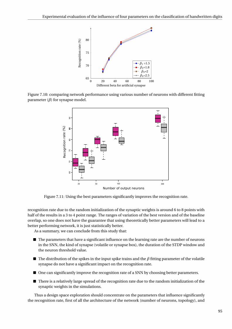
Experimental evaluation of the influence of four parameters on the classification of handwritten digits
0 20 40 60 80 10065
70
75
80
Different beta for artificial synapse
Rec
ogn
itio
nra
te(%
)
β1 =1.5β2=1.8β3=2β4=2.5
Figure 7.10: comparing network performance using various number of neurons with different fittingparameter (β) for synapse model.
50
65
70
75
80
85
85
90
100 30020
Number of output neurons
Reco
gnit
ion r
ate
(%
)
Figure 7.11: Using the best parameters significantly improves the recognition rate.
recognition rate due to the random initialization of the synaptic weights is around 6 to 8 points withhalf of the results in a 3 to 4 point range. The ranges of variation of the best version and of the baselineoverlap, so one does not have the guarantee that using theoretically better parameters will lead to abetter performing network, it is just statistically better.
As a summary, we can conclude from this study that:
The parameters that have a significant influence on the learning rate are the number of neuronsin the SNN, the kind of synapse (volatile or synapse box), the duration of the STDP window andthe neuron threshold value.
The distribution of the spikes in the input spike trains and the β fitting parameter of the volatilesynapse do not have a significant impact on the recognition rate.
One can significantly improve the recognition rate of a SNN by choosing better parameters.
There is a relatively large spread of the recognition rate due to the random initialization of thesynaptic weights in the simulations.
Thus a design space exploration should concentrate on the parameters that influence significantlythe recognition rate, first of all the architecture of the network (number of neurons, topology), and
95

CH7. EVALUATION METHODOLOGY AND PARAMETER EXPLORATION TO IMPROVE PERFORMANCE OF
MEMRISTOR-BASED SPIKING NEURAL NETWORK ARCHITECTURE
then tune the other parameters. This design space exploration should be based on a statistical analysisof the performance of the network by running several simulations for each combination of parametervalues. Finally, researchers should explain clearly what they mean when they give a single number asthe recognition rate of a given SNN, is it a mean of several rates, the best rate or just a single rate.
7.3 ConclusionsWe have presented an empirical study of the influence of several parameters on the recognition rate ofmemristor based hardware SNNs on the MNIST benchmark. This study is based on simulations runwith N2S3, an open source simulator we have developped to help design neuromorphic circuits.
This study has shown that not all parameters have a significant influence on the learning rate ofSNNs and thus that a design space exploration should concentrate first on the architecture of thenetwork; then, the kind of device used as a synapse, the STDP mechanism used and its parameters,and the threshold of the neuron. This study is only valid on the MNIST benchmark and shouldbe complemented by similar studies on other test cases to confirm these findings, especially testcases using natural data in spiking form where the precise relative timings of the input spikes wouldnecessitate more precise STDP mechanisms than the simplified one used in this study that is onlysensitive to the average frequency of the input spike trains.
In the future, we will explore different models of synapses and neurons, more complex networktopologies and STDP mechanisms, and enhance the N2S3 simulator with automatic design spaceexploration facilities that will concentrate on optimizing the most significant parameters discovered inthis study. In addition to the recognition rate (or classification capabilities), we will also evaluate otherperformance measures such as the power consumption of the circuit or its convergence speed.
96

Chapter 8
Deep learning in spiking neural network
Abstract
Deep learning recently is used in several state-of-the-art studies and developments due to itsability in pattern recognition data classification. Most of the research work and applications arein machine learning domain. In this chapter, we introduce a framework to use the proposed ratebased version of Contrastive Divergence (CD) updating weight rule. Respecting to the rate aspectof neural coding, we develop a Spike-Based Deep Belief Network (S-DBN) with Leaky Integrate-and-Fire (LIF) neurons and the model is evaluated using ORL face detection dataset. The proposedmethod provides a suitable framework that can be used in implementing deep architectures in theneuromorphic hardware systems.
8.1 IntroductionDeep learning is currently very active research area in machine learning and pattern recognitionsociety due to its potential to classify and predict as a result of processing Big data and Internet ofThings (IoT) related data. The implementation on neuromorphic hardware platforms emulatinglarge-scale networks of spiking neurons may present important advantages from the perspectivesof scalability, power dissipation and real-time interfacing, and better recognition performance inneural network learning [176]. Considering brain mechanisms, prerequisite for an intelligent systemis utilizing multi- level architecture such that each level of the model provides extracted features forthe next one. This approach of feature extraction leads the system to implement complex functionsusing higher level of abstraction. Deep Learning is a set of powerful machine learning methods fortraining deep architectures. Considering the inherent inefficiency of learning methods from traditionalArtificial Neural Networks in deep architectures, Contrastive Divergence (CD) has been proposed totrain Restricted Boltzmann Machines (RBM) as the main building blocks of deep networks [33]. Deeparchitectures can be developed by stacking RBMs and training the layers using Contrastive Divergence(CD) as the most efficient algorithm in deep learning in a greedy layer-wise approach [21].
Despite the proficiency of deep architectures in machine learning tasks, implementing thesemodels in common platforms can be a very time and resource consuming process. The conventionaldigital computers because of using Von Neumann architecture, waste too many energy specificallythrough storing results and retrieving data in/from memory elements [177]. The neuro-inspiredcomputational platform which has memory next to the computation unit, could be an alternativesolution for efficient computation using CD algorithm. Spiking Neural Networks (SNN) are more closeto biological neurons rather than abstract mathematical models. The important aspect of spikingmodel of neurons is its potential for hardware implementation as a very specific and power efficienthardware accelerator. In SNN the neurons communicate using spikes [34]. Therefore, we have todesign an NN architecture that implement spiking data. In this chapter, we present a framework forusing Contrastive Divergence to train an SNN using RBM and spiking LIF neurons. This framework
97

CH8. DEEP LEARNING IN SPIKING NEURAL NETWORK
Boltzmann Machine Restricted Boltzmann Machine
Figure 8.1: Restricted Boltzmann Machine is a network of neurons which neurons in one layer areconnected to all neurons in the next layer.
can open a new window toward the neruromorphic architecture designer to apply the state-of-the-artof machine learning learning algorithm in SNN architecture.
To overcome the challenge of using spiking neurons in machine learning domain, one uses theabstract model of neuron. OConnor et al. [94] applied an abstract model of Leaky Integrate-and-Fire (LIF) neuron called Siegert neuron [178] to approximate the average of output firing rates ofLIF neurons. Using this abstract model as a unit of a Deep Belief Network (DBN) and exploitingthe standard Conterastive Divergence (CD) algorithm, they have trained an DBN and the adjustedweights are transferred to a functionally equivalent Spiking platform of LIF neurons. Using such anoffline learning approach, all the weights are fixed and no weight adjustments can be performed inapplication platform.
Spike-Timing Dependent Plasticity (STDP) as the main Hebbian-based learning method, is usedfor updating the synaptic weights in SNN [34]. This spike-based learning rule in a time-averaged can beinterpreted as anti-Hebbian and Hebbian correlations between input and output spikes [179]. In [176]utilizing an abstract model based on neural sampling a STDP-based version of CD has been proposedand a single RBM is trained online successfully.
In this work, regrading the rate aspect of neural coding, we proposed a rate coded contrastivedivergence as an online learning rule for spike-based RBM. Consequently, using the proposed learningapproach, an acceptable accuracy of a Spike Based DBN is demonstrated.
Finally, the remainder of this study is organized as follows. In Section 8.2, we discuss the math-ematical backgrounds of the CD and compare the spike coding with the rate coding in the neuralarchitecture. In Section 8.3, after studying the preliminary principles of an online model, a contrastivedivergence adapted to the spike-based RBMs is proposed. The proposed approach is developed andverified in Section 8.4 for a single spiking RBM and also for the desired Spike-Based Deep Belief Net-work. The model is evaluated in Section 8.5. Finally, the conclusion as well as future possible workshave been discussed in Section 8.6.
8.2 Restricted Boltzmann Machine and Contrastive Divergence
Restricted Boltzmann machines, as a model of artificial neural networks, have been driven fromBoltzmann machines. RBM consists of binary stochastic units connected to each other using bidirec-tional edges. It can represent a probabilistic distribution to learn the basic features of an unknowndistribution using observed data, which is considered as the training data. Generally, training inBoltzmann machine, as fully Recurrent Neural Network (RNN), is involved with a large number ofcomplex computations. Therefore, applying some restrictions to the Boltzmann machine topologyleads to a less complex structure called Restricted Boltzmann Machine (Figure 8.1). From a structuralpoint of view, RBM has one visible and one hidden layer, where all the units in the visible and hiddenlayers are symmetrically connected, but there is no visible-visible or hidden-hidden connection. Thestructure of the Boltzmann machine is related to the proposed structure in 1982 by John Hopfield [108].The Hopfield model is driven from thermodynamic systems and can be quantified through equilibriumenergy. Each state of the Boltzmann machine can be expressed as a value called energy of the state.
98

Deep learning in artificial neural networks versus spiking neural networks
Equation 8.1 presents the energy function of a given RBM as a restricted type of Boltzmann machine.
E(V , H) =−∑i
∑j
vi h j wi j −∑
iai vi −
∑j
b j h j , (8.1)
where E is the total energy of the network, vi is the state of visible i th unit, h j is the state of j th hiddenunit, wi j is the weight between vi and h j , ai and b j are the biases. The assigned probability to eachconfiguration of the network states are:
p(V , H) = 1
Ze−E(V ,H), (8.2)
where Z =∑V H eE(V ,H) is a partition function. RBM, as a generative model, tries to generate an internal
representation of its environment. Increasing the log-probability of the generating input data vectorusing equation 8.2 leads to contrastive divergence [180] updating weight rules for RBM:
∆wi j = η(< vi h j >d at a −< vi h j >model ). (8.3)
In equation 8.3, < vi h j >d at a represent the expectation under the distribution specified by input datavector and < vi h j >model is the expectation under the distribution specified by internal representationof the RBM model. Also the probability of h j using a given V as the input data vector, for each j inhidden layer is 1 with probability p(h j = 1|V ):
p(h j = 1|V ) =σ(b j +Σi vi wi j ), (8.4)
when σ(x) is the logistic sigmoid function and can be defined as:
σ(x) = 1
1+ex (8.5)
In contrastive divergence using Gibbs updating chain (initiated with training data) and iterationsampling for a limited time, the approximated value for < vi h j >model can be computed perfectly[180, 181]. A single step of Gibbs sampling using H as a given hidden vector can be expressed as
p(vi = 1|H) =σ(ai +Σ j h j wi j ). (8.6)
According to [181] only one step of contrastive divergence (C D1), can provide an acceptable approx-imation of gradient of the log probability of the training data and iterating the process for k timesprovides a more precise value:
(∆wi j )k = η(< vi h j >0 −< vi h j >k ), (8.7)
when < vi h j >0 is equal to < vi h j >d at a and < vi h j >k means iterating Gibbs sampling for k times.Also the biased will be updated using these equations:
(∆ai )k = η(vi0 − vi
k ), (8.8)
and(∆b j )k = η(h j
0 −h jk ). (8.9)
8.3 Deep learning in artificial neural networks versus spiking neuralnetworks
Artificial Neural Networks as a tool of artificial intelligence can demonstrate high level of accuracyin machine learning problems and specifically in face recognition applications [182, 183]. On theother side the brain inspired models and specifically Spiking Neural Networks are very suitable to
99

CH8. DEEP LEARNING IN SPIKING NEURAL NETWORK
Figure 8.2: Siegert abstract neuron model [184]
be implemented in VLSI. Therefore, to have a biological model of neural networks in hardware levelSNN is applied. The SNN can be trained using an unsupervised Hebbian-based learning rules such asSpike-Timing Dependent Plasticity (STDP). However respecting to the deep architecture of the brainto have a deep SNN, we have to use efficient algorithms for deep architectures.
Spiking model of neuron uses short pulses (spikes) to coding data [34]. Since the shape of spikesare generally the same, then the rate and the time of spikes are the determinant parameters in datatransferring in biological models. Comparing the biological inspired model to machine learningalgorithms, it is obvious that the time parameter has no role in data coding in machine learningdomain. Consequently, we have to overcome this gap between ANN and SNN if we want to usemachine learning algorithms (e.g., ANN) in SNN platforms.
In this study, we use the Siegert neuron model that can approximate the mean firing rate of LeakyIntegrate-and-Fire neurons with Poisson-process inputs. Siegert abstract model using mathematicalequations can estimate the input-output rate transfer function of Leaky Integrate-and-Fire neurons.Figure 8.2 shows the equation of the Siegert neuron [178, 184]. SNNs use spike trains with randomlydistribution of spike times. To be able to use Siegert model as a unit in our network, we assume thespike trains are Poisson-process with specific firing rates (λi n). As it is depicted in Figure 8.2, the Siegertmodel receives excitatory and inhibitory inputs where λe is the excitatory and λi is the inhibitory ratesof incoming spike trains from pre-synaptic neurons. we and wi are the corresponding synaptic weights.Due to more simplicity, we did not categorize the neurons to excitatory and inhibitory neurons. Weassume λi n as total input spike rates from pre-synaptic neurons as well as w which indicate the both ofwe and wi . By normalizing the values of pixels of an image, we can convert the density of each pixel tothe spike rate of corresponding pixel such that brighter pixel has higher spike rate and darker one hasless firing rate. LIF neuron parameters can be set by adjusting the corresponding variables in Siegertequation. Table 8.1 shows the given values for the membrane time constant (τm), the resting potential(Vr est ), the reset potential (Vr eset ), the threshold potential (Vth) and the absolute refractory time (tr e f ).
In the following sections stacking the proposed RBM with Siegert units, we developed a Deep BeliefNetwork. In this network, after training phase, we transferred the weight matrix to a DBN with LIF unitsusing Brian simulator [146] to evaluate the proposed model. According to the equality between Siegerttransfer function and LIF transfer function, we can use the LIF neurons with the same parameters(Table 8.1).
100

Developing and Training Deep Belief Network with Siegert Units
Table 8.1: LIF parameters
Parameter Description value
τm Membrane time constant 5secVr est Resting potential 0Vr eset Reset potential 0
Vth Threshold potential 5mvtr e f Absolute refractory time 2ms
Figure 8.3: Stacking RBMs as the main building blocks of DBN
Figure 8.4: Some sample images from ORL dataset
8.4 Developing and Training Deep Belief Network with SiegertUnits
The RBMs with Siegert units can be trained in machine learning domain. In fact in this model themean firing rate of input spike trains will be used instead of spike trains.
Hinton et al. introduced an efficient Deep Belief Networks (DBN) for the first time [21]. Theyhave proposed a greedy layer wised algorithm to train the DBN by training each RBM sequentially.Figure1 8.3 illustrates the stages of stacking RBMs. In this work, we use the Olivetti Research Laboratory(ORL) face detection dataset from Cambridge, UK 2. This dataset originally contains 400 grey scale faceimages of 40 distinct volunteers. Figure 8.4 shows some images of ORL dataset. In this chapter, weuse a resized version of ORL that has been proposed in [185]. The input images with 32×32 pixels areused as input vectors with 1024 elements. According to [186], in each step of RBM training process,a
1http://deeplearning.net/tutorial/2The source of the Database of Faces: http://www.cl.cam.ac.uk/research/dtg/attarchive/facedatabase.html
101

CH8. DEEP LEARNING IN SPIKING NEURAL NETWORK
Second RBM
(580*500)
First RBM
(1024*500)
500 hidden units
500 hidden units 80 softmax units
1024 visible units
Figure 8.5: The proposed DBN with Siegert neurons for learning ORL
Figure 8.6: Visualizing the learned features by hidden units
mini-batch of training data consisted of a small subset of all training data is used. The proposed DBNarchitecture, respecting to the size of training vectors, is depicted in Figure 8.5. The first RBM has1024 (32×32) units in visible layer and 500 units in hidden layer. This RBM is trained without any label(unsupervised learning) to provide abstract features for the second one. After training the first RBM,the second RBM is trained using the extracted features generated in previous step. In the recent RBMas a classifier, we use the joint of 500 extracted values and 80 softmax units. The labels of ORL imageshave been converted to softmax vectors. For the first class of images the two first bits are one andothers are zero. For the next one, the two first bits are zero, the next two bits are one, and the others arezero and so on.
We divided the ORL images into two subsets. The first one is the training set and consisted of 8images from 10 of each class. These images are used to train the model and are not used for testing.The second one is the test images containing 2 of 10 from each class. Because of the full connectionsbetween each visible unit and each hidden unit, the dimensions of the arriving connections at eachhidden unit are the same as the dimension of input images. Figure 8.6 shows the correspondingweights of connections between all visible units and 100 randomly selected hidden units. The weightvectors has been reshaped as 32×32 images. During the learning process the hidden units have learnedsome specific features such that they can be triggered only with those specific features. Visualizingthese weight vectors (Figure 8.6), displays the learned features by each hidden unit. Therefore, it is aappropriate monitoring method to study the network learning process [186]. As we can see in Figure8.7, the training process needs too many iterations to reach a proper result. For this model whichis implemented in Matlab, after about 800 iterations, the results are close to 90%. The maximumvalue, 93.2%, corresponds to iteration 1910th . In this study, we use the free energy function (equation8.10) to find the predicted label. Using this function, each possible label has been tested to find theconfiguration with the lowest energy. The corresponding label to the recent configuration is assumedas the predicted label [186].
F (V ) =−∑i
vi ai −∑
jlog(1+ex j ) (8.10)
where x j = b j +∑i vi wi j .
102

Evaluating the model
0 500 1000 1500 20000
10
20
30
40
50
60
70
80
90
100Accuracy evaluation
Number of iterations
Rec
ogni
tion
Acc
urac
y [%
]
Figure 8.7: Accuracy of the proposed DBN with Siegert neurons in face recognition on ORL dataset
0 200 400 600 800 10000
10
20
30
40
50
60
70
80
90
100
Epochs
Rec
ogni
tion
Acc
urac
y [%
]
Accuracy evaluation: Effect of mini−batch size
10204080160
Figure 8.8: Decreasing the number of epochs and increasing the mini-batch size can reduce the modelaccuracy
The accuracy of the model depends on the learning parameters [186, 187]. For example Figure 8.7shows the results when the mini-batch size is 4. The effect of changing the parameters of model usingless iterations and using various mini-batch sizes is depicted in Figure 8.8 . Obviously, less iteration andlarger mini-batch size lead to less accuracy. Eventually, if one is interested in more precise accuracy, itcan be possible through adjusting the learning parameters and also the Siegert neuron parameters(Table 8.1).
8.5 Evaluating the model
Thanks to the equality between the Siegert neuron’s transfer function and the LIF transfer function,without any adjustments, the trained weight matrix in the previous section can be copied to a networkwith the same topology consisted of LIF neurons with the same parameters (Tabel 8.1). To developsuch a network with LIF neurons, we use the Brian simulator. Brian is a simulator for Spiking NeuralNetworks. This simulator is written in the Python programming language. Because of using develop-ment tools such as SciPy module, Python provides very fast routines for mathematical operations andspecifically matrix operations [146]. We have developed a Deep Belief Network in Brian simulator withsame topology as the one that has been implemented in Matlab. In this model since we want to testthe accuracy of the model in a more realistic situation, the equation of LIF neuron (Equation 8.11) isapplied besides the described parameters in Table 8.1.
τmd v
d t=−(v(t )− vr est )+RI (t ) (8.11)
103

CH8. DEEP LEARNING IN SPIKING NEURAL NETWORK
Figure 8.9: The upper row shows 10 of the training images and the lower one illustrate the correspond-ing reconstructed images
Figure 8.10: The upper row shows 10 of the test images and the lower one illustrate the predictedimages
We know the spiking model uses spike trains instead of the real numbers. In Section 8.4, we discussedthe assumption to use the normalized value of the pixels to produce the related firing rate. Conse-quently in this section to test the proposed spiking model, we have to convert the firing rate to the spiketrains. In [173], we have presented more in details the converting approach for MNIST handwrittendigits. In Brian simulator, using PoissonGroup function, we can generate spike trains with specifiedfiring rates. Therefore, the network can be tested with spike trains corresponding to the density ofpixels of the test images. Having the trained weights matrix, despite of the Matlab model, the labelsare not used in the second RBM for training however, they are used as the outputs of the model forclassifying the input images [188]. Respecting to the generative characteristic of DBNs, the model notonly can reconstruct the input images as the internal representations of the given images (Figure 8.9),but also can generate the corresponding learned labels as the predictions of the model. To evaluatethe model in a spiking framework after transferring the weights matrix, the generated spike trainsof test images are passed through the entire of the network. Furthermore, comparing the predictedlabels with the original labels, we compute the model accuracy. Figure 8.10 shows predicted imagesrespecting to the input test images. In addition, as it was predictable, the results of the model with LIFneurons have not changed considerably. However because of the difference between floating numberprecision in Matlab and Brian simulator reloading the weights matrix in Python can cause a smalldecreasing in accuracy. The accuracy of the model in Brian simulator is reduced to 92.4%.
8.6 Conclusion and future works
The ability of brain-like computing has motivated us to evaluate a model with biological structurein face recognition application. Regarding the brain as a deep neural network, we have proposed adeep neural network with spiking neurons to understand if the brain-like models are suitable for facerecognition applications. The proposed model is different from a traditional neural network. Indeedthis model is a Spike-Based deep model with biological inspired neurons (Leaky Integrate-and-Fireneurons). Considering the results of Deep Belief Networks in various tasks in Machine learning domain,a DBN with two RBMs has been developed in Matlab with Siegert units. Consequently, the trainedweights matrix is transferred to a Spiking DBN with LIF neurons. The recent model is simulated in theBrian simulator and the results show the capability of the Spiking Deep Belief Networks in a simpleface recognition application.
For future works, we will take into account using other types of deep models such as Deep Autoen-coders or Convolutional Neural Networks. In this work, we had to train the model in one platform andusing the trained weights in another one. Indeed our model is an offline training model. Using the
104

Conclusion and future works
same platform for training and utilizing the model leads us to an online model of training, which canbe considered as the next work. Additionally, we are looking for a way to perform the same work in asingle platform more suitable for hardware implementation by using the emerging nanodevices suchas memristor to realize the synapse model.
105


Chapter 9
Conclusion
The growing use of ICT devices and technologies in our daily life increases the demand for highperformance, fast (parallel) and power-efficient computations. In present computing architecture, theway of communicating between memory and central processing unit (CPU) is not efficient particularlywhile we are facing the problem of Big Data processing. The reason of this inefficiency is called thememory wall issue or Von Neumann memory bottelneck. This memory bottelneck issue is because ofspeed disparity between the CPU and memory outside the CPU chip.
As we are reaching to the end of Moore’s law, the possibility of increasing the pulse clock of CPUsin order to increase the speed of system is facing serious problems. The multi-core processor was asolution for the power dissipation problem. However, memory hierarchy and memory managementwould be more significant and difficult in multi-core processors. Therefore, the memory wall problemis actually worse in multicores.
New unconventional computing techniques using the emerging nano-devices such as memristorshave been proposed as solutions to Von Neumann architecture problem. Here in this dissertation, westudy the different possibilities of using this nano-device both as a digital logic and analog memristiveswitch. Therefore, we began our research with a feasibility study of using memristive devices indifferent domains. We briefly review the literature about memristors from mathematic model to thephysical realization and its applications. We discuss different classes of memristors based on thematerial used to build the devices. Four general memristive devices are studied in the first chapter:resistive, spintronic, organic (polymeric) and ferroelectric memristors. The potential application aswell as advantages versus disadvantages of using each one are presented too. The resistive memristorhas been used more than others in different research works from memory to artificial synapse. Thespintronic and ferroelectric devices show promising properties to make new nonvolatile memories.The organic memristor is more appropriate to make artificial synapse in Spiking Neural Networks.
In the digital domain, using the capability of memristors to have the processor and the memoryin the same unit, we propose two different architectures using non-volatile memristors. The firstapproach is based on material implication and the second one is based on crossbar arrays. A library oflogic gates are provided using both methods. We compare both methods and the reconfigurability isthe most significant advantage of using the crossbar array architecture.
Neuromorphic computation using Spiking Neural Networks (SNNs) has been proposed as anotheralternative solution for the future of high performance computation. Neurons communicate togetherusing spikes. Therefore different spike codings have been discussed to improve data transferringand data processing in neuro-inspired computation paradigms. Choosing the appropriate neuralnetwork topology could result in better performance of computation, recognition and classification.The model of the neuron is another important factor to design and implement SNN systems. Thespeed of simulation and implementation, the ability of integration to the other elements of network,and the suitability for scalable networks are the factors to select an optimized neuron model. Thesequential order of pre- or postsynaptic spikes occurring across a synapse in an interval of time leads
107

CH9. CONCLUSION
to define different learning methods. In chapter 4, we studied the differences among the methods tohelp to choose the most adapted STDP method to a given network.
We present N2S3 (for Neural Network Scalable Spiking Simulator), an open-source simulator that isbuilt to help design spiking neuromorphic circuits based on nanoelectronics. N2S3 is an event-basedsimulator and its main properties are flexibility, extensibility, and scalability. N2S3 has been developedfrom the ground up to model various kinds of neuron and synapse models, various network topologies,various learning procedures, various reporting facilities, and to be user-friendly, with a domain specificlanguage to easily express and run new experiments. Experimental set up for two standard tasksare provided in N2S3: handwritten digit recognition on the MNIST dataset and car counting on theFreeway dataset.
Furthermore, we have introduced a novel synapse box with the possibility to forget and rememberinspired from biological synapse properties. This synapse box is composed of a volatile memristor(NOMFET) followed by a nonvolatile resistive RAM. The volatile memristor acts like a high-pass filterto enhance short term plasticity and the nonvolatile resistive RAM enables long term potentiation.To evaluate and verify the new synapse box as well as the functionality of the N2S3 simulator, wehave used the MNIST handwritten digit dataset. The first results demonstrate an improvement inrecognition rate by using the synapse box over a single nonvolatile memristor synapse.
We reviewed the most important existing platform in neuromorphic computing domain. Addition-ally We have presented an empirical study of the influence of several parameters on the recognitionrate of memristor based hardware SNNs on the MNIST benchmark. This study has shown that notall parameters have a significant influence on the learning rate of SNNs and thus that a design spaceexploration should concentrate first on the architecture of the network; then, the kind of device usedas a synapse, the STDP mechanism used and its parameters, and the threshold of the neuron. Thisstudy is only valid on the MNIST benchmark and should be complemented by similar studies on othertest cases to confirm these findings, especially test cases using natural data in spiking form where theprecise relative timings of the input spikes would necessitate more precise STDP mechanisms thanthe simplified one used in this study that is only sensitive to the average frequency of the input spiketrains.
Deep learning recently is used in several state-of-the-art studies and developments due to itsability in pattern recognition data classification. Finally, we have proposed a deep neural networkwith spiking neurons to verify the functionality of the brain-like models in SNN for face recognitionapplications. We introduced a framework to use the rate based version of Contrastive Divergence (CD)updating weight rule. Indeed this model is a spike-based deep model with biological inspired leakyintegrate-and-fire neurons. Considering the results of Deep Belief Networks (DBNs) in various tasksin machine learning domain, a DBN with two restricted boltzmann machines has been developed inMatlab with Siegert units. Then the trained weights matrix is transferred to a spiking DBN with LIFneurons. The recent model is simulated in the Brian simulator and the results show the capability of theSpiking Deep Belief Networks in a simple face recognition application is comparable with traditionalmachine learning performance.
To introduce the potential of the future works, there are several possibilities not only in uncon-ventional computing domain but also in using emerging technologies such as memristor. The mixcombination of memristive devices using different materials propose new research studies on thecapability of both devices such as what we have proposed in Chapter 6.
As a proposition for the next study in digital domain, one can organize a Programmable LogicDevice (PLA) platform in such a way that the crossbar array operates as a programmable AND arraybeside material implication as a fixed connection for the OR array. Therefore new generation of FPGAcould be the next target of such a study.
For future work in neuromorphic and SNN field, as they are not well-studied yet, there are plentyof spaces for research in this domain. Studying different neural network topologies such as deepbelief, recurrent and convolutional neural networks to evaluate the different memristive synapsesconsidering the costs (area, energy, manufacturability, variability). We can explore different models ofsynapse and neurons, more complex network topologies and STDP mechanisms, and enhance the
108

N2S3 simulator with automatic design space exploration facilities that will concentrate on optimizingthe most significant parameters discovered in this study. In addition to the recognition rate (orclassification capabilities), we can also evaluate other performance measures such as the powerconsumption of the circuit or its convergence speed.
109


Bibliography
[1] Charith Perera, Arkady Zaslavsky, Peter Christen, and Dimitrios Georgakopoulos. Sensing as aService Model for Smart Cities Supported by Internet of Things. arXiv:1307.8198 [cs], July 2013.arXiv: 1307.8198.
[2] Dmitri B. Strukov, Gregory S. Snider, Duncan R. Stewart, and R. Stanley Williams. The missingmemristor found. Nature, 453(7191):80–83, May 2008.
[3] Massimiliano Di Ventra and Yuriy V. Pershin. Memcomputing: a computing paradigm to storeand process information on the same physical platform. CoRR, abs/1211.4487, 2012.
[4] Giacomo Indiveri and Shih-Chii Liu. Memory and information processing in neuromorphicsystems. Proceedings of the IEEE, 103(8):1379–1397, August 2015. arXiv: 1506.03264.
[5] Giacomo Indiveri, Bernabé Linares-Barranco, Tara Julia Hamilton, André van Schaik, RalphEtienne-Cummings, Tobi Delbruck, Shih-Chii Liu, Piotr Dudek, Philipp Häfliger, Sylvie Renaud,Johannes Schemmel, Gert Cauwenberghs, John Arthur, Kai Hynna, Fopefolu Folowosele, SylvainSaighi, Teresa Serrano-Gotarredona, Jayawan Wijekoon, Yingxue Wang, and Kwabena Boahen.Neuromorphic Silicon Neuron Circuits. Frontiers in Neuroscience, 5, May 2011.
[6] L. Chua. Memristor-The missing circuit element. IEEE Transactions on Circuit Theory, 18(5):507–519, September 1971.
[7] Sung Hyun Jo, Ting Chang, Idongesit Ebong, Bhavitavya B. Bhadviya, Pinaki Mazumder, andWei Lu. Nanoscale Memristor Device as Synapse in Neuromorphic Systems. Nano Letters,10(4):1297–1301, April 2010.
[8] Yenpo Ho, Garng M. Huang, and Peng Li. Nonvolatile memristor memory: device characteristicsand design implications. pages 485–490, 2009.
[9] Julien Borghetti, Zhiyong Li, Joseph Straznicky, Xuema Li, Douglas A. A. Ohlberg, Wei Wu,Duncan R. Stewart, and R. Stanley Williams. A hybrid nanomemristor/transistor logic circuitcapable of self-programming. Proceedings of the National Academy of Sciences, 106(6):1699–1703,2009.
[10] G. Ch Sirakoulis and S. Hamdioui. Editorial note on memristor models, circuits and architectures.International Journal of Unconventional Computing, 12:247–250, December 2016.
[11] Garrett S. Rose. Overview: Memristive devices, circuits and systems. In ISCAS, pages 1955–1958.IEEE, 2010.
[12] Julien Borghetti, Gregory S. Snider, Philip J. Kuekes, Joshua J. Yang, Duncan R. Stewart, andR. Stanley Williams. ’Memristive’ switches enable ’stateful’ logic operations via material implica-tion. Nature, 464(7290):873–876, April 2010.
111

BIBLIOGRAPHY
[13] Mahyar Shahsavari, M. Faisal Nadeem, S. Arash Ostadzadeh, Philippe Devienne, and PierreBoulet. Unconventional digital computing approach: memristive nanodevice platform. physicastatus solidi (c), 12(1-2):222–228, January 2015.
[14] Garrett S. Rose, Jeyavijayan Rajendran, Harika Manem, Ramesh Karri, and Robinson E. Pino.Leveraging memristive systems in the construction of digital logic circuits. Proceedings of theIEEE, 100(6):2033–2049, 2012.
[15] E. Lehtonen, J. Poikonen, and M. Laiho. Implication logic synthesis methods for memristors.pages 2441–2444, May 2012.
[16] I. Vourkas and G.C. Sirakoulis. A novel design and modeling paradigm for memristor-basedcrossbar circuits. Nanotechnology, IEEE Transactions on, 11(6):1151–1159, 2012.
[17] Philip J. Kuekes, Duncan R. Stewart, and Stanley R. Williams. The crossbar latch: Logic valuestorage, restoration, and inversion in crossbar circuits. Journal of Applied Physics, 97(3), 2005.
[18] Paul A. Merolla, John V. Arthur, Rodrigo Alvarez-Icaza, Andrew S. Cassidy, Jun Sawada, FilippAkopyan, Bryan L. Jackson, Nabil Imam, Chen Guo, Yutaka Nakamura, Bernard Brezzo, IvanVo, Steven K. Esser, Rathinakumar Appuswamy, Brian Taba, Arnon Amir, Myron D. Flickner,William P. Risk, Rajit Manohar, and Dharmendra S. Modha. A million spiking-neuron integratedcircuit with a scalable communication network and interface. Science, 345(6197):668–673, August2014.
[19] B. Rajendran and F. Alibart. Neuromorphic Computing Based on Emerging Memory Technolo-gies. IEEE Journal on Emerging and Selected Topics in Circuits and Systems, 6(2):198–211, June2016.
[20] Y. LeCun, L. Bottou, Y. Bengio, and P. Haffner. Gradient-based learning applied to documentrecognition. Proceedings of the IEEE, 86(11):2278–2323, 1998.
[21] Geoffrey E. Hinton, Simon Osindero, and Yee-Whye Teh. A Fast Learning Algorithm for DeepBelief Nets. Neural Comput., 18(7):1527–1554, July 2006.
[22] Richard Kempter, Wulfram Gerstner, and J. Leo van Hemmen. Hebbian learning and spikingneurons. Physical Review E, 59(4):4498–4514, April 1999.
[23] S. Song, K. D. Miller, and L. F. Abbott. Competitive Hebbian learning through spike-timing-dependent synaptic plasticity. Nature Neuroscience, 3(9):919–926, September 2000.
[24] Dezhe Z. Jin and H. Sebastian Seung. Fast computation with spikes in a recurrent neural network.Physical Review. E, Statistical, Nonlinear, and Soft Matter Physics, 65(5 Pt 1):051922, May 2002.
[25] M. Oster and Shih-Chii Liu. A winner-take-all spiking network with spiking inputs. In Proceedingsof the 2004 11th IEEE International Conference on Electronics, Circuits and Systems, 2004. ICECS2004, pages 203–206, December 2004.
[26] Yann LeCun and Yoshua Bengio. Convolutional networks for images, speech, and time series.The handbook of brain theory and neural networks, 3361(10):1995, 1995.
[27] Olivier Bichler, Damien Querlioz, Simon J. Thorpe, Jean-Philippe Bourgoin, and ChristianGamrat. Extraction of temporally correlated features from dynamic vision sensors with spike-timing-dependent plasticity. Neural Networks, 32:339–348, August 2012.
[28] Mahyar Shahsavari, Pierre Falez, and Pierre Boulet. Combining a Volatile and Nonvolatile Mem-ristor in Artificial Synapse to Improve Learning in Spiking Neural Networks. In 12th ACM/IEEEInternational Symposium on Nanoscale Architectures (Nanoarch 2016), Beijing, China, July 2016.
112

Bibliography
[29] S. B. Furber, F. Galluppi, S. Temple, and L. A. Plana. The SpiNNaker Project. Proceedings of theIEEE, 102(5):652–665, May 2014.
[30] B. V. Benjamin, P. Gao, E. McQuinn, S. Choudhary, A. R. Chandrasekaran, J. M. Bussat, R. Alvarez-Icaza, J. V. Arthur, P. A. Merolla, and K. Boahen. Neurogrid: A Mixed-Analog-Digital MultichipSystem for Large-Scale Neural Simulations. Proceedings of the IEEE, 102(5):699–716, May 2014.
[31] Johannes Schemmel, Daniel Briiderle, Andreas Griibl, Matthias Hock, Karlheinz Meier, andSebastian Millner. A wafer-scale neuromorphic hardware system for large-scale neural modeling.pages 1947–1950. IEEE, May 2010.
[32] O. Bichler, D. Roclin, C. Gamrat, and D. Querlioz. Design exploration methodology for memristor-based spiking neuromorphic architectures with the Xnet event-driven simulator. In 2013IEEE/ACM International Symposium on Nanoscale Architectures (NANOARCH), pages 7–12, July2013.
[33] Geoffrey E. Hinton. Training Products of Experts by Minimizing Contrastive Divergence. NeuralComputation, 14(8):1771–1800, August 2002.
[34] Wulfram Gerstner, Werner M Kistler, Richard Naud, and Liam Paninski. Neuronal dynamics:From single neurons to networks and models of cognition. Cambridge University Press, 2014.
[35] Hai (Helen) Li and Miao Hu. Compact model of memristors and its application in computingsystems. pages 673–678, March 2010.
[36] André Chanthbouala, Vincent Garcia, Ryan O. Cherifi, Karim Bouzehouane, Stéphane Fusil,Xavier Moya, Stéphane Xavier, Hiroyuki Yamada, Cyrile Deranlot, Neil D. Mathur, Manuel Bibes,Agnès Barthélémy, and Julie Grollier. A ferroelectric memristor, June 2012.
[37] T. Berzina, S. Erokhina, P. Camorani, O. Konovalov, V. Erokhin, and M.P. Fontana. Electrochemicalcontrol of the conductivity in an organic memristor: A time-resolved x-ray fluorescence study ofionic drift as a function of the applied voltage. ACS Applied Materials and Interfaces, 1(10):2115–2118, 2009.
[38] Yurij V. Pershin and Massimiliano D. Ventra. Spin Memristive systems. Physical Review B.,78:113309, 2008.
[39] Fabien Alibart, Stéphane Pleutin, David Guérin, Christophe Novembre, Stéphane Lenfant, KamalLmimouni, Christian Gamrat, and Dominique Vuillaume. An Organic Nanoparticle TransistorBehaving as a Biological Spiking Synapse. Advanced Functional Materials, 20(2):330–337, January2010.
[40] Z. Biolek, D. Biolek, and V. Biolková. Spice model of memristor with nonlinear dopant drift.Radioengineering, 18(2):210–214, 2009.
[41] Sung H. Jo, Ting Chang, Idongesit Ebong, Bhavitavya B. Bhadviya, Pinaki Mazumder, and Wei Lu.Nanoscale Memristor Device as Synapse in Neuromorphic Systems. Nano Lett., 10(4):1297–1301,March 2010.
[42] H. Yan, H.S. Choe, S. Nam, Y. Hu, S. Das, J.F. Klemic, J.C. Ellenbogen, and C.M. Lieber. Pro-grammable nanowire circuits for nanoprocessors. Nature, 470(7333):240–244, 2011.
[43] Giacomo Indiveri, Bernabe Linares-Barranco, Robert Legenstein, George Deligeorgis, andThemistoklis Prodromakis. Integration of nanoscale memristor synapses in neuromorphiccomputing architectures. Nanotechnology, 24(38):384010, September 2013. arXiv: 1302.7007.
[44] R. Williams. How we found the missing memristor. IEEE Spectr., 45(12):28–35, December 2008.
113

BIBLIOGRAPHY
[45] L.O. Chua and Sung Mo Kang. Memristive devices and systems. Proceedings of the IEEE,64(2):209–223, Feb. 1976.
[46] Wan Gee Kim, Min Gyu Sung, Sook Joo Kim, Jong Hee Yoo, Te One Youn, Jang Won Oh, JungNam Kim, Byung Gu Gyun, Taeh Wan Kim, Chi Ho Kim, Jun Young Byun, Won Kim, Moon Sig Joo,Jae Sung Roh, and Sung Ki Park. Dependence of the switching characteristics of resistancerandom access memory on the type of transition metal oxide; tio2, zro2, and hfo2. Journal ofThe Electrochemical Society, 158(4):H417–H422, 2011.
[47] Rainer Waser, Regina Dittmann, Georgi Staikov, and Kristof Szot. Redox-Based Resistive Switch-ing Memories-Nanoionic Mechanisms, Prospects, and Challenges. Advanced Materials, 21(25-26):2632–2663, July 2009.
[48] A.C. Torrezan, J.P. Strachan, G. Medeiros-Ribeiro, and R.S. Williams. Sub-nanosecond switchingof a tantalum oxide memristor. Nanotechnology, 22(48):485203, 2011.
[49] S.H. Jo, K.-H. Kim, T. Chang, S. Gaba, and W. Lu. Si memristive devices applied to memory andneuromorphic circuits. pages 13–16, 2010.
[50] Xiaobin Wang, Yiran Chen, Haiwen Xi, Hai Li, and D. Dimitrov. Spintronic Memristor ThroughSpin-Torque-Induced Magnetization Motion. Electron Device Letters, IEEE, 30(3):294–297, March2009.
[51] Xiaobin Wang and Yiran Chen. Spintronic memristor devices and application. In Proceedings ofthe Conference on Design, Automation and Test in Europe, DATE ’10, pages 667–672, 3001 Leuven,Belgium, Belgium, 2010. European Design and Automation Association.
[52] Victor Erokhin, Tatiana Berzina, and Marco P. Fontana. Hybrid electronic device based onpolyaniline-polyethyleneoxide junction. Journal of Applied Physics, 97(6):064501, 2005.
[53] F. Pincella, P. Camorani, and V. Erokhin. Electrical properties of an organic memristive system.Applied Physics A: Materials Science & Processing, 104:1039–1046, September 2011.
[54] Victor Erokhin and Marco P. Fontana. Organic memristive device and its application for theinformation processing. In ICECS, pages 926–929. IEEE, 2010.
[55] L. Wang and S. Gai. The next generation mass storage devices - Physical principles and currentstatus. Contemporary Physics, 55(2):75–93, April 2014.
[56] Y. Kaneko, H. Tanaka, M. Ueda, Y. Kato, and E. Fujii. A novel ferroelectric memristor enablingnand-type analog memory characteristics. In Device Research Conference (DRC), 2010, pages257 –258, june 2010.
[57] S.-M. Yoon, S. Yang, S.-W. Jung, C.-W. Byun, M.-K. Ryu, W.-S. Cheong, B.H. Kim, H.C. Oh, S.-H.K. Park, C.-S. Hwang, S.-Y. Kang, H.-J. Ryu, and B.-G. Yu. Polymeric ferroelectric and oxidesemiconductor-based fully transparent memristor cell. Applied Physics A: Materials Science andProcessing, 102(4):983–990, 2011.
[58] Lei Wang, CiHui Yang, Jing Wen, Shan Gai, and YuanXiu Peng. Overview of emerging memristorfamilies from resistive memristor to spintronic memristor. Journal of Materials Science: Materialsin Electronics, 26(7):4618–4628, March 2015.
[59] Xiaofang Hu, Gang Feng, Shukai Duan, and Lu Liu. Multilayer RTD-memristor-based cellularneural networks for color image processing. Neurocomputing, 162:150–162, August 2015.
[60] S. Hamdioui, L. Xie, H.A. Du Nguyen, M. Taouil, and K.L.M. Bertels. Memristor basedcomputation-in-memory architecture for data-intensive applications. In Proc. 18th Design,Automation & Test in Europe conference, Grenoble, France, March 2015.
114

Bibliography
[61] Cong Xu, Xiangyu Dong, Norman P. Jouppi, and Yuan Xie. Design implications of memristor-based rram cross-point structures. In DATE, pages 734–739. IEEE, 2011.
[62] T. Driscoll, H.-T. Kim, B.-G. Chae, M. Di Ventra, and D. N. Basov. Phase-transition drivenmemristive system. Applied Physics Letters, 95(4):043503, July 2009.
[63] Qi Liu, Shibing Long, Hangbing Lv, Wei Wang, Jiebin Niu, Zongliang Huo, Junning Chen, andMing Liu. Controllable Growth of Nanoscale Conductive Filaments in Solid-Electrolyte-BasedReRAM by Using a Metal Nanocrystal Covered Bottom Electrode. ACS Nano, 4(10):6162–6168,October 2010.
[64] Hai Li and Yiran Chen. An overview of non-volatile memory technology and the implication fortools and architectures. In DATE, pages 731–736, 2009.
[65] Qiangfei Xia, Warren Robinett, Micheal W. Cumbie, Neel Banarjee, Thomas J. Cardinali, Joshua J.Yang, Wei Wu, Xuema Li, William M. Tong, Dmitri B. Strukov, Gregosry S. Snider, GilbertoMedeiros=Ribeiro, and R. Stanley Williams. Memristor-CMOS Hybrid Integrated circuits forreconfigurable logic. Nanoletters, 2009.
[66] Jason Cong and Bingjun Xiao. mrfpga: A novel fpga architecture with memristor-based re-configuration. In Proceedings of the 2011 IEEE/ACM International Symposium on NanoscaleArchitectures, NANOARCH ’11, pages 1–8, Washington, DC, USA, 2011. IEEE Computer Society.
[67] Yogesh N. Joglekar and Stephen J. Wolf. The elusive memristor: properties of basic electricalcircuits.
[68] T.A. Wey and W.D. Jemison. Variable gain amplifier circuit using titanium dioxide memristors.IET Circuits, Devices and Systems, 5(1):59–65, 2011.
[69] M. Itoh and L.O. Chua. Memristor oscillators. International Journal of Bifurcation and Chaos,18(11):3183–3206, 2008.
[70] S. Shin, K. Kim, and S.-M. Kang. Memristor applications for programmable analog ics. IEEETransactions on Nanotechnology, 10(2):266–274, 2011.
[71] B. Muthuswamy. Implementing memristor based chaotic circuits. International Journal ofBifurcation and Chaos, 20(5):1335–1350, 2010.
[72] A. Afifi, A. Ayatollahi, and F. Raissi. Implementation of biologically plausible spiking neuralnetwork models on the memristor crossbar-based cmos/nano circuits. pages 563–566, 2009.
[73] X. Hu, S. Duan, L. Wang, and X. Liao. Memristive crossbar array with applications in imageprocessing. Science China Information Sciences, 55(2):461–472, 2012.
[74] Y.V. Pershin and M. Di Ventra. Neuromorphic, digital, and quantum computation with memorycircuit elements. Proceedings of the IEEE, 100(6):2071 –2080, june 2012.
[75] Farnood Merrikh-Bayat and Saeed Bagheri Shouraki. Memristor-based circuits for performingbasic arithmetic operations. Procedia CS, 3:128–132, 2011.
[76] F. Merrikh-Bayat and S. Bagheri Shouraki. Memristive neuro-fuzzy system. IEEE Transactions onSystems, Man, and Cybernetics, Part B: Cybernetics, 2012.
[77] Alfred North Whitehead and Bertrand Russell. Principia Mathematica. 1927. 2nd Edition).
[78] Tezaswi Raja and Samiha Mourad. Digital logic implementation in memristor-based crossbars -a tutorial. Electronic Design, Test and Applications, IEEE International Workshop on, 0:303–309,2010.
115

BIBLIOGRAPHY
[79] Julien Borghetti, Zhiyong Li, Joseph Straznicky, Xuema Li, Douglas A. A. Ohlberg, Wei Wu,and Duncan R. Stewart. A hybrid nanomemristor/transistor logic circuit capable of self-programming. PNAS, 106, 2009.
[80] E. Lehtonen and M. Laiho. Stateful implication logic with memristors. In 2009 IEEE/ACMInternational Symposium on Nanoscale Architectures, pages 33–36, July 2009.
[81] L. Xie, H. A. D. Nguyen, M. Taouil, S. Hamdioui, and K. Bertels. Boolean logic gate explorationfor memristor crossbar. In 2016 International Conference on Design and Technology of IntegratedSystems in Nanoscale Era (DTIS), pages 1–6, April 2016.
[82] F. S. Marranghello, V. Callegaro, M. G. A. Martins, A. I. Reis, and R. P. Ribas. Factored Forms forMemristive Material Implication Stateful Logic. IEEE Journal on Emerging and Selected Topics inCircuits and Systems, 5(2):267–278, June 2015.
[83] G. Snider. Computing with hysteretic resistor crossbars. Applied Physics A, 80:1165–1172, 2005.
[84] I. Vourkas, D. Stathis, G. C. Sirakoulis, and S. Hamdioui. Alternative Architectures Toward ReliableMemristive Crossbar Memories. IEEE Transactions on Very Large Scale Integration (VLSI) Systems,24(1):206–217, January 2016.
[85] L Lapicque. Recherches quantitatives sur l’excitation electrique des nerfs traitee comme unepolarization. J Physiol Pathol Gen, 9:620–635, 1907.
[86] C. Mead. Neuromorphic electronic systems. Proceedings of the IEEE, 78(10):1629–1636, October1990.
[87] M. A. Mahowald and C. Mead. The silicon retina. Scientific American, 264(5):76–82, May 1991.
[88] T. Delbruck and C. A. Mead. Adaptive photoreceptor with wide dynamic range. In Proceedingsof IEEE International Symposium on Circuits and Systems - ISCAS ’94, volume 4, pages 339–342vol.4, May 1994.
[89] Rahul Sarpeshkar, Richard F. Lyon, and Carver Mead. A Low-Power Wide-Dynamic-Range AnalogVLSI Cochlea. In Tor Sverre Lande, editor, Neuromorphic Systems Engineering : Neural Networksin Silicon, pages 49–103. Kluwer Academic, Boston, MA, 1998.
[90] Shih-Wen Chiu and Kea-Tiong Tang. Towards a Chemiresistive Sensor-Integrated ElectronicNose: A Review. Sensors, 13(10):14214–14247, October 2013.
[91] S. C. Liu, A. van Schaik, B. A. Minch, and T. Delbruck. Asynchronous Binaural Spatial AuditionSensor With 2 64 4 Channel Output. IEEE Transactions on Biomedical Circuits and Systems,8(4):453–464, August 2014.
[92] Anup Vanarse, Adam Osseiran, and Alexander Rassau. A Review of Current NeuromorphicApproaches for Vision, Auditory, and Olfactory Sensors. Frontiers in Neuroscience, 10, March2016.
[93] L. Shi, J. Pei, N. Deng, D. Wang, L. Deng, Y. Wang, Y. Zhang, F. Chen, M. Zhao, S. Song, F. Zeng,G. Li, H. Li, and C. Ma. Development of a neuromorphic computing system. In 2015 IEEEInternational Electron Devices Meeting (IEDM), pages 4.3.1–4.3.4, December 2015.
[94] Peter O’Connor, Daniel Neil, Shih-Chii Liu, Tobi Delbruck, and Michael Pfeiffer. Real-timeclassification and sensor fusion with a spiking deep belief network. Neuromorphic Engineering,7:178, 2013.
116
Bibliography
[95] Mirko Prezioso, Farnood Merrikh-Bayat, Brian Hoskins, Gina Adam, Konstantin K. Likharev, andDmitri B. Strukov. Training and Operation of an Integrated Neuromorphic Network Based onMetal-Oxide Memristors. Nature, 521(7550):61–64, May 2015. arXiv: 1412.0611.
[96] Warren S. McCulloch and Walter Pitts. A logical calculus of the ideas immanent in nervousactivity. The bulletin of mathematical biophysics, 5(4):115–133, December 1943.
[97] Rufin VanRullen, Rudy Guyonneau, and Simon J. Thorpe. Spike times make sense. Trends inNeurosciences, 28(1):1–4, January 2005.
[98] Romain Brette. Philosophy of the Spike: Rate-Based vs. Spike-Based Theories of the Brain.Frontiers in Systems Neuroscience, page 151, 2015.
[99] Sander M. Bohte. The evidence for neural information processing with precise spike-times: Asurvey. Natural Computing, 3(2):195–206, June 2004.
[100] Filip Ponulak and Andrzej Kasinski. Supervised learning in spiking neural networks with Re-SuMe: sequence learning, classification, and spike shifting. Neural Computation, 22(2):467–510,February 2010.
[101] T. Masquelier, E. Hugues, G. Deco, and S.J. Thorpe. Oscillations, phase-of-firing coding, and spiketiming-dependent plasticity: An efficient learning scheme. Journal of Neuroscience, 29(43):13484–13493, 2009.
[102] H. T. Chen, K. T. Ng, A. Bermak, M. K. Law, and D. Martinez. Spike Latency Coding in BiologicallyInspired Microelectronic Nose. IEEE Transactions on Biomedical Circuits and Systems, 5(2):160–168, April 2011.
[103] Simon Thorpe, Arnaud Delorme, and Rufin Van Rullen. Spike-based strategies for rapid process-ing. Neural Networks, 14(6-7):715–725, July 2001.
[104] Maoz Shamir. Emerging principles of population coding: in search for the neural code. CurrentOpinion in Neurobiology, 25:140–148, April 2014.
[105] Bruno A. Olshausen and David J. Field. Emergence of simple-cell receptive field properties bylearning a sparse code for natural images. Nature, 381(6583):607–609, June 1996.
[106] Simon Haykin. Neural Networks: A Comprehensive Foundation. Prentice Hall PTR, Upper SaddleRiver, NJ, USA, 2nd edition, 1998.
[107] Zachary C. Lipton, John Berkowitz, and Charles Elkan. A Critical Review of Recurrent NeuralNetworks for Sequence Learning. arXiv:1506.00019 [cs], May 2015. arXiv: 1506.00019.
[108] J. J. Hopfield. Neural networks and physical systems with emergent collective computationalabilities. Proceedings of the National Academy of Sciences, 79(8):2554–2558, April 1982.
[109] Jeffrey L. Elman. Finding Structure in Time. Cognitive Science, 14(2):179–211, March 1990.
[110] A. Krizhevsky, I. Sutskever, and G.E. Hinton. ImageNet classification with deep convolutionalneural networks. volume 2, pages 1097–1105, 2012.
[111] D. Neil and S. C. Liu. Minitaur, an Event-Driven FPGA-Based Spiking Network Accelerator. IEEETransactions on Very Large Scale Integration (VLSI) Systems, 22(12):2621–2628, December 2014.
[112] A. L. Hodgkin and A. F. Huxley. A quantitative description of membrane current and its applica-tion to conduction and excitation in nerve. The Journal of Physiology, 117(4):500–544, August1952.
117
BIBLIOGRAPHY
[113] E. Chicca, D. Badoni, V. Dante, M. D’Andreagiovanni, G. Salina, L. Carota, S. Fusi, and P. DelGiudice. A VLSI recurrent network of integrate-and-fire neurons connected by plastic synapseswith long-term memory. IEEE Transactions on Neural Networks, 14(5):1297–1307, September2003.
[114] Shih-Chii Liu and R. Douglas. Temporal coding in a silicon network of integrate-and-fire neurons.IEEE Transactions on Neural Networks, 15(5):1305–1314, September 2004.
[115] Wolfgang Maass and Christopher M. Bishop, editors. Pulsed Neural Networks. MIT Press,Cambridge, MA, USA, 1999.
[116] Romain Brette, Michelle Rudolph, Ted Carnevale, Michael Hines, David Beeman, James M.Bower, Markus Diesmann, Abigail Morrison, Philip H. Goodman, Frederick C. Harris, MilindZirpe, Thomas Natschläger, Dejan Pecevski, Bard Ermentrout, Mikael Djurfeldt, Anders Lansner,Olivier Rochel, Thierry Vieville, Eilif Muller, Andrew P. Davison, Sami El Boustani, and AlainDestexhe. Simulation of networks of spiking neurons: a review of tools and strategies. Journal ofComputational Neuroscience, 23(3):349–398, December 2007.
[117] E. M. Izhikevich. Simple model of spiking neurons. IEEE transactions on neural networks / apublication of the IEEE Neural Networks Council, 14(6):1569–1572, 2003.
[118] Edward H. Hu and Stewart A. Bloomfield. Gap junctional coupling underlies the short-latencyspike synchrony of retinal alpha ganglion cells. The Journal of Neuroscience: The Official Journalof the Society for Neuroscience, 23(17):6768–6777, July 2003.
[119] David A. Drachman. Do we have brain to spare? Neurology, 64(12):2004–2005, June 2005.
[120] R. G. Morris. D.O. Hebb: The Organization of Behavior, Wiley: New York; 1949. Brain ResearchBulletin, 50(5-6):437, December 1999.
[121] D.O. Hebb. The organization of behavior: A neuropsychological theory. D. O. Hebb. John. Wiley,New York, (3), 1949.
[122] Abigail Morrison, Markus Diesmann, and Wulfram Gerstner. Phenomenological models ofsynaptic plasticity based on spike timing. Biological Cybernetics, 98(6):459–478, June 2008.
[123] Peter Dayan and L. F. Abbott. Theoretical Neuroscience: Computational and MathematicalModeling of Neural Systems. The MIT Press, 2005.
[124] Pierre Yger and Matthieu Gilson. Models of Metaplasticity: A Review of Concepts. Frontiers inComputational Neuroscience, page 138, 2015.
[125] Li I. Zhang, Huizhong W. Tao, Christine E. Holt, William A. Harris, and Mu-ming Poo. A criticalwindow for cooperation and competition among developing retinotectal synapses. Nature,395(6697):37–44, September 1998.
[126] Huai-Xing Wang, Richard C. Gerkin, David W. Nauen, and Guo-Qiang Bi. Coactivation andtiming-dependent integration of synaptic potentiation and depression. Nature Neuroscience,8(2):187–193, February 2005.
[127] Baktash Babadi and L. F. Abbott. Stability and Competition in Multi-spike Models of Spike-Timing Dependent Plasticity. PLOS Comput Biol, 12(3):e1004750, March 2016.
[128] Jean-Pascal Pfister and Wulfram Gerstner. Triplets of Spikes in a Model of Spike Timing-Dependent Plasticity. The Journal of Neuroscience, 26(38):9673–9682, September 2006.
118

Bibliography
[129] E. L. Bienenstock, L. N. Cooper, and P. W. Munro. Theory for the development of neuronselectivity: orientation specificity and binocular interaction in visual cortex. The Journal ofNeuroscience: The Official Journal of the Society for Neuroscience, 2(1):32–48, January 1982.
[130] Robert C. Froemke and Yang Dan. Spike-timing-dependent synaptic modification induced bynatural spike trains. Nature, 416(6879):433–438, March 2002.
[131] Per Jesper Sjöström, Gina G. Turrigiano, and Sacha B. Nelson. Endocannabinoid-dependentneocortical layer-5 LTD in the absence of postsynaptic spiking. Journal of Neurophysiology,92(6):3338–3343, December 2004.
[132] W. Senn, H. Markram, and M. Tsodyks. An algorithm for modifying neurotransmitter releaseprobability based on pre- and postsynaptic spike timing. Neural Computation, 13(1):35–67,January 2001.
[133] Y. Frégnac and D. E. Shulz. Activity-dependent regulation of receptive field properties of cat area17 by supervised Hebbian learning. Journal of Neurobiology, 41(1):69–82, October 1999.
[134] Jean-Pascal Pfister, Taro Toyoizumi, David Barber, and Wulfram Gerstner. Optimal spike-timing-dependent plasticity for precise action potential firing in supervised learning. Neural Computa-tion, 18(6):1318–1348, June 2006.
[135] K.A. Boahen. Point-to-point connectivity between neuromorphic chips using address events.IEEE Transactions on Circuits and Systems II: Analog and Digital Signal Processing, 47(5):416–434,May 2000.
[136] Karsten Wendt, Matthias Ehrlich, and René Schüffny. A Graph Theoretical Approach for a Multi-step Mapping Software for the FACETS Project. In Proceedings of the 2Nd WSEAS InternationalConference on Computer Engineering and Applications, CEA’08, pages 189–194, Stevens Point,Wisconsin, USA, 2008. World Scientific and Engineering Academy and Society (WSEAS).
[137] J.J. Yang, M.D. Pickett, X. Li, D.A.A. Ohlberg, D.R. Stewart, and R.S. Williams. Memristive switchingmechanism for metal/oxide/metal nanodevices. Nature Nanotechnology, 3(7):429–433, 2008.
[138] Eve Marder and Jean-Marc Goaillard. Variability, compensation and homeostasis in neuron andnetwork function. Nature Reviews Neuroscience, 7(7):563–574, July 2006.
[139] C. Li and Y. Li. A Review on Synergistic Learning. IEEE Access, 4:119–134, 2016.
[140] S. Grossberg. Adaptive pattern classification and universal recoding: I. Parallel developmentand coding of neural feature detectors. Biological Cybernetics, 23(3), 1976.
[141] Wolfgang Maass. On the Computational Power of Winner-Take-All. Neural Computation,12(11):2519–2535, November 2000.
[142] P. Hafliger. Adaptive WTA With an Analog VLSI Neuromorphic Learning Chip. IEEE Transactionson Neural Networks, 18(2):551–572, March 2007.
[143] Henry Markram. The human brain project. Scientific American, 306(6):50–55, June 2012.
[144] R. Ananthanarayanan, S. K. Esser, H. D. Simon, and D. S. Modha. The cat is out of the bag:cortical simulations with 109 neurons, 1013 synapses. In Proceedings of the Conference on HighPerformance Computing Networking, Storage and Analysis, pages 1–12, November 2009.
[145] Hélène Paugam-Moisy and Sander Bohte. Computing with Spiking Neuron Networks. InGrzegorz Rozenberg, Thomas Bäck, and Joost N. Kok, editors, Handbook of Natural Computing,pages 335–376. Springer Berlin Heidelberg, 2012. DOI: 10.1007/978-3-540-92910-9_10.
119

BIBLIOGRAPHY
[146] Dan F. M. Goodman, Romain Brette, Dan Goodman, and Romain Brette. Brian: a simulator forspiking neural networks in Python. Frontiers in Neuroinformatics, 2:5, 2008.
[147] Mahyar Shahsavari, Philippe Devienne, and Pierre Boulet. N2s3, a Simulator for the ArchitectureExploration of Neuromorphic Accelerators. In 2nd International Workshop on Neuromorphicand Brain-Based Computing Systems (NeuComp 2015) in DATE Conference, Grenoble, France,2015.
[148] Derek Wyatt. Akka Concurrency. Artima Incorporation, USA, 2013.
[149] Martin Odersky, Philippe Altherr, Vincent Cremet, Iulian Dragos, Gilles Dubochet, Burak Emir,Sean McDirmid, Stéphane Micheloud, Nikolay Mihaylov, Michel Schinz, Erik Stenman, LexSpoon, and Matthias Zenger. An overview of the Scala programming language (2nd Edition).Technical Report LAMP-REPORT-2006-001, École Polytechnique Fédérale de Lausanne (EPFL),2006.
[150] S. J. Martin, P. D. Grimwood, and R. G. Morris. Synaptic plasticity and memory: an evaluation ofthe hypothesis. Annual Review of Neuroscience, 23:649–711, 2000.
[151] H. Kim, M. P. Sah, C. Yang, T. Roska, and L. O. Chua. Memristor Bridge Synapses. Proceedings ofthe IEEE, 100(6):2061–2070, June 2012.
[152] D. Querlioz, O. Bichler, P. Dollfus, and C. Gamrat. Immunity to Device Variations in a SpikingNeural Network With Memristive Nanodevices. IEEE Transactions on Nanotechnology, 12(3):288–295, May 2013.
[153] D. Querlioz, P. Dollfus, O. Bichler, and C. Gamrat. Learning with memristive devices: Howshould we model their behavior? In 2011 IEEE/ACM International Symposium on NanoscaleArchitectures, pages 150–156, June 2011.
[154] D. Verstraeten, B. Schrauwen, M. D’Haene, and D. Stroobandt. An experimental unification ofreservoir computing methods. Neural Networks, 20(3):391–403, April 2007.
[155] D. Querlioz, W. S. Zhao, P. Dollfus, J.-O. Klein, O. Bichler, and C. Gamrat. Bioinspired Networkswith Nanoscale Memristive Devices that Combine the Unsupervised and Supervised LearningApproaches. pages 203–210, 2012.
[156] Giacomo Indiveri, Bernabe Linares-Barranco, Robert Legenstein, George Deligeorgis, andThemistoklis Prodromakis. Integration of nanoscale memristor synapses in neuromorphiccomputing architectures. Nanotechnology, 24(38):384010, September 2013. arXiv: 1302.7007.
[157] Fabien Alibart, Stéphane Pleutin, Olivier Bichler, Christian Gamrat, Teresa Serrano-Gotarredona,Bernabe Linares-Barranco, and Dominique Vuillaume. A Memristive Nanoparticle/OrganicHybrid Synapstor for Neuroinspired Computing. Advanced Functional Materials, 22(3):609–616,February 2012.
[158] Simon Desbief, Adrica Kyndiah, David Guérin, Denis Gentili, Mauro Murgia, Stéphane Lenfant,Fabien Alibart, Tobias Cramer, Fabio Biscarini, and Dominique Vuillaume. Low voltage and timeconstant organic synapse-transistor. Organic Electronics, 21:47–53, June 2015.
[159] G. Indiveri. Neuromorphic bistable VLSI synapses with spike-timing-dependent plasticity.In Advances in Neural Information Processing Systems (NIPS), volume 15, pages 1091–1098,Cambridge, MA, USA, December 2003. MIT Press.
[160] Ruslan Salakhutdinov, Andriy Mnih, and Geoffrey Hinton. Restricted Boltzmann Machines forCollaborative Filtering. In Proceedings of the 24th International Conference on Machine Learning,ICML ’07, pages 791–798, New York, NY, USA, 2007. ACM.
120

Bibliography
[161] Teresa Serrano-Gotarredona, Timothée Masquelier, Themistoklis Prodromakis, Giacomo Indi-veri, and Bernabe Linares-Barranco. STDP and STDP variations with memristors for spikingneuromorphic learning systems. Frontiers in Neuroscience, 7:2, 2013.
[162] Bernhard Nessler, Michael Pfeiffer, and Wolfgang Maass. STDP enables spiking neurons to detecthidden causes of their inputs. In Y. Bengio, D. Schuurmans, J. D. Lafferty, C. K. I. Williams, andA. Culotta, editors, Advances in Neural Information Processing Systems 22, pages 1357–1365.Curran Associates, Inc., 2009.
[163] Yann Lecun, Léon Bottou, Yoshua Bengio, and Patrick Haffner. Gradient-based learning appliedto document recognition. In Proceedings of the IEEE, pages 2278–2324, 1998.
[164] Peter U. Diehl and Matthew Cook. Unsupervised learning of digit recognition using spike-timing-dependent plasticity. Frontiers in Computational Neuroscience, page 99, 2015.
[165] Sukru Burc Eryilmaz, Siddharth Joshi, Emre Neftci, Weier Wan, Gert Cauwenberghs, and H.-S. Philip Wong. Neuromorphic architectures with electronic synapses. pages 118–123. IEEE,March 2016.
[166] Yann LeCun, Yoshua Bengio, and Geoffrey Hinton. Deep learning. Nature, 521(7553):436–444,May 2015.
[167] Sukru B. Eryilmaz, Duygu Kuzum, Rakesh Jeyasingh, SangBum Kim, Matthew BrightSky, ChungLam, and H.-S. Philip Wong. Brain-like associative learning using a nanoscale non-volatile phasechange synaptic device array. Neuromorphic Engineering, 8:205, 2014.
[168] Stefano Ambrogio, Nicola Ciocchini, Mario Laudato, Valerio Milo, Agostino Pirovano, PaoloFantini, and Daniele Ielmini. Unsupervised Learning by Spike Timing Dependent Plasticity inPhase Change Memory (PCM) Synapses. Neuromorphic Engineering, page 56, 2016.
[169] Manan Suri, Damien Querlioz, Olivier Bichler, Giorgio Palma, Elisa Vianello, Dominique Vuil-laume, Christian Gamrat, and Barbara DeSalvo. Bio-Inspired Stochastic Computing Using BinaryCBRAM Synapses. IEEE Transactions on Electron Devices, 60(7):2402–2409, July 2013.
[170] Y. Nishitani, Y. Kaneko, and M. Ueda. Artificial synapses using ferroelectric memristors em-bedded with CMOS Circuit for image recognition. In 72nd Device Research Conference, pages297–298, June 2014.
[171] Wulfram Gerstner, Raphael Ritz, and J. Leo Hemmen. Why spikes? hebbian learning and retrievalof time-resolved excitation patterns. Biological Cybernetics, 69(5-6):503–515, 1993.
[172] Henry Markram, Joachim Lübke, Michael Frotscher, and Bert Sakmann. Regulation of synapticefficacy by coincidence of postsynaptic aps and epsps. Science, 275(5297):213–215, 1997.
[173] Mazdak Fatahi, Mahmood Ahmadi, Mahyar Shahsavari, Arash Ahmadi, and Philippe Devienne.evt_mnist: A spike based version of traditional MNIST. arXiv:1604.06751 [cs], April 2016. arXiv:1604.06751.
[174] Patrick J. Drew and L. F. Abbott. Extending the effects of spike-timing-dependent plasticity tobehavioral timescales. Proceedings of the National Academy of Sciences of the United States ofAmerica, 103(23):8876–8881, June 2006.
[175] D. Querlioz, O. Bichler, and C. Gamrat. Simulation of a memristor-based spiking neural networkimmune to device variations. In The 2011 International Joint Conference on Neural Networks(IJCNN), pages 1775–1781, July 2011.
121

BIBLIOGRAPHY
[176] Emre Neftci, Srinjoy Das, Bruno Pedroni, Kenneth Kreutz-Delgado, and Gert Cauwenberghs.Event-driven contrastive divergence for spiking neuromorphic systems. Neuromorphic Engi-neering, 7:272, 2014.
[177] D. Soudry, D. Di Castro, A. Gal, A. Kolodny, and S. Kvatinsky. Memristor-Based Multilayer NeuralNetworks With Online Gradient Descent Training. IEEE Transactions on Neural Networks andLearning Systems, 26(10):2408–2421, October 2015.
[178] Arnold J. F. Siegert. On the First Passage Time Probability Problem. Physical Review, 81(4):617–623, February 1951.
[179] R. Kempter, W. Gerstner, and J. L. van Hemmen. Intrinsic stabilization of output rates by spike-based Hebbian learning. Neural Computation, 13(12):2709–2741, December 2001.
[180] Geoffrey E Hinton. Training products of experts by minimizing contrastive divergence. Neuralcomputation, 14(8):1771–1800, 2002.
[181] Max Welling and Geoffrey E Hinton. A new learning algorithm for mean field boltzmannmachines. In Artificial Neural Networks—ICANN 2002, pages 351–357. Springer, 2002.
[182] Wojciech K Mleczko, Tomasz Kapuscinski, and Robert K Nowicki. Rough deep belief network-application to incomplete handwritten digits pattern classification. In Information and SoftwareTechnologies, pages 400–411. Springer, 2015.
[183] Graham W Taylor, Geoffrey E Hinton, and Sam T Roweis. Modeling human motion using binarylatent variables. In Advances in neural information processing systems, pages 1345–1352, 2006.
[184] Florian Jug, Johannes Lengler, Christoph Krautz, and Angelika Steger. Spiking networks and theirrate-based equivalents: does it make sense to use siegert neurons? Swiss Society for Neuroscience,2012.
[185] Deng Cai, Xiaofei He, Yuxiao Hu, Jiawei Han, and Thomas Huang. Learning a spatially smoothsubspace for face recognition. In Proc. IEEE Conf. Computer Vision and Pattern RecognitionMachine Learning (CVPR’07), 2007.
[186] Geoffrey E Hinton. A practical guide to training restricted boltzmann machines. In NeuralNetworks: Tricks of the Trade, volume 7700, pages 599–619. Springer, 2012.
[187] Yoshua Bengio. Practical recommendations for gradient-based training of deep architectures. InNeural Networks: Tricks of the Trade, pages 437–478. Springer, 2012.
[188] Hugo Larochelle and Yoshua Bengio. Classification using discriminative restricted boltzmannmachines. In Proceedings of the 25th international conference on Machine learning, pages536–543. ACM, 2008.
122