Embed Size (px)
Citation preview

Architectural Solutions for Low-power, Low-voltage, and
Unreliable Silicon Devices
DISSERTATION
Presented in Fulfillment of the Requirementsfor the Degree Doctor of Philosophy
in the Graduate School of The Ohio State University
By
Timothy Normand Miller, B.S., M.S.
Graduate Program in Computer Science and Engineering
The Ohio State University
2012
Dissertation Committee:
Radu Teodorescu, Advisor
Xiaodong Zhang
Dhabaleswar Panda

c� Copyright byTimothy Normand Miller
2012

ABSTRACT
In the past several years, technology scaling has reached an impasse, whereperformance has become limited not by transistor switching delays but by hard limitson power consumption brought on by limits on power delivery, cooling and batterycapacities. Although transistors have continued to scale down in size, power densityhas increased substantially. In the future, it may become impractical to power anentire chip at nominal voltage. The main tool designers have to avoid this power wallis to lower supply voltage, but this combines with the increasing e↵ects of processvariation to make semiconductors slower and less reliable. We propose several solutionsto these problems.
For logic faults, we provide a tunable reliability target, where the tradeo↵ betweenreliability and energy e�ciency can be adjusted dynamically for the system, application,and environment. For faults in memories, we develop a new, low-latency forward errorcorrection technique that is a practical solution to the high bit cell failure rate ofcaches at low voltage. As voltage is lowered, performance is reduced both by generallyincreasing transistor delay and also by amplifying the e↵ects of process variation; wemitigate the e↵ects of variation through the use of dual voltage supplies and clockdividers. For e�ciency, we propose two dual-voltage and dual-frequency techniquesfor increasing performance of unbalanced workloads. For reliability, we propose anintelligent processor wake-up schedule to eliminate voltage emergencies that can arisefrom sudden increases in current demand, particularly those associated with commonsynchronization primitives.
ii

To my parents for giving me a solid background in science, my wife, Laurie, forencouraging me to follow my dreams, my daughter, Ember, for bringing unimaginablejoy to my life, and my unborn son who will be the best graduation present anyone
could ever get.
iii

ACKNOWLEDGMENTS
Without the help of the following people, I would not have been able to completemy dissertation. My heartfelt thanks to:
Dr. Radu Teodorescu, for his invaluable guidance. I could not have asked for abetter mentor. Without his help, I would not have had the opportunity to change myspecialization to Computer Architecture, nor would I have enjoyed the level of successI have achieved in this area of research.
Naga Surapaneni, for his help with the FIT Target concept that ultimately devel-oped into our Flexible Error Protection Paper.
James Dinan and Bruce Adcock, for their contributions to the Parichute project.Renji Thomas, for his contributions to the Parichute, Steamroller, Booster, and
VRSync projects.Xiang Pan and Naser Sedaghati, for their tireless work porting PARSEC bench-
marks to work with SESC for the Booster and VRSync projects.Selwyn Henriques and others at Tech-Source, Inc. in Orlando, FL, for providing
me the opportunity to develop system software and design chips. The knowledgeand practical experience I gained there have given me an edge over other graduatestudents who have never worked extensively in industry.
My parents, for purchasing my first computer, the first step on this journey, andfor encouraging me throughout my childhood to pursue Computer Science.
My mother-in-law, Rose McKinley, and my father-in-law, Brian McKinley, for theirgenerous support, particularly in caring for our daughter, Ember.
And finally, my wife, Laurie Miller, for her tireless support and patience duringmy doctoral study.
Timothy MillerColumbus, OhioApril 27, 2012
iv

VITA
November 8, 1973 . . . . . . . . . . . . . . . . . . . . . . . . . . Born: Marietta, GA, USA
August 1996 . . . . . . . . . . . . . . . . . . . . . . . . . . . . . . . . B.S. Computer Engineering,University of South Florida,Tampa, FL, USA
August 2011 . . . . . . . . . . . . . . . . . . . . . . . . . . . . . . . .M.S. Computer Engineering,The Ohio State University,Columbus, OH, USA
Spring 2007—Present . . . . . . . . . . . . . . . . . . . . . . .Graduate Research Associate,The Ohio State University
PUBLICATIONS
Research Publications
Timothy N. Miller, Renji Thomas, Xiang Pan, Radu Teodorescu, VRSync: Charac-terizing and Eliminating Synchronization-Induced Voltage Emergencies in Many-coreProcessors, International Symposium on Computer Architecture (ISCA) 2012, Port-land, OR
Timothy N. Miller, Xiang Pan, Renji Thomas, Naser Sedaghati, Radu Teodorescu,Booster: Reactive Core Acceleration for Mitigating the E↵ects of Process Variationand Application Imbalance in Low-Voltage Chips, International Symposium on High-Performance Computer Architecture (HPCA) 2012, New Orleans, LA
Timothy N. Miller, Renji Thomas, Radu Teodorescu, Mitigating the E↵ects ofProcess Variation in Ultra-low Voltage Chip Multiprocessors using Dual Supply Voltagesand Half-Speed Stages, Computer Architecture Letters (CAL) 2012 (invited paper)
v

Timothy Miller, Nagarjuna Surapaneni and Radu Teodorescu, Runtime FailureRate Targeting for Energy-E�cient Reliability in Chip Microprocessors, Concurrencyand Computation: Practice and Experience (CCPE) (invited paper)
Timothy N. Miller, Renji Thomas, Radu Teodorescu, Mitigating the E↵ects ofProcess Variation in Ultra-low Voltage Chip Multiprocessors using Dual Supply Voltagesand Half-Speed Stages, Workshop on Energy E�cient Design (WEED) 2011 (ISCA),San Jose, CA
Timothy N. Miller, Renji Thomas, James Dinan, Bruce Adcock, Radu Teodor-escu, Parichute: Generalized Turbocode-Based Error Correction for Near-ThresholdCaches, International Symposium on Microarchitecture (MICRO) 2010 (IEEE/ACM),Atlanta, GA
Timothy Miller, Nagarjuna Surapaneni and Radu Teodorescu, Flexible ErrorProtection for Energy E�cient Reliable Architectures, International Symposiumon Computer Architecture and High Performance Computing (SBAC-PAD) 2010(IEEE/SBC), Petropolis, Rio de Janeiro, Brazil
Timothy N. Miller, Radu Teodorescu, Nagarjuna Surapaneni, Joanne Degroat,Flexible Redundancy in Robust Processor Architecture, Workshop on Energy E�cientDesign (WEED) 2009 (ISCA), Austin, TX
Joshua Eckroth, Dikpal Reddy, John R. Josephson, Rama Chellappa, TimothyN. Miller, From Background Subtraction to Threat Detection in Automated VideoSurveillance, US Army Research Laboratory Collaborative Technology Alliance (ARLCTA) report chapter, 2009
John Josephson, Joshua Eckroth, Timothy Miller, Estimation of Adversarial SocialNetworks by Fusion of Information from a Wide Range of Sources, InternationalConference on Information Fusion (FUSION) 2009, Seattle, WA
Abraham Kandel, Yan-Qing Zhang, Timothy Miller, Fuzzy Neural Decision Systemfor Fuzzy Moves, Proceedings of The Third World Congress on Expert SystemsVolume 2 (1996) 718-725
Abraham Kandel, Yan-Qing Zhang, Timothy Miller, Knowledge representationby conjunctive normal forms and disjunctive normal forms based on n-variable-m-dimensional fundamental clauses and phrases, Fuzzy Sets and Systems 76 (1995)73-89
vi

FIELDS OF STUDY
Major Field: Computer Science and Engineering
Studies in:
Computer Architecture Prof. R. TeodorescuArtificial Intelligence Prof. J. JosephsonHuman-Computer Interaction Prof. P. Smith
vii

TABLE OF CONTENTS
Page
Abstract . . . . . . . . . . . . . . . . . . . . . . . . . . . . . . . . . . . . . . . ii
Dedication . . . . . . . . . . . . . . . . . . . . . . . . . . . . . . . . . . . . . . iii
Acknowledgments . . . . . . . . . . . . . . . . . . . . . . . . . . . . . . . . . . iv
Vita . . . . . . . . . . . . . . . . . . . . . . . . . . . . . . . . . . . . . . . . . v
List of Tables . . . . . . . . . . . . . . . . . . . . . . . . . . . . . . . . . . . . xiii
List of Figures . . . . . . . . . . . . . . . . . . . . . . . . . . . . . . . . . . . xv
Chapters:
1. Introduction and Background . . . . . . . . . . . . . . . . . . . . . . . . 1
1.1 The Power Wall . . . . . . . . . . . . . . . . . . . . . . . . . . . . 11.2 Low Voltage Operation . . . . . . . . . . . . . . . . . . . . . . . . 21.3 Challenges with Low-Voltage Circuit Design . . . . . . . . . . . . . 21.4 Contributions . . . . . . . . . . . . . . . . . . . . . . . . . . . . . . 4
2. Flexible Error Protection through Failure Rate Targeting . . . . . . . . . 5
2.1 Introduction . . . . . . . . . . . . . . . . . . . . . . . . . . . . . . 52.2 Background . . . . . . . . . . . . . . . . . . . . . . . . . . . . . . . 62.3 Flexible Redundant Architecture . . . . . . . . . . . . . . . . . . . 7
2.3.1 Support for Soft Error Detection . . . . . . . . . . . . . . . 72.3.2 Support for Timing Speculation . . . . . . . . . . . . . . . . 92.3.3 Support for Mitigation of Hard Faults . . . . . . . . . . . . 92.3.4 Error Recovery . . . . . . . . . . . . . . . . . . . . . . . . . 102.3.5 Additional Hardware Needed . . . . . . . . . . . . . . . . . 11
viii
2.4 FIT Targeting and Timing Speculation . . . . . . . . . . . . . . . . 112.4.1 Saving Energy with Timing Speculation . . . . . . . . . . . 12
2.5 Runtime Control System . . . . . . . . . . . . . . . . . . . . . . . . 122.5.1 Machine Learning-based Modeling . . . . . . . . . . . . . . 132.5.2 Runtime Optimization System . . . . . . . . . . . . . . . . 14
2.6 Evaluation Methodology . . . . . . . . . . . . . . . . . . . . . . . . 162.6.1 Variation, Power and Temperature Models . . . . . . . . . . 162.6.2 Timing and Soft Error Models . . . . . . . . . . . . . . . . 172.6.3 Benchmarks . . . . . . . . . . . . . . . . . . . . . . . . . . . 17
2.7 Evaluation . . . . . . . . . . . . . . . . . . . . . . . . . . . . . . . 182.7.1 Overheads . . . . . . . . . . . . . . . . . . . . . . . . . . . . 182.7.2 Energy Reduction with FIT Targeting . . . . . . . . . . . . 192.7.3 ANN Prediction Accuracy . . . . . . . . . . . . . . . . . . . 20
2.8 Conclusions . . . . . . . . . . . . . . . . . . . . . . . . . . . . . . . 20
3. Parichute: Error Protection for Low-Voltage Caches . . . . . . . . . . . . 21
3.1 Introduction . . . . . . . . . . . . . . . . . . . . . . . . . . . . . . 213.2 Background . . . . . . . . . . . . . . . . . . . . . . . . . . . . . . . 22
3.2.1 Error Correcting Codes . . . . . . . . . . . . . . . . . . . . 223.2.2 Other Solutions . . . . . . . . . . . . . . . . . . . . . . . . . 23
3.3 The Parichute ECC . . . . . . . . . . . . . . . . . . . . . . . . . . 243.3.1 Generalized Turbo Product Codes . . . . . . . . . . . . . . 253.3.2 Optimization of the Parity-Data Association . . . . . . . . . 253.3.3 Parichute Error Correction Example . . . . . . . . . . . . . 26
3.4 Parichute Cache Architecture . . . . . . . . . . . . . . . . . . . . . 273.4.1 Hardware for Parichute Encoding and Correction . . . . . . 273.4.2 Parity Storage and Access . . . . . . . . . . . . . . . . . . . 293.4.3 Dynamic Cache Reconfiguration . . . . . . . . . . . . . . . 293.4.4 Cache Access Latency . . . . . . . . . . . . . . . . . . . . . 31
3.5 Prototype of Parichute Hardware . . . . . . . . . . . . . . . . . . . 313.6 Evaluation Methodology . . . . . . . . . . . . . . . . . . . . . . . . 32
3.6.1 SRAM Model at Near Threshold with Variation . . . . . . . 323.6.2 Cache Error Correction Models . . . . . . . . . . . . . . . . 333.6.3 Near-Threshold Processor Model . . . . . . . . . . . . . . . 33
3.7 Evaluation . . . . . . . . . . . . . . . . . . . . . . . . . . . . . . . 333.7.1 Error Rates in SRAM Structures . . . . . . . . . . . . . . . 343.7.2 Parichute Error Correction Ability . . . . . . . . . . . . . . 353.7.3 Parichute Cache Capacity . . . . . . . . . . . . . . . . . . . 353.7.4 Energy Reduction with Parichute Caches . . . . . . . . . . 393.7.5 Overheads . . . . . . . . . . . . . . . . . . . . . . . . . . . . 41
3.8 Conclusions . . . . . . . . . . . . . . . . . . . . . . . . . . . . . . . 43
ix

4. Steamroller : Flattening Variation E↵ects at Low Voltage . . . . . . . . . 44
4.1 Introduction . . . . . . . . . . . . . . . . . . . . . . . . . . . . . . 444.2 Background . . . . . . . . . . . . . . . . . . . . . . . . . . . . . . . 454.3 Steamroller Architecture . . . . . . . . . . . . . . . . . . . . . . . . 45
4.3.1 Dual Voltage Rails (DVR) . . . . . . . . . . . . . . . . . . . 464.3.2 Half-Speed Unit (HSU) . . . . . . . . . . . . . . . . . . . . 484.3.3 Chip Variation Mapping . . . . . . . . . . . . . . . . . . . . 51
4.4 Evaluation Methodology . . . . . . . . . . . . . . . . . . . . . . . . 524.4.1 Architectural Simulation Setup . . . . . . . . . . . . . . . . 524.4.2 Variation Model . . . . . . . . . . . . . . . . . . . . . . . . 534.4.3 Delay and Power Models . . . . . . . . . . . . . . . . . . . . 53
4.5 Evaluation . . . . . . . . . . . . . . . . . . . . . . . . . . . . . . . 534.5.1 Frequency Variation at Near-Threshold . . . . . . . . . . . . 534.5.2 Variation Reduction with Steamroller . . . . . . . . . . . . 554.5.3 Steamroller Energy Savings . . . . . . . . . . . . . . . . . . 58
4.6 Conclusions . . . . . . . . . . . . . . . . . . . . . . . . . . . . . . . 59
5. Booster : Reactive Core Acceleration . . . . . . . . . . . . . . . . . . . . 63
5.1 Motivation and Main Idea . . . . . . . . . . . . . . . . . . . . . . . 635.2 Background . . . . . . . . . . . . . . . . . . . . . . . . . . . . . . . 65
5.2.1 Dual-Vdd Architectures . . . . . . . . . . . . . . . . . . . . 655.2.2 On-chip Voltage Regulators . . . . . . . . . . . . . . . . . . 655.2.3 Balancing Parallel Applications . . . . . . . . . . . . . . . . 65
5.3 The Booster Framework . . . . . . . . . . . . . . . . . . . . . . . . 665.3.1 Core-Level Fast Voltage Switching . . . . . . . . . . . . . . 665.3.2 Core-Level Fast Frequency Switching . . . . . . . . . . . . . 685.3.3 The Booster Governor . . . . . . . . . . . . . . . . . . . . . 69
5.4 Booster VAR . . . . . . . . . . . . . . . . . . . . . . . . . . . . . . 695.4.1 VAR Boosting Algorithm . . . . . . . . . . . . . . . . . . . 695.4.2 System Calibration . . . . . . . . . . . . . . . . . . . . . . . 70
5.5 Booster SYNC . . . . . . . . . . . . . . . . . . . . . . . . . . . . . 705.5.1 Addressing Imbalance in Parallel Workloads . . . . . . . . . 705.5.2 Hardware-based Priority Management . . . . . . . . . . . . 715.5.3 SYNC Boosting Algorithm . . . . . . . . . . . . . . . . . . 725.5.4 Library and Operating System Support . . . . . . . . . . . 735.5.5 Other Workload Rebalancing Solutions . . . . . . . . . . . . 74
5.6 Evaluation Methodology . . . . . . . . . . . . . . . . . . . . . . . . 745.6.1 Architectural Simulation Setup . . . . . . . . . . . . . . . . 745.6.2 Delay, Power and Variation Models . . . . . . . . . . . . . . 74
x

5.7 Evaluation . . . . . . . . . . . . . . . . . . . . . . . . . . . . . . . 755.7.1 Frequency Variation at Low Voltage . . . . . . . . . . . . . 755.7.2 Workload Balance in Parallel Applications . . . . . . . . . . 765.7.3 Booster Performance Improvement . . . . . . . . . . . . . . 775.7.4 Booster Energy Delay Reduction . . . . . . . . . . . . . . . 805.7.5 Booster Performance Summary . . . . . . . . . . . . . . . . 81
5.8 Conclusions . . . . . . . . . . . . . . . . . . . . . . . . . . . . . . . 82
6. VRSync: Synchronization-Induced Voltage Emergencies . . . . . . . . . . 83
6.1 Motivation and Main Idea . . . . . . . . . . . . . . . . . . . . . . . 836.2 Background . . . . . . . . . . . . . . . . . . . . . . . . . . . . . . . 846.3 Power Delivery and Regulation . . . . . . . . . . . . . . . . . . . . 85
6.3.1 Voltage Droops . . . . . . . . . . . . . . . . . . . . . . . . . 856.4 Voltage Droops in Multithreaded Workloads . . . . . . . . . . . . . 86
6.4.1 Barrier-Induced Droops . . . . . . . . . . . . . . . . . . . . 866.4.2 Impact of Core Count on Voltage Droops . . . . . . . . . . 876.4.3 Other Voltage Droop-Causing Events . . . . . . . . . . . . . 89
6.5 VRSync Design and Implementation . . . . . . . . . . . . . . . . . 906.5.1 Barrier Implementation . . . . . . . . . . . . . . . . . . . . 906.5.2 Scheduled Barrier Exit . . . . . . . . . . . . . . . . . . . . . 906.5.3 Early Exit in Overlapping Barriers . . . . . . . . . . . . . . 926.5.4 VRSync Implementation . . . . . . . . . . . . . . . . . . . . 93
6.6 Evaluation Methodology . . . . . . . . . . . . . . . . . . . . . . . . 956.6.1 Architectural Simulation Setup . . . . . . . . . . . . . . . . 956.6.2 Voltage Regulator Simulation Setup . . . . . . . . . . . . . 96
6.7 Evaluation . . . . . . . . . . . . . . . . . . . . . . . . . . . . . . . 966.7.1 Voltage Emergencies . . . . . . . . . . . . . . . . . . . . . . 976.7.2 VRSync Impact on Execution Time . . . . . . . . . . . . . 1006.7.3 VRSync Energy . . . . . . . . . . . . . . . . . . . . . . . . . 101
6.8 Conclusion and Future Work . . . . . . . . . . . . . . . . . . . . . 102
7. Related Work . . . . . . . . . . . . . . . . . . . . . . . . . . . . . . . . . 104
7.1 Process Variation . . . . . . . . . . . . . . . . . . . . . . . . . . . . 1047.1.1 Process Variation in Logic . . . . . . . . . . . . . . . . . . . 1047.1.2 Process Variation in Memories . . . . . . . . . . . . . . . . 106
7.2 Faults and Error Correction . . . . . . . . . . . . . . . . . . . . . . 1087.2.1 Transient Logic Error Correction . . . . . . . . . . . . . . . 1087.2.2 Permanent Logic Fault Correction . . . . . . . . . . . . . . 1097.2.3 Memory Fault Correction . . . . . . . . . . . . . . . . . . . 110
7.3 Voltage Scaling . . . . . . . . . . . . . . . . . . . . . . . . . . . . . 111
xi

8. Conclusions . . . . . . . . . . . . . . . . . . . . . . . . . . . . . . . . . . 116
Appendices:
A. Delay and Power Models . . . . . . . . . . . . . . . . . . . . . . . . . . . 117
Bibliography . . . . . . . . . . . . . . . . . . . . . . . . . . . . . . . . . . . . 118
xii

LIST OF TABLES
Table Page
2.1 Summary of the architecture configuration . . . . . . . . . . . . . . . 17
3.1 Summary of the architectural configuration. . . . . . . . . . . . . . . 34
3.2 Summary of the error correction techniques used. . . . . . . . . . . . 35
3.3 Cache capacity at nominal and NT supply voltages; average Parichutedecode latency at nominal and NT supply voltages. . . . . . . . . . . 38
3.4 The e↵ects of increased variation awareness on cache capacity at threevoltages in near-threshold. . . . . . . . . . . . . . . . . . . . . . . . . 38
3.5 Simulation parameters for nominal and near threshold configurationswith L2 cache protected by SECDED, OLSC, and Parichute. . . . . . 38
3.6 Subcomponents and components that make up Parichute hardware. AParichute encoder is made up of a CRC encoder and a SECDED encoderblock. A Parichute corrector is made up of 9 syndrome generators, 9slice correctors, a CRC checker, and 780 flip-flops. A Parichute decoderis made up of 4 Parichute correctors. . . . . . . . . . . . . . . . . . . 42
4.1 Summary of the experimental parameters. . . . . . . . . . . . . . . . 52
4.2 Frequency variation as a function of Vth variation and Vdd. . . . . . . 54
5.1 Thread priority states set by synchronization events. . . . . . . . . . 72
5.2 Summary of the experimental parameters. . . . . . . . . . . . . . . . 75
5.3 Frequency variation as a function of Vth �/µ and Vdd. . . . . . . . . . 76
xiii

5.4 Benchmark characteristics and expected benefit from Booster givenalgorithm characteristics . . . . . . . . . . . . . . . . . . . . . . . . . 78
6.1 Summary of the experimental parameters. . . . . . . . . . . . . . . . 95
6.2 Number of barriers and number of emergencies for the baseline system,the baseline with clock gating and for VRSync Linear and Bulk. VRSynceliminates all emergencies for clock-gated and non-clock-gated cases. 98
6.3 Runtimes (relative to baseline) for ocean, streamcluster, and the geomet-ric mean over all benchmarks. For these benchmarks, the overlappingbarrier optimization is critical for good performance. . . . . . . . . . 101
6.4 The e↵ects of di↵erent guardbands on average benchmark executiontime, power, energy, and emergencies. . . . . . . . . . . . . . . . . . . 102
xiv
LIST OF FIGURES
Figure Page
2.1 Architecture of the proposed “pipeline pair” for one core, with routingand checking logic at pipeline stage granularity. . . . . . . . . . . . . 8
2.2 Main and shadow pipeline stages with timing speculation enabled. Onlythe shadow registers are turned on in the shadow pipeline. . . . . . . 10
2.3 The architecture of Artificial Neural Nets used for power and errorprobability prediction. . . . . . . . . . . . . . . . . . . . . . . . . . . 13
2.4 Runtime optimization system . . . . . . . . . . . . . . . . . . . . . . 15
2.5 Hill-climbing search for optimal voltages . . . . . . . . . . . . . . . . 16
2.6 ED savings for di↵erent FIT targets. Di↵erent applications requiredi↵erent amounts of energy to achieve the same FIT target. . . . . . 18
2.7 Average number of replicated FUs per benchmark for multiple FITtargets. . . . . . . . . . . . . . . . . . . . . . . . . . . . . . . . . . . . 18
3.1 Parichute error correction example. Bits a, b, c, d, and e are corrupted,and arrows indicate the propagation of corrected bits. The successfulcorrection path is emphasized. . . . . . . . . . . . . . . . . . . . . . . 26
3.2 High-level overview of Parichute cache architecture. For lines requiringno protection, decoding is bypassed, which reduces access latency. . . 27
3.3 (a) Complete parity encoding data-path. The permutation networkgenerates multiple data permutations that are sent to a set of parityencoders, which produce sections of the complete parity block. (b)Detail on parity encoders for one permutation. . . . . . . . . . . . . . 28
xv

3.4 Diagram of full decoder circuit, with multiple parallel correctors in acycle. Each corrector applies corrections based on its own parity group(indicated in gray) and then passes data and parity to the next corrector.Data is also validated against a CRC to determine if correction hassucceeded. . . . . . . . . . . . . . . . . . . . . . . . . . . . . . . . . . 28
3.5 Example data and parity assignment for a cache set of an 8-way setassociative cache. Data 0 is assigned to a Good line without parity.Data 1–3 are and their associated parity are assigned to Bad lines(parity 1 and 2 share a line). Ugly lines are disabled. . . . . . . . . . 30
3.6 Voltage versus probability of bit failure (log scale). As Vdd is lowered,the probability of failure increases exponentially, exceeding 2% at near-threshold. . . . . . . . . . . . . . . . . . . . . . . . . . . . . . . . . . 34
3.7 The probability of successful correction versus the number of bit errorsper data line, where parity is error-free. . . . . . . . . . . . . . . . . . 36
3.8 The probability of successful correction versus the number of bit errorsper cache line; both data and parity experience errors. . . . . . . . . 36
3.9 Cache capacity versus supply voltage. . . . . . . . . . . . . . . . . . . 37
3.10 L2 cache miss rates for SECDED, OLSC, and Parichute protectedcaches in nominal and near threshold configurations. . . . . . . . . . 38
3.11 Geometric mean of L2 cache miss rate across all benchmarks, for eacherror correction scheme, at multiple voltages. . . . . . . . . . . . . . . 40
3.12 Geometric mean of total energy across all benchmarks relative tonominal (900 mV) and relative energy for swim, twolf for L2 cachesprotected by SECDED, OLSC, and Parichute. . . . . . . . . . . . . . 40
3.13 Total energy for each voltage relative to nominal (900 mV) for L2 cachesprotected by SECDED, OLSC, and Parichute. . . . . . . . . . . . . . 40
4.1 High-level overview of the proposed near-threshold CMP with DVR. . 47
4.2 Frequency vs. speedup for a core with HSU. Performance drops whena unit’s frequency is dropped to half-speed. . . . . . . . . . . . . . . . 48
xvi

4.3 Overview of Half-Speed Unit, with clock dividers for each functionalunit block. Units can run on the system clock or enable the divider torun at half-speed. . . . . . . . . . . . . . . . . . . . . . . . . . . . . . 50
4.4 Core-to-core frequency variation at nominal and near-threshold Vdd,relative to die mean. . . . . . . . . . . . . . . . . . . . . . . . . . . . 54
4.5 Within-core frequency variation at nominal and near-threshold Vdd. . 55
4.6 Core-to-core frequency variation for DVR versus SVR. Data points arenormalized to SVR die mean. . . . . . . . . . . . . . . . . . . . . . . 56
4.7 Average frequency increase from DVR relative to the SVR baseline.For reference, we show the theoretical best case where every core hasits own ideal voltage supply (64Vdd). . . . . . . . . . . . . . . . . . . 57
4.8 Core speedup (IPS increase) relative to unoptimized baseline (SVR, noHSU) . . . . . . . . . . . . . . . . . . . . . . . . . . . . . . . . . . . . 58
4.9 Per-benchmark speedup (IPS increase) relative to unoptimized (SVR,no HSU) . . . . . . . . . . . . . . . . . . . . . . . . . . . . . . . . . . 59
4.10 Die-to-die CMP frequency variation for DVR and HSU relative tobaseline (SVR, no HSU). . . . . . . . . . . . . . . . . . . . . . . . . . 60
4.11 Core speedup (IPS increase) for DVR and HSU, relative to unoptimized(SVR, no HSU) . . . . . . . . . . . . . . . . . . . . . . . . . . . . . . 60
4.12 Per-benchmark speedup (IPS increase) relative to unoptimized (SVR,no HSU) . . . . . . . . . . . . . . . . . . . . . . . . . . . . . . . . . . 61
4.13 Energy (execution time ⇥ average power) for DVR and HSU relativeto baseline (SVR, no HSU). Post-manufacturing optimization goal isperformance improvement. . . . . . . . . . . . . . . . . . . . . . . . . 61
4.14 Energy (execution time ⇥ average power) for DVR and HSU relativeto baseline (SVR, no HSU). Post-manufacturing optimization goal isenergy reduction. . . . . . . . . . . . . . . . . . . . . . . . . . . . . . 62
5.1 Overview of the Booster framework. . . . . . . . . . . . . . . . . . . . 67
xvii

5.2 (a) Diagram of circuit used to test the speed of power rail switchingfor 1 core in a 32 core CMP. (b) Voltage response to switching powergates; control input transition starts at time=0. . . . . . . . . . . . . 68
5.3 Thread Priority Tables are mapped into the process address space andcached in the Core Priority Table. . . . . . . . . . . . . . . . . . . . . 73
5.4 Core-to-core frequency variation at nominal and near-threshold Vdd,relative to die mean (average over all cores in the same die). . . . . . 76
5.5 Runtimes of Booster VAR, Booster SYNC, and “Hetero Scheduling,”relative to Heterogeneous (best frequency) baseline. . . . . . . . . . . 78
5.6 Booster SYNC performance impact of using hints from di↵erent typesof synchronization primitives in isolation. . . . . . . . . . . . . . . . 80
5.7 Energy⇥delay for Booster VAR, Booster SYNC, and ideal ThriftyBarrier, relative to Heterogeneous (best frequency) baseline. . . . . . 80
5.8 Summary of performance, power and energy metrics for Booster VARand Booster SYNC compared to the “Homogeneous” and “Heteroge-neous” baselines. . . . . . . . . . . . . . . . . . . . . . . . . . . . . . 81
6.1 Voltage regulator response to a small (a) and large (b) change in load. 86
6.2 Processor power consumption while running the PARSEC benchmarkfluidanimate on a 4-core Intel Core i7 system. . . . . . . . . . . . . . 87
6.3 Power variation for fluidanimate on CMP configurations with: (a) 4cores, (b) 8 cores and (c) 32 cores. . . . . . . . . . . . . . . . . . . . . 88
6.4 Power variation in response to barrier synchronization for barnes. . . 89
6.5 Timing diagrams and VR response to the Linear exit schedule (a), (c)and the Bulk exit schedule (b), (d). . . . . . . . . . . . . . . . . . . . 91
6.6 Example of early exit from the Linear schedule due to overlappingbarriers. . . . . . . . . . . . . . . . . . . . . . . . . . . . . . . . . . . 93
6.7 Diagram of the voltage regulator circuit design (two of the six phases). 97
xviii

6.8 Power variation in response to synchronization for a barrier from flu-idanimate: (a) baseline without clock gating (b) Linear barrier exitschedule and (c) Bulk exit schedule. . . . . . . . . . . . . . . . . . . 99
6.9 Power profile for lu, ↵t and swaptions for the baseline without clockgating (a), (b), (c), for the Bulk (d), and Linear (e) schedules, and forscheduled spawn only (f). . . . . . . . . . . . . . . . . . . . . . . . . 99
6.10 VRSync execution times for Linear and Bulk schedules, normalized tobaseline. . . . . . . . . . . . . . . . . . . . . . . . . . . . . . . . . . . 101
xix

CHAPTER 1
Introduction and Background
The broad focus of this dissertation is that of architectural solutions to severalchallenges inherent in modern VLSI transistor technology. Every year, new innovationsin transistor technology lead to incremental reductions in the size of transistors. Thistechnology scaling has generally lead to reduced power and reduced circuit delay.However, for the past several years, the benefits of technology scaling have met withdiminishing returns. Supply voltage has ceased to decline, leading to a linear toquadratic increase in power density, with 32nm transistors having nearly the samepower dissipation (and as much as 4 times the power density) as 65nm transistors twogenerations earlier. Supply voltage reduction has stagnated for two reasons. The firstis that transistor switching delays have also ceased to shrink at the same rate theydid in 180nm technologies and earlier. The second is an increase in process variation,leading to variability in delay and reduced reliability, particularly when voltage isreduced.
In the past, digital circuit designers were able to disregard or simplify many ofthe analog properties of the circuits they design. But as transistors continue to scale,it is becoming increasingly di�cult to design reliable and e�cient circuits withoutaccounting for analog characteristics as a first-class consideration. Although we expectthat electical engineers will continue to improve the device characteristics, as withIntel’s recent 22nm 3D transistors, the demand for performance at the high endand energy e�ciency at the low end is out-pacing improvements in device physics.Therefore, as architects, we choose to consider new ways to exploit existing transistortechnologies in our designs. This chapter presents an overview of the challengesdesigners face, and some of the solutions they use.
1.1 The Power Wall
Power consumption is one of the most significant roadblocks to future technologyscaling according to a recent report by the International Technology Roadmap forSemiconductors (ITRS) [49]. Power delivery and heat removal capabilities [80] arealready limiting performance in microprocessors today and will continue to severely
1

restrict performance in the future [125]. The power density of current 32nm technologiesis pushing the limits of our ability to power and cool these devices. To keep power(and temperature) in check, manufacturers are increasingly employing active methods,such as dynamic clock and power gating and throttling the system clock dynamicallywith temperature. Additionally, nominally half the die area is now typically dedicatedto last-level cache, which dissipates mostly only leakage power and very little dynamicpower; if this were not the case, it would be too di�cult to cool modern CPUs atcurrently used clock speeds. As transistor technology shrinks, power density goes up.Although dynamic power per transistor goes down, leakage increases.
If current integration trends continue, chips could see a 10-fold increase in powerdensity by the time 11nm technology is in production. Power delivery and coolingtechnologies are not expected to be able to handle kilowatt chips. As a result, theonly way to ensure continued scaling and performance growth is to develop solutionsthat dramatically increase the energy e�ciency of computation.
1.2 Low Voltage Operation
A very e↵ective approach to improving the energy e�ciency of a chip is to lower itssupply voltage (Vdd) to very close to the transitor’s threshold voltage (Vth), into whatis called the near-threshold (NT) region [17, 27, 77, 84]. While standard dynamicvoltage and frequency scaling (DVFS) only lowers Vdd to around 70% of nominallevels, in near-threshold operation, the Vdd is scaled more aggressively to 25� 35%of nominal [27]. With Vdd this low, transistors no longer operate in the saturationregion. As a result, chip power consumption is around 100⇥ lower than at nominal Vdd.These power savings, however, come at a cost of decreased switching speeds (about10⇥) and decreased reliability. Even with the loss in performance, chips running innear-threshold often achieve significant improvements in energy e�ciency. In fact,prior work has shown that the lowest energy per instruction is often achieved in thesub-threshold or near-threshold regions [17, 27]. In a power-constrained multiprocessor,near-threshold operation will allow more cores to be powered on (albeit at much lowerfrequency) than in a CMP at nominal Vdd. Despite lower individual core throughput,aggregate throughput can be much higher, especially for highly parallel workloads.This makes NT CMPs very attractive for systems ranging from portable devices toenergy-e�cient servers.
1.3 Challenges with Low-Voltage Circuit Design
Besides reduced performance, there are additional drawbacks to low-voltage opera-tion that a↵ect reliability. The most predominant of these is the amplified e↵ect ofprocess variation. Process variation, which has both random and systematic (spatiallycorrelated) components, refers to deviations in transistor parameters beyond their
2

nominal values, resulting from manufacturing di�culties in very small feature technolo-gies [11]. Several transistor parameters are a↵ected by process variation. The mostimportant are the threshold voltage (Vth) and the e↵ective gate length (Le↵). Theseparameters directly impact a transistor’s switching speed and leakage power. Thehigher the Vth and Le↵ variation, the higher the variation in transistor speed acrossthe chip. This slows down sections of the chip resulting in slower pipeline stages sincethe slower transistors end up determining the frequency of the whole processor. Also,as Vth varies, transistor leakage power varies across the chip, resulting in significantvariation in power consumption between di↵erent cores. The e↵ects of variation onchips operating at nominal voltages are significant and have been well documented inprevious work [76, 71, 122, 123, 43].
Variation in Vth causes heterogeneity in transistor delay and power consumptionwithin processor dies leading to sub-optimal performance. Near-threshold operationgreatly exacerbates these e↵ects because supply voltage is much closer to the thresholdvoltage, making the impact of Vth variation much more pronounced. This is becausethe supply voltage is very close to Vth. Transistor delay can be expressed according tothe alpha-power model [108] as:
Tg /Le↵Vdd
(Vdd � Vth)↵(1.1)
where ↵ is an empirically determined parameter. As Vdd is lowered to close to Vth,any variation in Vth or Le↵ will have an amplified e↵ect on transistor speed.
With Vdd and Vth being so close, we also face more significant problems withtransient fluctuations in Vdd. Without very robust voltage delivery and conservativeguardbands, sudden increases in current draw can cause local and global droops insupply voltage, leading to “voltage emergencies,” where circuit delay momentarilyexceeds clock cycle time.
For 32nm technology, delay variation at near-threshold voltages can easily increaseby an order of magnitude or more compared to nominal voltage. Since processorfrequency is determined by the slowest critical path, this level of variation severelylimits the frequency of near-threshold chips. The loss in performance due to variationis severe. Based on our models, we find that NT voltages reduce chip frequency byabout a factor of 10, while variation further reduces frequency by a factor of 2 to 4.Addressing the variation e↵ects is one important factor in recovering as much of thelost performance as possible.
In many-core processors, critical path delay variation leads to significant perfor-mance heterogeneity among CPU cores. Running all cores at the speed of the slowestis ine�cient, because all but the slowest could achieve the same speed at a lowervoltage, saving significant power. Running each core at its optimal frequency yields aheterogeneous system, which is undesirable and ine�cient for many parallel workloads.
Large SRAM arrays, found in L2 and L3 caches, are especially vulnerable tovariation at low Vdd [1, 13, 16, 92, 135, 19, 27]. They are optimized for area and
3

power and therefore built using the smallest transistors, which are the most a↵ectedby random variation. Random variation among the transistors in an SRAM cell cancreate imbalance between the back-to-back inverters, and as the voltage is loweredthe cell may become unable to reliably hold a value. Variation can also make the celltoo slow to access; although it may hold a value, one or both access transistors maypull down its bit-line so slowly that the cell cannot be read in a reasonable time.
1.4 Contributions
This thesis presents several solutions to these problems:
• A method for dynamically tuning the tradeo↵ between error-resilience and energye�ciency in a microprocessor.
• A practical forward error correction technique for maintaining high cache capacityin the face of very high bit cell failure rates at low voltage.
• A static dual-voltage and clock divider system for generally reducing frequencyheterogeneity e↵ects of process variation at low voltage in many-core processors.
• A dynamic dual-voltage system for virtually eliminating frequency heterogeneityin many-core processors and a method to improve the e�ciency of systems runningunbalanced parallel workloads, shifting power from idle core to those that areactive.
• An intelligent power-regulator-aware scheduling method to reduce guard-bandsand eliminate voltage emergencies in many-core systems caused by synchronizationprimitives and their associated sudden increases in current demand.
4
CHAPTER 2
Flexible Error Protection through Failure Rate Targeting
2.1 Introduction
Transistor scaling to minute sizes makes modern microprocessors less reliableand their performance and power consumption less predictable and highly variable.Microprocessor chips are especially vulnerable to three classes of errors. Soft errors,or single event upsets (SEU), occur as a result of particle strikes from cosmic radiationand other sources. As technology scales, the soft error rate in chips is expected toincrease due to the higher number of transistors and the lower operating voltages.Timing errors occur when the propagation delay through any exercised path in apipeline stage exceeds the cycle time of the processor. Timing errors can have multiplecauses including variation in threshold or supply voltages, circuit degradation as aresult of aging, high temperature, etc. Hard errors are permanent faults in thesystem, caused by breakdown in transistors or interconnects. Several factors can causepermanent failures including aging, thermal stress and manufacturing variation [11].To ensure the continued growth in chip performance, microprocessors must be resilientto all of these types of errors. Moreover, reliability solutions must work within limitedpower budgets.
The core of our solution is a reliable processor architecture that dynamically adaptsthe amount of protection to the characteristics of each individual chip and its runtimebehavior. In this multicore architecture, each core consists of a pair of pipelines thatcan run independently (separate threads) or in concert (running the same thread andchecking for errors). Redundancy is enabled selectively, at pipeline stage granularity,to allow targeted error protection at reduced cost. The architecture also employstiming speculation for mitigation of variation-induced timing errors and fine-grainvoltage scaling to reduce the power overhead of the error protection.
Di↵erent applications have di↵erent reliability requirements. An OS kernel orfinancial application may require very high protection, and previous works providenumerous solutions to this problem. On the other hand, less critical applicationslike word processors and video players can tolerate the occasional error and thereforerequire only a moderate or low level of protection. Our system allows failure rate
5
targeting in which the user or the system is allowed to specify an acceptable failures-in-time rate (or FIT target) for the entire chip or individual cores. Targeting a desiredFIT rate has several benefits. It allows the same CMP to be deployed in systemswith di↵erent reliability requirements. It allows the system to dynamically adjust theamount of protection needed to achieve a FIT depending on the application activityand supply voltages, resulting in energy savings. And it allows distinct reliabilitygoals to be assigned to individual applications.
Our system uses an optimization algorithm that adjusts a range of parameters,including which functional units (FUs) are replicated and their supply voltage, tomeet that target with minimum energy. Our optimization relies on models of keyparameters of the system such as power consumption and expected error rates. In thepresence of variation, these parameters are di�cult to model analytically so we usemachine learning-based models that are trained at runtime.
Compared to static dual modular redundancy (DMR), our system reduces theaverage energy delay product by 30% when no errors are allowed and up to 60% asthe FIT target is relaxed. Based on preliminary results from synthesis of a simpleRISC processor implementation we find the area overhead of our system to be about4% and the impact on cycle time to be about 10% compared to static DMR.
This work makes the following contributions:
• Introduces the notion of FIT targeting in which the degree of protection against softerrors is variable and configurable to enable a dynamic tradeo↵ between reliabilityand energy e�ciency.
• Presents an architecture that provides simultaneous protection against soft andtiming errors and some hard errors.
• Proposes a machine-learning approach to online modeling of power consumptionand timing errors of variation-a↵ected, unpredictable CMPs and an optimizationalgorithm based on hill-climbing that uses these models to find optimal energyconfigurations.
• Presents a novel implementation of timing speculation that uses pipeline registersof the shadow pipeline instead of dedicated flip-flops. This implementation allowsno-cost timing speculation when full replication is enabled.
2.2 Background
Several existing and proposed architectures deal with soft errors by replicatingentire functional units (FUs). The IBM G5 [116] uses full replication in the fetch andexecution units with a unified ECC-protected L1 cache. Others proposed replicationand checking for soft errors at latch level [89]. Fine-grain replication is appealingbecause it allows targeted protection of only the sections or paths in a chip that aredeemed most vulnerable at design time. However, dynamically enabling/disablingreplication at latch level would make control very complex and costly. Our architecture
6

uses replication at FU granularity that is selectively enabled at runtime depending ondesired protection.
Some important related techniques are detailed Sections 7.2.1 and 7.2.2. Razor [31]and DIVA [130] are techniques for detecting and correcting timing errors. We employtiming speculation similar to Razor, but our design uses pipeline registers of theshadow pipeline instead of special flip-flops. Previous work on hard faults has proposedmechanisms for e�cient detection of hard errors using the processor’s built in self-test(BIST) mechanism [21] and using spare logic to replace faulty components as in CoreCannibalization [105] and StageNet [37]. Our design groups pipelines into pairs, withsimple two-way routing logic with less impact on the processor design.
EVAL [109] uses on-line adaptation of supply voltage and body bias, controlledby a machine learning algorithm. EVAL is targeted exclusively at timing errors andimproving performance in the face of process variation. While EVAL is e�cient forthis purpose, it has no capability to mitigate soft errors or hard failures.
Aggarwal et al. [2] present a mechanism for partitioning CMP blocks at coarsegranularity. Processor cores and memory controllers can be configured into groups toachieve, among other possibilities, dual and triple modular redundancy. This systemcan be configured for di↵erent reliability needs but the coarse granularity makes theapproach less flexible. Our architecture provides redundancy and checking at finegranularity, allowing more e�cient recovery and more targeted error protection.
In [47], authors present a reinforcement learning approach to schedule requestsfrom multiple out-of-order processors competing for access to a single o↵-ship DRAMchannel. In a circuit area no worse than a branch predictor, they enjoy a 22% boostin throughput over other cutting-edge schedulers.
2.3 Flexible Redundant Architecture
In this architecture, each core consists of a pair of pipelines. Routing and configu-ration logic allows each pipeline to run independently (each running a separate thread)or in concert (both running the same thread and checking results at the end of eachpipeline stage). Routing and checking logic is provided at pipeline stage granularity.
2.3.1 Support for Soft Error Detection
Figure 2.1 shows an overview of a pipeline pair, based on the Intel Core architecture.Some blocks in the diagram, such as Decode, are comprised of multiple pipeline stages,and the Execute block stands in for several multi-stage functional units (FUs), includinginteger and floating point ALUs, and load/store. One pipeline is always enabled,referred to as the main pipeline. The second, shadow, pipeline can have some of its FUsselectively enabled. Each pipeline stage has routing and checking logic, indicated byc/r in the diagram. All stages are separated by simple two-way routers (multiplexers)
7

Release
Release
Fetch Decode RS Execute RoB
Fetch Decode RS Execute RoB
c/r c/rc/r
[c/r]
Commit
c/r c/rc/r c/r c/rc/rc/r
L1DMem
ArbL1I
Mem
Arb
Figure 2.1: Architecture of the proposed “pipeline pair” for one core, with routingand checking logic at pipeline stage granularity.
that allow results from one stage to be routed to the inputs of the next stages in bothpipelines. This allows stages that are disabled in the shadow pipeline to be bypassed.The shadow stages that are enabled can receive their inputs from the previous stageof the either pipeline.
We assume a deterministic out-of-order architecture. Although instruction schedul-ing decisions are made dynamically, if the two pipelines start with identical initialconditions and receive identical inputs, they will make identical scheduling decisions.At each pipeline stage, computation results and control signals are forwarded to check-ers. Checkers are used to verify the computation of stages that are replicated. Thechecking takes place in the cycle following the one in which the signals are produced,and the inputs to the checkers come from the pipeline control and data registers. Thiskeeps checkers out of the critical path.
Fetch and Decode are replicated, and individual pipeline stage outputs are verifiedby checkers. The reservation station (RS) allows for register renaming and forwardingof operands between instructions. The RS (also replicated) has multiple outputscorresponding to each compute unit it serves (i.e. ALU, Multiplier, Load/Store). TheRS outputs corresponding to each compute unit are verified by separate checkers. TheRS entry is not freed until commit from the reorder bu↵er (RoB) succeeds. In thefollowing cycle, checkers compare the issued instructions. The same is true for eachpipeline stage of each Execute unit.
Retirement from the RoB is handled by a special Commit unit. When only timingspeculation is being performed, Commit acts like any other checker; if a timing error isdetected, execution is stalled, and results are taken from the shadow pipeline. Whenfull replication is enabled, Commit checks the integrity of instructions dequeued fromthe two RoBs. If a disagreement is detected, Commit discards the instruction andsignals reservation station(s) to reissue. The Commit stage is not replicated andrepresents a potential single point of failure. To protect it, some other hardening
8

approach must be used. For instance, latch-level redundancy [89] or transistor up-sizingcan be employed.
The L1 instruction and data caches are not replicated and are shared by thetwo pipelines. The caches are protected by ECC so replication is not necessary fordata integrity. Cache supply voltage is kept high enough to avoid timing errors. Inreplicated mode, both pipelines fetch the same instructions and data from the L1.In independent mode, the two pipelines fetch separate instruction and data streamsfrom a shared L1. To ensure fairness, half of the cache ways (of set associativity) arereserved for each pipeline. Arbitration logic (Mem Arb) manages memory allocationand requests in the cache. When full replication is enabled, both pipelines will requestthe same access; arbitration ensures that the addresses (and data for writes) are thesame, issues one access to the memory array and returns data to both pipelines.
2.3.2 Support for Timing Speculation
This architecture can also be configured to implement timing speculation at pipelinestage granularity. Timing speculation is useful in mitigating the e↵ects of variation oncircuit delay and also allows the aggressive lowering of supply voltage to save power.If a FU is not fully replicated, this is achieved by selectively enabling only the pipelineregisters of the shadow pipeline, which has a slightly delayed clock at the same clockfrequency as the main pipeline. Using routing logic, computation results of a stagein the main pipeline are also latched in the pipeline registers of the shadow pipelineas shown in Figure 2.2. The delay in the shadow pipeline’s clock (�T ) gives extratime to the signals propagating through the main pipeline. Computation results arelatched in the main pipeline’s register at time T and in the shadow pipeline’s registerat time T +�T . If a timing error causes the wrong value to be latched by the mainpipeline, the extra time �T will allow the correct value to be latched in the shadowregister. The content of the two registers is compared by a checker in the next cycle.
Our implementation is di↵erent from previous work [31] in that we use the shadowpipeline registers as a safety net for delayed signals, instead of special flip-flops. Ourapproach has significant advantages: it allows us to cover all the critical paths in thesystem, rather than trying to predict which paths are likely to be critical (which isalmost impossible because of variation), and it also allows no-cost timing speculationfor FUs that have full replication enabled.
2.3.3 Support for Mitigation of Hard Faults
Although it is not the main focus of this paper, this architecture can cope withsome hard faults. When the two pipelines have complementary failures, they can bemerged at pipeline stage granularity to form one functional pipeline, as in [105].
9

FAIL
CHECK
Logic
Logic
Pipeline Reg
In p
hase c
lock (
CLK
)
Dela
yed c
lock (
CLK
+ ∆
T)
Pipeline Reg
Pipeline Reg
Pipeline Reg
T
Sta
ll P
ipelin
e
Logic
Logic
Recovered
Result
ROUTE
ROUTE
CHECK
T + ∆T
Figure 2.2: Main and shadow pipeline stages with timing speculation enabled. Onlythe shadow registers are turned on in the shadow pipeline.
2.3.4 Error Recovery
Errors are detected by comparing the content of the main and shadow pipelineregisters (data and control signals). The comparison takes place in the cycle followingthe computation. When the results disagree, a stall signal is asserted and recovery isinitiated. The recovery process depends on the type of error each FU is configured tocapture.
When a FU is configured to detect only timing errors, the pipeline registers in theshadow pipeline have extra time to latch the results of the previous stage and aretherefore assumed to hold the correct results. These recovered results are forwardedto the corresponding pipeline register in the main pipeline through the routing logicas shown in Figure 2.2. Execution then resumes with the correct result in the mainpipeline register. The penalty for a timing error is at most two cycles and may behidden if it occurs after the RS stage.
When a FU is fully replicated, both soft errors and timing errors can be detectedbut not distinguished. When an error is detected in the reservation station or a stageprior, the checker triggers a full pipeline flush followed by a re-execution, similar to abranch mispredict. When an error is detected in a stage following the RS, the checkerlogic in Commit causes the instruction to be discarded and reissued from the RS.If the fault was caused by a soft error, re-executing the instruction will eliminatethe fault. However, if the error is timing-related, it is likely to reoccur. To dealwith the latter case, both instructions and stages that experience errors are flaggedwith an error marker. If the error occurs again in the same stage, while executing a
10

marked instruction, the error is assumed to be timing related and the correct result isforwarded from the shadow pipeline register.
The checkers represent single points of failure in this system. Since checkers aresmall, hardening (transistor replication and up-sizing) can be done with low overhead.
2.3.5 Additional Hardware Needed
Routing and checking – The routing configuration for a FU pair selects whichblock of combinatorial logic feeds each pipeline register. Each pair of pipeline stageshas an associated checker that can detect when the pair of pipeline registers disagrees.This can be enabled when pipelines are running in lockstep or phase-shifted.
Power gating – Each FU and each pipeline register can be enabled separately.Power gating cuts both leakage and dynamic power by disconnecting idle blocks fromthe power grid. This technique has been extensively studied and can be implementede�ciently at coarse (FU) granularity [51].
Voltage selects – As part of a strategy to minimize energy consumption we allowdi↵erent FUs to receive di↵erent supply voltage levels. Depending on the number ofseparate voltages needed, di↵erent hardware support is needed. To keep the overheadlow, rather than providing each FU with its own supply voltage, one option is to haveonly two or three voltage levels. Each FU (and its pipeline register(s)) selects amongthose. For two or three voltage levels, o↵-chip voltage regulators are su�cient. Chips inproduction today commonly use several voltage domains [24] using o↵-chip regulators.In order to provide each FU with its own voltage, on-chip voltage regulators [62] mustbe used.
Clock controls – There are two PLL circuits for each pipeline pair, and eachPLL produces a configurable clock signal, along with a phased-delayed clock withconfigurable delay for timing speculation.
2.4 FIT Targeting and Timing Speculation
An important feature of the proposed architecture is its ability to adapt to di↵erentreliability goals depending on the needs and resource constraints of the system.When maximal protection against soft errors is not needed, some redundancy can beselectively and dynamically disabled to reduce power. The system designer can choosea tolerable error rate or FIT (the number of failures for 1 billion hours of operation).For instance, IBM targets a FIT of 114 or 1000 years mean time between failures(MTBF) for its Power2 processor-based systems [91].
A FIT target can be set for the entire CMP, for individual cores, or per-application.This allows the system to adapt the level of protection against soft and timing errorsto di↵erent applications and environments. For instance, a core running essentialsystem services might be configured with a low FIT target, while cores running user
11

services might tolerate a higher FIT. Moreover, when targeting a system FIT rate,the number of cores in the system will determine the per-chip FIT rates since theircontribution to the total FIT rate is additive. The expected FIT for a core is the sumof the FIT for all its functional units (FUs). In our system, caches are protected withECC, so their contribution to the expected system FIT rate is assumed to be zero.The FIT rate for a FU with full redundancy enabled is also assumed to be zero. Ifredundancy is not enabled, the FIT rate is a function mainly of the raw soft error ratefor that FU, its supply voltage and the FU’s architectural vulnerability factor (AVF),or a probability that a soft error will result in an actual system error.
Previous work [129, 9] has demonstrated that predicting AVF is possible andpractical at runtime by examining a set of architectural parameters such as IPC,ROB utilization, branch mispredictions, reservation station utilization, instructionqueue utilization, etc. We use a similar approach to predict dynamic AVF, but at FUgranularity.
2.4.1 Saving Energy with Timing Speculation
In addition to selective replication, timing speculation is used to save powerindependent of the FIT target. To reduce power consumption the voltage is lowered,on a per FU basis, to the point of causing timing-related errors with a low probability.As long as the cost of detecting and correcting errors is low enough, the voltage levelthat achieves minimum energy will often come with a non-zero error rate. If fullreplication is enabled, timing speculation can be performed with no additional poweroverhead. However, if full replication is not enabled the system must determine if,for each FU, timing speculation is beneficial. As a failsafe mechanism, we determinewhether or not pipeline register replication and checking are required, using a specialcircuit path (called a critical path replica — CPR) embedded in each FU [122]. TheCPR is longer than the critical path of the unit, allowing detection of impendingtiming errors. Replication is automatically switched on and o↵ based on this sensor.
2.5 Runtime Control System
FIT targeting and timing speculation are controlled by a runtime optimizationmechanism. The system is first assigned a FIT target by the manufacturer or user. TheFIT target can change at runtime if the reliability goals for the system or applicationchange. Next, the runtime optimization system searches for the replication andtiming speculation settings that achieve the FIT target with minimum energy. Thisstep is solved using an optimization algorithm with inputs from a set of machinelearning-based models for power and timing error probability.
12

2.5.1 Machine Learning-based Modeling
Process variation results in di↵erent power and delay characteristics for each FUwithin each pipeline [72, 122]. These characteristics are di�cult to predict and modelanalytically. To deal with this challenge we use artificial neural nets (ANNs) to modelthe power and timing error probability for all FUs in the system. The models aretrained using measured data such as temperature, current power consumption for eachpipeline, past error rate and utilization.
... ..
.
... ..
.
Vvec
αvec
Tvec
Vvec
αvec
Tvec
Prvec
V
TPwr Pwr Perr
(a) Primary power (b) Shadow power (c) Error probability
Figure 2.3: The architecture of Artificial Neural Nets used for power and errorprobability prediction.
ANN Architecture
To model energy based on temperature, voltage, and utilization, we use three ANNarchitectures, shown in Figure 2.3. An ANN models a function that takes N inputsand yields M outputs. ANNs are typically architected in layers of nodes. In the inputlayer, there are N nodes, each corresponding to an input. Likewise, in the outputlayer there are M nodes. A simple ANN with no hidden layers is called an ADALINE(Adaptive Linear Element), where each output is simply the inner product of the Ninputs and a set of N weights, plus a linear bias. An ADALINE requires M(N + 1)weights. To model nonlinear functions, we add hidden layers. The first hidden layer iscomputed as in the ADALINE, but then each hidden node’s value is processed thoughan activation function that adds nonlinearity.
Primary Power ANNs (Figure 2.3(a)) predict power consumption for the primarypipeline (Pp). There are 3 inputs for each FU: voltage, utilization (counted proportionof active cycles), and temperature (interval average). There are 12 nodes in one hiddenlayer and one output node.
Shadow Power ANNs (Figure 2.3(b)) predict power consumption for the shadowpipeline (Ps). There are 5 inputs for each FU: voltage, utilization, temperature, andbinary values indicating replication (11b for none, 01b for full, 10b for pipeline registeronly). There are 10 nodes in one hidden layer and one output node.
13

Error Probability ANNs (Figure 2.3(c)) predict raw probability of an error occurringon each cycle (P (E)). Since each FU has its own error counter, error probabilityfor each is modeled separately. Each ANN has two inputs: voltage and temperature(interval average). There are four nodes in each of two hidden layers and one outputnode.
The number of errors (NE) experienced by a given FU is the product of P (E),utilization, and clock cycles in the measurement interval (Cm), rounded to the nearestinteger. Recovery penalty (Rp) is computed from the total number of errors over allFUs, which depends on the error protection mode of each FU. When full replicationis not required, a FU’s shadow pipeline register is enabled when NE>0. Total energyis (Pp+Ps)⇥(1+Rp/Cm).
ANNs are trained on-line by comparing predictions against measurements andadjusting weights to improve prediction.
There are several approaches for implementing ANNs in hardware. In [3], a small,fast, low-power ANN is built from analog circuitry. Other alternatives include simpledigital logic as in [47]. We give an estimate for the amount of hardware needed in ourcase in Section 2.7.1.
2.5.2 Runtime Optimization System
The energy optimization given a FIT target is performed at regular intervals.Figure 2.4 shows a flowchart of the optimization process. The optimizer relies onprofiling information collected during most of the interval, followed by optimizationcalculations. Profiling and optimization is performed in parallel to program execution.At the end of a profiling phase, temperatures are measured and utilization countersare used as input to the error, power, and FIT models during optimization. Whenoptimization has completed, new voltages and replication settings are applied. Theoptimizer could be implemented in software and run periodically at the end of eachadaptation interval or run continuously in an on-chip programmable controller similarto Foxton [81].
For every interval, our objective is to find a set of configuration settings that (a)minimize energy or the energy delay product, (b) prevent timing errors, and (c) meeta specified FIT target. The number of combinations of voltage and replication settingsto consider is exponential, and interactions between settings make it impossible tocompose local optimizations to find a global optimum. We therefore employ a hill-climbing algorithm (Figure 2.5) to search the voltage space and an error analysisfunction to compute replication settings. The algorithm starts with maximum voltagesfor all FUs and lowers them one step at a time, checking for errors, and computingED. Voltages are lowered until minimum ED is found.
Given a vector of voltages, the Error Analyzer computes replication settings thatmeet the FIT target and prevent timing errors. If requirements can be met, the analysis
14

EDMinimizer
ErrorAnalyzer
ErrorANNs
PowerANNs
FITModel
Profiling(T,Util)
V,Rep
VRep
FITTarget
Figure 2.4: Runtime optimization system
yields a set of replication settings (none, full, or partial for each FU). Otherwise, itreports failure to invalidate this configuration.
To meet a FIT target, the Error Analyzer identifies a set of FUs for which fullredundancy must be enabled in order to get as close as possible to the FIT targetwithout exceeding it. To do this, we apply a greedy algorithm that we call “best fitFIT first.” A FU is selected whose estimated FIT rate1 is closest to the di↵erencebetween the target FIT and the current estimated total. Enabling full redundancye↵ectively reduces a FU’s FIT to zero, yielding a reduced estimated total FIT. If theFIT target is not met, another FU is selected to be replicated. This is repeated untilthe FIT target is met.
For each remaining FU that has not been selected for full replication, the ErrorAnalyzer selects partial (pipeline register) replication if it is vulnerable to timing errorsat its current voltage. ANNs are used to predict power and probability of error. Theoptimization yields the voltages for which ED was minimum, along with replicationsettings.
1Dynamic FIT rate for a FU is a function of unit-specific architecture vulnerability factor (AVF),raw soft error rate, utilization (for logic) or occupancy (for memory), and voltage. AVF is determinedthrough simulation or testing. Raw soft error rate is a user-provided environmental factor. Utilizationand occupancy are measured at run time. Voltage is selected by the optimizer. Each FU’s AVF isnot substantially a↵ected by variation, so a simple analytical model is used to estimate FIT.
15

Create an array of voltages, one for each functional unit; initialize all to 1.0V.Repeat
For FU in functional unitsLower voltage for FU by one stepCalculate total EDIf total ED is less than the best so far, keep this voltage level and flag! a change. Otherwise, restore it to the previous value.
End For
Until there are no more changesRepeat
For FU in functional unitsFor V in all possible voltage levels
Holding all other units constant, set voltage for FU to VCalculate total EDIf total ED is less than the best so far, keep this voltage level and! flag a change. Otherwise, restore it to the previous value.
End For
End For
Until there are no more changes
Figure 2.5: Hill-climbing search for optimal voltages
2.6 Evaluation Methodology
We use a modified version of the SESC cycle-accurate execution-driven simula-tor [103] to model a system similar to the Intel Core 2 Duo modified to supportredundant execution. Table 2.1 summarizes the architecture configuration.
2.6.1 Variation, Power and Temperature Models
We model variation in threshold voltage (Vth) and e↵ective gate length (Le↵) usingthe VARIUS model [110, 122]. Table 2.1 shows some of the process parameters used.Each individual experiment uses a batch of 100 chips that have a di↵erent Vth (andLe↵) map generated with the same µ, �, and �. To generate each map, we use thegeoR statistical package [104] of R [99]. Resolution is 1/4M points per chip.
To estimate power, we scale results given by popular tools using technologyprojections from ITRS [49]. We use SESC [103] to estimate dynamic power at areference technology and frequency. In addition, we use the model from [110] toestimate leakage power for same technology. We use HotSpot [115] to estimate on-chiptemperatures.
16

Architecture: Core 2 Duo-like processorTechnology: 32nm, 4GHz (nominal)Core fetch/issue/commit width: 3/5/3Register file size: 40 entry; Reservation stations: 20L1 caches: 2-way 16K each; 3-cycle accessShared L2: 8-way 2 MB; 7 cycle accessBranch prediction: 4K-entry BTB, 12-cycle penaltyDie size: 195mm2; VDD: 0.6-1V (default is 1V)Number of dies per experiment: 100Vth: µ: 250mV at 60oC
�/µ: 0.03-0.12 (default is 0.12)� (fraction of chip’s width): 0.5
Table 2.1: Summary of the architecture configuration
2.6.2 Timing and Soft Error Models
We use the timing error model developed in [110]. The model takes into accountprocess parameters such as Vth, Le↵ as well as floorplan layout and operating conditionssuch as supply voltage and temperature. It considers the error rate in logic structures,SRAM structures and hybrids of both, with both systematic and random variation.The model has been validated with empirical data [121]. With this, we estimate thetiming error probability for each functional unit (FU) of each chip at a range of supplyvoltages.
For soft errors, we use the approach in SoftArch [70]. We determine the raw softerror rate for 50nm technology from [113]. Failure in Time (FIT) values for latch andcombinational logic chain were also extracted from [113]. We scale that to 32nm usingthe predictions from [39]. Based on the transistor count for the Core 2 Duo floorplanwe estimate the number of transistors in latches and combinational logic in each FU.Based on that count and the mix of logic chains and latches, we determine FIT valuesfor each FU. To model AVF we use an approach similar to [129]. For logic-dominatedFUs we measure activity for those units and scale the expected FIT accordingly. Formemory dominated FUs we consider both activity and occupancy.
2.6.3 Benchmarks
We use benchmarks from the SPEC CPU2000 suite (bzip2, crafty, gap, gzip, mcf,parser, twolf, vortex, applu, apsi, art, equake, mgrid and swim). The simulation pointspresent in SESC are used to run the most representative phases of each applicationwith the reference input set.
17

2.7 Evaluation
applu art bzip2 crafty equake gap gzip mcf mgrid parser swim twolf vortex g.mean 0
0.2
0.4
0.6
0.8
1.0
Rel
ativ
e ED
FIT=InfFIT=114FIT=57.1FIT=28.5FIT=11.4FIT=2.28FIT=1.14FIT=ZeroSimpleDMR
Figure 2.6: ED savings for di↵erent FIT targets. Di↵erent applications require di↵erentamounts of energy to achieve the same FIT target.
applu art bzip2 crafty equake gap gzip mcf mgrid parser swim twolf vortex mean 0123456789
10
Rep
licat
ed U
nits FIT=Inf
FIT=114FIT=57.1FIT=28.5FIT=11.4FIT=2.28FIT=1.14FIT=ZeroSimpleDMR
Figure 2.7: Average number of replicated FUs per benchmark for multiple FIT targets.
In this section, we show the e↵ects of FIT targeting and timing speculation onenergy reduction. We also show an evaluation of the area, power and timing overheadsof the proposed architecture.
2.7.1 Overheads
The proposed architecture introduces some timing, power and area overhead. Toestimate it, we synthesized the Open Graphics Project HQ microcontroller [87] forXilinx Spartan 3 FPGA. The synthesis was performed with and without routing andchecker logic to determine the additional area consumed. Based on synthesis results,verified against related work [105], we estimated area overhead for parts of our design,as follows: 2% for pipeline registers, per pipeline; 2% for routing, per pipeline; and2% for the shared checker. Therefore, the additional die area powered on for timingspeculation is up to 6%. In the experiments we conservatively assumed an overhead of10%. The cycle time overhead is incurred due to the presence of multiplexing beforepipeline registers and routing between pipelines. To estimate this impact synthesis
18

was performed with and without routing logic. Depending on target die size, cycletime impact ranged between 10% and 15%. All of these overheads are accounted forin the energy evaluation.
The optimization algorithm described in Section 2.5.2 requires fewer than 1300queries of the error analysis function, which translates into under 1300 forwardevaluations of each ANN and a small amount of computation for the dynamic FITrate. We use an optimization interval of 1 millisecond. We profile over one intervaland then perform the search for the best voltages to use over the next interval. Toshare ANN hardware across an 8 core system, a decision must be made in 0.125ms, or500K cycles at 4GHz. There are less than 1500 weights for all ANNs. Thus, there areless than 2 million products and sums to be computed. The complete optimizationcan be performed in the given time using 4 single-precision multipliers, 4 adders, andone logistic function.
2.7.2 Energy Reduction with FIT Targeting
We evaluate the energy reduction from FIT targeting and timing speculationcompared to a configuration that uses full replication with no timing speculation(StaticDMR). We also compare to a lower overhead DMR with replication at corelevel that we refer to as SimpleDMR. The SimpleDMR does not have the overhead ofrouting and fine-grain checking needed for fine-grain redundancy allowing it to run ata 10% faster clock rate. We use the energy delay product (ED) a common metric toevaluate energy e�ciency that accounts for both energy and execution time.
Figure 2.6 shows the reduction in ED relative to StaticDMR for all benchmarks,averaged across all dies, at FIT targets ranging from zero to unlimited. The higher theFIT rate we are willing to tolerate, the lower the energy delay relative to StaticDMR.For a high FIT (above 50, corresponding to MTBF of about 2000 years) little replicationis needed for most benchmarks, and power savings approach 60%. As the FIT targetis lowered, replication is enabled more often, and power savings are less. A FIT targetof 11.4 (MTBF=105 years) yields average power savings of about 50%. For very lowFIT rate of 1.1� 1.4, savings are around 30%. Note that even in the extreme case inwhich no errors are allowed (FIT target is zero), the energy reduction from timingspeculation alone is 24% compared to StaticDMR.
Compared to our baseline StaticDMR, the SimpleDMR has about 12% lower EDmainly due to the faster clock rate. Dynamic adaptation however more than makesup for the increase in cycle time, resulting in 10% lower ED than SimpleDMR even inthe conservative case of zero FIT.
Some of the ED savings come from selective enabling of FU replication. Figure 2.7shows the average number of FUs replicated for each benchmark at the various targetFIT rates. For a FIT target of 11.4, replication is enabled for an average of 3 FUsacross benchmarks. Replication varies significantly across benchmarks. For instance,
19

for a FIT of 2.3 there is significant variation in average replication across benchmarksfrom 10 for vortex to 4 for art. This is due to variation in utilization and occupancyof various FUs. This shows the importance of dynamic adaptation of redundancysettings to match not only the FIT target but also the behavior of the application.
2.7.3 ANN Prediction Accuracy
An important factor in the performance of the energy optimization algorithm isthe accuracy of the ANN predictions. In our experiments, the average ANN predictionerror is less than 0.5% and the maximum prediction error is less than 5%. We alsoconduct the energy reduction experiments with a perfect predictor instead of theANNs. We found that the average energy delay for the experiments with the ANNcomes within 2% of that achieved with a perfect predictor.
2.8 Conclusions
This chapter proposes a new approach to reliability management that allows FITtargeting in which the user or the system is allowed to specify an acceptable FIT targetfor individual cores or applications. We show that FIT targeting coupled with voltagetuning and timing speculation can result in significant energy savings compared to astatic DMR architecture.
20

CHAPTER 3
Parichute: Error Protection for Low-Voltage Caches
3.1 Introduction
A large body of other work has addressed challenges and solutions pertaining tothe operation of logic circuits at near-threshold (NT) voltages. Here, we address theissue of operating static RAM circuits (SRAMs) at NT. In near-threshold, a cache canexperience error rates that exceed 4%, rendering an unprotected structure virtuallyuseless. Thus, in order to harness the energy savings of NT operation, the high errorrates of large SRAM structures must be addressed.
This chapter proposes Parichute, a novel forward error correction (FEC) techniquebased on a generalization of turbo product codes that is powerful enough to allowcaches to continue to operate reliably in near threshold with error rates exceeding 7%.Parichute leverages the power of iterative decoding to achieve very strong correctionability while having a relatively low impact on cache access latency. Our Parichute-based cache implementation dynamically trades o↵ some cache capacity to storeerror correction information. It is flexible and adaptive, allowing protection to bedisabled in error-free high voltage operation and selectively enabled as the voltage islowered to near-threshold and the error rate increases. Parichute is self-testing andvariation-aware, allowing selective protection of cache sections that exhibit errors athigher supply voltages due to process variation.
Compared to previous cache error protection solutions targeting high error rates [20,58], Parichute provides significantly stronger error correction for the same parity storageoverhead, with similar decoding hardware costs and only slightly higher decodinglatency. We demonstrate that Parichute’s error correction is significantly more e↵ectivethan a state of the art solution based on Orthogonal Latin Square Codes (OLSC) [20].At near-threshold voltages a Parichute-protected cache has between 2⇥ and 4⇥ thecapacity of a cache protected by OLSC.
We also show that a processor with a Parichute-protected L2 cache running innear-threshold achieves a 34% reduction in system energy (processor and DRAM)compared to a system operating at nominal voltage. If the same system uses standardSECDED (Single Error Correction, Double Error Detection) protection for its cache,
21

it achieves almost no reduction in energy due to the much lower cache capacity andthe resulting increase in miss rates.
We synthesized a prototype implementation of the Parichute hardware for 45nmCMOS to show that it can be implemented with low hardware overhead and wouldadd little additional access latency to an L2 cache. The Parichute encoder and decoderlogic occupies less than 0.06mm2 of die area and uses less than 12mW, negligibleoverhead for a state of the art processor.
Overall, this work makes the following contributions:
• Introduces Parichute ECC, a novel error correction technique based on a general-ization of turbo product codes that is very powerful, adaptive, lightweight, andamenable to e�cient hardware implementation.
• Presents a Parichute-enabled adaptive cache architecture, designed to operatee�ciently in very high error rate environments at near-threshold and in error-freeenvironments at nominal voltage.
• Evaluates the power and area overheads of a Parichute ECC prototype synthesizedfor 45nm CMOS.
• Demonstrates the energy benefits of near threshold operation of a processor withParichute-protected caches.
3.2 Background
3.2.1 Error Correcting Codes
Error-correcting codes (ECC) are functions for encoding data in a way that allowserrors to be detected and corrected. Simple ECCs are used in server memory [22, 95,117] to tolerate bit upsets that occur as a result of faulty RAM cells, single event upsets,and other disruptive factors such as voltage fluctuations [90]. More sophisticated codesare used in everything from digital communications to error-prone storage media suchas flash drives and hard disks.
All ECCs require redundant bits, or parity, to be added to the data bits beingprotected. A grouping of data bits and their corresponding parity bits form a codeword. The number of bits that di↵er between two error-free code words (called theHamming distance) dictates how many errors the ECC can correct in each codeword.An ECC with minimum Hamming distance of d can correct b(d� 1)/2c errors.
Single-Bit Error Correcting Codes
The most common ECCs correct single bit errors and are refered to as SEC (SingleError Correction) codes. They have a minimum Hamming distance of 3, where a 1-biterror creates a code word that is nearest to only one error-free code word. Addingone additional parity bit, for a minimum Hamming distance of 4, allows correction
22

of 1-bit errors and detection of 2-bit errors. This is called a SECDED code (SingleError Correction, Double Error Detection). Parichute uses SECDED codes as part ofa more sophisticated protection scheme.
Orthogonal Latin Square Codes
A more powerful ECC based on Orthogonal Latin Square Codes (OLSC) [42] wasused for cache protection in [20]. OLSC creates a parity matrix from orthogonalgroupings (“latin squares”) of data bits and associates parity to them. Given a wordwith m2 data bits, up to m/2 errors can be corrected. OLSC correction involves asingle-step majority voting across multiple parity encodings for each data bit. Thisrequires a significant amount of hardware but can be implemented with low latency [20].Although OLSCs are suitable for moderate error rates, they have limited performancein the presence of the high error rates observed at deep NT.
Turbo Product Codes
A Product Code [30] is an ECC made from a composition of multiple short codesthat make up a long code. Data is typically arranged in a 2D matrix, and short codewords are computed from the data in each column and each row. This creates a muchmore powerful ECC by applying a simpler ECC to two orthogonal permutations ofthe same data. Various ECCs have been used for the short code, as in [7, 40, 97].
A product code is called a Turbo Product Code (TPC) if iterative decoding for thelong code word is performed by arranging short code decoders in a cycle; correctionsare computed for rows and columns separately, and decoders iteratively exchangeintermediate results. The orthogonal data layout allows each bit to receive protectiontwice, once in its column and once in its row. Errors uncorrectable with respect to onepermutation may be correctable with respect to the other. Moreover, an error thatis uncorrectable if each permutation is considered independently may be correctablethrough iterative decoding, where each correction builds on the results of the previous.
Parichute generalizes block TPC by using more data permutations to make moreflexible use of the storage space used to hold parity. TPCs are typically used for signalcommunications, where processing power is much greater than the channel bit rate,making it practical to use probabilistic (soft-decision) decoding. To minimize latencyand logic overhead, Parichute correction is entirely binary (hard-decision).
3.2.2 Other Solutions
Prior approaches to cache error correction have generally focused on much lowererror rates than those expected in near-threshold. Some existing microprocessors usesimple SECDED-based ECC techniques [4, 88, 98], mostly intended to deal with softerrors at high supply voltages.
23

Researchers have proposed a few cache-based error correction approaches targetedat higher error rates. Sun et al. [118] developed a cache protection solution basedon multi-bit ECC (DECTED, Dual Error Correction Triple Error Detection). Toreduce the space overhead, they do not maintain parity bits for each cache line butinstead maintain a fully associative cache that holds parity information for select linesthat are deemed to need protection. The size of the parity cache is fixed, and, as aresult, the number of lines that receive DECTED protection is limited. Overall, theerror rate that can be tolerated is about 0.5%, significantly below the error rates innear-threshold.
Very recently, Wilkerson et al. [131] developed a technique for coping with embeddedDRAM errors that occur as a result of variation-induced cell leakage. They use bothSECDED and BCH codes to protect data lines. When a cache line is accessed that hastoo many errors for SECDED to correct, a high-latency BCH correction is performed.Since this is a rare occurrence, the contribution to average latency is small. Whilethis technique works very well for eDRAM, it would be unsuitable for SRAMs at NT.At NT, the multi-bit error rate is so high that the high-latency BCH correction wouldadd far too much to the average cache access latency.
Yoon et al. [134] devised a method for correcting SRAM errors without storingECC in dedicated SRAM cells. Instead, ECC bits are stored in cacheable DRAMmemory space. In the place of ECC, a much less expensive error detection code isstored in dedicated SRAM. This approach is very e�cient because only in the rareevent that a line is both dirty and su↵ers an error must the ECC code be fetchedfrom DRAM or elsewhere in the cache. Unfortunately, the very high error rates atNT would impose too high of a demand for DRAM access for this to be applicable toour needs.
Kim et al. [58] propose a 2D encoding scheme in which rows and columns of anSRAM array are simultaneously protected by ECC codes of di↵erent strengths. Bydesign, their technique works very well for clustered errors with the ability to correcterror rates > 1% if the bad bits are fully clustered. The technique is less e↵ective ifthe errors are more evenly distributed. The area overhead for parity storage is fixedand cannot be scaled down in error-free operation.
Other works [19, 28] have proposed circuit solutions for improving the reliabilityof SRAM cells in near-threshold. They propose replacing the standard 6T SRAM cellwith a more error-resilient 8T cell. Our solution relies on error correction and hasthe advantage that at nominal voltage the Parichute cache acts as a regular cachewithout the power and area overhead of the larger SRAM cells.
3.3 The Parichute ECC
Parichute defines two mechanisms: Parichute ECC, a novel error correctionalgorithm, and the Parichute Cache architecture which applies Parichute ECC to
24

maximize cache capacity at ultra-low voltages. Parichute ECC is an enhancement toturbo product codes that has strong correction ability, e�cient use of parity bits, andlow decode latency.
3.3.1 Generalized Turbo Product Codes
The Parichute Cache protects data by storing parity bits in other cache lines,using either whole lines or fractional lines. Under these constraints a straight-forwardapplication of TPC as in [40] is too rigid and suboptimal because it requires a fixednumber of parity bits that may not match well with the cache line size. For instance,given N data bits, a TPC that uses SECDED as a short code, requires 2Hd
pNe parity
bits, where H is the number of parity bits for dpNe data bits. For a 512-bit cache
line, the data is arranged roughly into a 23⇥23 matrix, where each column and eachrow requires 6 parity bits, for a total of 276. These do not fit in half of a cache lineand would waste space in a full line.
Considering these ine�ciencies, we have designed Parichute ECC to o↵er a moreflexible layout. Parichute ECC allows the selection of an arbitrary number of datapermutations and much greater flexibility in the number of parity bits mapped to thelong data word. These make Parichute ECC a more space-e�cient and stronger ECCthan standard TPC.
For a given data word size and available parity space, multiple configurations arepossible under certain constraints. Parichute ECC uses SECDED as its short codeto protect data slices. The short data slice length is S 2H�1 � H, where H isthe number of SECDED parity bits. With Parichute, we can impose an additionalconstraint on the total number of parity bits for the long code. For a long data wordof size N , let Mmax be the budget for parity bits, M the actual number of parity bitsused, and P the number of permutations. The following relation must hold:
dN/Se ⇥ P ⇥H = M Mmax
There are typically multiple valid combinations of values for H, P , and S. Forinstance, if cache lines are 512 bits, and the goal is to fit parity into half of a cacheline (Mmax = 256), one option is to use 7-bit parity words (57-bit data slices) and 4data permutations. Another would be to use H = 6 (S = 26), which would requirethat P = 2. In our implementation we evaluate all feasible configurations and pickthe best one.
3.3.2 Optimization of the Parity-Data Association
With Parichute ECC, data permutations are no longer trivially orthogonal, makinga good mapping of parity to data very important for maximizing correction ability.Each permutation o↵ers an opportunity for correcting a subset of all possible errors,
25

x be
be
a be cd ae bc d ac de b adc e b
a x be cd ae bc d ac de b adc e b
ac de b
Corrector 0 Corrector 1 Corrector 2 Corrector 3
Cycle 0
Cycle 1
Cycle 2
adc e bCycle 3
a
ed
c b
db
x
Figure 3.1: Parichute error correction example. Bits a, b, c, d, and e are corrupted,and arrows indicate the propagation of corrected bits. The successful correction pathis emphasized.
and the correction ability improves when the possibility of uncorrectable errors inmultiple permutations is minimized. To that end, the number of times any twodata bits are protected by the same parity word in multiple permutations should beminimized. This is because if both bits fail and are protected by the same parity wordin multiple permutations, they will be uncorrectable in all of these permutations.
Finding the set of optimal permutations is NP-hard. We therefore use a greedyrandomized search of the solution space to find a good solution.
3.3.3 Parichute Error Correction Example
Figure 3.1 shows an example of correcting a corrupted data line protected byParichute ECC. In this example, a 512-bit data line is protected by 252 parity bitsin 9 slices. There are 4 permutations, and each is decoded by a dedicated corrector.There are five corrupted bits: a, b, c, d, and e. Because each permutation arrangesdata di↵erently, the errors end up in di↵erent slices in each corrector. For instance bita is in slice 0 for corrector 0 (C0
0) and in slice 8 for corrector 1 (C18).
On cycle 0, corrector 0 can only correct bit a in C00 because the rest are in
multi-bit errors in their slices. Since SECDED is used, only single-bit errors canbe corrected in each slice. Corrector 1 can correct bit d in C1
8 , and corrector 2 cancorrect bit b in C2
8 . While corrector 3 can fix both e and b, the 3-bit error in C31 is
mistaken for a 1-bit error, resulting in the additional corruption of bit x. Following thesuccessful correction path, on cycle 1, corrector 1 corrects bits e and d, and on cycle2 corrector 2 corrects bits b and c. Finally, on cycle 3, the correction is complete,and the data is sent to its destination in cycle 4. Note that the vast majority of 5-biterrors will require only one correction cycle.
26

3.4 Parichute Cache Architecture
We use Parichute ECC to design an L2 cache that is resilient to the high errorrates encountered in near-threshold operation. The Parichute Cache is variation-awareand adaptive, allowing protection to be disabled in error-free high voltage operationand selectively enabled in near-threshold as errors increase. Hardware support forencoding and correction is added to the cache controller, and all reads and writes tocache lines that need protection will go through this hardware. A high-level overviewis shown in Figure 3.2.
Tag
Arra
y
Cache
Encoder
Decoder
Data In
Parity
Data OutParity
Data
Bypass
CRC
CRC
Figure 3.2: High-level overview of Parichute cache architecture. For lines requiring noprotection, decoding is bypassed, which reduces access latency.
3.4.1 Hardware for Parichute Encoding and Correction
Parichute uses a hardware encoder, shown in Figure 3.3(a), to generate multiplepermutations of data through a hard-wired permutation network. For each permutation,a parity encoder computes the SECDED parity for each data slice in the permutation.The parity bits of all slices are concatenated into a parity group, shown in Figure 3.3(b).Finally, the concatenation of all parity groups constitutes a Parichute parity block.
In parallel with parity generation, the encoder also generates a CRC for the datato be written to the cache and stores it in the tag array. This CRC is used by thedecoder to determine if the data was successfully corrected and to verify potentialcorruption of unprotected data.
The Parichute decoder is responsible for correcting corrupted data. It is composedof P correctors, arranged in a circular path, illustrated in Figure 3.4. Each correctorloads its own copy of the data and parity bits. A corrector is hard-wired to decodeone data permutation utilizing M/P parity bits. For each S-bit data slice and its
27

Data Block (cache line)
Parityencoders
Parityencoders
Parityencoders
PW PW PW ... PW PW PW ... PW PW PW ......
Parity Group 0 Parity Group 1 Parity Group N
Permutation Network
Permutation 0 Permutation 1 Permutation N Data Slice 0 Data Slice 1 Data Slice 2 ... Data Slice N
Parityencoder
Parityword 0
Parityword 1
Parityword 2 ... Parity
word N
Parityencoder
Parityencoder
Parityencoder
Parity Group N
...
Permutation N
(a) (b)
Figure 3.3: (a) Complete parity encoding data-path. The permutation networkgenerates multiple data permutations that are sent to a set of parity encoders, whichproduce sections of the complete parity block. (b) Detail on parity encoders for onepermutation.
corresponding H-bit parity word, the corrector indicates either that a specific bit outof the S + H is corrupt or that two unknown bits are corrupt. After correction isapplied, data and parity propagate to the next corrector.
Data Par 0 Par 1 ... Par NCRC
Data
Corrector 0
Data
Corrector 1
CRCenc
CRCenc=
=match
match
Parity
Parity
... ...
Figure 3.4: Diagram of full decoder circuit, with multiple parallel correctors in a cycle.Each corrector applies corrections based on its own parity group (indicated in gray)and then passes data and parity to the next corrector. Data is also validated againsta CRC to determine if correction has succeeded.
28

A CRC is generated for the current data in parallel with the next correction cycle.This CRC is compared to the CRC from the tag to determine when the correctionis complete. When there is a CRC match, correction stops, and the correct data istaken from the registers in the following corrector. For uncorrectable errors, decodeterminates through a timeout, and a correction exception is reported. Uncorrectablelines are flagged through testing and will not be used when the cache is at a voltagelevel they cannot support (Section 3.4.3).
3.4.2 Parity Storage and Access
Parichute parity for a line is stored in a di↵erent way (of associativity) of the samecache set as the data. As protection is added to more data lines, the associativityof each set decreases. To allow concurrent access to the data line and its associatedparity, we organize the cache such that each way of a set is in a separate bank, and weassume an access bus wide enough to accommodate both data and parity, as in [20].
For each line, the tag is extended to store the CRC as well as a pointer to indicatewhere the corresponding parity, if any, is stored. For an 8-way cache with half-lineparity, a 4-bit pointer is required; for whole-line parity, 3 bits are su�cient.
The tag array also needs some form of protection. Since the tag array occupies asmall fraction of the total area of the cache, we choose to harden it by using largertransistors or more robust 8T or 10T SRAM cells [19]. Alternatively Parichute ECCcould be used to protect tag entries.
3.4.3 Dynamic Cache Reconfiguration
Parichute protection is dynamically enabled when the supply voltage is lowered.The naıve approach is to enable protection for all lines when the voltage drops belowa certain point. However, because of process variation, errors have a non-uniformdistribution, which makes some lines more vulnerable than others. We thereforepropose a variation-aware protection algorithm that considers the relative vulnerabilityof cache lines in the assignment of protection.
Lightweight testing is performed either post-manufacturing or at boot time todetermine the relative vulnerability of cache lines in near-threshold operation. Usingthese rankings, a cache configuration that maximizes capacity can be selected. Theseconfigurations are stored in on-chip ROM or main memory and loaded before theprocessor transitions into near-threshold.
Classifying Cache Lines
Testing is performed with simple built-in self test (BIST) circuitry [21] that writesand reads each line. Two test patterns are written to each line: one containing all0’s and one with all 1’s. The patterns are read through the correctors, which also
29

Way 0 Way 1 Way 2 Way 3 Way 4 Way 5 Way 6 Way 7
Tag
Arr
ay
Data 0 Par Par Data 1 Data 2 Data 3 Unusable Unusable
Good Bad Ugly
1 3Par2
Figure 3.5: Example data and parity assignment for a cache set of an 8-way setassociative cache. Data 0 is assigned to a Good line without parity. Data 1–3 are andtheir associated parity are assigned to Bad lines (parity 1 and 2 share a line). Uglylines are disabled.
receive the precomputed parity for those bit patterns. Lines are classified based onthe correction outcome. Those with no errors are marked as Good. Bad lines are onesthat have correctable errors. Ugly lines have errors in number and position that renderthem completely unable to reliably store data, even with protection, and thereforeshould be disabled.
Testing can also be performed on-line. A tested bit is added to the tag for eachcache line. On power-up, all tested flags are cleared. Before writing to an untestedline, a test sequence is initiated, the line is classified, and its tested bit is set. Lineclassification is refined throughout execution to account for transistor aging and othere↵ects. A Good line can start to experience errors, which we detect through CRCchecks but cannot correct. The line is then reclassified as Bad. A Bad line can also bedowngraded to Ugly if correction fails.
Variation-aware Protection
We examine multiple levels of variation-awareness that can inform decisions aboutwhich lines need protection. A variation-unaware solution will protect all cache lines.Identifying which lines are Good allows them to not have associated parity, whichincreases cache capacity. Adding the ability to distinguish Ugly lines allows these tobe completely disabled, which avoids wasting cache capacity by adding protection tolines that cannot be corrected. Figure 3.5 illustrates an example of variation-awaredata and parity mapping.
We have also considered ranking Bad lines according to the their relative “quality.”Parichute parity bits are more vulnerable than data bits, because while each databit is protected once for each permutation, parity bits are only indirectly protectedthrough the data. If parity is stored in relatively “better” lines, overall capacity shouldincrease because more lines should be correctable. However, in practice we find littleincrease in cache capacity as a result of this optimization.
30

3.4.4 Cache Access Latency
Parichute adds some additional latency to cache accesses. All writes incur onecycle of additional latency because of CRC and/or parity generation. For writes toGood lines, only the CRC is generated and stored in the tag. For writes to Bad lines,parity is also generated and stored simultaneously with data in a di↵erent cache way.
Reads from Good lines are validated against the CRC, which incurs one cycleadditional latency. Reads from Bad lines require that both data and parity be sent tothe decoding hardware for correction. Parichute correction introduces variable accesslatency, although latency tends to be small even for significant numbers of errors(average of 4 decode cycles).
3.5 Prototype of Parichute Hardware
We designed and synthesized a circuit that implements a Parichute encoder anddecoder. This prototype was coded in synthesizable Verilog and implements one of theParichute configurations that yielded the best results in terms of cache capacity andis the same configuration used in our experimental evaluation. Using the notations inSection 3.3.1, the encoder and decoder target cache lines with N = 512 data bits, hasP = 4 permutations, and utilizes data slices of S = 57 bits with H = 7 parity bits.The total number of parity bits M = 252 fits well in half of a cache line.
The 4-permutation Parichute encoder is comprised of 36 SECDED encoders. EachSECDED encoder takes in S = 57 bits and outputs H = 7 parity bits. Each output ofthe SECDED encoder is an XOR of 31 data bits. Parity bits are computed such thatif one or two of the 64 data or parity bits is inverted, a “syndrome” can be computedthat indicates either which bit is wrong or that there are two incorrect bits.
The decoder consists of four correctors, one for each permutation. Each correctortakes as input N = 512 data bits and the M/P = H · 9 = 63 parity bits thatcorrespond to its permutation. Each corrector is comprised of 9 syndrome generatorsthat determine incorrect data or parity bits. Each syndrome generator takes as inputS = 57 data bits and H = 7 parity bits and computes a 7-bit syndrome.
The Parichute encoder and decoder also use CRC generators to calculate data CRCsaccording to the CRC-16-CCITT [63] standard, which has a generator polynomial ofx16+x12+x5+1. We generated Verilog code that computes the entire CRC in one step,where each bit of the resulting CRC is an even parity (XOR reduction) of a particularsubset of the data bits. The Parichute encoder uses one CRC generator to computethe CRC in parallel with parity generation. The Parichute decoder uses four CRCgenerators (one for each corrector) to compute the CRC for the data being decoded.At each correction step CRC is computed and compared to the correct CRC for thatdata. The CRC generator plus comparator require 14 levels of logic that create a longcritical path. To break this path, we register the output of the CRC encoder and
31
perform the comparison against the correct CRC in the following cycle. On a CRCmatch the data sent to the CPU is taken from the register in the subsequent corrector.
Parichute’s hardware was synthesized for 45nm CMOS technology. First, Formality[120] was used to check the Verilog HDL description. Once verified, the Verilog HDLwas linked to Nangate’s Open Cell Library [94]. To work with Synopsys, the Libertystandard delay format library was converted to a Synopsys compatible database. Thisdatabase was used to synthesize the logic with a clock constraint of 1ns. The design wascompiled using Synopsys Design Compiler [119] iteratively to achieve timing closure.The resulting compiled design was then verified post-synthesis using Formality forfunctional correctness. The synthesized chip is used to determine critical path details,gate count, area, and power estimate. Section 3.7.5 provides synthesis results.
3.6 Evaluation Methodology
To evaluate Parichute, we use the following infrastructure. An SRAM modelat near-threshold and a process variation model are used to estimate error ratesand distributions for an L2 cache. Multiple correction models, including Parichute,OLSC and SECDED, are applied to the cache model to determine cache capacity andcorrection latency under various error conditions and configurations. The resultingcache capacities and access latencies are used by a multicore processor model to evaluatethe impact of the cache protection techniques on the performance and energy of astate of the art processor and memory. The Parichute prototype is used to determinecritical path delay, area, and power consumption for the Parichute hardware, includedin the processor model.
3.6.1 SRAM Model at Near Threshold with Variation
To model SRAM cells in near threshold and in the presence of process variation,we performed SPICE simulations of an SRAM block implemented in 32nm CMOS.We used the Cadence Spectre Circuit Simulator (IC611 package), with the BSIM4V2.1 32nm PTM HP transistor model [137]. Read, write and access failure tests wereconducted for a single 6T SRAM cell, along with a bit-line conditioning circuit forpre-charging the bit lines and a sense circuit for reading the memory cell. This modelis used to determine the dynamic and leakage power and read and write delays fordi↵erent supply and threshold voltage values. The parameters of NMOS and PMOStransistors were simultaneously swept between 0.15-0.9V for the Vdd and between±30% of nominal Vth.
We use VARIUS [110] to model process variation and we consider both randomand systematic e↵ects. When modeling systematic variation we make the simplifyingassumption that transistors are fully correlated within a cache bank and uncorrelatedacross banks. Random variation is modeled as a normal distribution across all bit cells.
32
For systematic and random components of variation, �ran = 4.8% and �sys = 1.8%.Variation parameter values are taken from ITRS [49] predictions and [110].
We use the variation model to generate distributions of threshold voltages (Vth).Using the SRAM access failure data (reads and writes) as a function of Vdd and Vth
from the SPICE simulations, we generate error distributions, which we use to modelcache bit failures.
3.6.2 Cache Error Correction Models
We built models for the three cache protection schemes we evaluate: Parichute,SECDED and OLSC. We use these models in Monte Carlo simulations of 100 cacheprofiles with variation, at multiple voltages. We modeled 8-way 2 MB caches, with512-bit lines. For each line a random data pattern is assigned, and parity is computed.Bits are corrupted randomly for each line according to a probability distribution givenby the variation pattern and error model. Error correction is attempted with eachcache protection scheme. Only corrections of entire lines are considered successful.
3.6.3 Near-Threshold Processor Model
To evaluate the impact of Parichute-enabled caches on performance and energy,we use a modified version of the SESC simulator [103]. SESC is configured to simulatea system similar to the Intel Core 2, with a Parichute-protected L2 cache. Forthe performance and energy simulations, we use the SPEC CPU2000 benchmarks,SPECint (crafty, mcf, parser, gzip, bzip2, vortex, and twolf) and SPECfp (wupwise,swim, mgrid, applu, apsi, equake, and art). We decrease the sizes of the L1 and L2caches to 16KB and 2MB respectively to increase the pressure on the L2 cache fromthe SPEC benchmarks. Table 3.1 summarizes the architecture configuration.
We use SESC, augmented with dynamic power models from Wattch [12] andCACTI [93], to estimate dynamic power at a reference technology and frequency.We scale these numbers using our own model for near-threshold, based on SPICEsimulations of SRAM and logic cells. We use the variation-aware leakage modelfrom [110] to estimate leakage power. We also model main memory dynamic powerwith an approach similar to that in [138].
3.7 Evaluation
This section evaluates Parichute and compares it to other state of the art correctionsolutions. We show that its superior correction ability results in very good cachecapacity in near-threshold. We also examine the implications of near-thresholdoperation on system energy and show that Parichute enables significantly lower energyoperation. Finally, we examine the area, power, and delay overheads of the Parichuteprototype implementation.
33

Shared L2 8-way 2 MB, 10-16 cycle accessL1 data cache 8-way 16K, 1-cycle accessL1 instruction cache 2-way 16K, 1-cycle accessBranch prediction 2K-entry BTB, 12-cycle penaltyFetch/issue/commit width 3/3/3Register file size 40 entryTechnology 32nm, 3GHz (nominal)Nominal Vdd 0.9VNear threshold Vdd 0.3375-0.375VVth µ 150mVVth � �ran = 4.8% and �sys = 1.8%
Table 3.1: Summary of the architectural configuration.
10-1010-910-810-710-610-510-410-310-210-1100
200 300 400 500 600 700 800 900
Pro
b. of B
it F
ailu
re
Supply Voltage (mV)
Figure 3.6: Voltage versus probability of bit failure (log scale). As Vdd is lowered, theprobability of failure increases exponentially, exceeding 2% at near-threshold.
3.7.1 Error Rates in SRAM Structures
We first examine the probability of SRAM bit failure as a function of Vdd. Figure3.6 shows results from Monte Carlo simulations based on our error model and SPICEsimulations. Error rate increases rapidly as Vdd is lowered. Our experiments focus onthree near-threshold voltage levels: 375mV, where the error rate is 2.3%; 350mV, with5% error; and 337.5mV, with 7.3% error.
34

Name Description
No Protection No error correctionSECDED Extended Hamming, 64 parity bits (H = 8)Parichute 126 Parichute, 126 parity bits (H = 7, P = 2)Parichute 252 Parichute, 252 parity bits (H = 7, P = 4)Parichute 504 Parichute, 504 parity bits (H = 7, P = 8)OLSC 128 Orthogonal Latin Square Codes, 128 parity bitsOLSC 256 Orthogonal Latin Square Codes, 256 parity bitsOLSC 512 Orthogonal Latin Square Codes, 512 parity bits
Table 3.2: Summary of the error correction techniques used.
3.7.2 Parichute Error Correction Ability
To evaluate the correction ability of Parichute ECC, we perform Monte Carlosimulations over a large number of cache lines with di↵erent numbers of bad bits.Errors have a uniform distribution. We compare Parichute to OLSC [20] for di↵erentnumbers of parity bits. We also compare to SECDED error correction which uses 8bits of parity to protect for 64 bits of data, for a total of 64 parity bits per line. Table3.2 lists the error correction schemes examined. All experiments assume a cache linesize of 512 bits.
Figures 3.7 and 3.8 show the fraction of successfully corrected lines as a functionof the number of bad bits per 512-bit data line. Figure 3.7 shows the case whereerrors are confined to the data bits, and the parity bits are error-free. This representsscenarios where parity is stored in more protected or less vulnerable media than data.Note that Parichute consistently outperforms OLSC for the same number of paritybits.
Figure 3.8 shows the same experiment for the case when both data and parity bitsmay be corrupted. Data is assigned to one cache line, while parity is assigned to aportion of another, both with the same number of bad bits per line. Codes with moreparity bits will therefore be subjected to more errors. This represents scenarios wheredata and parity are subject to a similar distribution of errors, as is the case with theParichute cache. In this case, the tolerance for errors is decreased somewhat; however,the relative correction ability of the correction techniques is unchanged.
3.7.3 Parichute Cache Capacity
We now examine the e↵ect that each error correction technique has on cachecapacity at di↵erent voltages with di↵erent error rates. All correction solutions disablelines that cannot be corrected. For the no-protection case, a line is disabled if it has asingle error. Both SECDED and OLSC store their parity bits in cache ways, similarlyto Parichute.
35

0
20
40
60
80
100
0 10 20 30 40 50 60
Perc
ent of Lin
es
Corr
ect
able
Number of Bad Bits per Line
Data Lines Only
Parichute 504Parichute 252Parichute 126
OLSC 512OLSC 256OLSC 128SECDED
Figure 3.7: The probability of successful correction versus the number of bit errorsper data line, where parity is error-free.
0
20
40
60
80
100
0 10 20 30 40 50 60
Perc
ent of Lin
es
Corr
ect
able
Number of Bad Bits per Line
Data and Parity Lines
Parichute 504Parichute 252Parichute 126
OLSC 512OLSC 256OLSC 128SECDED
Figure 3.8: The probability of successful correction versus the number of bit errorsper cache line; both data and parity experience errors.
36

0
10
20
30
40
50
60
70
80
90
100
250 300 350 400 450 500 550 600 650
Cach
e C
apaci
ty (
%)
Supply Voltage (mV)
Parichute 252OLSC 256SECDED
No Protection
Figure 3.9: Cache capacity versus supply voltage.
Figure 3.9 shows cache capacity versus Vdd for all three correction algorithms. ForParichute and OLSC, we only show the 252 and 256 cases respectively. For Parichute,252 parity bits out-performs 126 and 504 for maximizing capacity. Although Parichute504 can correct more bad bits, the extra space required for parity o↵sets the gains.OLSC faces a similar tradeo↵. The Parichute protected cache has significantly highercapacity than OLSC and SECDED as soon as Vdd is lowered su�ciently to cause alarge number of failed bits.
Table 3.3 summarizes cache capacity for four Vdd values (one nominal, three innear threshold) and shows the corresponding error rates. At 375mV, Parichute has50% of the nominal cache capacity. This is double the cache capacity of OLSC 256 atthe same voltage. At 350mV, Parichute has about 3.7⇥ the capacity of OLSC, whileSECDED leaves the cache virtually useless. Finally, at 337.5mV, only Parichute hasa usable cache, with 16% of the nominal capacity.
Table 3.3 also shows average Parichute decode latency at nominal and NT voltages.The decode latency is the number of cycles required to correct a line. The latencyat the di↵erent voltages is averaged across all lines and all cache profiles. At 900mVdown to a safe Vccmin, we assume that the cache requires no protection and thereforebypasses the corrector. At NT, the corrector must be used for a large fraction ofthe lines, and the CRC check must be performed for all lines, incurring a minimumlatency of 1 cycle. Ugly lines are disabled and do not contribute to line count ordecode latency.
Impact of Variation-awareness on Cache Capacity
Table 3.4 shows cache capacity at three voltages in near-threshold for di↵erentlevels of variation awareness. No awareness means all lines need protection. Adding
37

Cache capacity LatencyVdd Unprot. SECDED OLSC 256 Parichute 252
900mV 100% 100% 100% 100% 0 cycles375mV 7.05% 7.06% 23.5% 49.5% 4.11 cycles350mV 1.22% 1.22% 6.54% 24.5% 3.75 cycles337.5mV 0.187% 0.187% 0.863% 16.0% 5.74 cycles
Table 3.3: Cache capacity at nominal and NT supply voltages; average Parichutedecode latency at nominal and NT supply voltages.
Capacity at voltageVariation awareness 375mV 350mV 337.5mV
None 44% 18% 9%Good lines 45% 18% 9%Good & Ugly lines 49% 24% 16%Good, Ugly, sort Bad lines 50% 24% 16%
Table 3.4: The e↵ects of increased variation awareness on cache capacity at threevoltages in near-threshold.
900 mV 375 mV 350 mV 337.5 mVConfiguration All SECDED OLSC Parichute SECDED OLSC Parichute SECDED OLSC ParichuteFrequency 3 GHz 463 MHz 463 MHz 463 MHz 355 MHz 355 MHz 355 MHz 305 MHz 305 MHz 305 MHzL2 capacity 2 MB 128 kB 512 kB 1 MB 0 kB 128 kB 512 kB 0 kB 0 kB 256 kBL2 assoc. 8 1 2 4 1 2 1L2 hit cycles 10 11 11 14 11 14 16DRAM cycles 300 46 46 46 35 35 35 30 30 30
Table 3.5: Simulation parameters for nominal and near threshold configurations withL2 cache protected by SECDED, OLSC, and Parichute.
900 mV 375 mV 350 mV 337.5 mV
0
0.2
0.4
0.6
0.8
1
L2 M
iss
Rate
SECDED
craftym
cfparsergzipbzip2vortextw
olfw
upwise
swim
mgrid
appluapsiequakeart
OLSC
craftym
cfparsergzipbzip2vortextw
olfw
upwise
swim
mgrid
appluapsiequakeart
Parichute
craftym
cfparsergzipbzip2vortextw
olfw
upwise
swim
mgrid
appluapsiequakeart
Figure 3.10: L2 cache miss rates for SECDED, OLSC, and Parichute protected cachesin nominal and near threshold configurations.
38
the ability to detect Good lines allows them to not receive parity protection, savingspace and increasing capacity. Detecting Ugly lines avoids wasting space on parityfor uncorrectable lines. Finally, placing parity in slightly better Bad lines improvescapacity marginally in moderate error conditions.
We find that awareness of Good and Ugly lines brings the greatest improvement incache capacity, almost doubling the capacity of a Parichute cache at 337mV. SortingBad lines and assigning parity to the better ones brings only a marginal improvementin capacity, so we do not use this optimization.
3.7.4 Energy Reduction with Parichute Caches
In this section we evaluate the impact of Parichute on performance and energye�ciency of a processor and memory system. We consider all three cache correctionalgorithms and examine the same three voltage levels in near-threshold. The L2cache capacity and associativity are scaled according to the e↵ective capacity for eachcorrection algorithm. The average decode latency for Parichute at the three voltagelevels is factored into the L2 hit time. DRAM access time is assumed to be constant,making relative DRAM latency lower for lower clock frequency. The configurationsare summarized in Table 3.5, along with key simulation parameters.
We first examine the e↵ects of each correction scheme on L2 miss rates (ratio ofmisses to total accesses). Figure 3.11 shows the average L2 miss rate over the set ofSPEC CPU2000 benchmarks for SECDED, OLSC and Parichute. As expected, thehigher cache capacity a↵orded by Parichute translates into a significantly lower L2 missrate. At 350mV, the average L2 miss rate for OLSC is double that of Parichute. Atthe same voltage, SECDED has virtually no cache, so its miss rate is 100% comparedto 28% for Parichute. Figure 3.10 shows the breakdown of L2 misses by benchmark,for SECDED, OLSC and Parichute.
The ability to lower supply voltage to near threshold and still have a usable cachehas a significant impact on energy e�ciency. We examine energy required for theentire execution of the benchmarks (average power times execution time). We factorin the power cost of accessing main memory to account for the energy implications ofthe higher L2 miss rate in near-threshold. Figure 3.12 shows the energy at the threevoltage levels in near threshold relative to the energy at nominal for SECDED, OLSCand Parichute. Although in near-threshold power consumption is significantly lower,with SECDED protection, there is no reduction in energy. This is caused by the veryhigh number of L2 misses, which increase both execution time and average power dueto the higher latency and power consumption of accessing main memory.
OLSC does see a reduction in energy of about 20% at 375mV. However, as Vdd islowered and the L2 cache size decreases rapidly, the energy for OLSC starts to increaseagain. Parichute is significantly more energy-e�cient due to its higher cache capacity,in spite of a slightly longer cache access latency. It achieves a 30% energy reduction
39

0
0.2
0.4
0.6
0.8
1
L2 M
iss R
ate
900 mV 375 mV 350 mV 337.5 mV
ParichuteOLSC
SECDED
Figure 3.11: Geometric mean of L2 cache miss rate across all benchmarks, for eacherror correction scheme, at multiple voltages.
0
0.5
1
1.5
900 375 350 337.5
Energ
y R
ela
tive to N
om
inal
SPEC 2000 Geometric Mean
SECDEDOLSC
Parichute0
0.5
1
1.5
900 375 350 337.5
Supply Voltage (mV)
Swim
0
1
2
3
900 375 350 337.5
TWolf
Figure 3.12: Geometric mean of total energy across all benchmarks relative to nominal(900 mV) and relative energy for swim, twolf for L2 caches protected by SECDED,OLSC, and Parichute.
900 mV 375 mV 350 mV 337.5 mV
0
0.5
1
1.5
2
2.5
3
Energ
y R
ela
tive to N
om
inal SECDED
craftym
cfparsergzipbzip2vortextw
olfw
upwise
swim
mgrid
appluapsiequakeart
OLSC
craftym
cfparsergzipbzip2vortextw
olfw
upwise
swim
mgrid
appluapsiequakeart
Parichute
craftym
cfparsergzipbzip2vortextw
olfw
upwise
swim
mgrid
appluapsiequakeart
Figure 3.13: Total energy for each voltage relative to nominal (900 mV) for L2 cachesprotected by SECDED, OLSC, and Parichute.
40

at 375mV, and, as the voltage is lowered, its energy continues to decrease. At 350mV,Parichute achieves a 34% energy reduction compared to nominal Vdd, which is roughly20% better than what can be achieved with OLSC at that voltage. At 337mV, theenergy with Parichute starts to increase again, but it is still 25% lower than nominal,while OLSC and SECDED are actually 11% higher than nominal.
Figures 3.12(b) and (c) show the energy behavior for two of the SPEC benchmarks:swim and twolf respectively. Swim’s energy behavior is typical of most benchmarks.For Parichute, it shows an energy reduction of about 38% relative to nominal forboth 375mV and 350mV cases. At 350mV, energy is also almost 20% lower thanOLSC. The di↵erence in energy is due to the lower L2 miss rate with Parichute. FromFigure 3.10, we can see that, with OLSC, the L2 miss rate for swim increases from60% in nominal Vdd to about 80% at 350mV. With Parichute, on the other hand, themiss rate at 350mV is only about 8% higher than at nominal Vdd.
Twolf is much more sensitive to the decrease in cache size. Its working set fitsvery well in the L2 cache at nominal voltage and therefore experiences a negligiblemiss rate. At lower voltages, the L2 miss rate increases rapidly with OLSC to 80%,while it remains below 10% with Parichute at 350mV. This di↵erence in miss ratesallows Parichute to have a 15% lower energy compared to nominal Vdd, while OLSCexperiences a 40% increase in energy. As the voltage is lowered further and the L2miss rate increases significantly, Parichute no longer achieves energy savings comparedto nominal Vdd even though it continues to fare much better than both OLSC andSECDED. Figure 3.13 shows the total energy relative to nominal Vdd for all thebenchmarks.
3.7.5 Overheads
This section presents the area and power overheads obtained from the synthesis ofthe Parichute prototype for 45nm CMOS. We also examine cache tag overhead andthe testing time required for the variation-aware cache line classification.
Area and Power Overheads of Parichute Prototype
Table 3.6 provides a breakdown of the components and subcomponents of thecomplete Parichute implementation. For synthesis, place, and route, timing wasconstrained to 1ns, and the design successfully met that constraint with a positiveslack of 0.05ns. Based on synthesis results, we report standard cell count and diearea. The decoder has the greatest overhead, with a cell count roughly 3⇥ that of theencoder.
The area for the entire design is very small at 0.056456 mm2, which is roughly0.02% of the area of an Intel Core 2 Duo. Power consumption is also very small at11mW.
41

Cache Tag Overhead
Parichute requires some information to be stored in the cache tags. For an 8MBcache with 64-byte lines and a 48-bit physical address space, the tag array occupiesabout 5.9% of the cache area. Each tag entry requires 28 address bits to whichParichute adds 4 parity location bits (for half-line parity) and 16 CRC bits, for atotal of 20 additional bits. While this increases the size of the tag array by 65%, thetotal cache area is only increased by about 4%. If cache entries are also protected byParichute ECC, 1% is added to the total cache area to store the parity for the tag.
Cache Testing for Variation-awareness
Classifying cache lines as Good, Bad or Ugly requires testing their correctability.Based on our cache model, we compute an estimate of how long it will take to fullytest the entire cache for reliable operation at NT. Assuming that the cache operateserror-free at voltages from nominal down to a safe Vccmin [132], proactive error testingis required only at NT voltage levels that will be used. At each voltage, each line mustbe accessed 4 times (two writes, two reads), and we consider only the three NT voltagelevels, 375mV, 350mV and 337.5mV. Based on our model of access time, completetesting requires about 0.06 seconds. Without introducing significant overhead, thistesting could be performed during die testing after manufacturing and/or at boot timein the field.
Parichute hardware Synthesized Areacomponent standard cell count (µm2)
Parichute encoder: 7384 10828CRC encoder 1938 2802SECDED encoder block 5436 8149
Parichute decoder: 20244 45628Parichute corrector: 3419 3739
Syndrome generator 183 251Slice corrector 177 192
Total 27628 56456
Table 3.6: Subcomponents and components that make up Parichute hardware. AParichute encoder is made up of a CRC encoder and a SECDED encoder block. AParichute corrector is made up of 9 syndrome generators, 9 slice correctors, a CRCchecker, and 780 flip-flops. A Parichute decoder is made up of 4 Parichute correctors.
42

3.8 Conclusions
In this chapter we have introduced Parichute ECC, a novel forward error correctionscheme, and demonstrated its robustness to error rates as high as 7% that occur atnear-threshold supply voltages. We have shown that a Parichute-protected cachecan maintain high storage capacity at error rates that would render less protectedcaches virtually useless. We have also shown that a system with a Parichute-enabledL2 cache can achieve a 34% reduction in energy compared to a system operating atnominal voltage.
43

CHAPTER 4
Steamroller : Flattening Variation E↵ects at Low Voltage
4.1 Introduction
There are many challenges associated with near threshold (NT) operation. Ofparticular importance is variation in threshold voltage (Vth), which creates substan-tial variation in transistor switching delay at very low supply voltages (Vdd). Thisheterogeneity leads to wasted power and lost performance, because all circuits areconstrained to operate at the speed of the slowest component.
This chapter proposes Steamroller, consisting of two simple, low-overhead, buthighly e↵ective techniques for mitigating frequency variation in near-threshold CMPs.Steamroller improves the energy e�ciency of CMPs allowing them to run at higherfrequencies for the same power consumption. The first technique, Dual Voltage Rails(DVR) consists of a redesigned power supply system that provides the CMP with twopower supply rails. Each power rail supplies a di↵erent, externally controlled voltage.Each core in the CMP can be assigned to either of the two power supplies using asimple power gating circuit [51]. We show that by calibrating the voltage di↵erencebetween the two power rails and by carefully choosing the assignment of cores toeach rail, post-manufacturing, core frequency variation can be reduced from 30.6%standard deviation from the mean (�/µ) down to 23.1%, improving CMP frequencyby 30%.
The second technique used in Steamroller, called Half-Speed Unit (HSU), mitigateswithin-core variation. Within-core variation increases the delay of some of the core’scritical paths, lowering the maximum frequency individual cores can achieve. Previouswork has proposed various techniques for reducing within-core variation in processorsoperating at nominal voltages including body biasing [126, 78, 122], variable pipelinelatency [124, 72] and the GALS architecture [76]. Most previous solutions fine-tunethe delay of various pipeline stages to reduce delay variation and improve frequency.These designs incur significant overheads: multiple independent bias voltages (andwells) for body biasing, complex calibration and control for variable pipeline latencydesigns. The GALS (globally asynchronous, locally synchronous) architecture runsthe main functional units on independent clocks (each at the fastest frequency it can
44

achieve) improving the overall performance of the core in the presence of variation.The GALS design is complex to implement because it uses synchronization queuesfor inter-stage communication and requires independent clock signals that must becalibrated for each pipeline stage.
Steamroller uses a simpler design to mitigate within-core variation. With HSU,functional units have two possible speeds: full speed (running at the core’s frequency)and half speed (running at half the core’s frequency). Slower units run at half speed,allowing the core frequency to be increased substantially. Because slow units run atprecisely half the speed of the fast ones, they can be easily synchronized with the restof the core, albeit with increased latencies. For instance, access to a slow register filemight take two cycles instead of one. Variation is unpredictable, which means wecannot know before manufacturing how many stages will need to be slowed down toreach the desired frequency. Depending on which (and how many) units are sloweddown, the impact on core performance will range from minimal to significant.
Our evaluation shows DVR alone improves the performance of a CMP by 30% andHSU alone by 33%. They also combine very well and achieve an average performanceimprovement of 48% compared to a variation-unaware CMP design at near-threshold.
Overall, this work makes the following contributions:
• Analyzes the impact of process variation on large CMPs running at near-thresholdvoltages.
• Proposes and evaluates DVR, a simple and powerful solution for reducing core-to-core frequency variation in NT CMPs.
• Proposes and evaluates HSU, a low-overhead, low-complexity solution for mitigatingwithin-core variation in NT CMPs.
4.2 Background
Previous work has proposed dual and multi-Vdd designs with the goal of improvingenergy e�ciency. For more detail and a perspective on related issues, see Section 7.3.
4.3 Steamroller Architecture
Steamroller targets chip multiprocessors with large numbers of cores. For ourbaseline architecture, we assume a CMP with 64 out-of-order cores comparable tothe ARM Cortex-A9 running at near-threshold. Steamroller adds Dual Voltage Rails(DVR) to reduce core-to-core variation and Half-speed Unit (HSU) to mitigate within-core variation. Steamroller also includes a mechanism for post-manufacturing testingof the CMP to calibrate the DVR and HSU configurations to match each chip’svariability characteristics.
45

4.3.1 Dual Voltage Rails (DVR)
Within-die variation causes power consumption and maximum operating frequencyto vary widely from core to core. This heterogeneity is an important source ofine�ciency because the CMP system clock is limited by the slowest core. Any corethat can run faster than the system clock is wasting energy. This is because thesecores could run at a lower voltage for the same speed and therefore save power.
Steamroller addresses these ine�ciencies with DVR. DVR uses two power supplyrails to deliver power to each core in the CMP. Each power rail supplies a di↵erentvoltage, both near-threshold, with one slightly higher than the other. Cores can beassigned, post-manufacturing, to either of the two supply voltages as follows: “fast”cores are assigned to run on the lower Vdd, reducing their power consumption, while“slow” cores run on the higher Vdd which improves their frequency. This reduceswithin-die frequency variation and therefore reduces wasted energy. At near-thresholdeven small changes in Vdd have a significant e↵ect on frequency. As a result, evensmall di↵erences (100mV) in Vdd between the two voltage rails dramatically reducesfrequency variability.
DVR is low overhead and relatively easy to implement. Some existing designs[24, 81] already use multiple power rails to supply di↵erent voltages to di↵erent sectionsof the chip such as cores, caches or memory controller. These designs, however, havea single power rail for each section of the chip and assign all cores to the same powersupply. In DVR, all cores can be assigned to either of the two power supplies usinga simple power gating circuit [51]. State of the art processors like the Intel Core i7[44] already provide power-gating at core granularity. DVR’s implementation requirestwo such power gates for each core. In addition, two external voltage regulators arerequired to independently regulate supply for the two rails. Figure 4.1 shows anoverview of a near-threshold CMP with the proposed DVR power delivery system.Note that the only additional overhead DVR introduces in the power distributionnetwork is a second power supply line to each core. Within the cores, only a singlepower distribution network is needed, resulting in a much lower overhead compared tosolutions that employ dual voltages at much finer granularity [127, 65, 106, 60, 59, 72].
Post-manufacturing Calibration
Process variation e↵ects are hard to predict. In order for DVR to be e↵ectiveat reducing within-die variation, a post-manufacturing calibration process is needed.This calibration can be performed during burn-in while the chip is also tested fordefects. For DVR, chip calibration involves two stages. In the first stage, a set ofbuilt-in self-tests (BIST) will be used to characterize the variation profile of the die.This process is detailed in Section 3.4.3. The variation profile provides a mechanismfor estimating the maximum frequency each core can achieve as a function of Vdd andits internal Vth distribution.
46

Core0
Core1
CoreN-1
CoreN
Voltage Regulator
A
...
DVR/HSU Control
Power supply lines
Control lines
Near-threshold CMP
Voltage Regulator
B
Figure 4.1: High-level overview of the proposed near-threshold CMP with DVR.
The second calibration step involves using the variation profile of each chip toperform an o↵-line (and o↵-chip) optimization that chooses the Vdd levels for the twoDVR rails as well as which cores should be assigned to each rail. Multiple optimizationcriteria could be used for this step. One straightforward optimization is to maximizeCMP frequency under iso-power constrains. Given the power requirement for eachchip at some Vsingle, we identify VDVR�low and VDVR�high that maximize CMP frequencyfor the same power requirement. In our implementation Vsingle = 400mV. Becausethe problem space is small, the optimization can be solved by exhaustive search. Allpossible combinations of VDVR�low from 300mV to 400mV and VDVR�high from 400mVto 500mV, in 5mV steps, are examined using the chip model. For each possibleVDVR�low and VDVR�high pair, a greedy algorithm determines which cores must beconnected to which voltage rail, as follows: (1) Initially, all cores are assigned toVDVR�low. (2) The slowest core is identified according to the variation profile, andmoved to VDVR�high. (3) Expected total power is computed, based on the variationprofile. Steps (2) and (3) are repeated until power reaches the power budget. Theoutput of the optimization is the VDVR�low and VDVR�high pair along with the coreassignments that maximize system frequency under the power budget.
The DVR calibration is performed o↵-line and o↵-chip. It therefore does notincrease the testing time of the processor significantly. Once calibration is completethe DVR configuration is programmed in each chip’s firmware. Note that neither thevariation profile nor the power estimations have to be very precise. Any imprecisionwill result in slight deviations in the actual power profile achieved. The chip willstill undergo the regular frequency binning process to determine its maximum safefrequency.
47

0.7
0.8
0.9
1
1.1
1.2
1.3
1.4
0.8 1 1.2 1.4 1.6 1.8 2
Nor
mal
ized
Spe
edup
(at f
ixed
Vdd
)
Normalized Frequency
no HSU
int
fp
l1il1d
tlb rob
MAXSpeedupBaseline Reference
Figure 4.2: Frequency vs. speedup for a core with HSU. Performance drops when aunit’s frequency is dropped to half-speed.
4.3.2 Half-Speed Unit (HSU)
Within-core variation is another important hinderance to the e�ciency of NTCMPs. At very low Vdd, delay variation between functional units can be substantial,resulting in lower core frequencies. This is because the frequency of a core is dictatedby the critical path delay of the slowest functional unit. To improve individual corefrequency in the presence of a few slow units, Steamroller uses Half-Speed Unit (HSU).HSU allows slow units in a core to operate at half the main clock frequency. Thismoves the slow units out of the critical path, allowing core frequency to be raisedsubstantially.
Figure 4.2 shows the e↵ect of HSU on the performance of a core randomly chosenfrom our variation model, running a mix of SPEC benchmarks. At the baselinefrequency, all functional units are running at full speed. As the frequency increases,the first unit that becomes critical and is set to half-speed is, in this example, the integerALU cluster (“int”). With the integer functional units at half-speed, performanceinitially drops by 20%. Frequency however can be raised by about 15%, making upfor some of the performance loss, before the next slower unit must have HSU applied.After applying HSU to the “fp” cluster the frequency can continue to rise, bringingperformance above the initial baseline. If there is more than 2⇥ frequency variationwithin a core, then once frequency reaches maximum (2⇥ baseline), not all units willbe at half speed, for an overall increase in performance over baseline.
While individual cores can benefit from improved performance with HSU, a moresubstantial benefit is the improved frequency of the entire CMP. Applying HSU tothe slowest cores allows the CMP clock frequency to be raised, significantly improving
48

the aggregate CMP performance. Even if the performance of some cores is reduced byHSU (because too many units run at half-speed and optimal frequency is lower than2⇥ baseline), the loss is more than o↵set by an increase in performance of the othercores of the CMP that can now run at higher frequency.
HSU Implementation
The HSU design has several implementation advantages. Since the HSU clock is 1/2the system clock, skew between the two domains is fixed and can be kept to a minimum.Moreover, because slow units run at precisely half the speed of the fast ones, theseunits can be easily synchronized with the rest of the core. The previously proposedGALS [76] architecture runs the main functional units on completely independentclocks to mitigate of variation. GALS requires asynchronous queues to control dataflowbetween clock domains, and these can add significant latency. The HSU design ismuch simpler because it does not require inter-stage communication queues beyondthose present in an out-of-order processor. Slow functional units will simply havedouble the latency of the same unit running at full speed.
HSU uses clock dividers for each functional block. This avoids the clock netredundancy that would be required with a centralized divider.
Our HSU implementation divides a processor into functional blocks (groups offunctional units) so as to minimize the architectural challenges associated with havingone component communicating with another component that is operating at halfspeed. Figure 4.3 shows the HSU granularity in our design. The following functionalblocks can be independently switched to half-speed if needed: inor, the entire in-ordersection (fetch, decode, etc.); l1i, the L1 instruction cache; l1d, the L1 data cache; tlb,the translation lookaside bu↵er; ls, loads, stores, the load-store queue, and addresscalculations; int, all integer ALU functional units; fp, all floating-point ALU functionalunits; and rob, the unified reorder bu↵er.
For basic architectural reasons, there is no benefit to sub-dividing the in-ordersection. Besides certain limited functions like branch prediction, the in-order sectionis a straight pipeline, where limiting the rate of any one component would e↵ectivelylimit the rate of all others in the same way. Communication between the in-ordersection and the rest of the CPU typically involves instruction queues; bridging theclock boundary requires a synchronous queue that allows the head to run at half ordouble the speed of the tail.
In many CPU architectures, there are separate schedulers for di↵erent classes ofinstructions. For instance, integer and floating point ALUs may operate independently.ls must be designed to accommodate either or both of l1d and tlb at half speed. Resultforwarding within an ALU requires no special considerations, since the whole blockoperates at the same frequency. Data flow between ALUs (e.g. between fp, int, and ls)typically has higher latency, and we assume that synchronous queues are used; queuesbetween major functional blocks is a common architectural feature. The greatest
49

L1I
In-Order(Fetch, Decode, Rename,
Regfile)
TLB
L1D
ROBLSQ
CLK÷ 2
CLK÷ 2
CLK÷ 2
CLK÷ 2
CLK÷ 2
CLK÷ 2
INT ALU
FP ALU
CLK÷ 2
CLK÷ 2
Figure 4.3: Overview of Half-Speed Unit, with clock dividers for each functional unitblock. Units can run on the system clock or enable the divider to run at half-speed.
challenge is to deal with a half-speed rob, which would commit instruction every otherclock cycle (relative to an ALU at full speed). This requires special considerationwithin each ALU’s instruction scheduler, to schedule instructions so that no completinginstruction is passed to the rob on the falling edge of the half-speed clock. Thus,the most intrusive architectural change is to the instruction schedulers. Since bothinor and rob access the physical register file (PRF), one or both may be limited tohalf-speed if the PRF itself is slow.
Post-manufacturing Calibration
As with DVR, HSU requires post-manufacturing calibration to find which unitsshould have HSU applied in order to achieve the best performance improvements. Thegoal is to find the HSU settings for each core such that CMP performance is maximizedwhile the expected power consumption remains constant. Because the optimizationtargets performance and not frequency, the impact of HSU on core performance has tobe characterized. This can be done by running a set of benchmarks on cores configuredwith all possible HSU settings. The number of instructions per cycle (IPC) of eachsetting is recorded in an HSU IPC Table. This process has to be done only once foran architecture.
The optimization is again solved by exhaustive search of the solution space. Foreach core in a CMP, a set of possible frequencies between baseline and 2⇥ baseline(about 100 points), is examined. Each core needs a di↵erent HSU profile to achieve agiven frequency. For each frequency, the HSU profile that enables that frequency iscomputed. This profile is determined using the measured variation profile of each die
50

(Section 3.4.3). Once the HSU profile is found, the IPC corresponding to that profileis extracted from the HSU IPC Table. The IPC and frequency are used to estimatecore performance. After all cores and frequencies are tested, the frequency and HSUprofile with the best aggregate throughput for the CMP is chosen.
HSU can be applied either stand-alone, or in conjunction with DVR. When appliedtogether, calibration of the two can be co-optimized to achieve the same goal –maximizing performance – without increasing power consumption.
4.3.3 Chip Variation Mapping
In order to compensate for a die’s variation, we must build a profile of that variationthat can be used in the post-manufacturing calibration step. Previous work has shownthat post-manufacturing device characterization can be achieved with low overhead[64]. One approach is to build sensors into the circuit design [55]. These sensorsare simple ring oscillators with ripple counters, distributed across the die. Holdingconstant temperature and Vdd and allowing the oscillators to run for a fixed period oftime, it is possible to estimate the average Vth in the regions around the oscillatorsbased on the counter values, and this can be interpolated to estimate the systematicVth variation of the chip [77, 55, 56, 81].
Another approach is to use existing BIST hardware during burn-in. Burn-in timesrange from minutes to hours, depending on the chip and its application, and e�ciencyis maintained by performing burn-in in parallel on large batches of chips [67]. TheBIST circuit must have su�cient coverage to identify which functional unit has failedthe test. Our objective is to identify the frequency/voltage relationship for eachfunctional block so that we can predict the maximum frequency for every block at anyVdd. Testing begins at a frequency low enough that every valid circuit will pass BIST.Frequency is increased in small steps, and at each step, all BIST circuits are activatedin parallel. If any circuit fails BIST, we can estimate the functional block’s worstVth as a function Vth ⇡ f(Vdd + Vguardband, Ffail � Fstep). Testing continues at higherand higher frequency until the fastest functional block of the fastest core finally fails.The completed procedure results in a Vth map for every chip in the testing batch, atfunctional block granularity.
Modeling Power
The estimated variation map will accurately tell us the relationship between Vdd andmaximum frequency for each unit in each core on each die. Additional measurementis required in order to use this model to accurately calculate power. Power modelingis only necessary if HSU and DVR are to be applied with particular power limits.
Although we can estimate the maximum Vth for each unit, BIST testing revealsnothing about within-unit variation, and this within-unit variation a↵ects actualpower. The solution to this is a linear correction. Let P real be the measured power
51

CMP architectureCores 64, out-of-orderFetch/issue/commit width 2/2/2Register file size 40 entryL1 data cache 2-way 16K, 1-cycle accessL1 instruction cache 1-way 16K, 1-cycle accessShared L2 8-way 16 MB, 10 cycle accessTechnology 32nmNominal Vdd 900mVNear threshold Vdd 300mV – 500mVNominal Frequency 2GHz @ 900mVNear threshold Frequency 400Mhz @ 400mVVariation parametersVth mean (µ), 210mVVth std. dev./mean (�/µ) 3% – 12%� (correlation distance) 0.1 – 1.0 of die width
Table 4.1: Summary of the experimental parameters.
dissipation at some voltage and frequency. During regular testing, the relationshipbetween P real and F , given a frequency Vdd, will be found by measuring chip powerconsumed at each F step, allowing us to estimate the real power consumed by thedie, given a Vdd, F , and the BIST and burn-in workload. Next, given the Vth map, wecan compute P est from Vdd, F , and the BIST workload, which is an underestimatepredicted by the model. During or after testing, an optimization will be performedto find the frequencies and voltages that meet a TDP target most e�ciently. If thedesired power cap is P real
max, then the optimizer must be given P estmax = P real
max ⇥ P est/P real
as its optimization goal. Simulations have shown that this has an inaccuracy less than1%.
4.4 Evaluation Methodology
4.4.1 Architectural Simulation Setup
We model a 64 core CMP in 32nm technology. Each core is dual-issue out-of-orderwith an architecture similar to the ARM Cortex-A9. According to [6], dual-issue corestend to be more power e�cient than single-issue or quad-issue, with either in-order orout-of-order being better depending on the application. We use a modified version ofSESC [103] to simulate the CMP. We use the SPEC CPU2000 benchmarks, SPECint(crafty, mcf, parser, gzip, bzip2, vortex, and twolf) and SPECfp (wupwise, swim, mgrid,applu, apsi, equake, and art). Table 4.1 summarizes the architecture configuration.
52

To simulate the impact of HSU on processor performance we run all benchmarks foreach possible HSU profile. Since there are eight di↵erent blocks that can be run at halfspeed, this requires 256 (e.g. mcf0 to mcf255) simulations for each benchmark. For theHSU calibration we use the geometric mean of the execution time of all benchmarksrelative to the baseline (no HSU).
4.4.2 Variation Model
We model variation in threshold voltage (Vth) and e↵ective gate length (Le↵) usingthe VARIUS model [110, 122]. Table 4.1 shows some of the process parameters used.Each individual experiment uses a batch of 100 chips that have a di↵erent Vth (andLe↵) map generated with the same µ, �, and �. To generate each map, we use thegeoR statistical package [104] of R [99]. Resolution is 1/4M points per chip.
Each grid point is given one value of the systematic component of the parameter,assumed to have a normal distribution with µ = 0 and standard deviation �sys.Systematic variation is also characterized by a spatial correlation, so that adjacentareas on a chip have roughly the same systematic component values. The spatialcorrelation between two points ~x and ~y is expressed as ⇢(r), where r = |~x � ~y|. Todetermine how ⇢(r) changes from ⇢(0) = 1 to ⇢(1) = 0 as r increases, the sphericalfunction is used. The distance, �, at which the function converges to zero is whenthere is no significant correlation between two transistors.
4.4.3 Delay and Power Models
See Appendix A for delay and power models.
4.5 Evaluation
Steamroller uses DVR to reduce core-to-core variation and HSU to mitigate within-core variation. We evaluate the performance improvement achieved by a CMP withDVR and HSU applied both independently and in conjunction. We also show theenergy savings achieved by Steamroller. We begin by evaluating the impact of processvariation on the frequency of NT CMPs.
4.5.1 Frequency Variation at Near-Threshold
Process variation has a much greater e↵ect on core frequency at near-thresholdthan at nominal Vdd. Figure 4.4 illustrates the core-to-core variation in frequencyas a probability distribution function (PDF) of core frequency divided by die mean(average over all cores in the same die). Distributions are shown for 9% and 12%within-die Vth variation (�/µ). At nominal Vdd the distribution is tight, with only 4.4%variation (�/µ). At NT, cores vary from less than half of mean to more than 1.5⇥
53

Vth �/µ Freq. �/µ at 900mV Freq. �/µ at 400mV3% 1.0% 7.5%6% 2.1% 15.1%9% 3.2% 22.8%
12% 4.4% 30.6%
Table 4.2: Frequency variation as a function of Vth variation and Vdd.
mean, for a very large 30.6% �/µ variation. Table 4.2 shows the impact of di↵erentVth variation levels to the �/µ of frequency variation at nominal and near thresholdvoltages.
The high within-core variation has a dramatic impact on CMP frequency. Withoutvariation, a 32nm CMP would be expected to run at about 400MHz at Vdd = 400mV.With a 12% Vth variation our model indicates an average frequency across all dies of149MHz, with a minimum of 75MHz and a maximum of 230MHz, for the same Vdd.Clearly, variation has a very detrimental e↵ect on the frequency of NT CMPs.
0
0.002
0.004
0.006
0.008
0.01
0.012
0 0.5 1 1.5 2
Prob
abili
ty d
istri
butio
n
Relative frequency
900mV, Vth σ/µ= 9%900mV, Vth σ/µ=12%400mV, Vth σ/µ= 9%400mV, Vth σ/µ=12%
Figure 4.4: Core-to-core frequency variation at nominal and near-threshold Vdd, relativeto die mean.
Figure 4.5 shows the within-core e↵ect of variation at nominal Vdd versus near-threshold. The graph shows the PDF of the maximum frequency of a functional unitdivided by core mean (average over all units in the same core). Distributions areshown for 9% and 12% Vth variation (�/µ). At nominal Vdd, the distribution is verytight, while at NT, cores vary from less than half of mean to more than 1.5⇥ mean.Overall, within-core variation is much smaller but still significant.
54

0
0.005
0.01
0.015
0.02
0.025
0.03
0.035
0 0.5 1 1.5 2
Prob
abili
ty d
istri
butio
n
Relative frequency
900mV, Vth σ/µ= 9%900mV, Vth σ/µ=12%400mV, Vth σ/µ= 9%400mV, Vth σ/µ=12%
Figure 4.5: Within-core frequency variation at nominal and near-threshold Vdd.
4.5.2 Variation Reduction with Steamroller
Performance Improvements from DVR
DVR reduces core-to-core variation by assigning cores to one of two di↵erentvoltages according to their variation profile. Figure 4.6 shows the e↵ect of DVR on thecore frequency distribution, compared to a baseline with Vth �/µ = 12%. Henceforth,we refer to the single Vdd baseline configuration as SVR (Single Voltage Rail). DVRVdd significantly tightens the frequency variation, reducing the right tail of the bellcurve and reducing the left tail even more. As result, the core frequency �/µ is reducedfrom 30.6% to 23.1%.
Mean frequency actually goes down with DVR, but per-die worst-case frequency(which limits system clock speed) increases by about 30% on average, as shown inFigure 4.7. We also compare the DVR improvement with the ideal case of havingeach core at its own optimal Vdd (64Vdd in Figure 4.7). DVR, with only two voltagerails, improves e�ciency by more than half as much as having independent voltagerails for each core (which improves frequency by 57%). Note that the ideal case maynot be practical to implement because of the large number of power lines and voltageregulators required, even with on-die regulators.
DVR yields significant performance improvements even though the di↵erencebetween the voltages of the two power rails is not very large. The average di↵erencebetween VDVR�low and VDVR�high, across all chips we simulate is 66mV . The maximumdi↵erence is 120mV , and the minimum is 30mV . The average VDVR�low = 364mV
and VDVR�high = 429mV .
55

0
0.0005
0.001
0.0015
0.002
0.0025
0 0.5 1 1.5 2 2.5 3
Prob
abili
ty d
istri
butio
n
Relative frequency
400mV, Vth σ/µ=12%DVR
Figure 4.6: Core-to-core frequency variation for DVR versus SVR. Data points arenormalized to SVR die mean.
Performance Improvements from HSU
HSU helps improve chip performance by mitigating within-core variation. Weshow two options for applying HSU. The first (HSUisoP) is iso-power. Both the supplyvoltage and the HSU profile are optimized to improve CMP performance while keepingpower consumption the same as baseline. This may reduce the performance of somecores to below baseline.
The second (HSUisoV) keeps the Vdd unchanged at 400mV and raises the frequencyas much as possible to achieve the greatest performance, without limiting power. Thishas the advantage of ensuring that no core’s performance is lower than baseline.
Figure 4.8 shows the e↵ects of HSUisoP and HSUisoV on core performance. ForHSUisoP most cores see a performance improvement with the greatest number ofcores clustering around 50% speedup. Some cores do see a performance degradation.HSUisoV has a similar distribution, but shifted to the right; no cores are slower thanthe baseline and the majority have an almost 2⇥ increase in performance.
Figure 4.9 shows the performance improvement from HSU, averaged across allchips in our experiments, broken down by benchmark. On average, HSUisoP achievesa speedup of 32% over the SVR baseline, for the same power consumption. HSUisoV
does even better, with a speedup of 58% over the baseline, at the same Vdd, but witha higher power consumption.
There is little variation in performance improvement across benchmarks. At near-threshold voltages, the application IPC changes little with frequency. This is because,at low frequencies, relative memory latency (in number of processor cycles) is much
56

0.9
1
1.1
1.2
1.3
1.4
1.5
1.6
SVRDVR
64Vdd
Rela
tive
Freq
uenc
y
Relative Frequency Baseline
Figure 4.7: Average frequency increase from DVR relative to the SVR baseline. Forreference, we show the theoretical best case where every core has its own ideal voltagesupply (64Vdd).
lower than at nominal Vdd, having a lower impact on IPC. Since IPC is mostly constant,improving frequency will improve performance almost equally across benchmarks.
Performance Improvements from Combining DVR and HSU
Steamroller can also combine DVR and HSU to further improve performance inthe presence of variation. DVR and HSU address di↵erent variation issues and, as aresult, synergies well to improve CMP performance.
Figure 4.10 shows the improvements in CMP frequency achieved by combiningDVR and HSU. The same two options are shown for HSU: HSUisoP and HSUisoV. Inthe case of DVR + HSUisoV, the two Vdds selected by DVR are held constant. Thefigure shows the CMP frequency distribution for all dies in our experiments relative tothe frequency of the baseline (SVR, no HSU). While DVR alone improves frequencysignificantly, when combined with HSU, the improvements are much larger. ApplyingHSUisoP increases frequency by about 97% and HSUisoV by 160%, on average.
The improvement in CMP frequency does not, however, translate into uniformimprovement in core performance because of the non-uniform application of HSU.Figure 4.11 shows the distribution in core speedup for each HSU option. HSUisoP
shows a “double peak” because some cores are slowed down for the sake of an increasein average performance of the CMP. When applied in conjunction with DVR, HSUisoV
does not allow any core to be slowed down, so it sees less variation in core performance.Figure 4.12 shows the per-benchmark e↵ects of DVR, HSU, and their combination.
On average DVR alone improves performance by 29%. When combined with HSUisoP
57

0
0.001
0.002
0.003
0.004
0.005
0.006
0.007
0.008
0.009
1 1.5 2 2.5 3
Prob
abili
ty d
istri
butio
n
Relative speedup
SVRSVR +HSUisoPSVR +HSUisoV
Figure 4.8: Core speedup (IPS increase) relative to unoptimized baseline (SVR, noHSU)
and HSUisoV the performance improvement jumps to 48% and 49% respectively. Thisshows that DVR and HSU combine very well and help Steamroller achieve an almost50% performance improvement over the baseline NT CMP. Speedup is almost uniformacross benchmarks.
4.5.3 Steamroller Energy Savings
The performance improvement of Steamroller also helps improve CMP energye�ciency because, in most cases, performance improvements come without increasein power consumption. Figure 4.13 shows average CMP energy with DVR and HSUoptimizations. DVR reduces CMP energy by about 23% of baseline, HSU by around25%, and together around 32%.
The Steamroller optimizations presented above have used performance as the opti-mization goal during post-manufacturing calibration. We also conducted experimentswhere we change the optimization goal to energy reduction. The results for thisoptimization are shown in Figure 4.14. With the new optimization goal, the energyreduction is larger than when optimizing for performance. HSU alone can reduceenergy by 27% of baseline, DVR alone by 25%, and both together by 35%. The idealcase of independent voltages for each core is also shown for reference (64Vdd). Itreduces energy by 38% which is only 3% better than Steamroller.
58

0.9
1
1.1
1.2
1.3
1.4
1.5
1.6
1.7
mcfmgrid
craftybzip2
wupwise
swimapplu
art equake
ammpsixtrack
gzipparser
perlbmk
vortextwolf
g.mean
Ave
rage
Spe
edup
SVR +HSUisoP +HSUisoV Baseline
Figure 4.9: Per-benchmark speedup (IPS increase) relative to unoptimized (SVR, noHSU)
4.6 Conclusions
Process variation significantly degrades performance in NT chips. This paperpresents a set of simple, low-overhead, and highly e↵ective techniques for mitigatingcore-to-core and within-core frequency variation in NT CMPs. By reducing variation,our solutions improve CMP performance by 48% compared to a variation-unawareCMP at near-threshold.
59

0
0.001
0.002
0.003
0.004
0.005
0.006
1 1.5 2 2.5 3 3.5 4
Prob
abili
ty d
istri
butio
n
Relative frequency
SVRDVR
DVR +HSUisoPDVR +HSUisoV
Figure 4.10: Die-to-die CMP frequency variation for DVR and HSU relative to baseline(SVR, no HSU).
0
0.001
0.002
0.003
0.004
0.005
0.006
1 1.5 2 2.5 3
Prob
abili
ty d
istri
butio
n
Relative speedup
SVRDVR
DVR +HSUisoPDVR +HSUisoV
Figure 4.11: Core speedup (IPS increase) for DVR and HSU, relative to unoptimized(SVR, no HSU)
60

0.9
1
1.1
1.2
1.3
1.4
1.5
1.6
1.7
mcfmgrid
craftybzip2
wupwise
swimapplu
art equake
ammpsixtrack
gzipparser
perlbmk
vortextwolf
g.mean
Ave
rage
Spe
edup
DVR +HSUisoP +HSUisoV Baseline
Figure 4.12: Per-benchmark speedup (IPS increase) relative to unoptimized (SVR, noHSU)
0.5
0.6
0.7
0.8
0.9
1
1.1
SVR+HSUisoP
+HSUisoV
DVR+HSUisoP
+HSUisoV
Rel
ativ
e en
ergy
Benchmark g.mean Baseline
Figure 4.13: Energy (execution time ⇥ average power) for DVR and HSU relativeto baseline (SVR, no HSU). Post-manufacturing optimization goal is performanceimprovement.
61

0.5
0.6
0.7
0.8
0.9
1
1.1
SVR+HSU
DVR+HSU
64Vdd
Rel
ativ
e en
ergy
Benchmark g.mean Baseline
Figure 4.14: Energy (execution time ⇥ average power) for DVR and HSU relative tobaseline (SVR, no HSU). Post-manufacturing optimization goal is energy reduction.
62

CHAPTER 5
Booster : Reactive Core Acceleration
5.1 Motivation and Main Idea
Current trends in microprocessor design point to a future in which chip multipro-cessors will integrate hundreds of cores on a single die. With the development of Intel’sLarrabee [111] and Intel’s 80-core TeraFLOPS processor [128], we are in the midst ofa trend toward massively multi-core systems in commodity and server processors.
The power wall (Section 1.1) imposes a limit on heat dissipation, which in turnimposes limits on voltage and frequency. In many-core processors, this thereforeimpacts the very applications that large multicores were designed to help: parallelapplications with su�cient numbers of threads to keep all the cores busy. By loweringvoltage, we can lower power at least quadratically and improve energy e�ciency.Unfortunately, the e↵ects of process variation are amplified substantially at lowvoltage, leading to heterogeneous multiprocessors. In a large CMP, variation can leadto large di↵erences in the maximum frequency achieved by individual cores [43, 123].Low-voltage operation greatly exacerbates these e↵ects because of the much smallergap between Vdd and Vth. For 22nm technology, variation at near-threshold voltagescan easily increase by an order of magnitude or more compared to nominal voltage[86].
One solution for dealing with frequency variation is to constrain the CMP to runat the frequency of the slowest core. This eliminates performance heterogeneity butalso severely lowers performance, especially when frequency variation is very high [86].Moreover, power is wasted on the faster cores, because they could achieve the sameperformance at a lower voltage. Another option is to allow each core to run at themaximum frequency it can achieve, essentially turning a CMP that is homogeneous bydesign into a CMP with heterogeneous and unpredictable performance. Previous workhas used thread scheduling and other approaches that exploit workload imbalance [41,100, 112, 123] to reduce the impact of heterogeneity on CMP performance. Thesetechniques are e↵ective for single-threaded applications or multiprogrammed workloads.However, they still su↵er from unpredictable performance when processor heterogeneity
63

is variation-induced. Moreover, these techniques are less e↵ective when applied tomultithreaded applications.
This chapter presents Booster, a simple, low-overhead framework for dynamicallyre-balancing performance heterogeneity caused by process variation or applicationimbalance. The Booster CMP includes two power supply rails set at two very lowbut di↵erent voltages. Each core in the CMP can be dynamically assigned to eitherof the two power rails using a gating circuit [51]. This allows each core to rapidlyswitch between two di↵erent maximum frequencies. An on-chip governor determineswhen individual cores are switched from one rail to the other and how much time theyspend on each rail. A “boost budget” restricts how many cores can be assigned to thehigh voltage rail at the same time, subject to power constraints.
There are two implementations of Booster: Booster VAR, which virtually eliminatesthe e↵ects of core-to-core frequency variation, and Booster SYNC, which reduces thee↵ects of imbalance in multithreaded applications.
With Booster VAR the governor maintains an average per-core frequency that isthe same across all cores in the CMP. To achieve this, the governor schedules coresthat are inherently slow to spend more time on the high voltage rail while those thatare fast will spend more time on the low voltage rail. A schedule is chosen such thatfrequencies average to the same value over a finite interval. The result is a CMP thatachieves performance homogeneity much more e�ciently than is possible with a singlesupply voltage.
The goal of Booster SYNC is to reduce the e↵ects of workload imbalance thatexists in many multithreaded applications. This imbalance is caused by applicationcharacteristics, such as uneven distribution of work between threads, or runtime eventslike cache misses, which can cause non-uniform delays. Unbalanced applications leadto ine�cient resource utilization because fast threads end up idling at synchronizationpoints, waisting power [8, 69]. Booster SYNC addresses this imbalance with a voltagerail assignment schedule that favors cores running high-priority threads. These coresare given more time on the high-voltage rail at the expense of the cores runninglow-priority threads. Booster SYNC uses hints provided by synchronization librariesto determine which cores should be boosted. Unlike in previous work that addressedthis problem [8, 69], the goal is not to save power by slowing down non-critical threadsbut to improve performance by reducing workload imbalance.
Evaluation of the Booster system on SPLASH2 and PARSEC benchmarks runningon a simulated 32-core system shows that Booster VAR reduces execution time by11%, on average, over a baseline heterogeneous CMP with the same average frequency.Compared to the same baseline, Booster SYNC reduces runtime by 19% and reducesthe energy delay product by 23%.
This chapter makes the following main contributions:
• The first solution for virtually eliminating core-to-core frequency variation inlow-voltage CMPs.
64

• A novel solution for speeding up unbalanced parallel workloads.• A hardware mechanism that uses synchronization library hints to track thread andcore relative priority.
5.2 Background
5.2.1 Dual-Vdd Architectures
Previous work has proposed dual and multi-Vdd designs with the goal of improvingenergy e�ciency. See Section 7.3 for additional information.
In his dissertation [26], Dreslinski proposed a dual Vdd system for fast performanceboosting of serial bottlenecks in NTC systems. This was specifically applied to over-coming challenges with parallelizing transactional memory systems and to throughputcomputing. Dreslinski’s work boosts cores to very high frequency, at nominal voltages,with much higher power cost. In Booster, both Vdd rails are at low voltage, improvingthe system’s energy e�ciency. Booster also eliminates frequency variation.
5.2.2 On-chip Voltage Regulators
Fast on-chip regulators [61, 62] are a promising technology that could allow fine-grain voltage and frequency control at core (or clusters of cores) granularity. Theycan also perform voltage changes much faster than o↵-chip regulators, making them amore flexible alternative to a dual-Vdd design. However, on-chip regulators do facesignificant challenges to widespread adoption. One challenge is low e�ciency, withpower losses of 25–50% due to their high switching frequency. They are also moresusceptible to large voltage droops because of much smaller decoupling and filtercapacitances available on-chip. Limiting the size of on-chip capacitors and inductorswithout a↵ecting voltage stability remains challenging, although significant progresshas been made in recent work [61].
5.2.3 Balancing Parallel Applications
Previous work has exploited imbalance in multithreaded parallel workloads pri-marily by scaling the supply voltage and frequency of processors running non-criticalthreads. Thrifty Barrier [69] uses prediction of thread runtime to estimate how long athread will wait at a barrier. For longer sleep times, the CPU can be put into deepersleep states that may require more time to wake up. An alternative to sleeping at thebarrier is proposed by Liu et al. [73]. Their approach is to use DVFS to slow downnon-critical threads so that all threads complete at the same time. This approach hasthe potential for greater energy savings because non-critical threads run at a loweraverage voltage and frequency, which, in general, is more energy-e�cient then runningat a high voltage and frequency and then going into sleep mode. Cai et al. take a
65

di↵erent approach to criticality prediction in Meeting Points [14]. They use explicitinstrumentation of worker threads to keep track of progress and use this informationto decide on voltage and frequency assignments.
Our work is di↵erent from these previous designs in two important ways. First,our goal is to improve performance whereas in the work described above the goal wasto save power. Second, our approach is reactive adaptation, which means we do notrequire predictors of thread criticality. While we do use hints from the synchronizationlibraries to determine thread priority, because Booster SYNC is entirely reactive,these hints can be simple notifications about state changes rather than complex andsometimes inaccurate predictions.
Task stealing [10] is a popular scheduling technique for fine-grain parallel program-ming models. Task stealing poses several challenges in terms of organizing the taskqueues (distributed or hierarchical), choosing a policy for enqueuing, dequeuing orstealing tasks, etc. It has also been shown [29, 32] that no single task stealing solutionworks for all scheduling-sensitive workloads. The Booster framework is less helpful toparallel applications that use dynamic work allocation such as task stealing.
5.3 The Booster Framework
The Booster framework relies on the CMP’s ability to frequently change thevoltage and frequency of individual cores. To ensure reliable operation, executionmust be stopped while the voltage is in transition and the clock locks on the newfrequency. To keep the performance overhead low, this transition must be very fast.Standard DVFS is generally driven by o↵-chip voltage regulators, which react slowly,requiring dozens of microseconds per transition. On-chip regulators could allow fasterswitching and potentially core-level DVFS control and have shown promising results inprototypes [61]. They are, however, costly to implement since one regulator per coreis required if core-level control is needed. They also su↵er from low e�ciency becausethey run at much higher frequencies than their o↵-chip counterparts. Even the fasteston-chip regulators require hundreds to thousands of cycles to change voltage [61, 62].
5.3.1 Core-Level Fast Voltage Switching
We use a di↵erent approach to control voltage and frequency levels at core gran-ularity. In the Booster framework all cores are supplied with two power rails set attwo di↵erent voltages. At near-threshold even small changes in Vdd have a significante↵ect on frequency. Thus, even a small di↵erence (100-200mV) between the tworails gives cores a significant frequency boost (400-800MHz). Two external voltageregulators are required to independently regulate power supply to the two rails asshown in Figure 5.1. To keep the overhead of the additional regulator low, the sizes ofthe o↵-chip capacitors can be reduced significantly because each regulator handles a
66

Core0
Core1
CoreN-1
CoreN
Voltage Regulator
A
...
Booster Governor
Near-threshold CMP
Voltage Regulator
B
PG
PG
PG
PG
Power supply lines
Control lines
CM
CM
CM
CM
PLL
PG Power gates
CM Clock multipliers
Figure 5.1: Overview of the Booster framework.
smaller current load in the new design. Each core in the CMP can be dynamicallyassigned to either of the two power rails using gating circuits [51, 68] that allow veryfast transition between the two voltage levels. Within each core, only a single powerdistribution network is needed, leaving the core layout unchanged.
To measure how quickly Booster can change voltage rails, we conducted SPICEsimulations of a circuit that uses RLC blocks to represent the resistance, capacitanceand inductance of processor cores. The simulated circuit is shown in Figure 5.2(a).The RLC data represents Nehalem processors and is taken from [68]. This simpleRLC model does not capture all e↵ects of the voltage switch on the power distributionnetwork, but it o↵ers a good estimate of the voltage transition time. We simulate thetransition of a single core between two voltage lines: low Vdd at 400mV and high Vdd
at 600mV. A load equivalent to 15 cores is on the high Vdd line and one equivalent to15 cores is on the low Vdd line at the time of the transition. Two power gates (M1and M2), implemented with large PMOS transistors, are used to connect the test coreto either the 600mV or the 400mV line. The gates were sized to handle the maximumcurrent that can be drawn by each core. Both transistors were sized to have very lowon-channel resistance (1.8 milliohms) to minimize the voltage drop across them.
Figure 5.2(b) shows the Vdd change at the input of the core in transition, whenthe core switches from high voltage to low (top graph) and from low voltage to high(bottom graph). During a transition the core is clock-gated to ensure reliable operation.As the graphs show, the transition from 600mV to 400mV takes about 7ns. Switchingfrom 400mV to 600mV takes closer to 9ns, which is 9 cycles at 1GHz, the averagefrequency at which the Booster CMP runs. In our experiments we conservativelymodel a 10 cycle transition time. A similar voltage change takes tens of microsecondsif performed by an external voltage regulator.
67

��������
��������
������
���� ����
�������
���������
�����
����
����
���������
�� ��
�����
����
�������
���������
(a)
-1n 0 1n 2n 3n 4n 5n 6n 7n 8n 9n 10n0.350.400.450.500.550.60
start transition end transition
Cor
e V
olta
ge (V
)
time (s)
-1n 0 1n 2n 3n 4n 5n 6n 7n 8n 9n 10n0.350.400.450.500.550.60
start transition
Cor
e V
olta
ge (V
)
end transition
(b)
Figure 5.2: (a) Diagram of circuit used to test the speed of power rail switching for 1core in a 32 core CMP. (b) Voltage response to switching power gates; control inputtransition starts at time=0.
This experiment shows that changing power rails adds very little time overheadeven if performed frequently. Power gates do introduce an area overhead to the CMPdesign. Per core, two gates have an area equivalent to about 6K transistors. For32 cores this adds an overhead of ⇠192K transistors, or less than 0.02% of a billiontransistor chip.
5.3.2 Core-Level Fast Frequency Switching
Booster also requires core-level control over frequency. We assume a clock distribu-tion and regulation system similar to the one used in the Intel Nehalem family [66].Nehalem uses a central PLL to supply multiple phase-aligned reference frequencies,and distributed PLLs generate the clock signals for each core. This design allows corefrequencies to be changed very quickly with 1-2 cycles of overhead when the clock hasto be stopped. Booster requires a larger number of discrete frequencies than Nehalembecause it allows each core to run at its maximum frequency (in steps of 25MHz inour implementation). In order to obtain a larger number of discrete frequencies, areference signal generated by a central PLL is supplied to each core. Each core usesa clock multiplier [79, 107], which generates multiples of the base frequency. Thesemultipliers have been shown in prototypes [107] to deliver frequency changes withoverheads (lock times) of less than two cycles. The “high” and “low” frequencies areencoded locally on each core as multiplication factors. They are used to change thecore frequency when directed by the Booster governor.
68

5.3.3 The Booster Governor
Cores are assigned dynamically to one of the two supply voltages according to aschedule controlled by the Booster governor. The governor is an on-chip programmablemicrocontroller similar to those used to manage power in the Intel Itanium [82] andCore i7 [44]. The governor can implement a range of boosting algorithms, depending onthe goals for the system, such as mitigating frequency variation or reducing imbalancein parallel applications.
5.4 Booster VAR
The goal of Booster VAR is to maintain the same average per-core frequency acrossall cores in a CMP. To achieve this, the governor schedules cores that are inherently“slow” to spend more time on the higher Vdd line, improving their average frequency.Similarly, “fast” cores are assigned to spend more time on the low rail, saving power.The result is a heterogeneous CMP with homogeneous performance. The governormanages a “boost budget” that ensures chip power constraints (such as TDP) arenot exceeded. For simplicity the “boost budget” is expressed in terms of maximumnumbers of cores Nb that can be sped up at any given time. A boost schedule ischosen such that the average frequency for all the cores is the same over a predefined“boost interval.”
5.4.1 VAR Boosting Algorithm
Booster VAR can be programmed to maintain a target CMP frequency from arange of possible frequencies. For instance, the target frequency can be set to thefrequency achieved by the fastest core while on the low voltage rail. On each voltagerail, each core is set to run at its own best frequency, which is an integer multipleof the reference frequency Fr (e.g. multiples of 25MHz). Because of high variation,the maximum frequencies vary significantly from core to core. To keep track of eachcore’s “execution progress” the Booster governor uses a set of counters. Each core’sprogress is represented by a value proportional to the number of cycles executed. LetMCi represent one of the two clock multipliers (one for each voltage rail) selected forcore i at the current time. Let PRi represent the current progress metric of core i;in this case, number of cycles. To track progress of all cores, the governor will, at afrequency of Fr, increment PRi by MCi for each i. For instance, if the reference clockis 25MHz, and core 3 is currently running at a frequency of 300MHz, then every 40nanoseconds, the governor will increment PR3 by 12. (The counters are periodicallyreset to avoid overflow.)
The governor includes a pace setter counter that keeps track of the desired targetfrequency. The governor’s job is to maintain the core progress counters as close aspossible to the pace setter. At the end of each “boost interval,” the governor selects
69
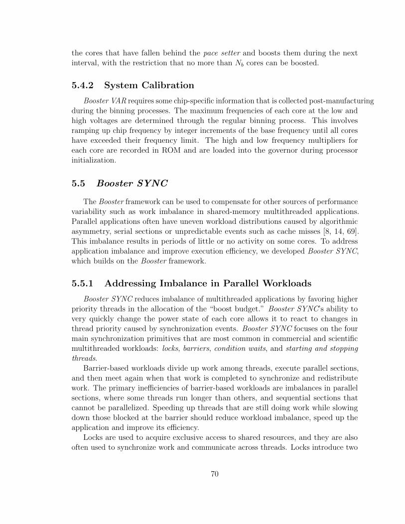
the cores that have fallen behind the pace setter and boosts them during the nextinterval, with the restriction that no more than Nb cores can be boosted.
5.4.2 System Calibration
Booster VAR requires some chip-specific information that is collected post-manufacturingduring the binning processes. The maximum frequencies of each core at the low andhigh voltages are determined through the regular binning process. This involvesramping up chip frequency by integer increments of the base frequency until all coreshave exceeded their frequency limit. The high and low frequency multipliers foreach core are recorded in ROM and are loaded into the governor during processorinitialization.
5.5 Booster SYNC
The Booster framework can be used to compensate for other sources of performancevariability such as work imbalance in shared-memory multithreaded applications.Parallel applications often have uneven workload distributions caused by algorithmicasymmetry, serial sections or unpredictable events such as cache misses [8, 14, 69].This imbalance results in periods of little or no activity on some cores. To addressapplication imbalance and improve execution e�ciency, we developed Booster SYNC,which builds on the Booster framework.
5.5.1 Addressing Imbalance in Parallel Workloads
Booster SYNC reduces imbalance of multithreaded applications by favoring higherpriority threads in the allocation of the “boost budget.” Booster SYNC’s ability tovery quickly change the power state of each core allows it to react to changes inthread priority caused by synchronization events. Booster SYNC focuses on the fourmain synchronization primitives that are most common in commercial and scientificmultithreaded workloads: locks, barriers, condition waits, and starting and stoppingthreads.
Barrier-based workloads divide up work among threads, execute parallel sections,and then meet again when that work is completed to synchronize and redistributework. The primary ine�ciencies of barrier-based workloads are imbalances in parallelsections, where some threads run longer than others, and sequential sections thatcannot be parallelized. Speeding up threads that are still doing work while slowingdown those blocked at the barrier should reduce workload imbalance, speed up theapplication and improve its e�ciency.
Locks are used to acquire exclusive access to shared resources, and they are alsooften used to synchronize work and communicate across threads. Locks introduce two
70

main ine�ciencies. The first is caused by resource contention, which can stall executionon multiple threads. Another potential ine�ciency occurs when locks are used forsynchronization. For instance, locks are sometimes used to implement barrier-likefunctionality, with the same ine�ciency issues as barrier. And locks are also often usedto serialize thread execution. Reducing time spent by threads in the lock’s “criticalsection” can potentially reduce both contention time and time spent in serializedexecution.
Condition waits are a form of explicit inter-process communication, where a threadblocks until some other thread signals for it to continue executing. Among other things,conditions are often used in producer-consumer algorithms, where the consumer blocksuntil the producer signals that there is input available. To improve performance,blocked threads can give up their boost budget to speed up active cores.
Finally, some workloads dynamically spawn and terminate worker tasks. A corethat is disabled because it has no task assigned is essentially the same as a core thatis blocked, although it is possible to save slightly more power by turning power o↵completely. The boost budget of inactive cores can be redistributed to those coresthat have work to do.
Unlike prior work that minimizes power for unbalanced workloads [8, 14, 69],our objective is to minimize runtime while remaining power-e�cient. Also, unlikeprior work we do not rely on criticality predictors to identify high-priority threads.Prediction would be too imprecise for lock and condition based workloads. Instead,Booster SYNC is a purely reactive system that uses hints provided by synchronizationlibraries and is managed by hardware to determine which cores are blocked and whichones are active.
5.5.2 Hardware-based Priority Management
Booster SYNC relies on hints from synchronization primitives to determine thestates of all threads currently running. We define the following priority states fora thread: blocked, normal, and critical. When a thread is first spawned, it is setto normal. If a thread reaches a barrier, and is not the last one, its state is set toblocked. If it is the last thread to arrive at the barrier, it sets the state of all the otherthreads to normal. Conditions work in a similar way, so if a thread is blocked on acondition, its state is blocked. Threads that receive the condition signal/broadcast areset to normal. When a thread attempts to acquire a lock, there are two possible statetransitions: if the thread acquires the lock, its state is set to critical, otherwise it is setto blocked. It is assumed that a critical section is likely to result in threads competingfor a shared resource. Speeding up critical threads should reduce contention time,thus speeding up the whole application. Finally, when a thread terminates while thereare no waiting threads in the run queue, a core will become idle and may be switchedo↵. Thread priority states and transitions are summarized in Table 5.1.
71

Thread Progress Thread Priority State
Thread spawned normalThread terminated none (core o↵)
Thread reaches barrier (not last) blockedLast thread reaches barrier normal (all threads)Lock acquire criticalLock release normalBlock on lock blocked
Block on condition blockedCondition signal normalCondition broadcast normal (all threads)
Table 5.1: Thread priority states set by synchronization events.
The Booster governor keeps track of thread priorities. The priority state of eachthread is stored as a 2-bit value in a Thread Priority Table (TPT) that is memory-mapped and accessible at process level. Priority tables are part of the virtual addressspace of each process, which allows any thread to change its own priority or thepriorities of other threads belonging to the same process. Frequently updated TPTentries are cached in the local L1 data caches of each CPU for quick access.
The governor maintains TPT entries coherent with a Core Priority Table (CPT),a centralized hardware table managed by the Booster governor and the OS. Notethat multiple independent parallel processes can run on the CMP at the same time.The CPT is used as a cache for the TPT entries corresponding to the threads thatare currently scheduled on the CMP, regardless of which process they belong to, asshown in Figure 5.3. Each CPT entry is tagged with the physical address of thecorresponding TPT entry and acts as a direct-mapped cache with as many entriesas there are processors in the system. Each entry contains the priority value for thethread running on the corresponding core. The CPT entries are maintained coherentwith local copies from each core through the standard cache coherence protocol.
5.5.3 SYNC Boosting Algorithm
Booster SYNC requires some minor changes to the boosting algorithm used inBooster VAR (Section 5.4.1). Just like in Booster VAR, the governor maintains a listof active cores sorted by core progress. In addition, Booster SYNC moves all criticalthreads to the head of the list. Given a “boost budget” of Nb cores Booster SYNCassigns the top Nb cores in the list to the high voltage rail. Cores that are in theblocked state are removed from the boost list and set to a low power mode (clockgated, on the low Vdd). Booster SYNC will accelerate only critical and normal threads.If many threads are blocked, fewer than Nb may be boosted.
72

1
3
2
1
1
1
1
1
1
2
1
3
...
...
Process 1
Process 2
Thread 1
Thread 2
Thread 3
Thread 1
Thread 2
Thread 3
Core PriorityTable (CPT)
(Core 0)
...
0 (Core N)
0xAAA76...80
Thread PriorityTable (TPT)
...
...
...
...
...
...
"Tag" (TPPhys. Addr.)
Process address spaces Hardware
0
1
2
Off
3
Normal
Blocked
Critical
Thread PriorityLegend
Figure 5.3: Thread Priority Tables are mapped into the process address space andcached in the Core Priority Table.
Booster SYNC uses the same core progress counters and metric as Booster VAR.However, progress of cores assigned blocked threads is accounted for di↵erently. Blockedcores are removed from the boost list and their progress counters are no longerincremented by the governor. As a result, the progress counters of cores emerging fromblocked states will indicate that they have fallen behind other cores. This would causeBooster to assign an excessive amount of boost to the previously-blocked threads. Toavoid this issue, whenever a core changes state from blocked to normal or critical, itsprogress counter is set to the maximum counter value of all other active cores. Thiswill place the core towards the bottom of the boost list.
5.5.4 Library and Operating System Support
Booster SYNC does not require special instrumentation of application software orspecial CPU instructions. Instead, it relies on modified versions of synchronizationlibraries that are typically supplied with the operating system, such as OpenMP andpthreads. To provide priority hints to the hardware, libraries write to entries in theTPT. When a running thread updates a local copy of a TPT entry, cache coherencewill ensure that the CPT is also updated. Note that hints could be implementedin the kernel instead of the synchronization library, but the kernel is typically notinformed as to which threads are holding locks (critical), limiting available TPT statesto normal and blocked.
During initialization, a process makes system calls to inform the OS as to whereits table entries are virtually located; the OS translates these into physical addressesand tracks this as part of the process and thread contexts. Association of TPT andCPT entries is also handled by the OS. On a context switch, the OS updates the CPTtag for each core with the physical address of the TPT entry of the corresponding
73

thread. The OS also guarantees protection and isolation for CPT entries belonging todi↵erent processes.
5.5.5 Other Workload Rebalancing Solutions
In our implementation, Booster uses cycle count as a metric of core progress. Thisallows Booster VAR to ensure that all cores execute the same number of cycles over afinite time interval. However, by altering the way we track core progress, we can usethe Booster framework to support other solutions for addressing workload imbalance.For instance, Bhattacharjee and Martonosi [8] observed that for instruction-count-balanced workloads, imbalance is caused by divergent L2 miss rates. Booster couldreduce this imbalance by using retired instruction count as the execution progressmetric. This will, in e↵ect, speed up threads that su↵er more long latency cache missesand help them keep up with the rest of the threads. Another alternative progressmetric might be explicit markers inserted by the programmer or compiler into theapplication, as in [14]. We leave detailed exploration of these approaches to futurework.
5.6 Evaluation Methodology
5.6.1 Architectural Simulation Setup
We used the SESC [103] simulator to model a 32-core CMP. Each core is a dual-issue out-of-order architecture. The Linux Threads library was ported to SESC inorder to run the PARSEC benchmarks that require the pthreads library. We ran thePARSEC benchmarks (blackscholes, bodytrack, fluidanimate, swaptions, dedup, andstreamcluster) and SPLASH2 benchmarks (barnes, cholesky, ↵t, lu, ocean, radiosity,radix, raytrace, and water-nsquared) with the sim-small and reference input sets.
We collected runtime and activity information, which we use to determine energy.Energy numbers are scaled for supply voltage, technology and variation parameters.
5.6.2 Delay, Power and Variation Models
For delay and power models, see Appendix A.We model variation in threshold voltage (Vth) and e↵ective gate length (Le↵) using
the VARIUS model [110]. We used the Markovic models to determine core frequenciesas a function of Vdd and Vth. To model the e↵ects of Vth variation on core frequency, wegenerate a batch of 100 chips that have di↵erent Vth (and Le↵) distributions generatedwith the same mean and standard deviation. This data is used to generate probabilitydistributions of core frequency at nominal and near threshold voltages.
To keep simulation time reasonable, we ran the microarchitectural simulationsusing four random normal distributions of core Vth with a standard deviation of 12%
74

CMP architectureCores 32, out-of-orderFetch/issue/commit width 2/2/2Register file size 76 int, 56 fpInstruction window 56 int, 24 fpL1 data cache 4-way 16KB, 1-cycle accessL1 instruction cache 2-way 16KB, 1-cycle accessDistributed L2 cache 8-way 8MB, 10 cycle accessTechnology 32nmCore, L1 Vdd 400-600mVCore, L1 frequency 300-2300MHz, 25MHz incrementsL2, NoC Vdd 400mVL2, NoC frequency 400MHzVariation parametersVth mean (µ), 210mVVth std. dev./mean (�/µ) 12%
Table 5.2: Summary of the experimental parameters.
over the nominal Vth. All core and cache frequencies are integer multiples of a 25MHzreference clock. The L2 cache and NoC are on the lower voltage rail, with operatingfrequencies constrained accordingly. We ran all experiments with each frequencydistribution, and we report the arithmetic mean of the results.
Table 5.2 summarizes the experimental parameters.
5.7 Evaluation
We evaluate the performance and energy benefits of eliminating core-to-corefrequency variation with Booster VAR and reducing application imbalance withBooster SYNC. We compare the e↵ectiveness of Booster VAR to a mechanism thatmitigates frequency variation through thread scheduling similar to the ones in [100, 123].We also compare Booster SYNC with an ideal implementation of Thrifty Barrier [69].
We begin by evaluating the e↵ects of process variation on core frequency at lowvoltage.
5.7.1 Frequency Variation at Low Voltage
Low-voltage operation increases the e↵ects of process variation dramatically. Usingour variation model, we examine within-die frequency variation at both nominal(900mV) and near threshold Vdd (400mV). In Figure 5.4 we show core-to-core variationin frequency as a probability distribution of core frequency divided by die mean(average over all cores in the same die). The distributions shown are for 9% and
75

Vth �/µ Freq. �/µ at 900mV Freq. �/µ at 400mV3% 1.0% 7.5%6% 2.1% 15.1%9% 3.2% 22.8%
12% 4.4% 30.6%
Table 5.3: Frequency variation as a function of Vth �/µ and Vdd.
0
0.002
0.004
0.006
0.008
0.01
0.012
0 0.5 1 1.5 2
Prob
abili
ty d
istri
butio
n
Relative frequency
900mV, Vth �/µ= 9%900mV, Vth �/µ=12%400mV, Vth �/µ= 9%400mV, Vth �/µ=12%
Figure 5.4: Core-to-core frequency variation at nominal and near-threshold Vdd, relativeto die mean (average over all cores in the same die).
12% within-die Vth variation. At nominal Vdd the distribution is relatively tight, withonly 4.4% frequency standard deviation divided by the mean (�/µ). At low voltage,frequency variation is 30.6% �/µ with cores deviating from less than half to morethan 1.5⇥ the mean. Table 5.3 summarizes the impact of di↵erent amounts of Vth
variation on frequency �/µ.The high within-core variation deteriorates CMP frequency significantly. In the
absence of variation, a 32nm CMP at 400mV would be expected to run at about400MHz. At the same Vdd, a 12% Vth variation would bring the average frequencyacross all dies to 149MHz, assuming each die’s frequency is set to that of its slowestcore.
To avoid the severe degradation in CMP frequency, each core can be allowed torun at its best frequency, resulting in a heterogeneous CMP. However, the randomnature of variation-induced heterogeneity can still lead to poor and unpredictableperformance.
5.7.2 Workload Balance in Parallel Applications
The way in which parallel applications handle workload partitioning has a directimpact on their performance when running on heterogeneous vs. homogeneous CMPs.
76

Broadly speaking, parallel applications divide work either statically at compile timeor dynamically during execution.
Static Load Partitioning
Statically partitioned workloads are generally designed for homogeneous systems.Significant e↵ort goes into making sure work assignment is as balanced as possible. Ingeneral, well-balanced workloads are expected to perform poorly on heterogeneousCMPs because their performance is limited by the slowest core. For instance, eachthread of ↵t executes the same algorithm and processes the same amount of data. Aslow thread bottlenecks the performance of the entire application. These applicationsshould benefit from the performance homogeneity of Booster VAR.
Many applications like lu, radix, and dedup are inherently unbalanced due toalgorithmic characteristics. In theory, these applications could perform well onheterogeneous systems if critical threads are continuously matched to fast cores. Inpractice, their performance is unpredictable, especially when running on systems withvariation-induced heterogeneity. These are the types of applications we expect willbenefit most from Booster SYNC.
Dynamic Load Balancing
Some applications, like radiosity and raytrace, employ mechanisms for dynamicallyrebalancing workload allocation across threads. Dynamic load balancing is beneficialwhen the runtime of individual work units is highly variable. These applications adaptwell to performance-heterogeneous systems. As a result, we expect them to benefitlittle from the Booster framework.
We summarize in Table 5.4 the relevant algorithmic characteristics of all bench-marks we simulated. We include the expected benefits from Booster VAR and BoosterSYNC. For applications like radix, water-nsquared, fluidanimate and bodytrack, eventhough they are either statically partitioned and balanced, or use dynamic load balanc-ing, some benefit from Booster SYNC is still possible. This is because the applicationsinclude some amount of serialization in the code or have a serial master thread thatcan be sped up by Booster SYNC.
5.7.3 Booster Performance Improvement
We evaluate the performance of Booster VAR and Booster SYNC relative to aheterogeneous baseline in which each core runs at its best frequency. Figure 5.5 showsthe execution times of all benchmarks normalized to the baseline (“Heterogeneous”).The target frequency for Booster is chosen to match the average frequency of theheterogeneous baseline.
77
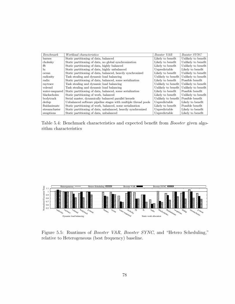
Benchmark Workload characteristics Booster VAR Booster SYNCbarnes Static partitioning of data, balanced Likely to benefit Unlikely to benefitcholesky Static partitioning of data, no global synchronization Likely to benefit Unlikely to benefitfft Static partitioning of data, highly balanced Likely to benefit Unlikely to benefitlu Static partitioning of data, highly unbalanced Unpredictable Likely to benefitocean Static partitioning of data, balanced, heavily synchronized Likely to benefit Unlikely to benefitradiosity Task stealing and dynamic load balancing Unlikely to benefit Unlikely to benefitradix Static partitioning of data, balanced, some serialization Likely to benefit Possible benefitraytrace Task stealing and dynamic load balancing Unlikely to benefit Unlikely to benefitvolrend Task stealing and dynamic load balancing Unlikely to benefit Unlikely to benefitwater-nsquared Static partitioning of data, balanced, some serialization Likely to benefit Possible benefitblackscholes Static partitioning of work, balanced Likely to benefit Unlikely to benefitbodytrack Serial master, dynamically balanced parallel kernels Unlikely to benefit Possible benefitdedup Unbalanced software pipeline stages with multiple thread pools Unpredictable Likely to benefitfluidanimate Static partitioning of work, balanced, some serialization Likely to benefit Possible benefitstreamcluster Static partitioning of data, unbalanced, heavily synchronized Unpredictable Likely to benefitswaptions Static partitioning of data, unbalanced Unpredictable Likely to benefit
Table 5.4: Benchmark characteristics and expected benefit from Booster given algo-rithm characteristics
0.5
0.6
0.7
0.8
0.9
1
1.1
radiosity
raytrace
volrend
bodytrack
g.meanbarnes
oceanwater-nsquared
cholesky
fft lu radixblackscholes
fluidanimate
swaptions
dedupstreamcluster
g.mean
No
rmal
ized
Ex
ecu
tio
n T
ime
Dynamic load balancing Static work allocation
Heterogeneous Hetero Scheduling Booster VAR Booster SYNC
Figure 5.5: Runtimes of Booster VAR, Booster SYNC, and “Hetero Scheduling,”relative to Heterogeneous (best frequency) baseline.
78

We also compare Booster VAR and Booster SYNC to a heterogeneity-awarethread scheduling approach, “Hetero Scheduling,” that dynamically migrates slowthreads to faster cores and short-running threads to slower cores. This techniqueis similar to those used to cope with heterogeneity in [100] and [123], but we applyit to multithreaded workloads. In our implementation, migration occurs at barriersynchronization points using thread criticality information collected over the previoussynchronization interval. We chose an ideal implementation of “Hetero Scheduling”that introduces no performance penalty from thread migration, except when causedby incorrect criticality prediction from one barrier to the next.
Booster VAR improves the performance of workloads that use static work allocationby an average of 14% compared to the baseline. “Hetero Scheduling” also performsbetter than the baseline for statically scheduled workloads but reduces execution timeby only 5%. As expected, workloads that use dynamic rebalancing adapt well toheterogeneity and have no performance benefit from Booster VAR or from “HeteroScheduling.” Booster VAR is especially beneficial for balanced workloads such as ↵t,blackscholes or water-nsquared that are hurt by heterogeneity. “Hetero Scheduling,”on the other hand, can do little to help these cases.
Booster SYNC builds on the Booster VAR framework, allocating the boost budgetto critical or active threads. This leads to significant performance improvements, evenfor workloads where Booster VAR is ine↵ective. For statically partitioned workloadswith significant imbalance, such as dedup, swaptions or streamcluster, Booster SYNCimproves performance between 15% and 20%. Booster VAR brings no performancegains for these applications. Booster SYNC also helps some dynamically balancedapplications that have significant serialization due to resource contention, such asbodytrack, by boosting their critical sections.
Balanced applications like ↵t, blackscholes and water-nsquared, which benefitsignificantly from Booster VAR, have little or no additional performance gains fromBooster SYNC. Overall, Booster SYNC complements Booster VAR very well. Onaverage, it is 22% faster than the baseline for static workloads and 9% faster fordynamic workloads.
Impact of Di↵erent Synchronization Primitives
Figure 5.6 shows the e↵ects of Booster SYNC responding to hints from di↵erentsynchronization primitives in isolation, for a few benchmarks. lu is a very unbalancedbarrier-based workload. Providing the Booster governor with hints about barrieractivity speeds up the application by 24% over Booster VAR. Information about locks,conditions or thread spawning does not help speed up lu. bodytrack makes heavyuse of locks, with a substantial amount of contention. Speeding up critical sectionsresults in a 17% speed increase over Booster VAR. Boosting cores that are not blockedon condition waits also helps. swaptions uses no synchronization at all but insteadactively spawns and terminates worker threads. As a result, it benefits greatly from
79

0.5
0.6
0.7
0.8
0.9
1
1.1
lu bodytrack swaptions
No
rmal
ized
Ex
ecu
tio
n T
ime
Booster VARBarriers
Locks
ConditionsNo Task
Booster SYNC (All)
Figure 5.6: Booster SYNC performance impact of using hints from di↵erent types ofsynchronization primitives in isolation.
0
0.2
0.4
0.6
0.8
1
1.2
1.4
radiosity
raytrace
volrend
bodytrack
g.mean
barnesocean
water-nsquared
cholesky
fft lu radixblackscholes
fluidanimate
swaptions
dedupstreamcluster
g.mean
No
rmal
ized
En
erg
y x
Del
ay
Dynamic load balancing Static work allocation
Heterogeneous Thrifty Barrier Booster VAR Booster SYNC
Figure 5.7: Energy⇥delay for Booster VAR, Booster SYNC, and ideal Thrifty Barrier,relative to Heterogeneous (best frequency) baseline.
providing the Booster governor with information about active thread count, whichallows the redistributing of boost budget from unused cores. This speeds up swaptionsby 15% over Booster VAR.
5.7.4 Booster Energy Delay Reduction
We examine the energy implications of Booster VAR and Booster SYNC comparedto the baseline. Figure 5.7 shows the energy delay product (ED) for each benchmark.We compare with an ideal implementation of “Thrifty Barrier” [69], which puts coresinto a low-power state when they reach a barrier, with no wakeup time penalty.
Booster VAR generally uses more power than the “Heterogeneous” baseline in orderto achieve homogeneous performance at the same average frequency. As a result, EDis actually higher than the baseline for the dynamically balanced workloads. However,for statically partitioned benchmarks, Booster VAR lowers ED by 11%, on average.Booster SYNC is much more e↵ective at reducing energy delay because in addition tospeeding up applications, it saves power by putting inactive cores to sleep. It achieves
80
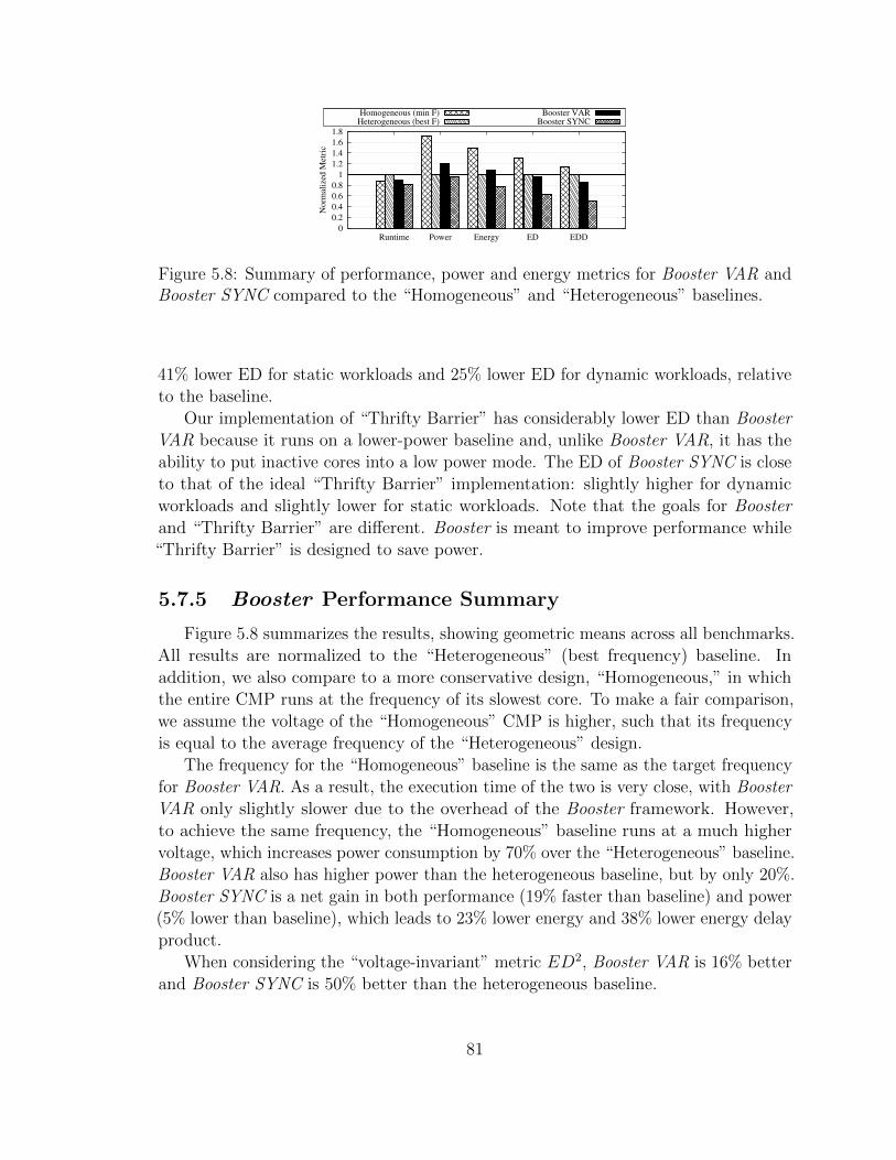
0
0.2
0.4
0.6
0.8
1
1.2
1.4
1.6
1.8
Runtime Power Energy ED EDD
No
rmal
ized
Met
ric
Homogeneous (min F)Heterogeneous (best F)
Booster VARBooster SYNC
Figure 5.8: Summary of performance, power and energy metrics for Booster VAR andBooster SYNC compared to the “Homogeneous” and “Heterogeneous” baselines.
41% lower ED for static workloads and 25% lower ED for dynamic workloads, relativeto the baseline.
Our implementation of “Thrifty Barrier” has considerably lower ED than BoosterVAR because it runs on a lower-power baseline and, unlike Booster VAR, it has theability to put inactive cores into a low power mode. The ED of Booster SYNC is closeto that of the ideal “Thrifty Barrier” implementation: slightly higher for dynamicworkloads and slightly lower for static workloads. Note that the goals for Boosterand “Thrifty Barrier” are di↵erent. Booster is meant to improve performance while“Thrifty Barrier” is designed to save power.
5.7.5 Booster Performance Summary
Figure 5.8 summarizes the results, showing geometric means across all benchmarks.All results are normalized to the “Heterogeneous” (best frequency) baseline. Inaddition, we also compare to a more conservative design, “Homogeneous,” in whichthe entire CMP runs at the frequency of its slowest core. To make a fair comparison,we assume the voltage of the “Homogeneous” CMP is higher, such that its frequencyis equal to the average frequency of the “Heterogeneous” design.
The frequency for the “Homogeneous” baseline is the same as the target frequencyfor Booster VAR. As a result, the execution time of the two is very close, with BoosterVAR only slightly slower due to the overhead of the Booster framework. However,to achieve the same frequency, the “Homogeneous” baseline runs at a much highervoltage, which increases power consumption by 70% over the “Heterogeneous” baseline.Booster VAR also has higher power than the heterogeneous baseline, but by only 20%.Booster SYNC is a net gain in both performance (19% faster than baseline) and power(5% lower than baseline), which leads to 23% lower energy and 38% lower energy delayproduct.
When considering the “voltage-invariant” metric ED2, Booster VAR is 16% betterand Booster SYNC is 50% better than the heterogeneous baseline.
81

5.8 Conclusions
This chapter presents Booster, a simple, low-overhead framework for dynamicallyreducing performance heterogeneity caused by process variation and applicationimbalance. Booster VAR completely eliminates core-to-core frequency variationresulting in improved performance for statically partitioned workloads. BoosterSYNC reduces the e↵ects of workload imbalance, improving performance by 19% onaverage and reducing energy delay by 23%.
Acknowledgements
This work was supported in part by the National Science Foundation under grantCCF-1117799 and an allocation of computing time from the Ohio SupercomputerCenter. The authors would like to thank the anonymous reviewers for their valuablefeedback and suggestions, most of which have been included in this final version.
82

CHAPTER 6
VRSync: Synchronization-Induced Voltage Emergencies
6.1 Motivation and Main Idea
Low-voltage systems have an increased sensitivity to voltage fluctuations. Thesefluctuations are caused by abrupt changes in power demand triggered by processoractivity variation with workload. If the voltage deviates too much from its nominalvalue, it can lead to so-called “voltage emergencies,” which can cause timing violationsand memory retention errors in the processor. To prevent these emergencies, chipdesigners add voltage margins that in modern processors can be as high as 20%[50, 102], leading to higher power consumption than necessary.
Previous work [33, 34, 35, 36, 52, 96, 101, 102] has proposed several hardwareand software mechanisms for reducing the slope of current changes (dI/dt), whichdampens voltage fluctuations. This allows the use of smaller voltage guardbands,saving substantial amounts of power. All previous work, however, has focused onsingle-core [33, 35, 36, 52, 96, 101] or low core-count systems [33, 102].
As technology scales and the number of cores in future CMPs increases, the e↵ectsof chip-wide activity variation will overshadow the e↵ects of within-core workloadvariability. The power demand of individual cores will account for a much smallerfraction of the chip’s total power consumption. As a result, core-local activity is lesslikely to cause large power fluctuations that lead to emergencies. However, chip-widecoordinated activity such as that forced by global synchronization in multithreadedapplications leads to much larger and rapid power fluctuations. For instance, barriersynchronization causes blocked threads to idle with very low power consumption.When all idle threads are released from a barrier the associated jump in activity acrossall cores leads to very large power spikes that can lead to voltage emergencies. Goingforward, we will need to rethink the mechanisms used to avoid voltage emergencies toensure they are e↵ective and energy-e�cient as the number of cores continues to scale.
This chapter characterizes voltage variability in large CMPs running at low voltages.We find that, in a 32-core CMP running multithreaded benchmarks, the most severevoltage droops are associated with thread synchronization primitives such as barriersand, to a lesser extent, with other thread activity such as new thread spawning. We
83

find that about half of the benchmarks tested (a mix of SPLASH2 and PARSECapplications) trigger multiple emergencies in system with a typical 10% voltageguardband.
Starting from this observation, we propose VRSync, a voltage-aware synchroniza-tion methodology that controls thread activity in critical scenarios. For example,VRSync enforces the gradual release of threads from barriers, leading to a gradualincrease in power consumption. This limits the amplitude of the largest voltage droops,avoiding emergencies with smaller guardbands. VRSync is a software-only solutionthat can be implemented in system-level synchronization libraries and/or the OS.VRSync eliminates all emergencies in the benchmarks we test, allowing for a lowervoltage guardband. A CMP with VRSync and a small guardband uses 33% less energythan a system that uses voltage guardbanding alone to eliminate emergencies. Theruntime overhead of VRSync varies greatly with the density of synchronization andother application behavior, but averages about 6%.
Overall, this chapter makes the following contributions:
• Analyzes the e↵ects of thread synchronization on supply voltage stability. To thebest of our knowledge, this is the first work to identify synchronization events asa major source of severe voltage droops in large CMPs. These observations arevalidated with power measurements from a 4-core, Intel Core i7 system.
• Shows that synchronization-induced emergencies are more likely as the number ofcores increases.
• Presents VRSync, a novel synchronization methodology that prevents voltageemergencies, allowing smaller guardbands and saving energy.
• Evaluates VRSync using a commercial regulator model.
6.2 Background
Prior work has focused on addressing voltage emergencies in low core count systems.Reddi et al. [101] proposed a solution for eliminating emergencies in single-core CPUs.They employ heuristics and a learning mechanism to predict voltage emergencies fromarchitectural events. When an emergency is predicted, execution rate is throttled,reducing the slope of current changes. Gupta et al. [36] proposed an event guidedadaptive voltage emergency avoidance scheme: Recurring emergencies are avoidedby initiating various operations such as pseudo-nops, prefetching, and a hardwarethrottling mechanism on events that cause emergencies. Gupta et al. also proposedDeCoR [35], a checkpoint/rollback solution which allows voltage emergencies butdelays the commit of instructions until they are considered safe. A low voltage sensor,of known delay, signals that an emergency is likely to have occurred and the pipelineis flushed and rolled back to a safe state.
Powell and Vijaykumar [96] proposed two approaches for reducing high-frequencyinductive noise caused by processor pipeline activity. Pipeline mu✏ing reduces the
84

number of functional units switching at any given time by controlling instruction issue.A priori current ramping slowly ramps up the current of functional units before theyare utilized in order to reduce the amplitude of the current surge.
A software approach to mitigating voltage emergencies was proposed by Gupta etal. in [34]. They observe that a few loops in SPEC benchmarks are responsible forthe majority of emergencies in superscalar processors. Their solution involves a set ofcompiler-based optimizations that reduce or eliminate architectural events likely tolead to emergencies such as cache or TLB misses and other long-latency stalls.
Very few previous studies have examined voltage emergencies in multicore chips.Gupta et al. [33] characterize within-die voltage variation using a detailed distributedmodel of the on-chip power-supply grid. They model a 4-core CMP and use a multi-programmed workload consisting of SPEC applications in their evaluation. Reddiet al. [102] evaluate voltage droops in an existing dual-core microprocessor. Theypropose designing voltage margins for typical instead of worst-case behavior, relyingon resilience mechanisms to recover from occasional errors. They also propose co-scheduling threads with complementary noise behavior, to reduce voltage droops. Weare not aware of any previous work that examines voltage emergencies in CMPs withlarge numbers of cores running multithreaded applications as we do in this work.
A significant amount of recent work has demonstrated dramatic power savingsfrom low voltage operation. These works aggressively scale supply voltage to veryclose to the threshold voltage [77, 18, 27, 84, 85]. In general, two orders of magnitudepower savings are possible with an order of magnitude reduction in frequency. Overallthe technology promises an order of magnitude reduction in energy. Many challengesremain, including reliability and high variation. Achieving low voltage operationrequires significant reduction in voltage margins that can only be achieved if othertechniques for reducing voltage droops are developed.
6.3 Power Delivery and Regulation
Power to a modern CPU is delivered and controlled by a voltage regulator circuit.The regulator performs two main functions: It steps down the supply voltage to thelevel required by the CPU, and it keeps the voltage stable under varying current loads.Regulation is typically achieved by charging a capacitor on a duty cycle, using a lowpass RLC filter to integrate the resulting voltage. The regulator monitors the outputvoltage and compares it to a reference voltage. When deviations occur (e.g. due to achange in load) it adjusts the duty cycle to maintain a stable output voltage.
6.3.1 Voltage Droops
Regulators are designed to respond quickly and precisely to changes in currentloads, to prevent voltage fluctuations outside a narrow band around the nominal
85
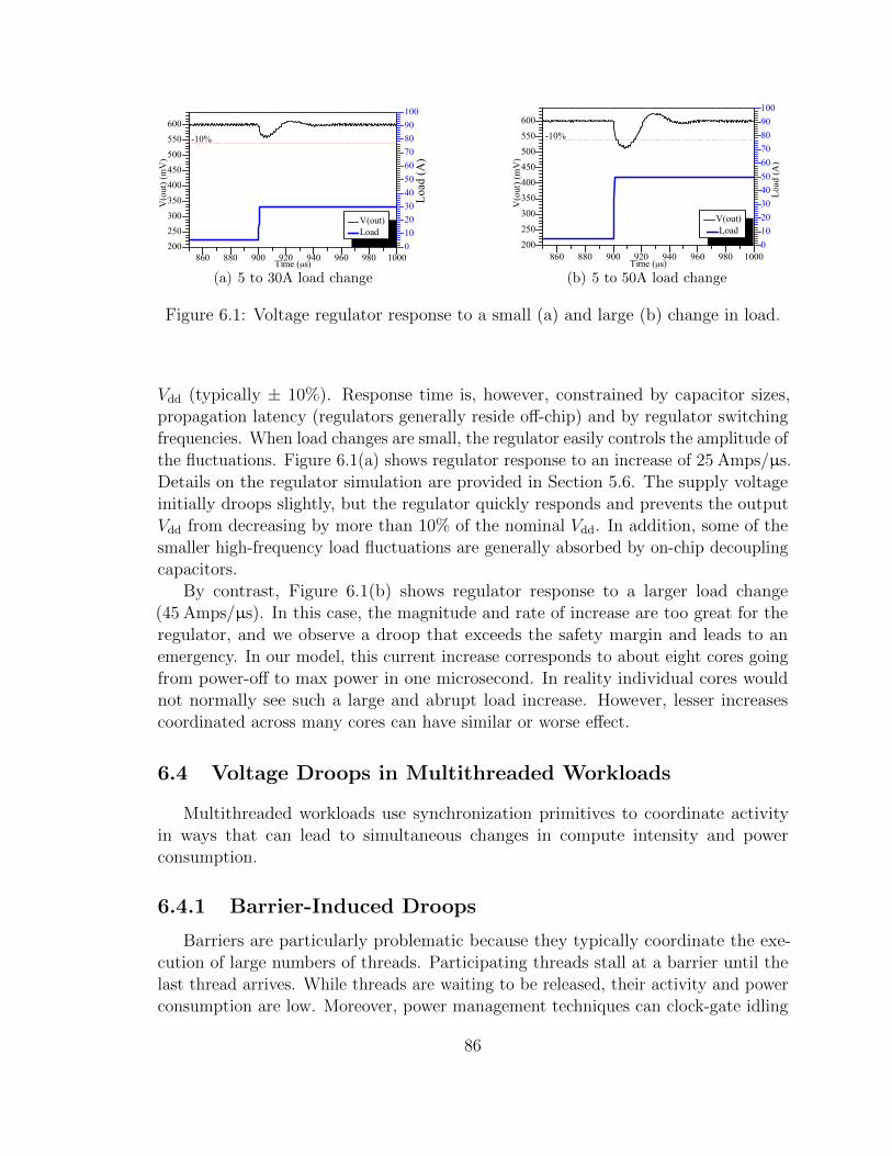
860 880 900 920 940 960 980 1000200250300350400450500550600
V(out) Load
Time (µs)
-10%
V(o
ut) (
mV
)
0102030405060708090100
Loa
d (A
)
(a) 5 to 30A load change
860 880 900 920 940 960 980 1000200250300350400450500550600
V(o
ut) (
mV
)
-10%
Time (µs)
0102030405060708090100
V(out) Load
Loa
d (A
)
(b) 5 to 50A load change
Figure 6.1: Voltage regulator response to a small (a) and large (b) change in load.
Vdd (typically ± 10%). Response time is, however, constrained by capacitor sizes,propagation latency (regulators generally reside o↵-chip) and by regulator switchingfrequencies. When load changes are small, the regulator easily controls the amplitude ofthe fluctuations. Figure 6.1(a) shows regulator response to an increase of 25 Amps/µs.Details on the regulator simulation are provided in Section 5.6. The supply voltageinitially droops slightly, but the regulator quickly responds and prevents the outputVdd from decreasing by more than 10% of the nominal Vdd. In addition, some of thesmaller high-frequency load fluctuations are generally absorbed by on-chip decouplingcapacitors.
By contrast, Figure 6.1(b) shows regulator response to a larger load change(45 Amps/µs). In this case, the magnitude and rate of increase are too great for theregulator, and we observe a droop that exceeds the safety margin and leads to anemergency. In our model, this current increase corresponds to about eight cores goingfrom power-o↵ to max power in one microsecond. In reality individual cores wouldnot normally see such a large and abrupt load increase. However, lesser increasescoordinated across many cores can have similar or worse e↵ect.
6.4 Voltage Droops in Multithreaded Workloads
Multithreaded workloads use synchronization primitives to coordinate activityin ways that can lead to simultaneous changes in compute intensity and powerconsumption.
6.4.1 Barrier-Induced Droops
Barriers are particularly problematic because they typically coordinate the exe-cution of large numbers of threads. Participating threads stall at a barrier until thelast thread arrives. While threads are waiting to be released, their activity and powerconsumption are low. Moreover, power management techniques can clock-gate idling
86

0
10
20
30
40
50
60
70
80
90
100
100 120 140 160 180 200 220 240
0
1
2
3
4
Po
wer
(W
atts
)
Co
res
in B
arri
er
Time (milliseconds)
Cores in BarrierPower (Watts)
Figure 6.2: Processor power consumption while running the PARSEC benchmarkfluidanimate on a 4-core Intel Core i7 system.
cores [8, 69] further reducing their power consumption. When idle threads are finallyreleased from the barrier, cores typically experience a surge of activity, causing a spikein current demand and power consumption, which can lead to a voltage emergency.
Figure 6.2 shows the power consumption for a 4-core Intel Core i7 processorrunning the PARSEC benchmark fluidanimate with 4 working threads and the sim-large input set. The trace was obtained using Intel’s Running Average Power Limit(RAPL) interface [45] that provides access to an internal energy counter updated everymillisecond. The counter tallies the energy expended by the 4 cores but excludes the“un-core” components such as the on-chip memory controller. In addition to power, thefigure also shows how many threads (cores) are blocked at a barrier at any given time.The figure captures one of the “frames” in the fluidanimate benchmark which includeseight barriers. In most cases, as cores arrive at a barrier, the power consumption dropsfollowed by a significant spike. This is evident for all the barriers except the first andlast ones, which occur during (or before) low-power serial sections. The power spikesare quite severe in some cases – for instance following barrier #5 – and can lead tovoltage emergencies.
In this experiment synchronization events are not the only triggers of significantpower fluctuations. We can observe other significant spikes that are likely causedby other architectural events such as long latency cache misses followed by burstsof activity. This behavior is consistent with that observed in previous work thatexamined voltage emergencies in 2-core [102] or 4-core [33] CMPs. Those studies didnot single out synchronization events as a significant source of voltage emergencies.
6.4.2 Impact of Core Count on Voltage Droops
Core counts are likely to continue to increase for the foreseeable future. We thereforeexamine the e↵ects of synchronization events on power fluctuation in processors with
87

Po
wer
(W
atts
)
Co
res
in B
arri
er
Time (milliseconds)
Cores in BarrierPower (Watts)
0
10
20
30
40
50
60
70
30 40 50 60 70 80 0
1
2
3
4
(a) 4 cores
Po
wer
(W
atts
)
Co
res
in B
arri
er
Time (milliseconds)
Cores in BarrierPower (Watts)
0
10
20
30
40
50
60
70
30 35 40 45 50 55 60 65 70 0
2
4
6
8
(b) 8 cores
Po
wer
(W
atts
)
Co
res
in B
arri
er
Time (milliseconds)
Cores in BarrierPower (Watts)
0
10
20
30
40
50
60
70
36 38 40 42 44 46 48 50 0
8
16
24
32
(c) 32 cores
Figure 6.3: Power variation for fluidanimate on CMP configurations with: (a) 4 cores,(b) 8 cores and (c) 32 cores.
larger numbers of cores. We run the same application (fluidanimate) on simulatedmany-core systems with 4, 8 and 32 cores, increasing the number of threads to matchthe number of cores. To provide a fair comparison of the relative magnitude of thevoltage fluctuations, all systems are scaled to have the same maximum power (TDP).To keep simulation time reasonable, we use the sim-small reference input set. Detailsabout the experimental methodology are provided in Section 5.6.
We find that the number of cores in the CMP has a direct impact on the magnitudeof the power fluctuations caused by synchronization events, relative to those causedby core-level activity variation. Figure 6.3 shows the power profile for the three runs.Figure 6.3(a) shows that, for the 4-core case, the power profile follows that observed inthe native execution (Figure 6.2). The simulation shows more local variability becausethe simulation models power at cycle granularity while the native execution can onlybe sampled every millisecond. Some of the power spikes correlate well with barrieractivity. However, other local events are also causing significant fluctuations, justlike in the native run. The ratio between the amplitude of the power spikes causedby barriers and non barrier-related events over the same time interval is close to 1,meaning they are equally likely to lead to emergencies.
However, as the core count increases, within-core workload variability has a lowerimpact on chip-level power consumption. Events that trigger power fluctuations withinindividual cores are less likely to occur simultaneously on multiple cores and, as aresult, their e↵ects on power variability will tend to cancel each other out. This isvisible in Figure 6.3(b), which shows power consumption when running on an 8-coreconfiguration. Compared to the 4-core configuration, the benchmark exhibits lessvariability in power in sections of the application without barrier activity. However,around barriers, power fluctuations are much higher. The ratio between the barrier andnon-barrier related spikes is closer to 3 in this case. This trend becomes significantlymore pronounced for 32 cores (Figure 6.3(c)) with barrier-induced power spikes 6⇥larger than non barrier-related spikes. This trend suggests that, in the large CMPs
88

0 10 20 30 40 50 60 70 80 90
100 110
0 10 20 30 40 50 60 70 80 0
8
16
24
32
Po
wer
(W
atts
)
Co
res
in B
arri
er
Time (milliseconds)
Cores in BarrierPower (Watts)
(a) barnes
Figure 6.4: Power variation in response to barrier synchronization for barnes.
of the near-future, coordinated activity fluctuation across many cores is much morelikely to lead to voltage emergencies than within-core workload variability.
We have observed a similar behavior in most of the barrier-based benchmarks weexamined. Figure 6.4 shows the power profile for barnes (a SPLASH2 application)running on 32 cores. barnes displays a very strong correlation between barrier syn-chronization and variation in power consumption. For instance, as cores start to reachthe first barrier, there is a gradual decrease in power consumption. When the barrieris exited, power consumption spikes, likely leading to a voltage emergency. Laterbarriers are entered a lot more rapidly by all threads, which causes sharp drops inpower consumption, followed by spikes when they are released.
6.4.3 Other Voltage Droop-Causing Events
A condition signal broadcast has the potential to wake up many waiting threadssimultaneously. We treat this as a special case of barrier synchronization, althoughnone of our workloads have demonstrated this problem.
Lock synchronization does not generally cause the type of activity coordinationthat can lead to large power fluctuations. Even if a large number of threads arecontending for a lock, they will acquire it sequentially, thus avoiding the activity spiketypical for barriers. In our workloads we did not observe any emergencies that couldbe attributable directly to lock activity.
In addition to synchronization, some thread management functions can lead tolarge activity variation in parallel applications. These applications often create a setof worker threads during initialization, which are usually launched all at once. In thiscase, thread spawning can have an e↵ect similar to barrier exit.
Active power management such as clock or power-gating can significantly reducepower consumption of idle threads. This can make voltage droops worse because the
89

power fluctuation when transitioning into active state will generally be higher than ifpower management was not employed.
6.5 VRSync Design and Implementation
In order to eliminate synchronization induced voltage emergencies we developVRSync, a novel synchronization methodology that controls core activity while inbarriers and during barrier exit. We also apply VRSync to control the timing of threadspawning at the OS level.
6.5.1 Barrier Implementation
To reduce cache coherence tra�c, we use a hierarchical barrier based on a binarysoftware combining tree [83, 133]. In our implementation, a node is dynamicallyassigned to each participating thread. Each node has a sense flag that only its childrenobserve while blocked on the barrier. The last thread to enter the barrier is assignedto the root node, at which time it inverts its sense flag to release waiting threads. Itschildren observe this and invert their sense flags, propagating this wake-up signal downthe tree and releasing all threads from the barrier. The barrier tree is implemented asa one-dimensional array indexed by node numbers. This allows threads to locate theirassigned node data structures in constant time, without traversing the tree. Arrayelements (including the sense flag variables) are allocated such that they will map todi↵erent cache lines, to avoid false sharing.
Threads are assigned nodes based on the order they enter the barrier (from highestnumbered node to lowest). Node numbers are computed from a shared variable c,which is atomically incremented by each thread, starting from zero. Given a nodenumber i, its parent node is p = b(i� 1)/2c, its left child is l = 2i+ 1, and its rightchild is r = 2i+ 2. With n cores participating in the barrier, i = n� 1� c, so thatfor 32 cores, the first to enter the barrier is assigned node i = 31 and the last one isassigned node i = 0.
6.5.2 Scheduled Barrier Exit
VRSync implements a scheduled barrier exit to prevent the high current surgesassociated with barrier release. The schedule ramps up thread activity more slowly,leading to a more gradual rate of increase in power consumption. In VRSync threadsparticipate in the barrier in two phases. The first is the blocked phase, prior to thetime when all threads have arrived at the barrier. Cores assigned to blocked threadssleep or busy-wait in a way that minimizes power. Once all threads have arrived,threads enter the delayed phase. Cores assigned delayed threads continue to sleepuntil a thread-local timer has expired. We examine two exit schedules (Linear and
90

First enterExecution
Blocked on barrier 1 Delay
Blocked on barrier 2 Delay
All in barrier 1All in barrier 2
T0
T7
Linear schedule
t7
T1T2T3T4T5T6
Time
Thre
ads
(a) Linear exit schedule
First enterExecution
Blocked on barrier 1All in barrier
Delay
All outT0
T7
Thre
ads
T1T2T3T4T5T6
Time
(b) Bulk exit schedule
0 50 100 150 200 250 300400
450
500
550
600
650
700
V(out) No. of active cores
-10%
V(o
ut) (
mV
)
time (µs)
04812162024283236
No.
of
activ
e co
res
(c) VR response to Linear exit
0 50 100 150 200 250 300400
450
500
550
600
650
700
V(out) No. of active cores
-10%
time (µs)
V(o
ut) (
mV
)
04812162024283236
No.
of a
ctiv
e co
res
(d) VR response to Bulk exit
Figure 6.5: Timing diagrams and VR response to the Linear exit schedule (a), (c) andthe Bulk exit schedule (b), (d).
Bulk) that control the pattern and rate at which cores are allowed to leave the delayedphase.
Linear Exit Schedule
The Linear schedule simply adds a fixed progressive delay to the wake-up of eachthread that participates in a barrier. Figure 6.5(a) shows an example of the Linear exitschedule for 8 threads participating in two barriers. The first barrier phase proceeds asin a regular barrier. However, when the last thread reaches the barrier, all threads arereleased from the blocked phase (essentially clearing the barrier) and move into thedelayed phase. The threads are scheduled to exit the delayed phase in the reverse orderof their arrival. This is done as an optimization, to ensure that critical threads (thosethat arrive last at the barrier) will be released first. The assumption is that thesethreads are likely to remain critical for subsequent barriers, and giving them higherexit priority should improve performance. In Figure 6.5(a), thread T0 is the last toarrive at the first barrier and will be the first one to leave. The release of the rest ofthe threads is delayed by a delay unit relative to the release of the previous thread.The value of the delay unit is conservatively chosen to be the minimum the processorcan tolerate without experiencing an emergency under worse-case load conditions.
91

Figure 6.5(c) illustrates the e↵ect of the Linear schedule on the stability of theoutput voltage for a 32-core processor. It shows the output voltage over time, ascores are gradually turned on. This experiment assumes cores are initially o↵ andwill consume maximum power when on, although in reality, the power increase willbe less. The Linear schedule gradually ramps up demand on the voltage regulator,which keeps the voltage droop above the safe margin of ±10%. A more rapid ramp-upin demand would trigger a response similar to that in Figure 6.1(b), leading to anemergency.
Bulk Exit Schedule
The Linear barrier exit schedule is relatively easy to test and implement. However,because voltage regulators have a non-linear response to transient workloads, it mightbe suboptimal. The speed of the regulator response depends on a number of factorsincluding the quality of the control loop and the size of inductors and capacitors. TheVR responds to a voltage droop by “pumping” additional current into the processor.The response however is not instantaneous. If the VR is given some time to catch upwith the new demand, it might be able to respond faster to subsequent load increases.
We take advantage of the VR non-linearity with an alternative barrier exit schedule,called Bulk, which provides a faster exit compared to Linear. In the Bulk schedule,cores are released from the barrier in batches rather than one at a time. After a batchof cores is released, the VR is given some time to respond, followed by another batch,until all cores have exited the delayed phase of the barrier. Figure 6.5(b) shows anexample with 8 threads leaving a barrier on the Bulk schedule. Figure 6.5(d) illustratesthe VR response to a Bulk release of six cores at a time for a 32-core chip. ComparingFigures 6.5(c) and 6.5(d) we can see that the initial droop for the Bulk schedule issteeper but shorter, so it doesn’t trigger an emergency. Because the load changeis abrupt the VR responds aggressively to raise the voltage, which allows a secondbatch of six cores to be released without causing an emergency. Overall, the Bulk exitschedule completes about 20% faster than the Linear schedule for the same load.
6.5.3 Early Exit in Overlapping Barriers
Some applications make very heavy use of barrier synchronization, and their runtimecould be hurt substantially by the delayed exit schedules. In heavily synchronizedapplications, barriers are often very closely spaced, with only a few instructionsbetween them. As a result it is not uncommon for barriers to be “overlapping,” withsome threads exiting one barrier and entering a second before other threads haveexited the first. VRSync makes overlapping barriers more likely because of the unequaldelay it introduces in the exit time of each thread. A thread that enters the secondbarrier will rapidly go into a lower power state, reducing the load on the regulator. Inthis case, the scheduled barrier exit is unnecessarily conservative because it assumes
92

Old schedule
T0
T7
New schedulet0 t1 t2t3 t4 t5 t6
Barrier 1 Barrier 2
T1T2T3T4T5T6
Thre
ads
Time
(a) Timing diagram for 8 threads, early exit.
T33
T44
T55
T7 6
1 T2
2
0
T0 7
b d b d b d b d
b d b d
b d
b d [#] - Node Number[b] - Blocked[d] - Delayed
(b) Barrier tree state at time t3.
Figure 6.6: Example of early exit from the Linear schedule due to overlapping barriers.
all cores will consume peak power until the scheduled exit is complete. To eliminatethe unnecessary overhead we would like to allow threads to exit the delayed phase ofthe barrier early. For instance, when a thread goes to block on the second barrier itcould signal to another delayed thread that it can leave its delayed phase early.
Figure 6.6(a) shows an example of early exit applied to the Linear schedule. Inthis example thread T0 is last to reach the first barrier at time t1 and will thereforebe the first scheduled to exit. When T0 enters the second barrier at time t2 it willtrigger the early exit of thread T7 at time t3. If there were no barrier overlap, T7would have stayed in the delayed phase of the barrier until time t5. The same patternrepeats until all threads exit the first barrier. This occurs much earlier (t4) than thelinear exit schedule would have dictated (t5).
To implement the early exit schedule we add an early wake variable to each nodein the barrier tree. A thread entering the barrier will set this flag. If another threadis in the delayed phase on the same node, it will detect this flag change and exitimmediately. Figure 6.6(b) shows the state of the barrier tree for the example inFigure 6.6(a), at time t3. At that time, thread T0 has left the first barrier, arrived atthe second barrier and been assigned to node 7. Before T0 goes into the blocked state,it wakes up thread T7, which was in delayed state at node 7. T7 goes on to block onnode 6, waking up T6. At time t3, threads T2 through T5 are in the delayed phase ofthe first barrier on nodes 2 to 5. Threads T1 and T6 are in execution between thetwo barriers and do not occupy any node in the tree at time t3.
6.5.4 VRSync Implementation
VRSync is implemented as a user-level library that provides emergency-free syn-chronization and is installed system-wide. To implement the scheduled exit, VRSyncrequires a core-local timestamp, such as a cycle counter, which is used to time wakefrom the delayed barrier phase. The wake time is calculated, and a spin-wait executes
93

until that time is reached. To implement spin-wait in a power-e�cient manner thelibrary uses a PAUSE instruction, like what was introduced to x86 processors in the SSE2instruction set. On a PAUSE instruction, the CPU front-end inserts a long delay beforefetching the next instruction, thereby significantly reducing the IPC and dynamicpower of the core.
OS-Level VRSync
An OS-level VRSync implementation is also needed to prevent emergencies thatcan be caused by thread spawning or non-VRSync synchronization. These eventsinvolve OS interaction and must therefore be handled at OS-level. In essence, the OSmust ensure that emergencies are not triggered when work is scheduled to cores thathave been previously idle or sleeping. New work is assigned to idle cores by issuingan interrupt to these cores. The interrupt can come from another thread (spawn) orfrom a hardware device (I/O). VRSync augments this mechanism by scheduling corewake-up according to the Linear or Bulk schedules, avoiding emergencies.
The same OS-level implementation ensures that applications using standard syn-chronization instead of the VRSync library will not trigger voltage emergencies. Mostbarrier primitives use blocking calls handled by the OS. When threads are releasedfrom a standard barrier, they appear to the OS as core-wakeup events. Since these arescheduled by the OS-level VRSync, they will not cause emergencies. However, userswill have an incentive to use the VRSync library instead of standard synchronizationfor performance reasons. The OS implementation of VRSync has a higher overheadthan the library, and it cannot take advantage of performance optimizations like earlyexit for overlapping barriers. As we show in Section 5.7, these optimizations canreduce the overhead of VRSync by as much as 25⇥.
VRSync Design Parameters
The parameters chosen for the Linear and Bulk exit schedules of VRSync aredependent on the regulator design, size of capacitors, number of regulator phases, etc.They are also dependent on the desired safety margins and the power characteristicsof the cores. These parameters would therefore need to be determined by processormanufacturers. Since processors and voltage regulators are often developed by di↵erentmanufacturers, data from regulator data sheets or manufacturer-supplied models canbe used to perform the necessary design-time simulations. Once the parametersare chosen, they can be programmed in the system firmware and accessed by thesynchronization libraries.
To determine these design parameters, we simulate a commercial regulator fromLinear Technologies [74] using LTspice [75] and a manufacturer supplied model. Wemeasure regulator response to load changes, assuming worst-case power consumptionfor each core. For the Linear schedule, multiple simulations are run with di↵erent
94

CMP architectureCores 32, out-of-orderFetch/issue/commit width 2/2/2Register file size 76 int, 56 fpInstruction window 56 int, 24 fpL1 data cache 4-way 16KB, 2-cycleL1 instruction cache 2-way 16KB, 2-cyclePrivate L2 8-way 256KB, 10-cycleNoC Interconnect 2D TorusCoherence L2-level, MESITechnology 22nmVdd 600mVClock Frequency 1GHz
Table 6.1: Summary of the experimental parameters.
delay values until the minimum value that does not cause an emergency is found.Similarly, for Bulk we determine the optimal number of cores that can be releasedtogether and the delay between bulk exits.
6.6 Evaluation Methodology
6.6.1 Architectural Simulation Setup
Most of our experiments are conducted on a simulated 32-core CMP in 32nmtechnology using SESC [103]. Each core is a dual-issue out-of-order architecture.SESC was modified to run a port of the LinuxThreads library, a simple implementationof POSIX Threads required by the PARSEC benchmarks. We collected runtime andenergy information. Table 6.1 summarizes the architecture configuration.
We ran the PARSEC benchmarks blackscholes, bodytrack, fluidanimate, swaptions,dedup, and streamcluster and the SPLASH2 benchmarks barnes, cholesky, ↵t, lu,ocean, radiosity, radix, raytrace, and water-nsquared with the reference, sim-smallinput sets. The benchmark sets include applications with light, moderate and veryheavy barrier activity as well as applications that use no barriers. Most applicationsuse at least some lock synchronization and some of the PARSEC benchmarks usecondition waits.
To model power consumption at low voltage we used the models from Markovicet al. [77]. (For details, see Appendix A.) These were integrated into CACTI [93] toextract energy per access for all the SRAM memory structures including register file,caches, etc. The low voltage models were also used to scale the existing SESC powermodel for logic units. To model NoC power we used Orion 2 [53].
95

6.6.2 Voltage Regulator Simulation Setup
For this work, we used a state of the art voltage regulator, Linear Technology’sLTC3729L-6 polyphase, synchronous step-down switching regulator [74]. This is acommercially-available regulator intended for use in desktop computers and servers.The regulator’s behavior is simulated in LTspice IV [75] using a model provided bythe manufacturer. We set up the LTC3729L-6 in a 6 phase design, which requires 3LTC3729L-6 chips with 12 onboard capacitors of 270 µF each and a combined ESRof 2 mOhms. The controllers are synchronized using the CLKOUT pin of the firstchip. Figure 6.7 shows the circuit diagram for two of the regulator phases. The inputvoltage was set at 12V and the output voltage set at 600mV by means of a resistordivider circuit using remotely sensed output voltage. The regulator configuration andcapacitor values were chosen to provide the maximum current required (160 Amps)for low-Vdd operation, in line with Intel specifications [46]. The regulator drives acurrent sink that models the processor load.
The current traces obtained from the SESC simulator were fed into the regulatorto measure the regulator response to a wide range of load steps and various load slews.We measured the regulator response to a sweep of current changes and identifiedthe maximum rate at which load can change without causing an emergency (MaxdI/dt). We define a voltage emergency as occurring if the output voltage droops below10% of the target voltage. While this margin is consistent with industry practicesand previous work, it is the result of a tradeo↵ between power consumption goals,component (e.g. capacitors, controllers) cost and size, etc.
We use Max dI/dt to identify emergencies in the power consumption profileextracted from the microarchitectural simulator. Changes in current that exceed MaxdI/dt are flagged as emergencies. Parameters for the Linear and Bulk exit schedulesare determined using VR simulations, based on worst-case assumptions about powerconsumption. Once delay schedules are determined, they are programmed into ourVRSync implementation in the simulator.
6.7 Evaluation
In this section we analyze the incidence of voltage emergencies across di↵erentmulti-threaded applications and the e↵ectiveness of VRSync at eliminating them. Wealso evaluate the impact of the VRSync Linear and Bulk policies on execution timeand energy.
The evaluation includes two baseline systems. The more conservative baseline usesno active power management, meaning that when blocked on a barrier, threads willsimply issue a PAUSE instruction that will reduce the IPC and power of the busy-waitloop. The second baseline employs active power management through clock-gating atcore level. When blocked, threads execute a HALT instruction, which cuts the core’sdynamic power.
96

Figure 6.7: Diagram of the voltage regulator circuit design (two of the six phases).
6.7.1 Voltage Emergencies
We analyze power traces obtained from simulator runs to identify voltage emergen-cies. These are defined as voltage droops larger than 10%, which would be triggeredby current changes that exceed Max dI/dt. Table 6.2 shows the results of this study.For each benchmark we show both the number of dynamic barriers and the numberof emergencies for the two baseline runs. In general, the number of emergenciescorrelates very well with the number of barriers. For instance ocean has a very largenumber of barriers and also experiences the largest number of voltage emergencies.This correlation however doesn’t always hold. streamcluster has extremely heavybarrier activity, yet it registers no emergencies. This is likely due to the fact thatstreamcluster has relatively low IPC and low maximum power consumption. As aresult, when threads exit from barriers their activity does not increase su�ciently tocause emergencies.
Table 6.2 also shows the number of emergencies that occur in the baseline systemthat uses clock gating. The number of emergencies increases for most benchmarks.This is because cores idle with lower power while blocked at a barrier, leading tohigher power spikes upon exit. For ocean the number of emergencies increases byalmost 30%.
Eliminating Emergencies with VRSync
Figure 6.8(a) shows an example of a barrier that leads to an emergency in fluidan-imate. We show power consumption over time, the number of threads in a barrier atany given time and the location of emergencies (red arrow, at the top of the graph).We can see that as threads enter the barrier, power consumption gradually drops,
97

Benchmark Num. ofNumber of emergencies
BaselineBaseline w/ VRSync VRSync
barriers clock gating Linear Bulk
radiosity 10 0 1 0 0barnes 17 0 0 0 0ocean 900 419 543 0 0raytrace 1 0 0 0 0water-nsq’d 20 7 10 0 0cholesky 4 0 0 0 0↵t 7 8 8 0 0lu 67 50 56 0 0radix 11 2 3 0 0blackscholes 1 0 0 0 0bodytrack 80 0 0 0 0fluidanimate 24 9 10 0 0swaptions 0 9 9 0 0dedup 0 0 0 0 0streamcluster 4396 0 0 0 0
Table 6.2: Number of barriers and number of emergencies for the baseline system, thebaseline with clock gating and for VRSync Linear and Bulk. VRSync eliminates allemergencies for clock-gated and non-clock-gated cases.
followed by a big spike upon exit. Soon after, threads enter a second barrier, but thisone does not lead to an emergency.
Figure 6.8(b) shows the e↵ect of the Linear schedule on the same section of thebenchmark. This schedule leads to a more gradual resumption of compute activity,which eliminates the emergency. This example illustrates the e↵ects of the overlappingbarrier optimization which allows early exit from the first barrier as threads enter thesecond one.
Figure 6.8(c) shows the e↵ects of the Bulk schedule on the same code. We can seethat the exit from the barrier now occurs in batches of threads, leading to a step-wise,but still gradual ramp-up in power. Again, the emergency is avoided. The Bulk exit isalso faster than the Linear one, but both are slower than the baseline.
Figure 6.9 shows the power profiles for lu, ↵t and swaptions. Figure 6.9(a) showslu running on the baseline with no clock gating. For lu, emergencies are perfectlycorrelated with barrier exits. Because of high activity following the barriers, almostall barrier exits lead to emergencies. Figure 6.9(d) shows that the Bulk scheduleeliminates all emergencies with a slight increase in execution time.
In some cases, program phases can remain highly synchronized long after thesynchronization event has completed. This occurs in parallel workloads with verybalanced workload distribution across threads. An example of this behavior can
98

Po
wer
(W
atts
)
Co
res
in B
arri
erTime (milliseconds)
Emergency
EmergencyCores in Barrier
Power (Watts)
0
10
20
30
40
50
60
70
80
90
46.98 47 47.02 47.04 47.06 0
8
16
24
32
(a)P
ow
er (
Wat
ts)
Co
res
in B
arri
er
Time (milliseconds)
EmergencyCores in Barrier
Power (Watts)
0
10
20
30
40
50
60
70
80
90
49.44 49.47 49.5 49.53 49.56 49.59 0
8
16
24
32
(b)
Po
wer
(W
atts
)
Co
res
in B
arri
er
Time (milliseconds)
EmergencyCores in Barrier
Power (Watts)
0
10
20
30
40
50
60
70
80
90
49.38 49.41 49.44 49.47 49.5 49.53 0
8
16
24
32
(c)
Figure 6.8: Power variation in response to synchronization for a barrier from fluidani-mate: (a) baseline without clock gating (b) Linear barrier exit schedule and (c) Bulkexit schedule.
Po
wer
(W
atts
)
Co
res
in B
arri
er
Time (milliseconds)
EmergencyCores in Barrier
Power (Watts)
0 10 20 30 40 50 60 70 80 90
32 34 36 38 40 42 0
8
16
24
32
(a) lu, baseline
Pow
er (
Wat
ts)
Core
s in
Bar
rier
Time (milliseconds)
EmergencyCores in Barrier
Power (Watts)
0 10 20 30 40 50 60 70 80 90
0 0.1 0.2 0.3 0.4 0.5 0.6 0
8
16
24
32
(b) ↵t, baseline
Po
wer
(W
atts
)
Co
res
in B
arri
er
Time (milliseconds)
EmergencyCores in Barrier
Power (Watts)
0 10 20 30 40 50 60 70 80 90
0.2 0.3 0.4 0.5 0.6 0.7 0.8 0.9 1 0
8
16
24
32
(c) swaptions, baseline
Po
wer
(W
atts
)
Co
res
in B
arri
er
Time (milliseconds)
EmergencyCores in Barrier
Power (Watts)
0 10 20 30 40 50 60 70 80 90
32 34 36 38 40 42 44 0
8
16
24
32
(d) lu, Bulk
Po
wer
(W
atts
)
Co
res
in B
arri
er
Time (milliseconds)
EmergencyCores in Barrier
Power (Watts)
0 10 20 30 40 50 60 70 80 90
0 0.1 0.2 0.3 0.4 0.5 0.6 0.7 0.8 0.9 0
8
16
24
32
(e) ↵t, Linear
Po
wer
(W
atts
)
Co
res
in B
arri
er
Time (milliseconds)
EmergencyCores in Barrier
Power (Watts)
0 10 20 30 40 50 60 70 80 90
0.2 0.3 0.4 0.5 0.6 0.7 0.8 0.9 1 0
8
16
24
32
(f) swaptions, Bulk threadspawn
Figure 6.9: Power profile for lu, ↵t and swaptions for the baseline without clock gating(a), (b), (c), for the Bulk (d), and Linear (e) schedules, and for scheduled spawn only(f).
99

be seen in Figure 6.9(b), which shows power consumption for ↵t. This workload ischaracterized by alternating periods of high and low IPC (due to phases of low andhigh last-level cache misses), and these periods occur nearly simultaneously across allthreads, even though no synchronization is present. These synchronous fluctuationslead to multiple emergencies. Figure 6.9(e) shows how the Linear exit schedulesignificantly diminishes these power fluctuations. This happens because the Linearrelease schedule realigns threads relative to each other leading to less overlap in thehigh and low activity phases, completely eliminating emergencies from ↵t.
All emergencies in swaptions are caused by simultaneous spawning of large numbersof threads. Figure 6.9(c) shows a short section of the application startup. Severalemergencies occur early on in the execution. All of these are eliminated by the VRSyncscheduled thread spawn as Figure 6.9(f) shows.
6.7.2 VRSync Impact on Execution Time
VRSync delayed exit can impact execution time because it forces threads to spendadditional time in barriers. Figure 6.10 shows the execution time of all benchmarksfor the Linear and Bulk exit schedules with and without the early exit optimization.
As expected, the Linear schedule has the highest overhead, with an average increasein execution time of 11% across all the benchmarks. Applications that have moderateto no barrier activity have very small increase in runtime, between 0 and 10%. ↵tis an exception because, even though it has few barriers, its runtime is very short,making barrier exit schedules a significant fraction of its runtime.
Applications with heavy barrier activity su↵er significantly more from VRSync.streamcluster has by far the highest overhead, with a 2.1⇥ increase in execution time.The high overhead is due to the very large number of barriers (4396) used by thisbenchmark. ocean has the second largest overhead (62%), again because of the largenumber of barriers (900).
The Bulk schedule reduces the average execution time overhead to 6.3%. Stream-cluster shows a dramatic improvement with just over 36% overhead compared to 100%with the Linear schedule. This is due to the interplay between the exit schedule andthe early exit optimization. The Bulk schedule releases multiple threads right at thebarrier exit, which quickly reach a new barrier, triggering early exit sooner than in theLinear case. Overlapping barriers with early exit are very common in streamcluster.
The early exit optimization has a very big impact on the performance of VRSyncin benchmarks with large numbers of barriers. As Table 6.3 shows, without early exit,the runtime overhead would be as high as 3.36⇥ for ocean and as high as 24.9⇥ forstreamcluster. The average runtime overhead for Bulk without early exit would beclose to 35% for instead of 6.3% with early exit.
Barnes, raytrace, and dedup actually speed up slightly. When parallel taskssimultaneously go through periods of high memory activity, they compete for memory
100

0
0.2
0.4
0.6
0.8
1
1.2
1.4
1.6
radiositybarnes
oceanraytrace
water-nsquared
choleskyfft lu radix
blackscholes
bodytrackfluidanimate
swaptions
dedupstreamcluster
g.mean
Norm
aliz
ed E
xec
uti
on T
ime
2.1
LinearBulk
Figure 6.10: VRSync execution times for Linear and Bulk schedules, normalized tobaseline.
No overlap No overlapBenchmark Linear Linear Bulk Bulk
ocean 1.62 3.36 1.50 2.96streamcluster 2.10 24.90 1.36 16.75g.mean (ALL) 1.11 1.39 1.06 1.35
Table 6.3: Runtimes (relative to baseline) for ocean, streamcluster, and the geometricmean over all benchmarks. For these benchmarks, the overlapping barrier optimizationis critical for good performance.
bandwidth and slow each other down. VRSync shifts the alignment of those phases,reducing competition for shared resources and making execution more e�cient.
6.7.3 VRSync Energy
We examine the energy implications of using the proposed VR-aware schedulingversus other options for avoiding voltage emergencies. Table 6.4 summarizes theresults. Each entry in the table shows the average runtime, power and energy for thedi↵erent techniques relative to a baseline without clock gating. Because the baselinehas no barrier exit scheduling and a small guardband, it cannot avoid emergencies.
Another option for eliminating voltage emergencies is to increase the voltageguardband, while using faster versions of VRSync. Bulk 160mV shows a combinationof higher guardband with the Bulk scheduling policy. The voltage guardband for thethis option increases from 60mV to 160mV . This allows for a faster exit schedulethat the regular Bulk schedule, reducing the runtime overhead. However, because thesupply voltage is higher, energy consumption increases by 42%. Note that even withthe higher guardband VRSync is still needed to guarantee emergency-free execution.
101

Technique Guardband Schedule Emergencies Runtime Power Energy
Baseline 60mV (None) yes 1.0 1.0 1.0VRSync Linear 60mV Linear no 1.112 0.98 1.086VRSync Bulk 60mV Bulk no 1.063 0.99 1.049
Bulk 160mV 160mV Bulk no 1.045 1.361 1.422Optimistic 210mV (None) no 1.0 1.563 1.563guardband
Table 6.4: The e↵ects of di↵erent guardbands on average benchmark execution time,power, energy, and emergencies.
We also define a guardband-only option, which we call Optimistic guardband,based on our workloads. We identified the steepest dI/dt of any of our benchmarksand determined the necessary safe voltage guardband to avoid emergencies withoutVRSync. The Optimistic guardband case would increase energy by 56% over baseline.
From the summary in Table 6.4 we can see that the most energy e�cient optionfor avoiding voltage emergencies is VRSync Bulk with only 4.9% increase in energyover a baseline with emergencies. This solution also uses only 67% of the energy of aCMP with the Optimistic guardband needed to eliminate voltage emergencies.
6.8 Conclusion and Future Work
Market and technology factors are driving CPU architects to employ increasinglyaggressive energy and power-saving design techniques. Lowering supply voltage makeschips more susceptible to the e↵ects of severe supply voltage fluctuations, which canlead to errors. In this paper we identify an important problem that will challengefuture low-voltage CMPs. We show that in large systems, voltage emergencies will becaused almost exclusively by coordinated activities across many cores, such as barriersynchronization, where multiple cores experience sudden changes in compute demandsimultaneously. We propose a set of low overhead and highly e↵ective techniques formitigating these challenges. Unlike previous work, our solutions are deterministic anddo not rely on heuristics for predicting when voltage emergencies are likely to occur.
We hope this work will inspire future research on this topic. One aspect we wouldlike to address is the impact of multiple voltage domains on voltage emergencies.Future CMPs with hundreds of cores are likely to have cores organized into clusters,with each cluster receiving an independently regulated voltage supply. Voltage droopscaused by cross-domain workload migration and other aspects related to multiplevoltage domains will have to be investigated. In this work we showed how clock gatingcan be a significant source of voltage droops. In future work we will investigate the
102

impact of other power management techniques, such as core-level power gating, onvoltage stability.
103

CHAPTER 7
Related Work
Our research depends heavily on a large body of prior work that pertains totechnology scaling trends and challenges. As transistors shrink, they become lessreliable and harder to predict. Power density is increasing, but simple solutions likelowering supply voltage have the potential to exacerbate these problems. Among thechallenges being faced are process variation, errors (transient and permanent), andenergy reduction. Below is a cross-section of recent research.
7.1 Process Variation
7.1.1 Process Variation in Logic
Borkar and colleagues have done a great deal of work on process variation. A 2003[11] paper covers the e↵ects of and some solutions for variation on 90nm geometryand smaller. At nominal voltages, they observe die-to-die 20x variation in leakagecurrent and 30% variation in frequency, accompanied by a high degree of within-dieleakage variation in the faster chips. Besides threshold voltage (Vth) variation, [11]observes that leakage variation is also further impacted by temperature variation. Thetemperature variation is caused, in part, by nonuniformity in the kinds of logic foundat di↵erent places on a chip. Di↵erent logic components will have di↵erent switchingactivity levels, causing hot spots, which leak more. And changes in switching activitycause fluctuations in supply voltage over time to di↵erent logic components. Parametervariation, Voltage variation, and Temperature variation are the main problems dealtwith by this paper. This paper and [126] suggest bidirectional (forward or backward, asneeded) adaptive body bias as a means to deal with leakage (during idle periods) andperformance (during active periods). Voltage fluctuations (spatially and temporally)and hotspots are mitigated by adaptive frequency throttling and adaptive supplyvoltage. Teodorescu et al. in [122] introduce a dynamic fine-grained body biasingtechnique for mitigating within-die variation, increasing processor frequency andreducing power.
104

VARIUS [121, 110] is a landmark paper that provides a general model of systematicprocess variation in microprocessors. Consistent with empirical data, a Sphericalcorrelation structure is used to generate realistic maps of systematic threshold voltageand e↵ective channel length for within-die variation. The parameters for this modelare mean and standard deviation of parameter variation and the correlation betweenpoints as a function of distance. Using this model, VATS is developed to predict theprobability of timing errors in logic circuits.
ReVIVaL [72] is a very fine grained, dual-supply-voltage technique for mitigatingsystematic variation e↵ects. A processor’s clock frequency is limited by the delaythrough its slowest pipeline stage. ReVIVaL equalizes the delay through pipelinesin di↵erent functional units and processor cores on a die through a combination ofvoltage interpolation and time borrowing. Time borrowing is a technique for allowinga pipeline stage to take more than a whole clock period to function. The clock to theinput pipeline register can be advanced, and/or the clock to the output register can bedelayed. However, this “borrows” time from the adjoining stages. Slow pipeline stagescan be sped up by switching them to a higher supply voltage, and fast stages canbe slowed (to save energy) by switching to a lower supply voltage. For a sequence ofpipeline stages, the e↵ective supply voltage can be set between the two available railsby connecting alternating stages to each supply, much like dithering. Additionally,pipelines can be provided with an optional “dummy” pipeline stage that is used to takeup extra slack from time borrowing. With particularly slow sections of a chip, theseextra stages can be enabled, inserting an additional cycle of latency, while allowingthe clock rate to remain high. ReVIVaL is an enhancement over ReCycle [124], whichprovides time borrowing and donor stages but only a single voltage supply.
[43] addresses core-to-core variation in CMPs. At a single supply voltage, eachcore will have a di↵erent best frequency. If each core has its own clock, this leadsto performance asymmetry, which has negative consequences for parallel workloads.Slowing all cores to the speed of the slowest core wastes power and performance in thefaster cores. In order to level the frequency variation, adaptive voltage scaling (AVS)and adaptive body bias (ABB) are explored. AVS is found to be better than ABBbecause AVS requires smaller adjustments in voltage for a given change in speed, andAVS has a smaller impact on leakage.
Dynamic logic is a circuit technique, based primarily on N-type transistors, thatexploits the transient characteristics of circuit elements in order to perform compu-tation. Unlike the more familiar static logic, dynamic logic does not have a directlow-impedance path from power or ground to the output, instead relying on the lowphase of the clock to precharge (or setup) a circuit and the high phase of the clockfor computation (or evaluation). Dynamic circuits exploit transistor load capacitanceto hold state, and since the state held in the capacitor will decay quickly, dynamiccircuits have a minimum clock rate. Dynamic circuits can be up to twice as fastas static circuits, but they typically require more transistors and more power. A
105

common solution to the minimum clock rate problem is the use of a “keeper” elementthat maintains state beyond the usual decay period. Dynamic circuits are subjectto the same process variation e↵ects as static circuits, and this is the subject of [56].Rather than a static keeper, a tunable keeper is employed, in conjunction with aleakage current sensor. Circuits with higher leakage (lower Vth), are also faster andcan function adequately with a weaker keeper. This dynamic solution combats thee↵ects of variation, leading to reduced static power, reduced delay variation, andhigher performance. This paper relies on an earlier paper by the same authors [55]that focuses specifically on the design of the leakage sensor.
Because of the unpredictability of variation, it is often necessary to measurecircuit delay characteristics of a device post-manufacturing. Straightforward solutionsinvolve adding test circuits (e.g. ring oscillators). [64] presents an alternative basedon compressed sensing that performs analog timing tests on circuits that are alreadypart of the functional design of the IC. A circuit path is sensitizable if there exists atest vector that will allow its propagation delay to be tested. Compressed sensing [23]is a method for reconstructing an x 2 Rm vector from n < m linear measurements ifthere is a known transformation in the domain from Rm to Rn, such as when x is asparse vector or can be approximated by a sparse vector. Using compressed sensing,[64] makes reliable estimates of delay variation in a circuit, using less than exhaustivetesting of sensitizable paths in the circuit.
Most solutions to process variation rely either on post-manufacturing testing orgeneral statistical models. By contrast, [76] accounts for variation by making it afirst-class design consideration. This approach uses knowledge about process variationto guide a designer’s microarchitectural choices primarily in the areas of pipeline depth,logic depth, and circuit activity that a↵ects temperature. For instance, increasinglogic depth reduces critical path delay variation.
7.1.2 Process Variation in Memories
Although most transistors in a 32nm design have 32nm channel length, channelwidth (as a design parameter) is adjusted as necessary for performance. Widertransistors are faster, because they can conduct more current. Since logic is typicallydesigned for performance, the widest transistors are used, and one e↵ect of this isthat logic transistors are a↵ected much more by systematic variation than by randomvariation. Static RAMs, on the other hand, are highly area constrained, and switchingspeed of transistors within bit cells is of diminished importance. (Performance inRAMs is primarily a function of the decoder circuitry.) Thus, SRAMs use the smallesttransistors, and as a result, they are a↵ected significantly by both systematic andrandom variation.
As transistors shrink, SRAM cells su↵er from an ever-increasing failure rate. Readand write failures occur due to imbalance between the back-to-back inverters, and
106

access failures occur due to slowness or failure of the access transistors. Because ofthese failures, SRAMs are typically designed with some form of over-provisioning.Extra rows and/or columns in the RAM array are provided that can be statically ordynamically substituted in place of those that have failed. With small geometry andlow voltage designs, in the face of higher variation, cell failure rates are very high,and simple over-provisioning has reached its limit as a practical solution. The relatedworks in this area provide various clever solutions to this problem.
A variation-aware cache architecture is proposed in [1]. In this design, a cachewith faulty cells is dynamically resized. In a direct-mapped cache, the index portionof an address maps to a unique location in the cache. Part of that index is the rowaddress, which selects the word line to activate. And part of the index is the columnaddress, which controls a multiplexer that selects among the bit lines. When oneof the columns has a faulty bit, the proposed design will force the column MUX tochoose a di↵erent, non-faulty column. Because this now maps more than one block tothe same location, the column bits must be stored in the tag array. When reading, thecolumn address is compared against the tag, and a mismatch results in a cache miss.Although the average cache capacity is reduced, yield is increased from 33% to 93%.
[16] addresses the SRAM transistor variation problem for sub-threshold designs.In order to ensure that standard 6-transistor (6T) SRAM cells operate reliably andhave a low failure rate at ultra-low voltage, constituent transistors must be increasedin size. Calculations are performed to determine the necessary area. Then a 10T cellis proposed as a substitute. Although this cell would be larger for nominal voltagedesigns, the required size increase is less for reliable operation in sub-threshold. Thus,if a particular capacity of sub-threshold SRAM composed of 6T cells were redesignedwith 10T cells, it would be smaller, use less energy, and have a lower minimum supplyvoltage. Similarly, [19] explores an 8T cell that reduces energy and area requirementsfor iso-robustness with 6T cells at near threshold.
[71] proposes a solution to within-die variation by introducing variable-latencystructures. In the case of register files, registers are divided into fast entries, which canbe accessed in a single cycle, and slow entries, which require additional access time.Register files are typically multi-ported, and di↵erent ports will have di↵erent delaysfor the same registers; this is exploited in combination with the previous techniquein order to increase clock rate with minimal reduction in IPC. For multi-stage logicpipelines, variable latency is provided using time borrowing and an additional optionalpipeline stage.
107

7.2 Faults and Error Correction
7.2.1 Transient Logic Error Correction
Mitra and colleagues are known for their work on soft errors. Soft errors (alsoreferred to as Single Event Upsets) are a type of transient logic level inversion causedby radiation particle strike. Soft errors can cause incorrect calculation in logic andincorrect data stored in memory. A 2006 paper [89] presents two mechanisms for miti-gating soft errors in combinational logic. With “Error Correction using Duplication,”combinatorial logic is replicated, with the outputs of twin logic components connectedto a circuit (C-element) that retains the previously-known value when the two inputshave opposite values. This eliminates transient logic level glitches caused by particlestrikes. This is costly in terms of area, so they also introduce some partial replicationtechniques, along with “Error Correction using Time-shifted Outputs.” With thelatter, a delay element is inserted so that the C-element receives both a delayed andnon-delayed version of the output from a single logic circuit. As long as the durationof the glitch is shorter than the delay imposed, this technique can correct soft errors.However, this technique may increase clock cycle period by as much as that of thedelay element.
It is useful to quantify the vulnerability of a circuit to soft errors, and this is done in[91], which introduces the Architectural Vulnerability Factor (AVF). Based on circuitstructure and activity analysis, it can be determined which signal paths are more orless likely to a↵ect the final result of any computation. It is then possible to estimatean expected rate of actual errors from the raw environmental soft error rate and alogic component’s AVF. While [91] focuses on a static AVF model, [129] introducesa workload-dependent component. Many soft error detection solutions provide fullredundancy, either by replicating hardware or replicating instructions. Some workloads,however, may not require this level of replication of all logic components in order toremain resistant to soft errors, and [129] provides a method for dynamically disablingunnecessary redundancy, in order to save energy. Finally, [114] examines how softerror rates have progressed with shrinking transistor technologies and predicts howthose trends will continue in the future.
Developed by Ernst et al., Razor [31] is a particularly famous and well-citedtechnique for mitigating timing errors in combinatorial logic. In a typical logic circuitdesign, supply voltage is raised or clock frequency is lowered in order to provide a“guard band” against supply voltage and temperature fluctuations that may causecritical path delays to unexpectedly exceed the clock cycle period. The guard bandresults in wasted energy due to increased leakage current relative to useful activity.Razor allows the guard band to be eliminated by providing a mechanism to detect andcorrect timing error that occur without the guard band. The first component of Razoris the Razor flipflop, which provides a “shadow latch,” operating on a delayed clock. Atiming error occurs when combinational logic has not yet propagated the correct logic
108

value to a flipflop, latching an incorrect value. This is detected at a later time by theopposite value being latched on the delayed clock. When disagreement is detected, thepipeline is stalled or reversed, and the correct result is passed forward one cycle later.The second component of Razor is supply voltage control that dynamically adjustssupply voltage to ensure that the timing error rate remains below an appropriatemargin. It is shown that the energy-optimal error rate averages around 1% to 2%, foran average energy reduction of 42%.
Another landmark paper in this area is DIVA [130, 5]. DIVA introduces a leader–follower architecture for fault detection. The leader core is a large and fast out-of-order processor that performs the main computations. Inputs and outputs of allcomputations are forwarded through queues to a slower, much smaller in-order (butmore fault-hardened) processor that verifies all of the computations. The followerrequires about 6% of the die are of the leader and can typically keep up with theleader due to IPC of the larger core being limited by cache misses that do not a↵ectthe follower. When the follower detects that the leader has performed an incorrectcomputation, recovery occurs by a pipeline flush similarly to what happens when abranch mispredict is detected.
Voltage supply fluctuations can be a significant potential source of error. Typically,these are accounted for by adding additional margin (guard band) to Vdd, but thisadditional margin costs additional power. An alternative is to design circuitry toreduce supply noise, which is addressed in [51]. In this paper, a major source of noiseis the current spikes caused by dynamic power gating. Every time a circuit is poweredon, the resulting sudden current demand causes a Vdd droop. Rather than allowingcomponents to be powered up exactly on demand, a schedule is imposed. Because thee↵ects of powering on components and their relative timing are complex, a geneticalgorithm is employed in order to discover schedules that meet maximum Vdd noiseconstraints.
7.2.2 Permanent Logic Fault Correction
While most circuit failures are detected at manufacturing time, there are some thatoccur later, after a device has been in service. The down-time caused by this can becostly. Core Cannibalization [105] presents a solution where processor cores are able to“cannibalize” functional components from neighboring cores. Typically, some numberof cores on a CMP are expressly set aside to be used for spare parts. For instance,two normal cores (NC) may have a single cannibalizable core (CC) between them. Aslong as the same components in the two NCs do not fail, they can be cannibalizedfrom the CC, thereby increasing the useful lifespan of the CMP.
An even more general solution is StageNet [37]. In this design, pipeline stages of agroup of several processors are separated by queues and crossbars, allowing free flow ofinstructions between pipelines. When a pipeline stage in one core fails, it can use the
109

crossbar to route instructions through the corresponding resource in another pipeline.This keeps all pipelines in service, degrading performance gracefully as components fail.The complex routing logic introduces longer and variable pipeline latency, requiringadditional logic to make up for the loss of result forwarding.
7.2.3 Memory Fault Correction
As supply voltage is lowered, in the face of process variation, SRAM cells experiencevery high semi-permanent failure rates. As a result of a number of di↵erent failuremodes, bit cells become unable to reliably store data below critical voltages that dependvariation. [20] is landmark paper that considers forward error correction (FEC) as ameans to combat these cell failures. Above Vccmin(no�ecc), bit cell failures are very rareand can be masked by standard overprovisioning schemes. Below Vccmin(no�ecc) andabove Vccmin(ecc), memory capacity is cut in half, where alternate banks are repurposedto hold parity information for an implementation of Orthogonal Latin Square Codes.This FEC is able to tolerate arbitrary cell failures below a certain rate, allowing robustoperation at lower voltages. FEC is also used in [58], where SECDED is appliedasymmetrically to columns and rows, allowing for multi-bit error correction, similarlyto a turbo product code. In [118], standard SECDED ECC is augmented with aBCH-based DECTED code that is applied selectively only to those cache blocks thatsu↵er from high errors. For caches with a low multi-bit error rate (a total defectdensity of 0.5%), this technique results in higher cache capacity, while maintaining alow average access latency, despite the high cost of BCH decoding. [132] avoids FECand instead employs two schemes combining combine cache lines to fix errors. Thefirst combines pairs of lines at word granularity, selecting between them to make oneerror-free line. The second uses some ways of each set to contain “repair patterns” thatindicate pairs of bits that must be replace in other lines. The main contribution of[134] is to store extended ECC bits as data in the memory hierarchy, thereby incurringadditional cache capacity and access overhead only when multi-bit corrections mustbe performed.
Embedded dynamic RAMs (eDRAM) provide an interesting area-performance-energy tradeo↵ for last-level caches. DRAM cells are smaller than SRAM cells, butthey incur high energy overhead due to the need to be continually refreshed. Processvariation exacerbates this problem, where the leakiest cells dictate the refresh rate.[131] solves this problem at nominal voltage by reducing the refresh rate and allowingthe leakiest cells to fail. A BCH-based FEC (5EC6ED) is applied to cache lines forwhich simple SECDED is insu�cient. While SECDED is applied to 64 byte units,the higher parity overhead of 5EC6ED is reduced by applying it over the entire 1Kbyte cache line. Additional energy reduction strategies are suggested, such as relyingon the fact that a line read within the last 30µs will not su↵er any retention failure.
110

With the presented ECC strategy, energy is reduced significantly, while having verylittle impact on average latency.
7.3 Voltage Scaling
Various works have demonstrated that subthreshold operation is very energye�cient, with processors achieving the minimum energy per instruction [17, 28]. As aresult, subthreshold circuit design has been explored extensively for ultra-low powerdevices. Today, a large number of sensor and medical applications like hearing-aids,pacemakers, and other implantable devices that demand ultra-low power consumptionoperate in the subthreshold region [38, 17]. In order to ensure reliable and e�cientoperation, circuits are often optimized for subthreshold operation and are not e�cientat nominal voltages. Circuits operating in the subthreshold region su↵er from lowspeed, only achieving frequencies on the order of tens of MHz [57]. This low frequencywould result in unacceptable performance for most general-purpose applications,resulting in near-threshold computing becoming a popular alternative.
Near-threshold computing (NTC) maintains supply voltage above but very near thetransistor threshold voltage. As transistors have scaled down in size, power density hasscaled quadratically with transistor size, and we have already passed the point wherechip power dissipation can easily exceed the capacity of standard cooling technologies.Although technology scaling can fit more transistors on a chip, the number of themthat can be powered on at one time has reached a hard limit. A leading technique forbringing power and energy back under control is NTC. NTC yields a 100⇥ reduction inpower and a 10⇥ reduction in switching speed, for a 10⇥ reduction in energy. Unlikesub-threshold operation, which is limited to very low performance niche applications,NTC constitutes a viable solution for performance applications, under today’s powerconstraints. [27] is a survey of challenges and solutions in near-threshold operation.Besides the performance loss, NTC also su↵ers a 5⇥ increase in the e↵ects of processvariation, increased functional failure, and 5 orders of magnitude increased failurerate in memories. Zhai’s work [136, 25] is cited, suggesting increased parallelismin circuit implementation and processor–memory clustering. The optimal energypoint for SRAM is much higher than for logic, resulting in much higher performancefor SRAMs in NTC. Therefore, multiple processor cores can be associated with asingle cache to improve e�ciency and parallel performance. Performance variationis addressed with soft-edge triggered flipflops and body biasing. Functional failuresare addressed primarily for SRAMs, in the form of alternate (e.g. 8T) cell design andalternate cache architecture.
A large body of prior work has explored the challenges and benefits of Near-threshold computing [48, 77, 18, 28, 27]. In near-threshold, operating frequencies ofhundreds of MHz are achievable, which is more in line with the demands of general-purpose applications. Many challenges remain, and these include reliability and high
111

variation. Zhai et al [136] examine a chip multiprocessor architecture designed to runin near-threshold. They organize the CMP in clusters of cores that share a single fastfirst level of cache resulting in better energy e�ciency than a traditional architecture.This is because cores and memory operate best at di↵erent supply and thresholdvoltages. Dreslinski et al [28] developed a reconfigurable, hybrid cache architecturedesigned to operate reliably at near-threshold voltages.
The paper by Markovic’s et al. [77] is especially important, because it providesa foundational model for computing power and delay at near-threshold voltages.Design optimizations typically focus on minimizing delay, but [77] explores the fulldesign space from minimum delay to minimum energy. It is observed that althoughthe minimum energy point is in the sub-threshold region, a substantial increase inperformance can be gained, for a small increase in energy, by raising voltage into thenear-threshold region. The paper begins by presenting a detailed and accurate modelfor computing transistor delay, leakage power, and total energy at near-thresholdvoltages. Based on this model, a sensitivity analysis is performed that shows thehow supply voltage, threshold voltage, and gate sizing a↵ect the tradeo↵ betweenenergy and delay. Optimization strategies are explored, and, among other things, it isobserved that it is generally more energy e�cient to use low supply voltage with lowthreshold voltage than to use higher supply and higher threshold voltages for the sameperformance, and that being able to vary threshold voltage (e.g. dynamic body bias)is even better. Architectural optimizations considered include sense-amplifier-basedpass-transistor logic (SAPTL) and time multiplexing instead of parallel or pipelinedcircuits. The optimization of a small processor is explored, where existing (fixed-voltage) tools are used for synthesis, with o↵-line power and delay adjustment forvoltage scaling. For higher voltage circuits, this model does not apply as well, andinstead we rely on the Alpha power law [108].
[17] is a survey of designs and design techniques for circuits that must operatereliably across a wide range of supply voltage levels. As performance demands vary,circuits can be sped up and slowed down, accompanied by corresponding voltagescaling, in order to save energy. Certain special considerations are necessary whendesigning voltage-scalable circuits, particularly when the same circuit must operate atabove and below transistor switching threshold. Among the challenges, the relationshipbetween threshold voltage (VT) and delay changes: Above threshold, the relationship isroughly linear, while below threshold, it is exponential. For logic, design considerationsinvolve dopant and threshold voltage scaling to maintain su�ciently high ION/IOFF
in the face of variation, increasing transistor size, limiting fan-in and avoiding passtransistors, dynamic body biasing, and designing for much greater parallelism. StaticRAM cells are particularly challenging, leading to an unavoidable high failure of 6Tbit cells at very low voltages in the face of variation. As voltage is lowered, thestatic noise margin (SNM) for reads and writes is violated, rendering SRAM cellsnonfunctional. To solve the cell operation problem, the cell is redesigned to eliminate
112
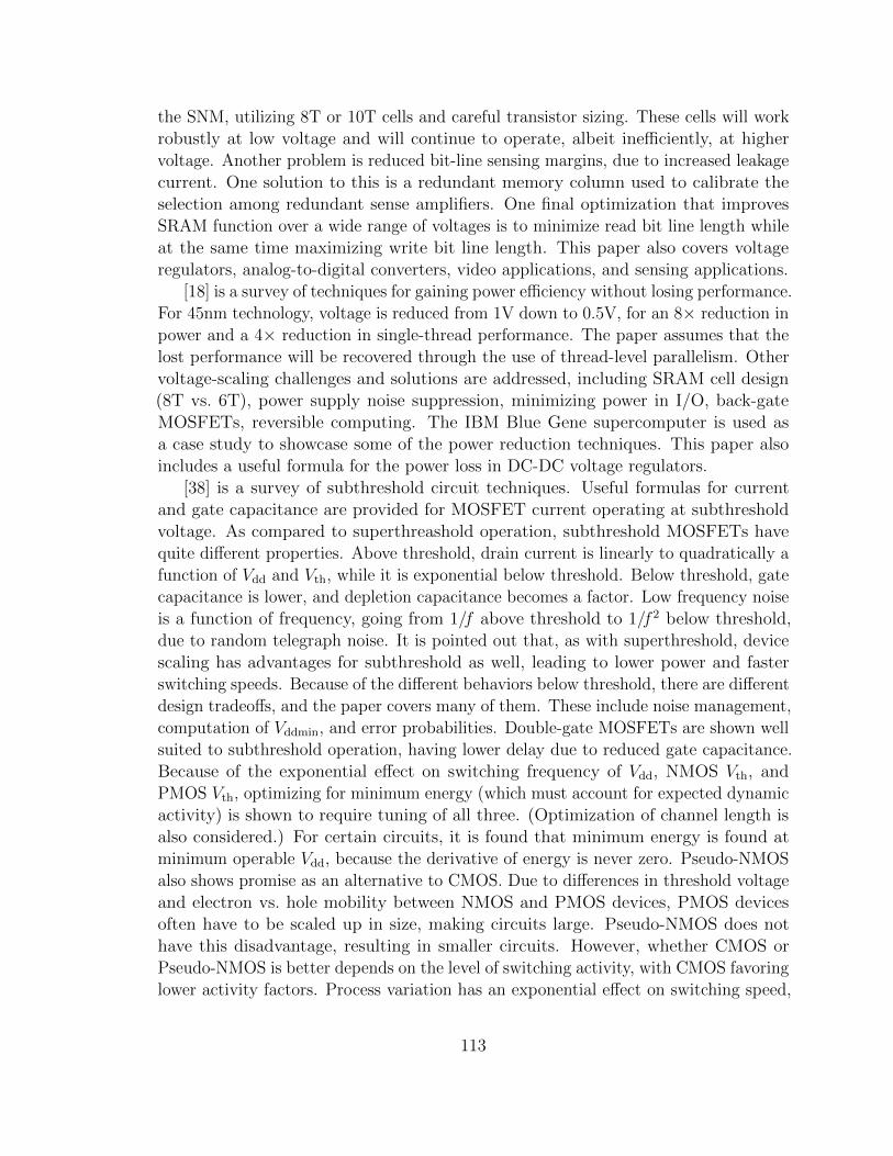
the SNM, utilizing 8T or 10T cells and careful transistor sizing. These cells will workrobustly at low voltage and will continue to operate, albeit ine�ciently, at highervoltage. Another problem is reduced bit-line sensing margins, due to increased leakagecurrent. One solution to this is a redundant memory column used to calibrate theselection among redundant sense amplifiers. One final optimization that improvesSRAM function over a wide range of voltages is to minimize read bit line length whileat the same time maximizing write bit line length. This paper also covers voltageregulators, analog-to-digital converters, video applications, and sensing applications.
[18] is a survey of techniques for gaining power e�ciency without losing performance.For 45nm technology, voltage is reduced from 1V down to 0.5V, for an 8⇥ reduction inpower and a 4⇥ reduction in single-thread performance. The paper assumes that thelost performance will be recovered through the use of thread-level parallelism. Othervoltage-scaling challenges and solutions are addressed, including SRAM cell design(8T vs. 6T), power supply noise suppression, minimizing power in I/O, back-gateMOSFETs, reversible computing. The IBM Blue Gene supercomputer is used asa case study to showcase some of the power reduction techniques. This paper alsoincludes a useful formula for the power loss in DC-DC voltage regulators.
[38] is a survey of subthreshold circuit techniques. Useful formulas for currentand gate capacitance are provided for MOSFET current operating at subthresholdvoltage. As compared to superthreashold operation, subthreshold MOSFETs havequite di↵erent properties. Above threshold, drain current is linearly to quadratically afunction of Vdd and Vth, while it is exponential below threshold. Below threshold, gatecapacitance is lower, and depletion capacitance becomes a factor. Low frequency noiseis a function of frequency, going from 1/f above threshold to 1/f 2 below threshold,due to random telegraph noise. It is pointed out that, as with superthreshold, devicescaling has advantages for subthreshold as well, leading to lower power and fasterswitching speeds. Because of the di↵erent behaviors below threshold, there are di↵erentdesign tradeo↵s, and the paper covers many of them. These include noise management,computation of Vddmin, and error probabilities. Double-gate MOSFETs are shown wellsuited to subthreshold operation, having lower delay due to reduced gate capacitance.Because of the exponential e↵ect on switching frequency of Vdd, NMOS Vth, andPMOS Vth, optimizing for minimum energy (which must account for expected dynamicactivity) is shown to require tuning of all three. (Optimization of channel length isalso considered.) For certain circuits, it is found that minimum energy is found atminimum operable Vdd, because the derivative of energy is never zero. Pseudo-NMOSalso shows promise as an alternative to CMOS. Due to di↵erences in threshold voltageand electron vs. hole mobility between NMOS and PMOS devices, PMOS devicesoften have to be scaled up in size, making circuits large. Pseudo-NMOS does nothave this disadvantage, resulting in smaller circuits. However, whether CMOS orPseudo-NMOS is better depends on the level of switching activity, with CMOS favoringlower activity factors. Process variation has an exponential e↵ect on switching speed,
113

and the e↵ect is di↵erent for NMOS and PMOS. It is shown that adaptive forward orreverse body bias can be used to rebalance rise and fall times that are thrown out ofbalance by variation. Because of the e↵ect of switching activity on optimal energy (thetradeo↵ between switching and leakage energy), various architectural principles arepresented. These include tuning degrees of pipelining and parallelism (replication ofcircuitry). Reactive (“event-driven”) power gating is also suggested. For Static RAMs,standard 6T cells are found to be completely unsuitable for subthreshold operation,and 8T cells are suggested instead. Due to the fact that SRAMs have low activityfactors and are therefore dominated by leakage power, di↵erent Vdd, Vth, and channellength optimizations are required. A di↵erential Schmitt trigger SRAM cell also ispresented as an alternative with certain advantages, such as reduced sensitivity toprocess variation. Finally, tunneling-carbon nanotube FETs are considered, and itis shown how the increased (exponential) sensitivity to factors such as temperaturemakes subthreshold devices useful as sensors.
[48] addresses circuit challenges in nanoscale circuits at below nominal voltage. Vmin
is limited by a combination of factors including maximum Vth and power supply fluc-tuations, �Vps. Vmin is di↵erent for di↵erent structures, such as logic blocks, SRAMs,and DRAMs. Various circuit techniques are introduced that aid in Vmin reduction foreach of these structures. These include transistor up-sizing and transistor and circuittechniques for reducing Vth and Vth variation. Circuit techniques suggested revolvearound using FinFETs, and RAM techniques account for error-repair redundancy.
[78] achieves significant power reduction by combining dynamic voltage scaling(DVS) with adaptive body bias (ABB). A method is presented for identifying theoptimal Vdd and Vbs for a given circuit and frequency target. [81] describes the use oftemperature and current sensors in 90nm Itaniums in order to maximize performanceunder power and temperature constraints. In [123], a linear programming method ispresented to optimize a CMP for performance under a power budget; performance ismaximized through variation-aware task scheduling and selection of core voltage andfrequency.
Various works have examined dual and multi-Vdd designs with the goal of improvingenergy e�ciency. Most have focused on tuning the delay vs. power-consumption ofpaths at fine granularity within the processor. For instance, in [65], circuit blocks alongcritical paths are assigned to the higher power supply while blocks along non-criticalpaths are assigned to a lower power supply. This converts the timing slack fromnon-critical paths to energy savings. In [106] power optimization is achieved withsimultaneous Vdd and Vth assignment. [54] presents a solution that uses a secondhigher Vdd rail for speeding up critical paths in near-threshold circuits at very fine(standard cell row) granularity. [60] and [59] are dual-vdd solutions for subthresholdcircuits. A lower voltage rail is provided that reduces timing slack on non-criticalcircuit paths, reducing power. In [72] Liang et al. proposed voltage interpolation forreducing delay variation. Their solution involves very fine-grained voltage selection,
114

at the pipeline-stage level. This requires providing each pipeline stage with two powergates. [127] also employs dual supplies but clusters low-Vdd cells together and high-Vdd
cells together, along with level-converting latches, to minimize the number of levelconverters. Calhoun and Chandrakasan proposed local voltage dithering [15] to achievevery fast dynamic voltage scaling in subthreshold chips.
[28] introduces a cache designed to reduce cache memory access energy, designedto operate e�ciently in low-voltage and high-performance modes. A subset of cacheways are made of larger SRAM cells, allowing them to be accessed reliabily at NTvoltages, with the remaining ways made of standard SRAM cells. In high-performancemode, the cache is operated at nominal voltage and accessed in a unified manner. Inlow-voltage mode, the NT (filter) ways are accessed first. If there is a miss, then therest of the cache is accessed on a subsequent cycle. If there is a hit, then the cacheline that is hit is swapped with the one in the filter portion.
115

CHAPTER 8
Conclusions
In this work, we have addressed several challenges facing modern semiconduc-tor technologies. A flexible “FIT-targeting” solution has been presented to protectagainst logic faults, allowing the level of error protection to be tuned dynamicallyto system and application criticality, environment, and runtime behavior. Parichutepresents a solution to high bit failure rates in static RAM devices at ultra-low voltage.And Steamroller implements simple dual-voltage and clock divider techniques toreduce power and performance ine�ciencies caused by the increasing e↵ects of processvariation, particularly at low voltage. Booster address frequency heterogeneity inmany-core processors at low voltage by interpolating between two sets of optimalvoltage and frequency states. Additionally, Booster addresses the interaction betweenprocess variation, many-core processors, and parallel scientific workloads. We examineine�ciencies due to imbalance in workloads, redistributing power to cores that needit, away from those that are idle. And finally, VRSync addresses the impact on powerdelivery of synchronized parallel workloads in many-core processors, completely elimi-nating voltage emergencies using a purely reactive technique based on synchronizationprimitives and other explicit events.
116

APPENDIX A
Delay and Power Models
For power and delay models at near threshold, we use the models from Markovicet al. [77], reproduced here in Equations A.1, A.2, A.3, A.4 and A.5.
Ids is the drain-source current used to compute dynamic power. ILeakage is theleakage current used to compute static power. IC is a parameter called the inversioncoe�cient that describes proximity to threshold voltage, ⌘ is the subthreshold slope,µ is the carrier mobility, and kfit and ktp are fitting parameters for current and delay.
Ids =Is · ICkfit
(A.1)
Is = 2 ·µ ·Cox ·W
L·�2
t · ⌘ (A.2)
IC =
✓ln
✓e
(1+�) ·Vdd�Vth2 · ⌘ ·�t + 1
◆◆2
(A.3)
tp =ktp ·CLoad ·Vdd
2 · ⌘ ·µ ·Cox · WL·�2
t
.kfitIC
(A.4)
ILeakage = Is · e� ·Vdd�Vth
⌘ ·�t (A.5)
117

BIBLIOGRAPHY
[1] A. Agarwal, B. Paul, S. Mukhopadhyay, and K. Roy. Process variation inembedded memories: failure analysis and variation aware architecture. IEEEJournal of Solid-State Circuits, 40(9):1804–1814, September 2005.
[2] N. Aggarwal, P. Ranganathan, N. P. Jouppi, and J. E. Smith. Configurable iso-lation: building high availability systems with commodity multi-core processors.SIGARCH Comput. Archit. News, 35(2):470–481, 2007.
[3] R. S. Amant, D. A. Jimenez, and D. Burger. Low-power, high-performance analogneural branch prediction. In International Symposium on Microarchitecture,pages 447–458, Los Alamitos, CA, USA, 2008. IEEE Computer Society.
[4] H. Ando, K. Seki, S. Sakashita, M. Aihara, Kan, and K. Imada. Acceleratedtesting of a 90nm SPARC64 V microprocessor for neutron SER. IEEE Workshopon Silicon Errors in Logic - System E↵ects (SELSE), 2007.
[5] T. M. Austin. Diva: a reliable substrate for deep submicron microarchitecturedesign. In International Symposium on Microarchitecture, pages 196–207. IEEEComputer Society, 1999.
[6] O. Azizi, A. Mahesri, B. C. Lee, S. J. Patel, and M. Horowitz. Energy-performance tradeo↵s in processor architecture and circuit design: a marginalcost analysis. SIGARCH Comput. Archit. News, 38:26–36, June 2010.
[7] C. Berrou, A. Glavieux, and P. Thitimajshima. Near shannon limit error-correcting coding and decoding: Turbo-codes. 1. Communications, 1993. ICC 93.Geneva. Technical Program, Conference Record, IEEE International Conferenceon, 2:1064–1070 vol.2, 1993.
[8] A. Bhattacharjee and M. Martonosi. Thread criticality predictors for dynamicperformance, power, and resource management in chip multiprocessors. InInternational Symposium on Computer Architecture, pages 290–301. ACM, 2009.
118

[9] A. Biswas, N. Soundararajan, S. S. Mukherjee, and S. Gurumurthi. QuantizedAVF: A means of capturing vulnerability variations over small windows oftime. In IEEE Workshop on Silicon Errors in Logic - System E↵ects. StanfordUniversity, March 2009.
[10] R. D. Blumofe and C. E. Leiserson. Scheduling multithreaded computations bywork stealing. Journal of the ACM, 46:720–748, September 1999.
[11] S. Borkar, T. Karnik, S. Narendra, J. Tschanz, A. Keshavarzi, and V. De.Parameter variations and impact on circuits and microarchitecture. In DesignAutomation Conference, June 2003.
[12] D. Brooks, V. Tiwari, and M. Martonosi. Wattch: A framework for architectural-level power analysis and optimizations. In International Symposium on ComputerArchitecture, June 2000.
[13] D. Burnett, J. Higman, A. Hoefler, B. Li, and P. Kuhn. Variation in naturalthreshold voltage of NVM circuits due to dopant fluctuations and its impact onreliability. In International Electron Devices Meeting, pages 529–534, 2002.
[14] Q. Cai, J. Gonzalez, R. Rakvic, G. Magklis, P. Chaparro, and A. Gonzalez.Meeting points: Using thread criticality to adapt multicore hardware to parallelregions. In International Conference on Parallel Architectures and CompilationTechniques, pages 240–249, October 2008.
[15] B. Calhoun and A. Chandrakasan. Ultra-dynamic voltage scaling (UDVS) usingsub-threshold operation and local voltage dithering. 41(1):238–245, January2006.
[16] B. Calhoun and A. Chandrakasan. A 256-kb 65-nm sub-threshold SRAMdesign for ultra-low-voltage operation. IEEE Journal of Solid-State Circuits,42(3):680–688, 2007.
[17] A. Chandrakasan, D. Daly, D. Finchelstein, J. Kwong, Y. Ramadass, M. Sinangil,V. Sze, and N. Verma. Technologies for ultradynamic voltage scaling. Proceedingsof the IEEE, 98(2):191 –214, February 2010.
[18] L. Chang, D. Frank, R. Montoye, S. Koester, B. Ji, P. Coteus, R. Dennard,and W. Haensch. Practical strategies for power-e�cient computing technologies.Proceedings of the IEEE, 98(2):215 –236, feb. 2010.
[19] G. K. Chen, D. Blaauw, T. Mudge, D. Sylvester, and N. S. Kim. Yield-drivennear-threshold SRAM design. In International Conference on Computer-aidedDesign, pages 660–666. IEEE Press, 2007.
119

[20] Z. Chishti, A. R. Alameldeen, C. Wilkerson, W. Wu, and S.-L. Lu. Improvingcache lifetime reliability at ultra-low voltages. In International Symposium onMicroarchitecture, 2009.
[21] K. Constantinides, O. Mutlu, and T. Austin. Online design bug detection: Rtlanalysis, flexible mechanisms, and evaluation. In International Symposium onMicroarchitecture, pages 282–293, November 2008.
[22] T. Dell. A white paper on the benefits of chipkill-correct ECC for PC servermain memory. IBM Microelectronics Division Whitepaper, 1997.
[23] D. Donoho. Compressed sensing. Information Theory, IEEE Transactions on,52(4):1289–1306, 2006.
[24] J. Dorsey, S. Searles, M. Ciraula, S. Johnson, N. Bujanos, D. Wu, M. Braganza,S. Meyers, E. Fang, and R. Kumar. An integrated quad-core Opteron processor.In International Solid-State Circuits Conference, pages 102–103, February 2007.
[25] R. Dreslinkski, B. Zhai, T. Mudge, D. Blaauw, and D. Sylvester. An energye�cient parallel architecture using near threshold operation. In Proceedingsof the 16th International Conference on Parallel Architecture and CompilationTechniques, pages 175–188. IEEE Computer Society, 2007.
[26] R. Dreslinski. Near Threshold Computing: From Single Core to Many-CoreEnergy E�cient Architectures. PhD thesis, The University of Michigan, 2011.
[27] R. Dreslinski, M. Wieckowski, D. Blaauw, D. Sylvester, and T. Mudge. Near-threshold computing: Reclaiming Moore’s law through energy e�cient integratedcircuits. Proceedings of the IEEE, 98(2):253 –266, feb. 2010.
[28] R. G. Dreslinski, G. K. Chen, T. Mudge, D. Blaauw, D. Sylvester, and K. Flaut-ner. Reconfigurable energy e�cient near threshold cache architectures. InInternational Symposium on Microarchitecture, pages 459–470. IEEE ComputerSociety, 2008.
[29] A. Duran, J. Corbalan, and E. Ayguade. Evaluation of OpenMP task schedulingstrategies. In International Conference on OpenMP in a New Era of Parallelism,pages 100–110, May 2008.
[30] P. Elias. Error-free coding. IRE Professional Group on Information Theory,4(4):29–37, 1954.
[31] D. Ernst, N. S. Kim, S. Das, S. Pant, R. Rao, T. Pham, C. Ziesler, D. Blaauw,T. Austin, K. Flautner, and T. Mudge. Razor: A low-power pipeline based oncircuit-level timing speculation. In International Symposium on Microarchitec-ture, pages 7–18, December 2003.
120

[32] Y. Guo, R. Barik, R. Raman, and V. Sarka. Work-first and help-first schedulingpolicies for async-finish task parallelism. In IEEE International Parallel andDirstirbuted Processing Symposium, pages 1–12, May 2009.
[33] M. Gupta, J. Oatley, R. Joseph, G.-Y. Wei, and D. Brooks. Understandingvoltage variations in chip multiprocessors using a distributed power-deliverynetwork. In Design Automation and Test in Europe, pages 1–6, April 2007.
[34] M. S. Gupta, K. K. Rangan, M. D. Smith, G.-Y. Wei, and D. Brooks. Towards asoftware approach to mitigate voltage emergencies. In International Symposiumon Low Power Electronics and Design, pages 123–128, August 2007.
[35] M. S. Gupta, K. K. Rangan, M. D. Smith, G.-Y. Wei, and D. Brooks. Decor:A delayed commit and rollback mechanism for handling inductive noise inprocessors. In IEEE International Symposium on High-Performance ComputerArchitecture, pages 381–392, February 2008.
[36] M. S. Gupta, V. Reddi, G. Holloway, G.-Y. Wei, and D. Brooks. An event-guidedapproach to reducing voltage noise in processors. In Design Automation andTest in Europe, pages 160–165, April 2009.
[37] S. Gupta, S. Feng, A. Ansari, J. Blome, and S. Mahlke. The stagenet fabricfor constructing resilient multicore systems. In International Symposium onMicroarchitecture, pages 141–151. IEEE Computer Society, 2008.
[38] S. Gupta, A. Raychowdhury, and K. Roy. Digital computation in subthresholdregion for ultralow-power operation: A device-circuit-architecture codesignperspective. Proceedings of the IEEE, 98(2):160 –190, feb. 2010.
[39] P. Hazucha, T. Karnik, J. Maiz, S. Walstra, B. Bloechel, J. Tschanz, G. Dermer,S. Hareland, P. Armstrong, and S. Borkar. Neutron soft error rate measurementsin a 90-nm cmos process and scaling trends in sram from 0.25-µm to 90-nmgeneration. In Electron Devices Meeting, 2003. IEDM ’03 Technical Digest.IEEE International, pages 21.5.1–21.5.4, Dec. 2003.
[40] Y. He and P. Ching. Performance evaluation of adaptive two-dimensional turboproduct codes composed of hamming codes. In International Conference onIntegration Technology, pages 103–107, March 2007.
[41] S. Herbert and D. Marculescu. Mitigating the impact of variability on chip-multiprocessor power and performance. IEEE Transactions on Very Large ScaleIntegrated Systems, 17:1520–1533, October 2009.
[42] H. Y. Hsiao, D. Bossen, and R. Chien. Orthogonal latin square codes. IBMJournal of Research and Development, 14(4):390–394, July 1970.
121

[43] E. Humenay, D. Tarjan, and K. Skadron. Impact of process variations onmulticore performance symmetry. In Design, Automation and Test in Europe,April 2007.
[44] I. C. i7 Processor. http://www.intel.com/products/processor/corei7.
[45] Intel 64 and IA-32 Architectures Software Developer’s Manual, Volume 3, Section14.7 (as of November 2011).
[46] Voltage regulator module (VRM) and enterprise voltage regulator-down (EVRD)11.1 design guidelines. Technical report, Intel Corp., September 2009.
[47] E. Ipek, O. Mutlu, J. F. Martınez, and R. Caruana. Self-optimizing memorycontrollers: A reinforcement learning approach. In International Symposium onComputer Architecture, pages 39–50. IEEE Computer Society, 2008.
[48] K. Itoh. Adaptive circuits for the 0.5-V nanoscale CMOS era. In InternationalSolid-State Circuits Conference, pages 14–20, February 2009.
[49] International Technology Roadmap for Semiconductors (2009).
[50] N. James, P. Restle, J. Friedrich, B. Huott, and B. McCredie. Comparisonof split-versus connected-core supplies in the POWER6 microprocessor. InInternational Solid-State Circuits Conference, pages 298–604, February 2007.
[51] H. Jiang and M. Marek-Sadowska. Power gating scheduling for power/groundnoise reduction. In Design Automation Conference, pages 980–985, New York,NY, USA, 2008. ACM.
[52] R. Joseph, D. Brooks, and M. Martonosi. Control techniques to eliminate voltageemergencies in high performance processors. In IEEE International Symposiumon High-Performance Computer Architecture, pages 79–90, 2003.
[53] A. B. Kahng, B. Li, L.-S. Peh, and K. Samadi. ORION 2.0: A fast and accurateNoC power and area model for early-stage design space exploration. In DesignAutomation and Test in Europe, pages 423–428, 2009.
[54] M. R. Kakoee, A. Sathanur, A. Pullini, J. Huisken, and L. Benini. Automaticsynthesis of near-threshold circuits with fine-grained performance tunability.In Proceedings of the 16th ACM/IEEE international symposium on Low powerelectronics and design, ISLPED ’10, pages 401–406, New York, NY, USA, 2010.ACM.
[55] C. Kim, K. Roy, S. Hsu, R. Krishnamurthy, and S. Borkar. An on-die cmosleakage current sensor for measuring process variation in sub-90nm genera-tions. In Integrated Circuit Design and Technology, 2005. ICICDT 2005. 2005International Conference on, pages 221 – 222, May 2005.
122

[56] C. Kim, K. Roy, S. Hsu, R. Krishnamurthy, and S. Borkar. A process variationcompensating technique with an on-die leakage current sensor for nanometerscale dynamic circuits. Very Large Scale Integration (VLSI) Systems, IEEETransactions on, 14(6):646 –649, 2006.
[57] H.-i. Kim and K. Roy. Ultra-low power dlms adaptive filter for hearing aidapplications. In International Symposium on Low Power Electronics and Design,pages 352–357. ACM, 2001.
[58] J. Kim, N. Hardavellas, K. Mai, B. Falsafi, and J. Hoe. Multi-bit error tolerantcaches using two-dimensional error coding. In International Symposium onMicroarchitecture, pages 197–209. IEEE Computer Society, 2007.
[59] K. Kim and V. Agrawal. Minimum Energy CMOS Design with Dual SubthresholdSupply and Multiple Logic-Level Gates. In Proc. 12th International Symposiumon Quality Electronic Design, 2011.
[60] K. Kim and V. D. Agrawal. True minimum energy design using dual below-threshold supply voltages. VLSI Design, International Conference on, 0:292–297,2011.
[61] W. Kim, D. Brooks, and G.-Y. Wei. A fully-integrated 3-level DC/DC converterfor nanosecond-scale DVS with fast shunt regulation. In International Solid-StateCircuits Conference, pages 268–270, February 2011.
[62] W. Kim, M. Gupta, G.-Y. Wei, and D. Brooks. System level analysis of fast, per-core DVFS using on-chip switching regulators. In IEEE International Symposiumon High-Performance Computer Architecture, February 2008.
[63] P. Koopman and T. Chakravarty. Cyclic redundancy code (CRC) polynomialselection for embedded networks. In Dependable Systems and Networks, 2004International Conference on, pages 145–154.
[64] F. Koushanfar, P. Boufounos, and D. Shamsi. Post-silicon timing characterizationby compressed sensing. In Proceedings of the 2008 IEEE/ACM InternationalConference on Computer-Aided Design, pages 185–189. IEEE Press, 2008.
[65] S. Kulkarni, A. Srivastava, and D. Sylvester. A new algorithm for improvedVDD assignment in low power dual VDD systems. In International Symposiumon Low Power Electronics and Design, pages 200–205, May 2004.
[66] N. Kurd, P. Mosalikanti, M. Neidengard, J. Douglas, and R. Kumar. Nextgeneration Intel Core micro-architecture (Nehalem) clocking. IEEE Journal ofSolid-State Circuits, 44(4):1121–1129, April 2009.
123

[67] C.-Y. Lee, R. Uzsoy, and L. A. Martin-Vega. E�cient algorithms for schedulingsemiconductor burn-in operations. Operations Research, 40(4):pp. 764–775, 1992.
[68] J. Leverich, M. Monchiero, V. Talwar, P. Ranganathan, and C. Kozyrakis. Powermanagement of datacenter workloads using per-core power gating. 8:48–51, July2009.
[69] J. Li, J. Martınez, and M. C. Huang. The thrifty barrier: Energy-awaresynchronization in shared-memory multiprocessors. In IEEE InternationalSymposium on High-Performance Computer Architecture, pages 14–24. IEEEComputer Society, 2004.
[70] X. Li, S. Adve, P. Bose, and J. Rivers. Softarch: an architecture-level tool formodeling and analyzing soft errors. In Dependable Systems and Networks, 2005.DSN 2005. Proceedings. International Conference on, pages 496–505, 2005.
[71] X. Liang and D. Brooks. Mitigating the impact of process variations on processorregister files and execution units. In International Symposium on Microarchitec-ture, pages 504–514. IEEE Computer Society, December 2006.
[72] X. Liang, G.-Y. Wei, and D. Brooks. Revival: A variation-tolerant architectureusing voltage interpolation and variable latency. IEEE Micro, 29(1):127–138,2009.
[73] C. Liu, A. Sivasubramaniam, M. Kandemir, and M. J. Irwin. Exploiting barriersto optimize power consumption of CMPs. In IEEE International Parallel andDirstirbuted Processing Symposium, pages 1–5, April 2005.
[74] Linear Technologies, LTC3729L. http://www.linear.com/product/
LTC3729L-6.
[75] Linear technologies, LTSpice. http://www.linear.com/designtools/
software/LTspice.
[76] D. Marculescu and E. Talpes. Variability and energy awareness: Amicroarchitecture-level perspective. In Design Automation Conference, June2005.
[77] D. Markovic, C. Wang, L. Alarcon, T.-T. Liu, and J. Rabaey. Ultralow-powerdesign in near-threshold region. Proceedings of the IEEE, 98(2):237 –252, feb.2010.
[78] S. Martin, K. Flautner, T. Mudge, and D. Blaauw. Combined dynamic voltagescaling and adaptive body biasing for lower power microprocessors under dynamicworkloads. In International Conference on Computer-aided Design, pages 721–725, 2002.
124

[79] P. Maulik and D. Mercer. A DLL-based programmable clock multiplier in 0.18-um CMOS with -70 dBc reference spur. IEEE Journal of Solid-State Circuits,42(8):1642–1648, August 2007.
[80] R. McGowen, C. Poirier, C. Bostak, J. Ignowski, M. Millican, W. Parks, andS. Na↵ziger. Power and temperature control on a 90-nm Itanium family processor.IEEE Journal of Solid-State Circuits, 41(1):229–237, January 2006.
[81] R. McGowen, C. A. Poirier, C. Bostak, J. Ignowski, M. Millican, W. H. Parks,and S. Na↵ziger. Power and temperature control on a 90-nm Itanium familyprocessor. Journal of Solid-State Circuits, January 2006.
[82] R. McGowen, C. A. Poirier, C. Bostak, J. Ignowski, M. Millican, W. H. Parks,and S. Na↵ziger. Power and temperature control on a 90-nm Itanium familyprocessor. IEEE Journal of Solid-State Circuits, 41(1):229–237, January 2006.
[83] J. Mellor-Crummey and M. Scott. Algorithms for scalable synchronizationon shared-memory multiprocessors. ACM Transactions on Computer Systems(TOCS), 9(1):21–65, 1991.
[84] T. Miller, J. Dinan, R. Thomas, B. Adcock, and R. Teodorescu. Parichute:Generalized turbocode-based error correction for near-threshold caches. InInternational Symposium on Microarchitecture (MICRO), 2010.
[85] T. Miller, R. Thomas, X. Pan, N. Sedaghati, and R. Teodorescu. Booster:Reactive core acceleration for mitigating the e↵ects of process variation andapplication imbalance in low-voltage chips. In IEEE International Symposiumon High-Performance Computer Architecture, pages 27–38, February 2012.
[86] T. Miller, R. Thomas, and R. Teodorescu. Mitigating the e↵ects of processvariation in ultra-low voltage chip multiprocessors using dual supply voltagesand half-speed stages. 11(1), 2012.
[87] T. Miller and P. Urkedal. http://opengraphics.org.
[88] J. Mitchell, D. Henderson, and G. Ahrens. IBM POWER5 processor-basedservers: A highly available design for business-critical applications. IBM Techni-cal Report, 2006.
[89] S. Mitra, M. Zhang, N. Seifert, B. Gill, S. Waqas, and K. S. Kim. Combinationallogic soft error correction. In International Test Conference, November 2006.
[90] T. K. Moon. Error Correction Coding: Mathematical Methods and Algorithms.Wiley-Interscience, 2005.
125

[91] S. S. Mukherjee, C. Weaver, J. Emer, S. K. Reinhardt, and T. Austin. Asystematic methodology to compute the architectural vulnerability factors for ahigh-performance microprocessor. In International Symposium on Microarchi-tecture, page 29, Washington, DC, USA, 2003. IEEE Computer Society.
[92] S. Mukhopadhyay, H. Mahmoodi, and K. Roy. Statistical design and optimizationof SRAM cell for yield enhancement. In International Conference on Computer-aided Design, pages 10–13, Washington, DC, USA, 2004.
[93] N. Muralimanohar, R. Balasubramonian, and N. P. Jouppi. CACTI 6.0: A toolto model large caches. Technical Report HPL-2009-85, HP Labs, 2009.
[94] Nangate open cell library. http://www.nangate.com/.
[95] E. Normand. Single event upset at ground level. IEEE Transactions on NuclearScience, 43(6):2742–2750, 1996.
[96] M. D. Powell and T. N. Vijaykumar. Pipeline mu✏ing and a priori currentramping: architectural techniques to reduce high-frequency inductive noise. InInternational Symposium on Low Power Electronics and Design, pages 223–228,August 2003.
[97] R. Pyndiah. Near-optimum decoding of product codes: Block turbo codes. IEEETransactions on Communications, 46(8):1003–1010, 1998.
[98] N. Quach. High availability and reliability in the itanium processor. IEEEMicro, 20(5):61–69, 2000.
[99] R Development Core Team. R: A Language and Environment for StatisticalComputing. R Foundation for Statistical Computing, 2006. http://www.R-project.org.
[100] K. K. Rangan, G.-Y. Wei, and D. Brooks. Thread motion: Fine-grained powermanagement for multi-core systems. In International Symposium on ComputerArchitecture, pages 302–313, June 2009.
[101] V. J. Reddi, M. S. Gupta, G. Holloway, G. yeon Wei, M. D. Smith, and D. Brooks.Voltage emergency prediction: Using signatures to reduce operating margins. InIEEE International Symposium on High-Performance Computer Architecture,2009.
[102] V. J. Reddi, S. Kanev, W. Kim, S. Campanoni, M. D. Smith, G.-Y. Wei, andD. Brooks. Voltage smoothing: Characterizing and mitigating voltage noise inproduction processors via software-guided thread scheduling. In InternationalSymposium on Microarchitecture, pages 77–88. IEEE Computer Society, 2010.
126

[103] J. Renau, B. Fraguela, J. Tuck, W. Liu, M. Prvulovic, L. Ceze, K. Strauss,S. Sarangi, P. Sack, and P. Montesinos. SESC Simulator, January 2005.http://sesc.sourceforge.net.
[104] P. Ribeiro Jr. and P. Diggle. geoR: A package for geostatistical analysis. R-NEWS, 1(2), 2001.
[105] B. F. Romanescu and D. J. Sorin. Core cannibalization architecture: improvinglifetime chip performance for multicore processors in the presence of hard faults.In PACT ’08: Proceedings of the 17th international conference on Parallelarchitectures and compilation techniques, pages 43–51, New York, NY, USA,2008. ACM.
[106] K. Roy, L. Wei, and Z. Chen. Multiple-Vdd multiple-Vth CMOS (MVCMOS)for low power applications. In IEEE International Symposium on Circuits andSystems, volume 1, pages 366–370, 1999.
[107] T. Saeki, M. Mitsuishi, H. Iwaki, and M. Tagishi. A 1.3-cycle lock time, non-PLL/DLL clock multiplier based on direct clock cycle interpolation for clockon demand. IEEE Journal of Solid-State Circuits, 35(11):1581–1590, November2000.
[108] T. Sakurai and R. Newton. Alpha-power law MOSFET model and its applicationsto CMOS inverter delay and other formulas. Journal of Solid-State Circuits,April 1990.
[109] S. Sarangi, B. Greskamp, A. Tiwari, and J. Torrellas. Eval: Utilizing pro-cessors with variation-induced timing errors. In International Symposium onMicroarchitecture, pages 423–434, November 2008.
[110] S. R. Sarangi, B. Greskamp, R. Teodorescu, J. Nakano, A. Tiwari, and J. Tor-rellas. VARIUS: A model of parameter variation and resulting timing errors formicroarchitects. IEEE Transactions on Semiconductor Manufacturing, February2008.
[111] L. Seiler, D. Carmean, E. Sprangle, T. Forsyth, M. Abrash, P. Dubey, S. Junkins,A. Lake, J. Sugerman, R. Cavin, R. Espasa, E. Grochowski, T. Juan, andP. Hanrahan. Larrabee: a many-core x86 architecture for visual computing.ACM Trans. Graph., 27(3):1–15, 2008.
[112] D. Shelepov, J. C. S. Alcaide, S. Je↵ery, A. Fedorova, N. Perez, Z. F. Huang,S. Blagodurov, and V. Kumar. Hass: a scheduler for heterogeneous multicoresystems. SIGOPS Operating Systems Review, 43(2):66–75, 2009.
127

[113] P. Shivakumar, M. Kistler, S. Keckler, D. Burger, and L. Alvisi. Modeling thee↵ect of technology trends on the soft error rate of combinational logic. InDependable Systems and Networks, 2002. DSN 2002. Proceedings. InternationalConference on, pages 389–398, 2002.
[114] P. Shivakumar, M. Kistler, S. W. Keckler, D. Burger, and L. Alvisi. Modeling thee↵ect of technology trends on the soft error rate of combinational logic. In DSN’02: Proceedings of the 2002 International Conference on Dependable Systemsand Networks, pages 389–398, Washington, DC, USA, 2002. IEEE ComputerSociety.
[115] K. Skadron, M. R. Stan, W. Huang, S. Velusamy, K. Sankaranarayanan, andD. Tarjan. Temperature-aware microarchitecture. In International Symposiumon Computer Architecture, June 2003.
[116] T. Slegel, I. Averill, R.M., M. Check, B. Giamei, B. Krumm, C. Krygowski, W. Li,J. Liptay, J. MacDougall, T. McPherson, J. Navarro, E. Schwarz, K. Shum, andC. Webb. IBM’s S/390 G5 microprocessor design. Micro, IEEE, 19(2):12–23,Mar/Apr 1999.
[117] L. Spainhower and T. A. Gregg. IBM S/390 parallel enterprise server G5 faulttolerance: a historical perspective. IBM Journal of Research and Development,43(5):863–873, 1999.
[118] H. Sun, N. Zheng, and T. Zhang. Realization of l2 cache defect tolerance usingmulti-bit ecc. In Defect and Fault Tolerance of VLSI Systems, pages 254–262,October 2008.
[119] Synopsys. Synopsys design compiler. http://synopsys.com.
[120] Synopsys formality. http://synopsys.com/Tools/Verification/
FormalEquivalence/Pages/Formality.aspx.
[121] R. Teodorescu, B. Greskamp, J. Nakano, S. R. Sarangi, A. Tiwari, and J. Tor-rellas. VARIUS: A model of parameter variation and resulting timing errors formicroarchitects. In Workshop on Architectural Support for Gigascale Integration,June 2007.
[122] R. Teodorescu, J. Nakano, A. Tiwari, and J. Torrellas. Mitigating parametervariation with dynamic fine-grain body biasing. In International Symposium onMicroarchitecture, pages 27–39, December 2007.
[123] R. Teodorescu and J. Torrellas. Variation-aware application scheduling andpower management for chip multiprocessors. In International Symposium onComputer Architecture, pages 363–374, Washington, DC, USA, 2008. IEEEComputer Society.
128

[124] A. Tiwari, S. R. Sarangi, and J. Torrellas. ReCycle: Pipeline adaptation totolerate process variation. In International Symposium on Computer Architecture,June 2007.
[125] J. Torrellas. Architectures for extreme-scale computing. IEEE Computer,42:28–35, November 2009.
[126] J. Tschanz, J. Kao, S. Narendra, R. Nair, D. Antoniadis, A. Chandrakasan,and V. De. Adaptive body bias for reducing impacts of die-to-die and within-die parameter variations on microprocessor frequency and leakage. Journal ofSolid-State Circuits, 37(11):1396–1402, February 2002.
[127] K. Usami and M. Horowitz. Clustered voltage scaling technique for low-powerdesign. In International Symposium on Low Power Electronics and Design,pages 3–8. ACM, 1995.
[128] S. R. Vangal, J. Howard, G. Ruhl, S. Dighe, H. Wilson, J. Tschanz, D. Finan,A. Singh, T. Jacob, S. Jain, V. Erraguntla, C. Roberts, Y. Hoskote, N. Borkar,and S. Borkar. An 80-tile sub-100-W TeraFLOPS processor in 65-nm CMOS.IEEE Journal of Solid-State Circuits, 43(1):29–41, january 2008.
[129] K. R. Walcott, G. Humphreys, and S. Gurumurthi. Dynamic prediction of archi-tectural vulnerability from microarchitectural state. In International Symposiumon Computer Architecture, San Diego, California, USA, June 2007.
[130] C. Weaver and T. Austin. A fault tolerant approach to microprocessor design.In DSN, July 2001.
[131] C. Wilkerson, A. R. Alameldeen, Z. Chishti, W. Wu, D. Somasekhar, and S.-L.Lu. Reducing cache power with low-cost, multi-bit error-correcting codes. InInternational Symposium on Computer Architecture, 2010.
[132] C. Wilkerson, H. Gao, A. R. Alameldeen, Z. Chishti, M. Khellah, and S.-L.Lu. Trading o↵ cache capacity for reliability to enable low voltage operation.In International Symposium on Computer Architecture, pages 203–214. IEEEComputer Society, 2008.
[133] P.-C. Yew, N.-F. Tzeng, and D. Lawrie. Distributing hot-spot addressing inlarge-scale multiprocessors. IEEE Transactions on Computers, C-36(4):388–395,April 1987.
[134] D. Yoon and M. Erez. Memory mapped ECC: Low-cost error protection forlast level caches. ACM SIGARCH Computer Architecture News, 37(3):116–127,2009.
129

[135] B. Zhai, D. Blaauw, D. Sylvester, and S. Hanson. A sub-200mV 6T SRAM in0.13µm CMOS. In International Solid-State Circuits Conference, 2007.
[136] B. Zhai, R. G. Dreslinski, D. Blaauw, T. Mudge, and D. Sylvester. Energye�cient near-threshold chip multi-processing. In International Symposium onLow Power Electronics and Design, pages 32–37. ACM, 2007.
[137] W. Zhao and Y. Cao. New generation of predictive technology model for sub-45nm design exploration. In ISQED ’06: Proceedings of the 7th InternationalSymposium on Quality Electronic Design, pages 585–590, Washington, DC, USA,2006. IEEE Computer Society.
[138] P. Zhou, B. Zhao, J. Yang, and Y. Zhang. A durable and energy e�cient mainmemory using phase change memory technology. In International Symposiumon Computer Architecture, pages 14–23, New York, NY, USA, 2009. ACM.
130