Embed Size (px)
Citation preview

Copyright ANPEC Electronics Corp.Rev. A.10 - Aug., 2009
APW7063
www.anpec.com.tw1
ANPEC reserves the right to make changes to improve reliability or manufacturability without notice, and advisecustomers to obtain the latest version of relevant information to verify before placing orders.
Synchronous Buck PWM and Linear Controller
• Provide Two Regulated Voltages
- Synchronous Rectified Buck PWM Controller
- Linear Controller
• Fast Transient Response
- 0~85% Duty Ratio
• Excellent Output Voltage Regulation
- 0.8V Internal Reference
- ±1% Over Line Voltage and Temperature
• Over Current Protection
- Sense Low-Side MOSFET’s RDS(ON)
• Under Voltage Lockout
• Small Converter Size
- 250kHz Free-Running Oscillator
- Programmable From 70kHz to 800kHz
• 14-Lead SOIC Package
• Lead Free and Green Devices Available
(RoHS Compliant)
Features General Description
The APW7063 integrates PWM and linear controller, aswell as the monitoring and protection functions into asingle package. The synchronous PWM controller whichdrives dual N-channel MOSFETs, which provides onecontrolled power outputs with under-voltage and over-current protections. Linear controller drives an externalN-channel MOSFET with under-voltage protection.APW7063 provides excellent regulation for output loadvariation. An internal 0.8V temperature-compensated ref-erence voltage is designed to meet the various low out-put voltage applications. APW7063 includes a 250kHzfree-running triangle-wave oscillator that is adjustablefrom 70kHz to 800kHz.A power-on-reset (POR) circuit limits the VCC minimumopearting supply voltage to assure the controller workingwell. Over current protection is achieved by monitoringthe voltage drop across the low side MOSFET, eliminat-ing the need for a current sensing resistor and short cir-cuit condition is detected through the FB pin. The over-current protection triggers the soft-start function until thefault events be removed, but Under-voltage protection willshutdown IC directly.Pull the COMP pin below 0.4V will shutdown the controller,and both gate drive signals will be low.
Applications
• Graphic Cards
• Memory Power Supplies
• DSL or Cable MODEMs
• Set Top Boxes
• Low-Voltage Distributed Power Supplies
Pin Configuration
1
2
3
4
5
6
7
10
9
8
11
12
13
14RT
VREG
SS
FB
COMP
FBL
GND
VCC
DRIVE
LGATE
PGND
BOOT
UGATEPHASE
SOP-14(Top View)

Copyright ANPEC Electronics Corp.Rev. A.10 - Aug., 2009
APW7063
www.anpec.com.tw2
Ordering and Marking Information
Note: ANPEC lead-free products contain molding compounds/die attach materials and 100% matte tin plate termination finish; whichare fully compliant with RoHS. ANPEC lead-free products meet or exceed the lead-free requirements of IPC/JEDEC J-STD-020D forMSL classification at lead-free peak reflow temperature. ANPEC defines “Green” to mean lead-free (RoHS compliant) and halogenfree (Br or Cl does not exceed 900ppm by weight in homogeneous material and total of Br and Cl does not exceed 1500ppm byweight).
Symbol Parameter Rating Unit
VCC VCC to GND 30 V
LGATE LGATE to GND 30 V
DRIVE DRIVE to GND 30 V
UGATE UGATE to GND 30 V
VBOOT BOOT to GND 30 V
PHASE to GND 30 V
Operating Junction Temperature 0~150 oC
TSTG Storage Temperature -65 ~ 150 oC
TSDR Maximum Lead Soldering Temperature, 10 Seconds 260 oC
Range Symbol Parameter
Min. Typ. Max. Unit
VCC Supply Voltage 8 12 19 V
VBOOT Boot Voltage - - 26 V
Absolute Maximum Ratings (Note 1)
Recommended Operating Conditions
Note 1: Absolute Maximum Ratings are those values beyond which the life of a device may be impaired. Exposure to absolutemaximum rating conditions for extended periods may affect device reliability.
Symbol Parameter Typical Value Unit
θJA Junction to Ambient Resistance in Free Air (Note 2)
SOP-14 160 oC/W
Thermal Characteristics
APW7063
Handling Code
Package Code
APW7063 K : APW7063XXXXX XXXXX - Date Code
Assembly Material
Temperature Range
Package Code K : SOP-14Operating Ambient Temperature Range C : 0 to 70 oCHandling Code TR : Tape & ReelAssembly Material G : Halogen and Lead Free Device
Note 2: θJA is measured with the component mounted on a high effective thermal conductivity test board in free air.

Copyright ANPEC Electronics Corp.Rev. A.10 - Aug., 2009
APW7063
www.anpec.com.tw3
APW7063 Symbol Parameter Test Conditions
Min. Typ. Max. Unit
SUPPLY CURRENT
ICC VCC Nominal Supply UGATE and LGATE Open - 3 - mA
POWER-ON-RESET
Rising VCC Threshold 7.0 7.2 7.4 V
Falling VCC Threshold 6.6 6.8 7.0 V
OSCILLATOR
Free Running Frequency RT = OPEN, VCC = 12V 220 250 280 kHz
Total Variation 6kΩ < RT to GND < 200kΩ -15 - +15 %
Ramp Amplitude RT = OPEN - 1.7 - VP-P
REFERENCE
VREF Reference Voltage - 0.80 - V
Reference Voltage Tolerance -1 - +1 %
PWM EEEOR AMPLIFIER
DC Gain - 75 - dB
UGATE Duty Range 0 - 85 %
FB Input Current - - 0.1 µA
GATE DRIVERS
IUGATE Upper Gate Source VBOOT = 12V, VUGATE = 6V 650 800 - mA
RUGATE Upper Gate Sink IUGATE = 0.3A - 4 8 Ω
ILGATE Lower Gate Source VCC = 12V, VLGATE = 6V 550 700 - mA
RLGATE Lower Gate Sink ILGATE = 0.3A - 4 8 Ω
TD Dead Time - 50 - nS
LINEAR REGULATOR
Reference Voltage - 0.8 - V
Regulation - 2 - %
Output Drive Current VDRIVE = 4V 8 10 12 mA
PROTECTION
FB Under Voltage Level - 50 - %
FBL Under Voltage Level - 50 - %
OCSET Source Current - 250 - µA
VREG
VREG Output Voltage Accuracy VCC > 12V 5.5 6 6.5 V
IOUT Output Current Capacity VCC = 12V - 20 - mA
SOFT-START AND SHUTDOWN
TSS Internal Soft-Start Interval CSS = 0µF - 2 - mS
ISS Soft-Start Charge Current 8 10 12 µA
Shutdown Threshold COMP Falling - 0.4 - V
Shutdown Hysteresis - 50 - mV
Electrical CharacteristicsUnless otherswise specified, these specifications apply over VCC = 12V, VBOOT = 12V, RT = OPEN and TA = 0 ~ 70oC. Typlcal values areat TA = 25oC.

Copyright ANPEC Electronics Corp.Rev. A.10 - Aug., 2009
APW7063
www.anpec.com.tw4
Typical Operating Characteristics
Time (10ms/div) Time (10ms/div)
Time (10ms/div) Time (2ms/div)
Power Up
Enable (COMP is left open) Shutdown (COMP is pulled to GND)
Power Down
VCC(10V/div)
SS(5V/div)
VOUT1(2V/div)
VOUT2(2V/div)
VCC=VIN1=12VVIN2=5V, CSS=0.1µF
VCC(10V/div)
SS(5V/div)
VOUT1(2V/div)
VOUT2(2V/div)
VCC=VIN1=12VVIN2=5V, CSS=0.1µF
VCC=VIN1=12VVIN2=5V, CSS=0.1µF
VOUT2(2V/div)
VOUT1(2V/div)
COMP(1V/div)
SS(5V/div)
VCC=VIN1=12VVIN2=5V, CSS=0.1µF
VOUT2(2V/div)
VOUT1(2V/div)
COMP(1V/div)
SS(5V/div)

Copyright ANPEC Electronics Corp.Rev. A.10 - Aug., 2009
APW7063
www.anpec.com.tw5
Typical Operating Characteristics (Cont.)
Time (50ns/div) Time (50ns/div)
Time (5µs/div) Time (5µs/div)
UGATE Falling UGATE Rising
Under Voltage Protection (PWM) Under Voltage Protection (Linear)
VCC=2V, VIN=12V
LGATE(10V/div)
PHASE(10V/div)
UGATE(10V/div)
VCC=2V, VIN=12V
LGATE(10V/div)
PHASE(10V/div)
UGATE(10V/div)
VCC=12,VIN=12VVOUT=3.3V, L=2.2mH
IL(10A/div)
SS(5V/div)
VOUT1 (2V/div)
UGATE (10V/div)
VCC=12V, VIN=5VVOUT2=2.5V
SS(5V/div)
VOUT2(2V/div)
DRV(5V/div)

Copyright ANPEC Electronics Corp.Rev. A.10 - Aug., 2009
APW7063
www.anpec.com.tw6
0
0.2
0.4
0.6
0.8
1
1.2
0 2 4 6 8 10 120
0.2
0.4
0.6
0.8
1
1.2
1.4
0 2 4 6 8 10 12
Typical Operating Characteristics (Cont.)
Time (20µs/div) Time (10µs/div)
UG
AT
E S
ourc
e C
urre
nt (
A)
UGATE Voltage (V)
UGATE Source Current vs. UGATE Voltage
UGATE Voltage (V)
UG
ATE
Sin
k C
urre
nt (A
)
UGATE Sink Current vs. UGATE Voltage
PWM Load Transient Linear Load Transient
VCC=12VVIN=12VVOUT=3.3VCOUT=470mFx2ESR=22.5mWL=1.5mHf=400kHz
VOUT1(100mV/div)
IOUT1(5A/div)
VCC=12VVIN=12VVOUT=2.5VCOUT=470mF
VOUT2(100mV/div)
IOUT2(1A/div)
VBOOT=12V VBOOT=12V

Copyright ANPEC Electronics Corp.Rev. A.10 - Aug., 2009
APW7063
www.anpec.com.tw7
1
10
100
1000
10000
10 100 1000
0
0.2
0.4
0.6
0.8
1
1.2
0 2 4 6 8 10 12
Typical Operating Characteristics (Cont.)
LGATE Voltage (V)
LGA
TE
Sin
k C
urre
nt (
A)
LGATE Sink Current vs. LGATE Voltage
Time (5µs/div) Switching Frequency (kHz)
RT
Res
ista
nce
(kΩ
)
Switching Frequence vs. RT Resistance
Over Current Protection
0
0.2
0.4
0.6
0.8
1
1.2
1.4
0 2 4 6 8 10 12
LGATE Source Current vs. LGATE Voltage
LGATE Voltage (V)
LGA
TE
Sou
rce
Cur
rent
(A
)
VCC=12V VCC=12V
IL(10A/div)
SS(5V/div)
UGATE(20V/div)
VOUT1(2V/div)
RT pull up to 12V
RT pull down to GND
VCC=12V,VIN=12V, VOUT=2.5V, ROCSET=1kWRDS(ON)=16mW, L=2.2mH, IOUT=15A

Copyright ANPEC Electronics Corp.Rev. A.10 - Aug., 2009
APW7063
www.anpec.com.tw8
0
2
4
6
8
10
0 2 4 6 8 10 12
0
25
50
75
100
125
150
0 0.5 1 1.5 2 2.5 3 3.5 4
Typical Operating Characteristics (Cont.)
Comp Voltage (V)
Sin
k C
urre
nt (µ
A)
0
25
50
75
100
125
150
1 1.5 2 2.5 3 3.5 4
Comp Voltage (V)
Sou
rce
Cur
rent
(µA
)
Comp Source Current vs. Comp Voltage Comp Sink Current vs. Comp Voltage
0
10
20
30
40
0 2 4 6 8 10 12
Drive Voltage (V) Drive Voltage (V)
Sin
k C
urre
nt (
mA
)
Sou
rce
Cur
rent
(m
A)
Drive Sink Current vs. Drive Voltage Drive Source Current vs. Drive Voltage
VCC=12V VCC=12V
VCC=12V VCC=12V

Copyright ANPEC Electronics Corp.Rev. A.10 - Aug., 2009
APW7063
www.anpec.com.tw9
5.5
5.75
6
6.25
6.5
0 5 10 15 20
0.79
0.792
0.794
0.796
0.798
0.8
-40 -20 0 20 40 60 80 100 1200
0.5
1
1.5
2
2.5
3
3.5
4
0 2 4 6 8 10 12
4
4.5
5
5.5
6
0 2 4 6 8 10 12 14 16 18
Typical Operating Characteristics (Cont.)
Supply Voltage (V) Load Current (mA)
VR
EG
Vol
tage
(V
)
VREG Voltage vs. Supply Voltage VREG Voltage vs. Load Current
Supply Voltage (V)
Sup
ply
Cur
rent
(m
A)
Temperature (°C)
Ref
eren
ce V
olta
ge (
V)
Supply Current vs. Supply Voltage Reference Voltage vs. Temperature
VR
EG
Vol
tage
(V
)
VCC=12V
ICC
ICC(SHDN)

Copyright ANPEC Electronics Corp.Rev. A.10 - Aug., 2009
APW7063
www.anpec.com.tw10
Typical Application Circuit1. Boot-Strap - Use Internal Regulator
2. Boot-Strap - Use External Power
VIN
VIN
7
4
2
8
56
1
3
1
2
3
Q1APM3055L
+C10470µF6.3V25mR
7
4
2
8
56
1
3
R1NC
+
1234567 8
91011121314
U1APW7063
R6620R
++
+
R3NC
+
+
SHDN
12V
3V3
5V
2.5V
12V
R140R
C114.7µF
R130R
C3470µF6.3V25mR
R53.125kF1%
R71kF1%
C19220pF
C1756pF
C160.01µF
R1120K
C70.1µF
C11µF
R90R
C120.1µF
C21µF
R22R2
C81µF
D11N4148
R40R
D2SR242A/40VQ3
APM4220
RTSSVREGFBCOMPGNDPHASEUGATE
BOOTPGNDLGATE
VCCDRIVE
FBL
Q2APM4220
L22.2µH
R8NC
C18NC
R102.32kF1%
R121.07kF1%
C131000µF6.3V30mR
C141000µF6.3V30mR
C154.7µF
C44.7µF
C5470µF16V25mR
C9470µF16V25mR
L11µH
C6470µF16V25mR
7
4
2
8
56
13
7
4
2
86
13 2.5V
+
12V
VIN
12V
3V3
5V
1234567 8
91011121314
U1APW7063
1
2
3
R3
NCR2NC
++
+ +
+C9470µF6.3V25mR
+
SHDN
VIN
C104.7µF
C2470µF6.3V25mR
Q1APM3055L
R140R
R130R
R53.125kF1%
R81kF1%
C11µF
C40.1µF
C19220pF
C1656pF
C150.01µF
R1120K
R6820R
RTSSVREGFBCOMPGNDPHASEUGATE
BOOTPGND
LGATEVCC
DRIVEFBL
D11N4148 R1
2R2
C81µF
R40R
C110.1µF
R90R
D2SR242A/40V
Q3APM4220
Q2APM4220
L22.2µH
C34.7µF
5
C5470µF16V25mR
C6470µF16V25mR
L11µH
C7470µF16V25mR
R121.07kF1%
R102.32kF1%
C170.1µF
R7100R
C121000µF6.3V30mR
C144.7µF
C131000µF6.3V30mR

Copyright ANPEC Electronics Corp.Rev. A.10 - Aug., 2009
APW7063
www.anpec.com.tw11
Block Diagram
Gate Control
Soft Startand
Fault Logic
Power-OnReset
PHASE
LGATE
FB
GND
VCC
UGATE
VREF
50%VREF
O.C.PComparator
Error Amp PWMComparator
U.V.PComparator
TriangleWave
:2
COMP
VCC
BOOT
vcc
IOCSET250µA
vccISS
10µA5.8V
PGND
VREF
50%VREF :2
FBLVCC
DRIVE
Regulator
SS
VCC
VREG
Oscillator
RT

Copyright ANPEC Electronics Corp.Rev. A.10 - Aug., 2009
APW7063
www.anpec.com.tw12
TSoft-Start = t1 - t0 = 0.8VIC
SS
SS×
t3 = t2 + 0.8VIC
SS
SS×
VREG (Pin 3)
An internal regulator will supply 6V for boost voltage, a1µF capacitor to GND is recommended for stability. If theVREG voltage has variation by other interference, the ICcan not work normally. When the VCC<8V, don’t use the
VREG for BOOST voltage.
FB (Pin 4)
FB pin is the inverting input of the error amplifier, and itreceives the feedback voltage from an external resistivedivider across the output (VOUT). The output voltage is de-termined by :
Function Pin Description
RT (Pin 1)
This pin can adjust the switching frequency. Connect aresistor from RT to VCC for decreasing the switchingfrequency. Conversely, connect a resistor from RT to GNDfor increasing the switching frequency (See Typical
Characteristics).
SS (Pin 2)
Connect a capacitor from this pin to GND to set the soft-start interval of the converter. An internal 10µA currentsource charges this capacitor to 5.2V. The SS voltageclamps the reference voltage to the SS voltage, and Fig-ure1 shows the soft-start interval. At t0, the internal sourcecurrent starts to charge the capacitor and the internal 0.8Vreference also starts to rise and follows the SS. Until theinternal reference reaches to 0.8V at t2, the soft-start in-terval is completed. This method provides a rapid andcontrolled output voltage rise. The way of the Soft-Start ofthe output2 is the same as the output1, but it starts fromthe SS at 2.2V to 3.0V. The APW7063 also provides theinternal Soft-Start which is fixed to 2ms (t0 to t1). If theexternal Soft-Start interval is slower than the internal Soft-Start interval (CSS<0.025µF) or no external capacitor,
the Soft-Start will follow the internal Soft-Start.
+×=
GND
OUTOUT
RR
10.8VV
where ROUT is the resistor connected from VOUT to FB,and RGND is the resistor connected from FB to GND.
When the FB voltage is under 50% Vref, it will cause theunder voltage protection and shutdown the device. Re-move the condition and restart the VCC voltage or pull theCOMP from low to high once will enable the device again.
Figure 1. Soft-Start Interval
Where: CSS = external Soft-Start capacitor ISS = Soft-Start current = 10µA
t2 = V2.2I
C
SS
SS×
COMP (Pin 5)
This pin is the output of the error amplifier. Add an exter-nal resistor and capacitor network to provide the loopcompensation for the PWM converter (See Applica-tion Information).
TIME
VOLTAGE
t1 t2t0
VSOFT-START
VOUT2
t3
VOUT1
FB FBL

Copyright ANPEC Electronics Corp.Rev. A.10 - Aug., 2009
APW7063
www.anpec.com.tw13
Function Pin Description (Cont.)
COMP (Pin 5) (Cont.)
Pull this pin below 0.4V will shutdown the controller, forc-ing the UGATE and LGATE signals to be 0V. A soft-startcycle will be initiated upon the release of this pin.
GND (Pin 6)
Signal ground for the IC.
PHASE (Pin 7)
A resistor (ROCSET) is connected between this pin and thedrain of the low-side MOSFET will determine the overcurrent limit. An internal 250µA current source will flowthrough this resistor, creating a voltage drop. This volt-age will be compared with the voltage across the low-side MOSFET. The threshold of the over current limit istherefore given by :
250uA
RIR
DS(ON)LIMITOCSET
×=
An over current condition will cycle the soft-start functionuntil the over current condition is removed. Because ofthe comparator delay time, the on time of the low-sideMOSFET must be longer than 800ns to have the overcurrent protection work.
UGATE (Pin 8)
This pin provides gate drive for the high-side MOSFET.
BOOT (Pin 9)
This pin provides the supply voltage to the high sideMOSFET driver. For driving logic level N-channel MOSEFT,a bootstrap circuit can be used to create a suitable driver’ssupply.
PGND (Pin 10)
Power ground for the gate diver. Connect the lowerMOSFET source to this pin.
LGATE (Pin 11)
This pin provides the gate drive signal for the low sideMOSFET.
VCC (Pin 12)
This pin provides a supply voltage for the device. WhenVCC is above the rising threshold 4.2V, it turns on thedevice is turned on. Conversely, when VCC is below thefalling threshold 3.9V, the device is turned off.
A 1µF decoupling capacitor to GND is recommended.
DRIVE (Pin 13)
Connect this pin to the gate of an external N-channelMOSFET transistor. This pin provides the gate voltage forthe linear regulator pass transistor. It also provides ameans of compensating the linear controller for applica-tions where the user needs to optimize the regulator tran-sient response.
FBL (Pin 14)
Connect this pin to the output of the linear regulator via aproper sized resistor divider. The voltage at this pin isregulated to 0.8V and the output voltage is determinedusing the following equation :
+×=
GND
OUTOUT
RR
10.8VV
where ROUT is the resistor connected from VOUT to FBL,and RGND is the resistor connected from FBL to GND.
This pin also monitores the under-voltage events. If thelinear regulator is not used, tie the FBL to VREG.

Copyright ANPEC Electronics Corp.Rev. A.10 - Aug., 2009
APW7063
www.anpec.com.tw14
Application Information
Component Selection Guidelines
Output Capacitor Selection
The selection of COUT is determined by the required effec-tive series resistance (ESR) and voltage rating rather thanthe actual capacitance requirement. Therefore, selectinghigh performance low ESR capacitors is intended forswitching regulator applications. In some applications,multiple capacitors have to be paralled to achieve thedesired ESR value. If tantalum capacitors are used, makesure they are surge tested by the manufactures. If in doubt,consult the capacitors manufacturer.
Input Capacitor Selection
The input capacitor is chosen based on the voltage ratingand the RMS current rating. For reliable operation, selectthe capacitor voltage rating to be at least 1.3 times higherthan the maximum input voltage. The maximum RMScurrent rating requirement is approximately IOUT/2 whereIOUT is the load current. During power up, the input capaci-tors have to handle large amount of surge current. If tanta-lum capacitors are used, make sure they are surge testedby the manufactures. If in doubt, consult the capacitorsmanufacturer.
For high frequency decoupling, a ceramic capacitor be-tween 0.1µF to 1µF can connect between VCC and groundpin.
Inductor Selection
The inductance of the inductor is determined by the out-put voltage requirement. The larger the inductance, thelower the inductor’s current ripple. This will translate intolower output ripple voltage. The ripple current and ripplevoltage can be approximated by:
VIN - VOUT
Fs x L
VOUT
VIN
xIRIPPLE =
where Fs is the switching frequency of the regulator.
∆VOUT = IRIPPLE x ESR
A tradeoff exists between the inductor’s ripple current andthe regulator load transient response time. A smaller in-ductor will give the regulator a faster load transient re-sponse at the expense of higher ripple current and viceversa. The maximum ripple current occurs at the maxi-mum input voltage. A good starting point is to choose the
ripple current to be approximately 30% of the maximumoutput current.
Once the inductance value has been chosen, selectingan inductor is capable of carrying the required peak cur-rent without going into saturation. In some types ofinductors, especially core that is make of ferrite, the ripplecurrent will increase abruptly when it saturates. This willresult in a larger output ripple voltage.
Compensation
The output LC filter of a step down converter introduces adouble pole, which contributes with –40dB/decade gainslope and 180 degrees phase shift in the control loop. Acompensation network between COMP pin and groundshould be added. The simplest loop compensation net-work is shown in Figure 5.The output LC filter consists of the output inductor andoutput capacitors. The transfer function of the LC filter isgiven by:
GAINLC =1CESRsCLs
CESRs1
OUTOUT2
OUT
+××+××
××+
The poles and zero of this transfer function are:
FLC =OUTCL ××π×2
1
FESR =OUTCESR ××π×2
1
The FLC is the double poles of the LC filter, and FESR isthe zero introduced by the ESR of the output capacitor.
L
COUT
ESR
OutputPHASE
Figure 2. The Output LC Filter

Copyright ANPEC Electronics Corp.Rev. A.10 - Aug., 2009
APW7063
www.anpec.com.tw15
FESR
FLC
Frequency
-40dB/dec
-20dB/decGain
Application Information (Cont.)
Figure 3. The LC Filter Gain & Frequency
The PWM modulator is shown in Figure 4. The input isthe output of the error amplifier and the output is the PHASEnode. The transfer function of the PWM modulator is given
by:
GAINPWM =
VOSC
PWMComparator
Driver
Driver
Output ofError
Amplifier
VIN
PHASE
Figure 4. The PWM Modulator
The compensation circuit is shown in Figure 5. R3 andC1 introduce a zero and C2 introduces a pole to reducethe switching noise. The transfer function of error ampli-
fier is given by:
GAINAMP =
+×sC2
1//
sC1
1R3gm=
=
The pole and zero of the compensation network are:
FP =
FZ =
Compensation (Cont.)
OSC
IN
V
V
∆
Zogm×
C2C2C1R3
C2C1ss
C1R3
1s
gm×
××+
+×
×+
×
C2C1C2C1
R32
1
+×
××π×
C1R32
1
××π×
C2
V OUT
R2
R1
R3
ErrorAmplifier
VREF
C1
COMP
FB-
+
Figure 5. Compensation Network
The closed loop gain of the converter can be written as:
GAINLC x GAINPWM x x GAINAMPR2R1
R2
+
Figure 6 shows the converter gain and the following guide-lines will help to design the compensation network.
1.Select the desired zero crossover frequency FO: (1/5 ~ 1/10) x FS >FO>FZ
Use the following equation to calculate R3:
gm
F
R2
R2R1
2F
F
V
VR3
O
LC
ESR
IN
OSC×
+××
∆=
Where: gm = 900µA/V
2.Place the zero FZ before the LC filter double poles FLC:
FZ = 0.75 x FLC Calculate the C1 by the equation:
LCF0.75R12
1C1
×××π×=
3. Set the pole at the half the switching frequency: FP = 0.5xFS

Copyright ANPEC Electronics Corp.Rev. A.10 - Aug., 2009
APW7063
www.anpec.com.tw16
Application Information (Cont.)
2
2
1FC1R3
C1C2
S −×××π=
FLC
FESR
FP=0.5FS
FZ=0.75FLC
FO
Frequency
PWM &Filter Gain
Compensation Gain
ConverterGain
OSC
IN
?V
Vlog20 ⋅
R3)log(gm20 ⋅⋅
Gain
Compensation (Cont.)
Figure 6. Converter Gain & Frequency
Calculate the C2 by the equation:
MOSFET Selection
The selection of the N-channel power MOSFETs is deter-mined by the RDS(ON), reverse transfer capacitance (CRSS),and maximum output current requirement.The losses inthe MOSFETs have two components: conduction loss andtransition loss. For the upper and lower MOSFET, thelosses are approximately given by the following equations:
PUPPER = Iout (1+ TC)(RDS(ON))D + (0.5)(Iout)(VIN)(tsw)FS
PLOWER = Iout (1+ TC)(RDS(ON))(1-D)
where IOUT is the load currentTC is the temperature dependency of RDS(ON)
FS is the switching frequencytsw is the switching intervalD is the duty cycle
Note that both MOSFETs have conduction losses whilethe upper MOSFET include an additional transition loss.The switching internal, tsw, is the function of the reversetransfer capacitance CRSS. Figure 7 illustrates the switch-ing waveform internal of the MOSFET.The (1+TC) term factors in the temperature dependencyof the RDS(ON) and can be extracted from the “RDS(ON) vs Tem-perature” curve of the power MOSFET.
Linear Regulator Input/Output Capacitor Selection
The input capacitor is chosen based on its voltage rating.Under load transient condition, the input capacitor willmomentarily supply the required transient current. A 1µFceramic capacitor will be sufficient in most applications.The output capacitor for the linear regulator is chosen tominimize any droop during load transient condition. Inaddition, the capacitor is chosen based on its voltagerating.
Linear Regulator MOSFET Selection
The maximum DRIVE voltage is determined by the VCC.Since this pin drives an external N-channel MOSFET, themaximum output voltage of the linear regulator is depen-dent upon the VGS.
Pdiss = Iout * (VIN - VOUT2)
Another criteria is its efficiency of heat removal. The power
dissipated by the MOSFET is given by:
VOUT2MAX = VCC- VGS
where Iout is the maximum load current
Vout2 is the nominal output voltage
In some applications, heatsink may be required to helpmaintain the junction temperature of the MOSFET belowits maximum rating.
Layout Consideration
In high power switching regulator, a correct layout is im-portant to ensure proper operation of the regulator. Ingeneral, interconnecting impedances should be mini-mized by using short and wide printed circuit traces. Sig-nal and power grounds are to be kept separate and finallycombined using ground plane construction or single pointgrounding. Figure 8 illustrates the layout, with bold linesindicating high current paths. Components along the boldlines should be placed close together. Below is a check-list for your layout:
• Keep the switching nodes (UGATE, LGATE, and PHASE)away from sensitive small signal nodes since thesenodes are fast moving signals. Therefore, keep tracesto these nodes as short as possible.
• The ground return of CIN must return to the combineCOUT (-) terminal.

Copyright ANPEC Electronics Corp.Rev. A.10 - Aug., 2009
APW7063
www.anpec.com.tw17
Application Information (Cont.)
V
olta
ge a
cros
sdr
ain
and
sour
ce o
f MO
SFE
T
Time
VDS
tsw
Layout Consideration (Cont.)
• Capacitor CBOOT should be connected as close tothe BOOT and PHASE pins as possible.
Figure 7. Switching waveform across MOSFET
VIN
VOUT
Q1
L1
12
8
9U1
C OUT
C IN
+
+
APW7063
UGATE
LGATE
PHASE
Q2
PGND11
LOAD
Figure 8. Recommended Layout Diagram
Copyright ANPEC Electronics Corp.Rev. A.10 - Aug., 2009
APW7063
www.anpec.com.tw18
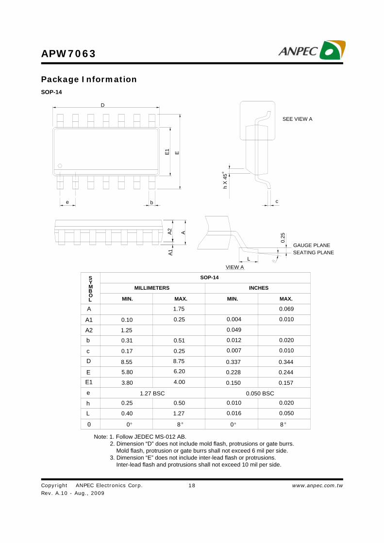
Package InformationSOP-14
SYMBOL MIN. MAX.
1.75
0.10
0.17 0.25
0.25
A
A1
c
D
E
E1
e
h
L
MILLIMETERS
b 0.31 0.51
SOP-14
0.25 0.50
0.40 1.27
MIN. MAX.
INCHES
0.069
0.004
0.012 0.020
0.007 0.010
0.010 0.020
0.016 0.050
0
0.010
1.27 BSC 0.050 BSC
A2 1.25 0.049
0° 8 ° 0° 8 °
L
VIEW A
0.25
SEATING PLANEGAUGE PLANE
Note: 1. Follow JEDEC MS-012 AB. 2. Dimension “D” does not include mold flash, protrusions or gate burrs. Mold flash, protrusion or gate burrs shall not exceed 6 mil per side. 3. Dimension “E” does not include inter-lead flash or protrusions. Inter-lead flash and protrusions shall not exceed 10 mil per side.
3.80
5.80
8.55
4.00
6.20
8.75 0.337 0.344
0.228 0.244
0.150 0.157
D
e b
E1 E
SEE VIEW A
c
h X
45°
A
A1
A2
Copyright ANPEC Electronics Corp.Rev. A.10 - Aug., 2009
APW7063
www.anpec.com.tw19
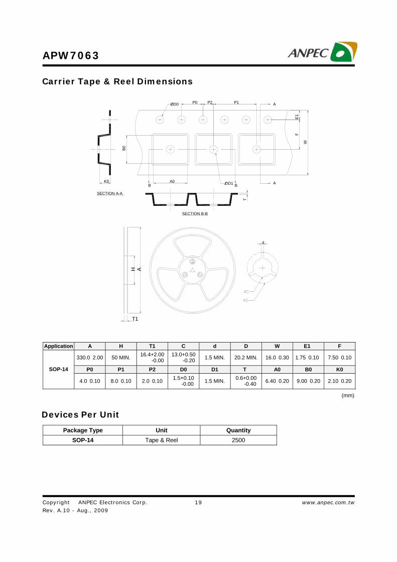
Application A H T1 C d D W E1 F
330.0±2.00 50 MIN. 16.4+2.00 -0.00
13.0+0.50 -0.20
1.5 MIN. 20.2 MIN. 16.0±0.30 1.75±0.10 7.50±0.10
P0 P1 P2 D0 D1 T A0 B0 K0 SOP-14
4.0±0.10 8.0±0.10 2.0±0.10 1.5+0.10 -0.00 1.5 MIN. 0.6+0.00
-0.40 6.40±0.20 9.00±0.20 2.10±0.20
(mm)
Carrier Tape & Reel Dimensions
H
T1
A
d
A
E1
AB
W
F
T
P0OD0
BA0
P2
K0
B0
SECTION B-B
SECTION A-A
OD1
P1
Package Type Unit Quantity
SOP-14 Tape & Reel 2500
Devices Per Unit

Copyright ANPEC Electronics Corp.Rev. A.10 - Aug., 2009
APW7063
www.anpec.com.tw20
Taping Direction InformationSOP-14
USER DIRECTION OF FEED
Classification Profile

Copyright ANPEC Electronics Corp.Rev. A.10 - Aug., 2009
APW7063
www.anpec.com.tw21
Classification Reflow ProfilesProfile Feature Sn-Pb Eutectic Assembly Pb-Free Assembly
Preheat & Soak Temperature min (Tsmin) Temperature max (Tsmax) Time (Tsmin to Tsmax) (ts)
100 °C 150 °C
60-120 seconds
150 °C 200 °C
60-120 seconds
Average ramp-up rate (Tsmax to TP) 3 °C/second max. 3°C/second max.
Liquidous temperature (TL) Time at liquidous (tL)
183 °C 60-150 seconds
217 °C 60-150 seconds
Peak package body Temperature (Tp)*
See Classification Temp in table 1 See Classification Temp in table 2
Time (tP)** within 5°C of the specified classification temperature (Tc)
20** seconds 30** seconds
Average ramp-down rate (Tp to Tsmax) 6 °C/second max. 6 °C/second max.
Time 25°C to peak temperature 6 minutes max. 8 minutes max.
* Tolerance for peak profile Temperature (Tp) is defined as a supplier minimum and a user maximum. ** Tolerance for time at peak profile temperature (tp) is defined as a supplier minimum and a user maximum.
Table 2. Pb-free Process – Classification Temperatures (Tc)
Package Thickness
Volume mm3 <350
Volume mm3 350-2000
Volume mm3 >2000
<1.6 mm 260 °C 260 °C 260 °C 1.6 mm – 2.5 mm 260 °C 250 °C 245 °C
≥2.5 mm 250 °C 245 °C 245 °C
Table 1. SnPb Eutectic Process – Classification Temperatures (Tc)
Package Thickness
Volume mm3
<350 Volume mm3
≥350 <2.5 mm 235 °C 220 °C ≥2.5 mm 220 °C 220 °C
Test item Method Description SOLDERABILITY JESD-22, B102 5 Sec, 245°C HOLT JESD-22, A108 1000 Hrs, Bias @ 125°C PCT JESD-22, A102 168 Hrs, 100%RH, 2atm, 121°C TCT JESD-22, A104 500 Cycles, -65°C~150°C HBM MIL-STD-883-3015.7 VHBM≧2KV MM JESD-22, A115 VMM≧200V Latch-Up JESD 78 10ms, 1tr≧100mA
Reliability Test Program

Copyright ANPEC Electronics Corp.Rev. A.10 - Aug., 2009
APW7063
www.anpec.com.tw22
Customer Service
Anpec Electronics Corp.Head Office :
No.6, Dusing 1st Road, SBIP,Hsin-Chu, Taiwan, R.O.C.Tel : 886-3-5642000Fax : 886-3-5642050
Taipei Branch :2F, No. 11, Lane 218, Sec 2 Jhongsing Rd.,Sindian City, Taipei County 23146, TaiwanTel : 886-2-2910-3838Fax : 886-2-2917-3838