Embed Size (px)
Citation preview

Shanhui Fan
Department of Electrical Engineering
Stanford University
Stanford, CA 94305
Email: [email protected]
http://www.stanford.edu/~shanhui/
Applying sub-wavelength electromagnetics and
nanophotonics for energy conversion and transfer

Maxwell’s equations and large-scale computation
EB
t
HD
tJ
http://www.psc.edu/machines/sgi/uv/black
light_crpd.jpg

Outline
Nanophotonic light trapping Wireless energy transfer

TCO
a-Si
Ag
Si thickness
280nm
Nanodome a-Si Cell
With Y. Cui’s group at Stanford

Full absorption
depth ~ 1000nm
Carriers only travel
for 200-300nm
Nanophotonic light management:
• Absorb light efficiently in a layer that is as thin as possible.
• Reduce material cost.
• Facilitate carrier extraction.
Challenges of light management for a-Si cell

Simulated nanodome geometry
a-Si

Simultaneous Light Trapping and Anti-Reflection
= 450nm = 750nm
Anti-reflection Light trapping

Nanocone
J. Zhu, Z. Yu, G. Burkhard, C. Hsu, S. Connor, Y. Xu, Q. Wang, M. Mcgehee, S. Fan, Y. Cui, Nano Letters 9, 279 (2009).
Success in combining theory and experiments

TCO
a-Si
Ag
Si thickness
280nm
Nanodome a-Si Cell

J. Zhu, C.M. Hsu, Z. Yu, S. Fan, Y. Cui, Nano Letters 10,1979 (2010).
-0.2 0.0 0.2 0.4 0.6 0.8-20
-15
-10
-5
0
5
Cu
rren
t (m
A/c
m2)
Voltage (V)
-0.2 0.0 0.2 0.4 0.6 0.8-20
-15
-10
-5
0
5
Cu
rre
nt
(mA
/cm
2)
Voltage (V)
Thin Film Nanodome
Jsc= 11.4mA/cm2 Jsc= 17.5mA/cm2
Very significant improvement in short-circuit current
- Latest results, with simultaneous electronic and optical optimization, has pushed
efficiency to 9.7%.

Simultaneous Light Trapping and Anti-Reflection
= 450nm = 750nm
Anti-reflection Light trapping

An important theoretical question
• What is the fundamental limit of absorption enhancement
using light trapping in solar cells?
A. Goetzberger IEEE Photovoltaic Specialists Conference (1981).
Optical confinement in thin Si-solar cells by diffuse back reflectors
E. Yablonovitch J. Opt. Soc. Am. A (1982).
Statistical ray optics
P. Campbell & M. Green J. Appl. Phys. (1986).
Light trapping properties of pyramidally textured surface
Classical Light Trapping Theory
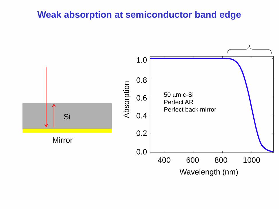
50 m c-Si
Perfect AR
Perfect back mirror
0.2
0.4
0.6
0.8
1.0
0.0 400 600 800 1000
Wavelength (nm)
Absorp
tion
Weak absorption at semiconductor band edge
Si
Mirror

The Yablonovitch Limit
Si
Mirror sin 1 1
n
Maximum absorption enhancement factor
Derived with a ray tracing argument
4n2
E. Yablonovitch, J. Opt. Soc. Am. 72, 899 (1982); Goetzberger, IEEE Photovoltaic
Specialists Conference, p. 867 (1981); Campbell and Green, IEEE Trans. Electron.
Devices 33, 234 (1986).

Nanocone
J. Zhu, Z. Yu, et al, Nano Letters 9, 279 (2009).
From conventional to nanoscale light trapping
50 m
500 nm
Ray tracing Wave effect is important
M. Green (2001)

Light Trapping With Grating
mirror
Active layer
500nm

Absorption enhanced by guided resonance
• Guided resonance peak.
• Narrow spectral width for each peak.
• Requires aggregate contribution of large number of resonances.

Statistical Temporal Coupled Mode Theory
Instead of thinking about rays Think about many resonances
Zongfu Yu, Aaswath Raman, and Shanhui Fan Proceedings of the National Academy of Sciences 107,17491 (2010).

A single resonance
Resonant frequency
absorp
tion

Radio a
Radio b Radio c
88.5 MHz 97 MHz 106 MHz
Covering the broad solar spectrum with multiple
resonances

Sum over multiple resonances
M resonances
m
m

M resonances
N channels
Multiple plane channels in free space
max
M
N2 i
Take into account diffraction in free space

=
M
N2
i
Theory for nanophotonic light trapping
Number of resonances in the structure: M
Number of plane wave channels in free
space: N
Maximum absorption over a particular
bandwidth
=
M
N2
i
Zongfu Yu, Aaswath Raman, and Shanhui Fan Proceedings of the National Academy of Sciences 107,17491 (2010).

Reproducing the Yablonovitch Limit (the math)
Random texture can be
understood in terms of grating
with large periodicity
Conventional limit
Large Periodicity L >>
Large Thickness d >>
=
M
N2
i F / d =4n2
L
d
Maximum absorption Maximum enhancement factor

The intuition about the Yablonovitch limit from the
wave picture
FM
Nd
Number of resonance in the film
Thickness of the film
When the thickness d
Double the thickness doubles the number of the resonances

The key in overcoming the Yablonovitch limit
FM
Nd
Number of resonance in the film
Thickness of the film
Nanoscale modal confinement over broad-bandwidth

Light Scattering Layer = 12.5, t = 80nm
Light Confining Layer = 12.5, t = 60nm
Light Absorption Layer = 2.5, = 400 cm-1, t = 5nm
Mirror
Light confinement in nanoscale layers

60n2
Light intensity distribution
5nm thick
15 times of the classical limit
Enhancement: 15 times the classical limit

Zongfu Yu, Aaswath Raman, and Shanhui Fan Proceedings of the National Academy of Sciences 107,17491 (2010).
Red: 4n2 limit
Simulated Absorption Spectrum
4n2
Enhancement Factor Angular Response

Application to organic solar cell structure
PCDTBT:PCBM PEDOT:PSS
TiOx
Al
ITO ITO
Increase the number of optical modes to enhance light absorption
Top layer
Side view
A. Raman, Z. Yu and S. Fan, Optics Express 19, 19015 (2011).

Outline
Nanophotonic light trapping Wireless energy transfer

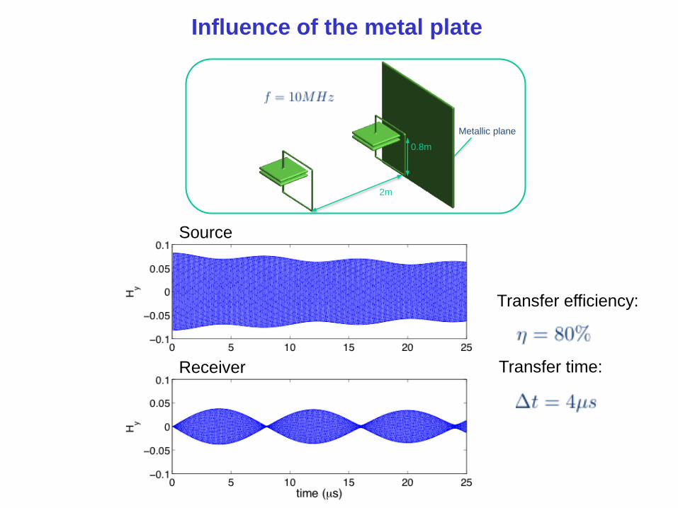
f = 10MHz, d = 2m, P = 60W, efficiency = 40%
A. Kurs et al. Science, vol. 317 (2007) pp 83-86
Previous Experiment

Wireless energy transfer into moving vehicles:
Complex EM environment (metallic car body).
High power (on the order of 10kW).
Moving (transfer distance might vary).
Challenges
Collaboration with
Dr. S. Beiker, Dr. R. Sassoon

2m
0.8m
Monitor point
Monitor point
Magnetic dipole
source
Wireless Energy Transfer in Free Space
Transfer efficiency:
Transfer time:
Source
Receiver
2m
0.8m
Metallic plane
Influence of the metal plate
Transfer efficiency:
Transfer time:
Source
Receiver

2m
0.8m
Optimized design incorporating metal plate
Transfer efficiency:
Transfer time:
Source
Receiver

Efficient transfer over 2 meter
Distance (m)
1 2 3
100
80
60
40
20
0
Eff
icie
ncy
97%

Summary
Nanophotonic light trapping Wireless energy transfer
Z. Yu, A. Raman
Prof. Y. Cui
X. Yu, S. Sandhu
Dr. S. Beiker, Dr. R. Sassoon
Poster # 33