Embed Size (px)
Citation preview

Lecture 17, p 1
Semiconductors, intrinsic and doped
Reference for this Lecture:
Elements Ch 12
Reference for Lecture 19:
Elements Ch 13
Lecture 17
Applications of Free Energy Minimum

Lecture 17, p 2
Thumbnail review of free energy:
Equilibrium corresponds to maximum Stot = Sreservoir + Ssmall system.
When we calculate ∆S, we only need to know the temperature of the reservoir. In
minimizing F (equivalent to maximizing Stot) we don’t have to deal explicitly with Sreservoir .
Consider exchange of material (particles) between two containers.
These are two small systems in equilibrium with a reservoir
(not shown) at temperature T. In equilibrium, dF/dN1 = 0:
The derivative of free energy with respect to particle number is
so important that we define a special name and symbol for it:
For two subsystems exchanging
particles, the equilibrium condition is:
Last Time
Maximum Total Entropy Minimum Free Energy Equal chemical potentials
1 2 1 2
1 1 1 1 2
1 2
1 2
0dF dF dF dFdF
dN dN dN dN dN
dF dF
dN dN
= + = − =
=
1N
F = F1+F2
N1 N2
The chemical potential of subsystem “i”i
i
i
dF
dNµ ≡
1 2µ µ=

Lecture 17, p 3
Electrons in Semiconductors
In many materials, electrons cannot have every conceivable energy. There
is a low energy range (the “valence band”) and a high energy range (the
“conduction band”). A “gap” of disallowed energies separates them. (The
reason for the gap is a Physics 214 topic.)
At T = 0, every valence band state is occupied. At T ≠ 0, electrons are
thermally excited from the valence band to the conduction band. How many
determines the electrical conductivity.
The activated free electrons and the “holes” (unfilled states) left behind act
as two ideal gases. We can compute the density of thermally excited
electrons (and holes) by minimizing Felectron + Fhole .
Here, to simplify the problem we assume that excitation from valence to
conduction band always requires the same energy, i.e., every conduction
state has energy ∆ more than every valence state. This avoids having to do
integrals.
Energy gap, ∆
At T = 0:
Conduction band has no electrons
Valence band totally filled with electrons

Lecture 17, p 4
Electrons in Semiconductors (2)
This is Shockley’s* cartoon of an intrinsic semiconductor.
At T = 0, the cars (electrons) can’t move. If some are
raised to the upper level (the conduction band) then
motion becomes possible.
The vacant spaces on the lower level are “holes”. Motion
of the cars on the lower level is more simply described by
pretending that the holes are the objects that move.
*John Bardeen, Walter Brattain, and William Shockley invented the transistor in 1947.
Conduction electron
Hole
An intrinsic semiconductor is
one in which the number of
electrons equals the number
of valence band states, so that
at T = 0 every state is filled,
and no electrons are left over.

Lecture 17, p 5
We have
N electrons
N valence states (call their energy zero)
N conduction states (energy ∆)
We want to know
Ne and Nh,
the numbers of conduction electrons and holes at temperature T
Our analysis will be similar to the “Defects in a Lattice” problem.
Conduction electrons and holes are created in pairs, so: Ne = Nh (and dNe = dNh )
Method: Minimize F = Fe + Fh:
Conduction electron
∆
hole
0h e
µ µ+ === + → +d= 0e hN dNe eh h
e e e e h
dF dFdF dFdF
dN dN dN dN dN
Intrinsic Semiconductors
One big difference: electrons and holes actually behave like ideal gases --they are
free to rapidly move around in the crystal, with an “effective mass” me, mh.
So, what are S, F, and µ for an Ideal Gas of Particles?

Lecture 17, p 6
How Do S, F, µ Depend on N/V?
In general, this is a complicated function of particle properties and the
environment. To keep things simple, we’ll only work with ideal gases.
For an ideal gas the internal energy per particle, u ≡ U/N, depends on T,
but not on N. For many problems we can set this to 0.
How does S depend on N? Let’s count microstates and see.
Thus,
and the chemical potential for an ideal (monatomic) gas is:
n ≡ N/V = particle density, nQ ≡ M/V = number of states per unit volume.
nQ can only be calculated using quantum mechanics, so we will treat
it as an empirical quantity (i.e., we’ll tell you the numerical value when
necessary). nQ is a function of T, but not of the particle density, n.
( )Ω = = = − so ln( ) ln ln ! ! !
N NM M
S k k N M NN N
The number of “bins”,
M, is proportional to V.
It also depends on T
(see next slide).
µ ∂ ∂ ≡ = − = − = + = + ∂ ∂ ,
Sln ln ln
NV T M Q Q
F M N nu T u kT u kT u kT
N N Vn n
∂ = = ∂
S (ln !)ln since ln
NM
M d Nk N
N dN
For ideal gases,
µ ~ logarithm of
particle density.

Lecture 17, p 7
number of states in volume V
number of particles
Q Qn n V
n N= =
Considering both
position and
momentum.
What is nQ?nQ = total no. states (per unit volume) available to a particle at temp. T
QM: particle with momentum p has wavelength λ = h/p. (h = Plank’s constant)
Taking λ as a characteristic length, the effective cell volume is ~∆V ≈ λ3 = (h/p)3.
Using p2/2m = (3/2)kT, the quantum-mechanical ‘cell density’ has a T-dependence:
nQ ≈ 1/λ3 = (3mkT/h2)3/2
2 3 / 2 30 3 3 / 2 3 / 2(2 / ) (10 )( / ) ( / 300 )Q pn mkT h meter m m T Kπ −= =
Examples:30 3 3/ 2 3/ 2 30 3(H @ 300K) (10 meter )( / ) ( / 300 ) 10 meterQ pn m m T K− −= =
30 3 3/2 3/2 30 3(He @ 300K) (10 meter )(4 / ) (300 / 300 ) 8 10 meterQ p pn m m K− −= = ×
*For a monatomic gas, the nT(T) we had before is nQ; otherwise there are modifications.
If we do the problem more carefully (see Elements for details) we find*
30 3 3/2 3/2 27 3( e @ 3K) (10 meter )(4 / ) (3 / 300 ) 8 10 meterQ p pn H m m K− −= = ×
Lecture 17, p 8
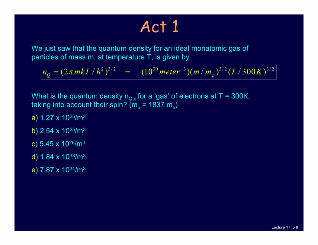
We just saw that the quantum density for an ideal monatomic gas of
particles of mass m, at temperature T, is given by
What is the quantum density nQ,e for a ‘gas’ of electrons at T = 300K,
taking into account their spin? (mp = 1837 me)
a) 1.27 x 1025/m3
b) 2.54 x 1025/m3
c) 5.45 x 1026/m3
d) 1.84 x 1033/m3
e) 7.87 x 1034/m3
Act 1
2 3 / 2 30 3 3 / 2 3 / 2(2 / ) (10 )( / ) ( / 300 )Q pn mkT h meter m m T Kπ −= =

Lecture 17, p 9
We just saw that the quantum density for an ideal monatomic gas of
particles of mass m, at temperature T, is given by
What is the quantum density nQ,e for a ‘gas’ of electrons, taking into
account their spin? (mp = 1837 me)
a) 1.27 x 1025/m3
b) 2.54 x 1025/m3
c) 5.45 x 1026/m3
d) 1.84 x 1033/m3
e) 7.87 x 1034/m3
Solution
If we have more complicated particles (e.g., diatomic molecules that can
rotate), this will also increase the quantum density.
See Textbook for more details.
2 3 / 2 30 3 3 / 2 3 / 2(2 / ) (10 )( / ) ( / 300 )Q pn mkT h meter m m T Kπ −= =
A direct calculation using the above formula would
give choice a). But we also need to take into
account that every electron spin could be either up
or down, i.e., increasing the number of states by a
factor of 2.

Lecture 17, p 10
We now have the tools to solve for the equilibrium density of e-h pairs:
1. Since they act like ideal gases, the chemical potentials are
2. Electrons and holes are created in pairs total free energy is minimized when
3. For a pure semiconductor, ne = nh = ni (“intrinsic pair density”)
Electrons and holes in Semiconductors
Energy gap, ∆
At T = 0:
Conduction band has no electrons
Valence band totally filled with electrons
µ
= ln h
h
Qh
nkT
nµ
= ∆
+ ln e
e
Qe
nkT
n
E = ∆
E = 0
µ µ
+ = = + ∆ + = ∆ +
0 ln ln lne h eh
h e
Qh Qe Qh Qe
n n nnkT kT kT
n n n n
nQ = (geometric mean of nQenQh) ≡ (nQenQh)1/2
.
Compare to I-V result (p. 11).
−∆ −∆ −∆= ⇒ = = ⇒ =
2
2ln h e h e i ikT kT
Qh Qe Qh Qe Qh Qe Q
n n n n n ne e
n n kT n n n n n

Lecture 17, p 11
≡ -∆/2kT
e h i Q n = n n = n e
E-h pair density vs. T
In a pure semiconductor, there are equal numbers of
conduction-band electrons and valence-band holes:
This “intrinsic density” ni clearly varies strongly with
energy gap.
Some numerical values (at T = 300 K):
material ∆(eV) nQ (meter-3) ni (meter-3)
Si 1.14 1.72 x 1025 5.2 x 10¹⁵
Ge 0.67 7.21 x 1024 -
GaAs 1.43 2.63 x 1024 -
Question:
Why aren’t the nQ all equal? In particular, if you set m = me in the formula, nQ= 1.27×1025.
The answer is that the effective mass of a hole is not equal to the effective mass of an
electron (and even me,effective≠ me 9.11 x 10⁻³¹kg!), due to interactions with the lattice.
Therefore, we will treat nQ as an empirical quantity.

Lecture 17, p 12
Exercise: Intrinsic Silicon
At 300 K the intrinsic carrier density in Si is ni= 5.2 x 10¹⁵/m3, with a
bandgap of ∆ = 1.14 eV, and quantum density nQ
= 1.72 x 1025/m3.
What is the carrier density at 150 K?
a. 4.3 × 10⁵/m3 b. 3.4 × 10¹⁰/m3 c. 2.6 × 10¹⁵/m3
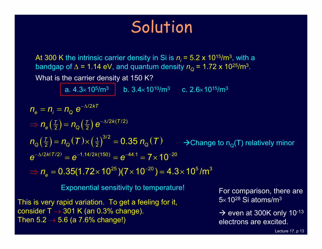
Lecture 17, p 13
Solution
Exponential sensitivity to temperature!
( ) ( )( ) ( ) ( ) ( )
( )
−∆
−∆
−∆ − − −
−
= =
=
= × =
= = = ×
= × × =
⇒
⇒ ×
/2
/2 ( /2)
2 2
3/21
2 2
/2 /2 1.14/2 (150) 44.1 20
25 20 5 3
0.35
7 10
0.35(1.72 10 )(7 10 ) 4.3 10 /m
kT
e i Q
k TT T
e Q
T
Q Q Q
k T k
e
n n n e
n n e
n n T n T
e e e
n
Change to nQ(T) relatively minor
This is very rapid variation. To get a feeling for it,
consider T → 301 K (an 0.3% change).
Then 5.2 → 5.6 (a 7.6% change!)
At 300 K the intrinsic carrier density in Si is ni= 5.2 x 10¹⁵/m3, with a
bandgap of ∆ = 1.14 eV, and quantum density nQ
= 1.72 x 1025/m3.
What is the carrier density at 150 K?
a. 4.3×10⁵/m3 b. 3.4×10¹⁰/m3 c. 2.6×10¹⁵/m3
For comparison, there are
5×1028 Si atoms/m3
even at 300K only 10-13
electrons are excited.

Lecture 17, p 14
Digital Thermometers
The rapid (exponential) variation of resistance with temperature is used to measure temperature. Many modern digital thermometers use a “thermistor”, a semiconductor device whose resistance depends on temperature.

Lecture 17, p 15
Act 2: Other Semiconductors
Compare the number of intrinsic carriers in the conduction band, ni, for Si, Ge
and GaAs at 300 K. Note: kT = 0.026eV at T = 300K.
Some numerical values (at T = 300 K):
material ∆(eV) nQ (meter-3) ni (meter-3)
Si 1.14 1.72 x 1025 5.2 x 10¹⁵
Ge 0.67 7.21 x 1024 -
GaAs 1.43 2.63 x 1024 -
a) ni,Si > ni,GaAs > ni,Ge
b) ni,Si > ni,Ge > ni,GaAs
c) ni,Ge > ni,Si > ni,GaAs

Lecture 17, p 16
Act 2: Other Semiconductors
Compare the number of intrinsic carriers in the conduction band, ni, for Si, Ge
and GaAs at 300 K. Note: kT = 0.026eV at T = 300K.
Some numerical values (at T = 300 K):
material ∆(eV) nQ (meter-3) ni (meter-3)
Si 1.14 1.72 x 1025 5.2 x 10¹⁵
Ge 0.67 7.21 x 1024 -
GaAs 1.43 2.63 x 1024 -
a) ni,Si > ni,GaAs > ni,Ge
b) ni,Si > ni,Ge > ni,GaAs
c) ni,Ge > ni,Si > ni,GaAs
0.67 / 2 0.026 19 3
24 3
1.43 / 2 0.026 12 3
24 3
Ge: 1.8 10 /m
using 7.2 10 /m
GaAs: 3.0 10 /m
using 2.6 10 /m
eV eV
i Q
Q
eV eV
i Q
Q
n n e
n
n n e
n
− ×
− ×
= = ×
= ×
= = ×
= ×
The difference is
almost entirely due
to the band gap.

Lecture 17, p 17
At T = 0, in a pure semiconductor the valence band is completely filled with
electrons, and there are none in the conduction band. Suppose we replace one
Si atom with a P atom. Phosphorous has one more electron, which is very weakly
bound (its ∆ is very small), and will almost certainly end up in the conduction
band. Think of Shockley’s garage. If we add one car, it will have to go into the
upper level, and there are still no vacancies (holes) in the lower level.
Phosphorus is called a “donor atom”.
The addition of impurities that have a
different number (more or fewer) of
valence electrons is called doping.
It can have a dramatic effect on the
material’s electrical properties.
With doping, we no longer have Ne = Nh.
Instead, N’e= N’h + Nd, where Nd is the number of donor atoms.
Silicon (Group IV)
Phosphorous (Group V)
Si
Si
Si Si
Si
Si
Si Si Si
Si
P An extra (free) electron.
No extra hole.
Doping of Semiconductors
More of Shockley’s cartoon

Lecture 17, p 18
2. We can also replace Si atoms with Al. Aluminum has one fewer electron than
silicon. What is the relation between Ne and Nh in this case?
a) Ne = Nh - NAl b) Ne = Nh c) Ne = Nh + NAl
Silicon (Group IV)
Aluminum (Group III)
Si
Si
Si Si
Si
Si
Si Si Si
Si
Al
Act 31. There are 5×1028 Si atoms/m3. At 300 K, ni,Si = 5.2 x 10¹⁵/m3. If we replace one
out of every million Si atoms with P, how much will the conductivity increase?
a) 104 b) 106 c) 107

Lecture 17, p 19
2. We can also replace Si atoms with Al. Aluminum has one fewer electron than
silicon. What is the relation between Ne and Nh in this case?
a) Ne = Nh - NAl b) Ne = Nh c) Ne = Nh + NAl
Silicon (Group IV)
Aluminum (Group III)
Si
Si
Si Si
Si
Si
Si Si Si
Si
Al
Solution1. There are 5×1028 Si atoms/m3. At 300K, ni,Si = 5.2 x 10¹⁵/m3. If we replace one
out of every million Si atoms with P, how much will the conductivity increase?
a) 104 b) 106 c) 107
ne = ni + nd = ni + 10-6 nSi ≈ 10-6 nSi = 5 x 10²²/m3, 7 orders of magnitude more than
with no doping.
Lecture 17, p 20
2. We can also replace Si atoms with Al. Aluminum has one fewer electron than
silicon. What is the relation between Ne and Nh in this case?
a) Ne = Nh - NAl b) Ne = Nh c) Ne = Nh + NAl
Silicon (Group IV)
Aluminum (Group III)
Si
Si
Si Si
Si
Si
Si Si Si
Si
Al
Solution
We are missing some valence electrons, so even when Ne (electrons in the
conduction band) is zero, we have one hole per Aluminum atom.
Look at the “p-type” part of Shockley’s cartoon.
Aluminum is called an “acceptor atom”. In the equations, acceptors act like
negative Nd.
1. There are 5×1028 Si atoms/m3. At 300K, ni,Si = 5.2 x 10¹⁵/m3. If we replace one
out of every million Si atoms with P, how much will the conductivity increase?
a) 104 b) 106 c) 107
ne = ni + nd = ni + 10-6 nSi ≈ 10-6 nSi = 5 x 10²²/m3, 7 orders of magnitude more than
with no doping.

Lecture 17, p 21
We can follow the same procedure to minimize the free energy.
Assume nd<<nQ. (This is called “light doping”.) ∆F = 0 implies that µe + µh = 0.
This is again like the vacancy-interstitial problem.
Solution: or nenh = ni2
Typically, nd >> ni. Therefore ne = ni + nd ≈ nd.
Almost all of the “free” (conduction) electrons come from the dopant atoms.
For Si at T = 300 K:
If there were no doping, both ne/nQ and nh/nQ would be ~3×10⁻⁹.
Even a small amount of doping: nd/nQ = 10-7, increases ne dramatically
and suppresses nh. ne/nQ ~ 10-7, nh/nQ ~ 10-12.
In the I-V problem, adding interstitial atoms to a crystal reduces the number of vacancies.
∆−=
2
e h kT
Q
n ne
n
Doping of Semiconductors (2)
+ = ∆ + + =ln( ) ln( ) 0e h
e h
Qe Qh
n nkT kT
n nµ µ
ne = nh + nd
Assume: ne and nh << nQ.
This is an example of “the law of mass action”.
“intrinsic pair density” ni = ne = nh
nQ= (nQenQh)1/2
−≈ 19
2 10e h
Q
n n
n
Lecture 17, p 22
−∆∆ = → + = → = 2 /
e0 0 kT
h e h QF n n n eµ µ
if ne and nh << nQ.
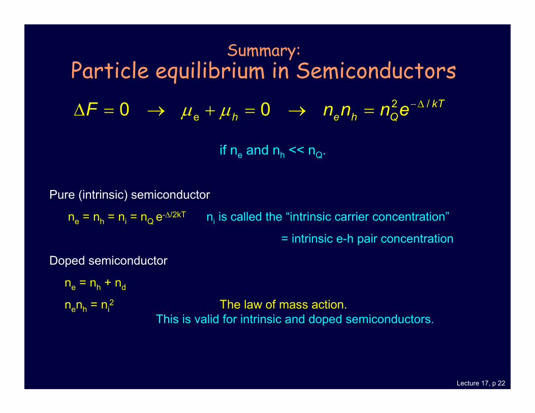
Pure (intrinsic) semiconductor
ne = nh = ni = nQ e-∆/2kT ni is called the “intrinsic carrier concentration”
= intrinsic e-h pair concentration
Doped semiconductor
ne = nh + nd
nenh = ni2 The law of mass action.
This is valid for intrinsic and doped semiconductors.
Summary:
Particle equilibrium in Semiconductors

Lecture 17, p 23
Example: Law of Mass Action
The addition of impurities increases the crystal’s conductivity. Let’s add
nd = 1024/m3 phosphorous atoms to Si. Using the intrinsic carrier density, nI,
that we calculated for silicon, compute the density of holes, nh , in this
“doped” crystal.

Lecture 17, p 24
nI = 5.2×10¹⁵ << nd, so ne ≈ nd.
This doping overwhelms the intrinsic carrier density.
ne ≠ nh, but nenh = ni2 still holds.
The addition of electrons has depressed the density of holes by over
8 orders of magnitude!
Solution
( )2152
7 3
24
5 2 102 7 10 /m
1 10i
h
e
.nn .
n
×= = = ×
×Law of Mass Action ⇒
Question: Is 1024 atoms/m3 a lot or a little?
Hint: There are 5×1028 Si atoms/m3.
The addition of impurities increases the crystal’s conductivity. Let’s add
nd = 1024/m3 phosphorous atoms to Si produces. Using the intrinsic carrier
density, nI, that we calculated for silicon, compute the density of holes, nh ,
in this “doped” crystal.

Lecture 17, p 25
Act 4
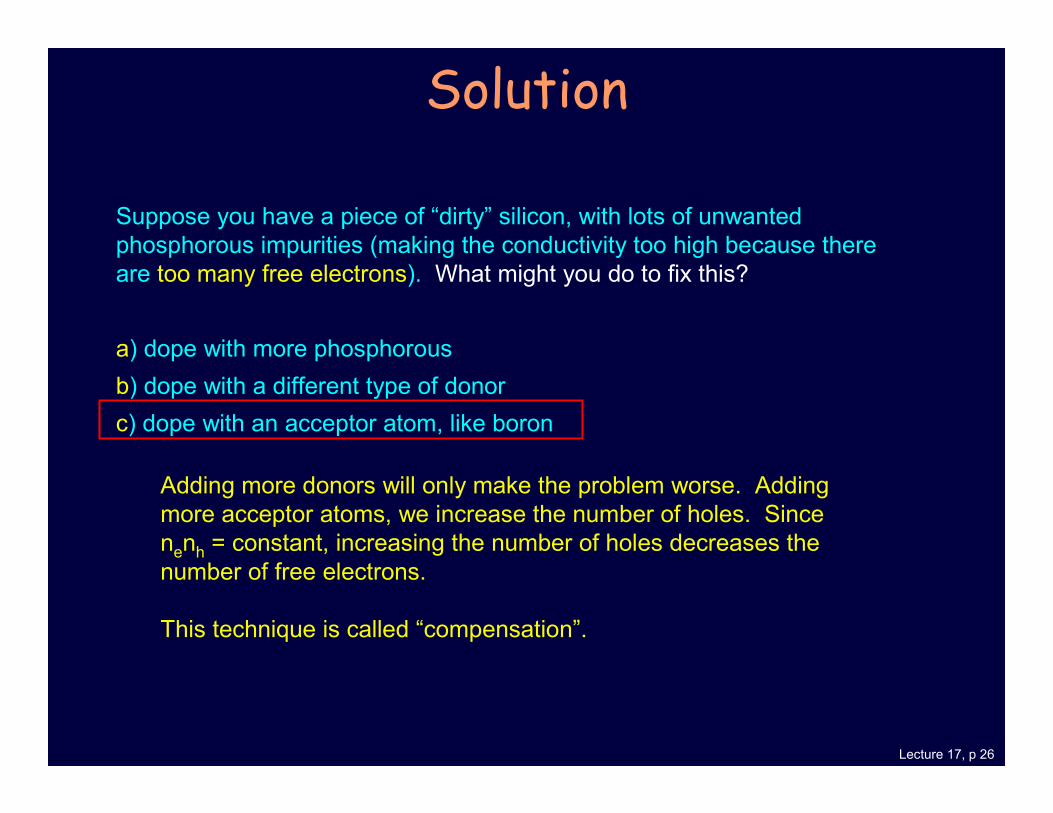
Suppose you have a piece of “dirty” silicon, with lots of unwanted
phosphorous impurities (making the conductivity too high because there
are too many free electrons). What might you do to fix this?
a) dope with more phosphorous
b) dope with a different type of donor
c) dope with an acceptor atom, like boron
Lecture 17, p 26
Solution
Suppose you have a piece of “dirty” silicon, with lots of unwanted
phosphorous impurities (making the conductivity too high because there
are too many free electrons). What might you do to fix this?
a) dope with more phosphorous
b) dope with a different type of donor
c) dope with an acceptor atom, like boron
Adding more donors will only make the problem worse. Adding
more acceptor atoms, we increase the number of holes. Since
nenh = constant, increasing the number of holes decreases the
number of free electrons.
This technique is called “compensation”.
Lecture 17, p 27
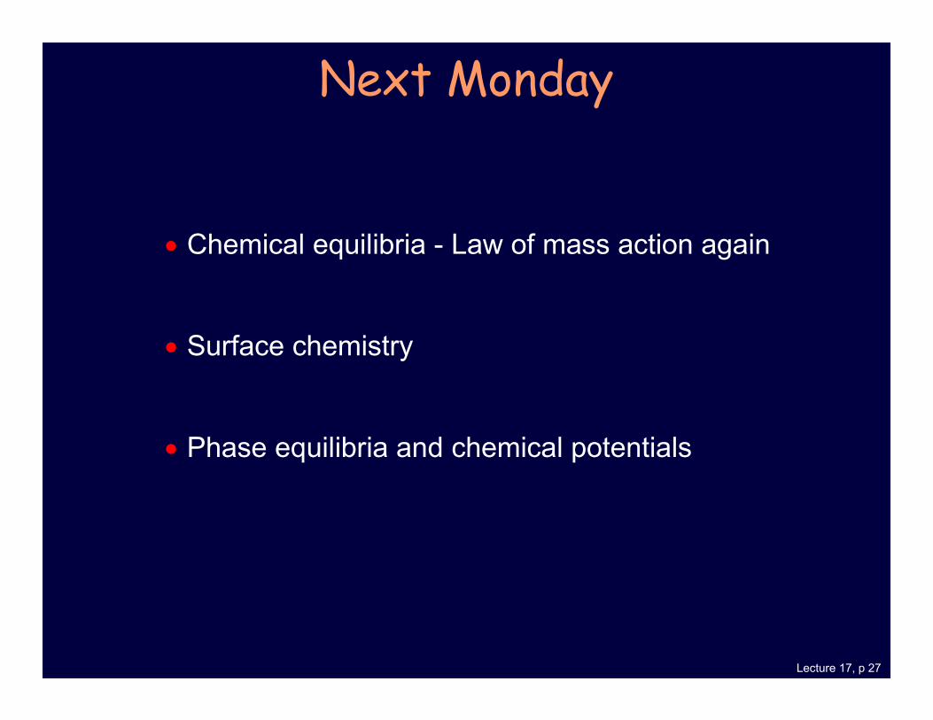
Next Monday
• Chemical equilibria - Law of mass action again
• Surface chemistry
• Phase equilibria and chemical potentials