Embed Size (px)
Citation preview

Application of theUKRAA Very Low Frequency Receiver System
Whitham D. ReeveAnchorage, Alaska USA
Member, Society of Amateur Radio Astronomers
Abstract: Members of the UK Radio Astronomy Associationhave been working on a VLF receiver system prototypedesign since 2006 and UKRAA now sells it in kit and builtform. The system consists of three major components: VLFreceiver, 0.4 m square loop antenna, and antenna tuningunit. A signal generator also is available for testing andtuning the receiver. This paper discusses: 1) Receiver systemarchitecture and characteristics; and 2) Kit constructiondetails.
Note: The original intent of this paper was to include a thirdpart – 3) Performance in my observatory in Anchorage,Alaska USA – but local interference conditions preventedreception during SID events and there is nothing to report.
I. INTRODUCTION
The Very Low Frequency (VLF) receiver system is auseful sensor for monitoring Sudden IonosphericDisturbances (SID) caused by solar flares. It does notreceive solar radio emissions directly. Instead, it receivesterrestrial transmissions that propagate in an Earth-ionosphere waveguide, which is affected by solar flares.Solar flares change the waveguide’s propagationcharacteristics and, thus, are indirectly observable withthe receiver.
A number of inexpensive VLF receiver designs haveappeared over the years, many of them designed by radioamateurs and experimenters (for example, some of thepopular ones are [1,2,3,4]). Few of these receiver designswere based on a systems approach and some sufferedserious limitations. Many of the designs focused only onthe receiver with little attention to the other parts of thereceiving system. A few were available as kits or alreadybuilt. Yet other receivers (for example, the SolarSID andSuperSID [5]) were specifically designed for educationalpurposes.
In contrast, the UK Radio Astronomy Association(UKRAA)1 receiver is part of a modular system. Thesystem also includes a loop antenna, antenna tuning unit
1The UKRAA (www.ukraa.com) is the commercial arm of
the British Astronomy Association (BAA) Radio AstronomyGroup (RAG). The BAA is the parent body of additionalastronomy groups. For additional information:www.britastro.org.
(ATU) and signal generator for testing and alignment. Ithas provisions for a built-in analog-digital converter(ADC), addressable Inter-Integrated Circuit (I2C)2 busconnection to an optional external controller, and on-board temperature sensor. Of course, some method oflogging the receiver output also is required. The UKRAAreceiver has two analog outputs as well as an ADC outputthat is compatible with Radio-SkyPipe software but,unfortunately, requires the obsolete parallel printer port.3
The UKRAA VLF receiver system is available as a kit oralready built, catering to both experimenters and otherswho would like to start using the receiver immediately.The kits can be assembled by inexperienced builders withrelatively simple tools and test equipment. Systemmodules can be purchased as needed (Table 1).
Table 1- VLF receiver prices (current as of Dec 2009)
Description Price (GBP) Price (US$)VLF receiver kit,no enclosure
60.00 ~96.00
VLF receiver assembled,no enclosure
90.00 ~143.00
VLF receiver, assembledwith enclosure
120.00 ~191.00
Loop antenna kit, no wire 15.00 ~24.00Loop antenna kit, with wire 31.00 ~49.00Loop antenna, assembled 35.00 ~56.00Antenna tuning unit,assembled
25.00 ~40.00
VLF signal generator,23.4 kHz
15.00 ~24.00
Prices do not including shipping from UK to destinationTo order, send inquiry to [email protected]
II. RECEIVER SYSTEM CHARACTERISTICS
A. System block diagram
An overall block diagram reveals the system components(Fig. 1). The major components are antenna, antennatuning unit, receiver, and measurement device. Optionalcomponents (not required for operation) are controller and
2For additional information: http://www.i2c-bus.org/.
3The persistent use of the parallel port by many amateur radio
astronomers is universally justified by their claim that “everyonehas an old PC lying around with a parallel printer port.”

signal generator. The controller is another UKRAAhardware development project as is the Starbase softwaresystem that can be used with a number of controllers andassociated sensors, including VLF receivers andgeomagnetometers.
Fig. 1 – Overall system block diagram
The receiver system can be connected to an external dcvoltmeter for real-time display or, more commonly, to adatalogger for charting and data archiving. The overallsystem design is based on considerable experimentationby various UKRAA members and incorporates circuitsfrom published and unpublished projects by others.
B. Loop antenna
1. Configuration: The UKRAA antenna is a square loopwith 0.4 m sides (Fig. 2). It has a hardwood cross-beamstructure and consists of 125 turns of magnet wire (wirecan be optionally purchased with the antenna kit or userscan supply their own). The loop is supported by aplywood base.
2. Characteristics: The loop characteristics are:
Parameter ValueDimensions 0.4 mWire 24 AWGTurns 125Inductance 22.5 mHResistance (dc) 17.1 ohms at 21 CQ 50Self-resonant frequency 52.2 kHz
Note: Q and self-resonant frequency measured for a137 turn loop antenna
Fig. 2 – UKRAA loop antenna posing with the antenna tuning unit (justbelow bottom corner of loop) and unrelated equipment
Loop frame and base construction was fast and simple,consisting of only a few pre-cut wood components thatare glued together. After the glue cured overnight, aprotective varnish was applied and allowed to cure. Thenthe windings were placed using the shop winding table(Fig. 3).
Fig. 3 – Loop antenna frame (left) on the shop winding table. The tableis the square rotating platform with a mandrel directly under the frameand placed on a Workmate® bench. Winding 125 turns from the wire
spool (right) required approximately 20 minutes
2. Inductance: For reference, the approximate inductance,in H, of a polygon coil with rectangular cross-section isgiven by4
4Eq. 157, pg 257, Circular C74, Radio Instruments and
Measurements, US Department of Commerce, National Bureauof Standards, 1937. The units specified in the original source areused in this analysis.

201257.0 naL
d
a
a
c
a
b 8log
96321303.2
2
2
2
2
22
2
116
ya
by
whereL inductance (H)a average of inscribed and circumscribed radii,
Nr
2cos2
(cm)
r radius of circumscribed circle (cm)N number of polygon sides (4 for square)b axial dimension of the coil cross-section (cm)c radial dimension of the coil cross-section (cm)d diagonal of the coil cross-section (cm)n number of turnsy1 value from Table 14, pg 285 of reference based on
ratio b/cy2 value from Table 14, pg 285 of reference based on
ratio c/b
The following values apply to the UKRAA loop:
a 24.5 cmb 0.79 cmc 0.79 cmd 0.79 cmr 28.7 cmn 125 turnsb/c 1c/b 1y1 0.8483y2 0.816
Substituting the above values, the calculated inductance
L = 22,456 H = 22.5 mH
These calculations were verified by field measurementsand found to differ by 2-3% (within the measurementtolerance of the test equipment).
3. Loop open circuit voltage: From Faraday’s law ofinduction
dt
tdV
)(
whereV open circuit rms voltage (V)φ(t) magnetic flux (weber = V s)t time (s)
Therefore, an induced voltage appears across theterminals of a circuit immersed in a changing magneticfield. If the circuit consists of an electrically small air coreloop antenna with n turns, the voltages in the turns areadditive, or5
dt
tdnV
)(
The magnetic flux is related to the time varying magneticinduction by
)cos()( e
AtBt
whereB(t) magnetic induction (tesla, T = V s/m2)Ae area of equivalent circular loop with radius a (m)θ angle between magnetic field lines and normal of
loop frame (radians)
Note that )cos( tBtB
whereB rms magnetic induction (T)
ω radian frequency ( f 2 , radians/s)
f frequency (Hz)
Differentiating the expression for magnetic flux gives
tABdt
AtdB
dt
tde
e
sin)cos()()(
Finally, by substitution, the open circuit rms voltageacross the loop terminal is
cos2 BfAnV e
The above expression indicates the loop antenna respondsto the magnetic field component (magnetic induction orflux density, B) of a signal and converts it to a voltage atthe antenna terminals.
4. Effective height: The voltage at the terminals is relatedto the electric field strength, E, by
EhVe
wherehe effective antenna height (m)
5An electrically small loop antenna has a circumference much
less than a wavelength. Note that for any frequency < 300 kHzone wavelength in free space is > 1,000 m, and thecircumference of any practical loop antenna is much smaller.

E rms electric field strength (V/m)
For small loop antennas, there is no relationship betweenthe effective height and physical height of the antenna.The effective height is a measure of how much inducedvoltage there will be in the antenna for a given electricfield strength. There is a relationship between effectiveheight and physical height of vertical antennas whosephysical length is comparable to the operatingwavelength.
The relationship between the electric field strength andmagnetic induction is
BcE
where
c speed of light ( 8103 m/s), note redefinition of c
By substitution, the effective height of an air-core loop is
cos2cos2
ee
e
An
c
Anfh
whereλ wavelength (m)
For the loop in question, the equivalent area
2aAe 1,886 cm2 = 0.19 m2
wherea 24.5 cm = 0.245 m
It is seen that, for a given electric field strength, the rmsvoltage at the loop terminals is proportional to theeffective height and, therefore, is proportional to thefrequency, number of turns and loop area. Effectiveheight can be viewed as a loop performance measure – thelarger the effective height, the better is the loop’ssensitivity to a given field strength.
For a given frequency the effective height can beincreased by increasing the number of turns or loop area.Generally, it is better to increase the area than number ofturns for better performance. Depending on loop windingconfiguration, increasing the number of turns alsoincreases the loop’s distributed capacitance and lowers itsself-resonant frequency. If there is too much distributedcapacitance it may not be possible to resonate the loop atthe desired operating frequency.
For the case where the loop frame is parallel to thepropagation direction and the magnetic field is normal tothe propagation direction, in which case θ = 0 deg. = 0 radians, and if the frequency is 24 kHz
8
3
103
102419.012522
c
fAnh e
e
0119.0 m
For example, at the given frequency and for a fieldstrength of 1,000 V/m, the open circuit (unloaded) loopterminal voltage for the loop in question is
1210000119.0 EhV eV
In air and free space, the magnetic field strength andmagnetic induction are related by
0
BH
whereH rms magnetic field strength (A/m)0 permeability of air or free space (4π x 10-7 H/m)
Therefore, when the loop frame is parallel to the line ofsignal propagation, the loop terminal voltage in terms ofthe magnetic field strength is
HfAnV 02
C. Antenna tuning unit (ATU)
1. Quality (Q) factor: If an external capacitor is connectedin parallel with the loop antenna (Fig. 4) and adjusted toresonate the antenna, the voltage across the terminalsincreases by the factor Q, or
QEhVe
Fig. 4 – Loop antenna equivalent circuit and external resonatingcapacitor, Cext. The received electric field strength is Erms , Cd is the loop
distributed capacitance and Rac is the equivalent ac resistance
Q is determined from

f
fQ r
or, equivalently
ac
r
R
LfQ
2
wherefr resonant frequency (Hz)Δf 3 dB (power) bandwidth (Hz)Rac equivalent ac resistance of loop winding (ohm)
Field measurements of the UKRAA loop show the loaded(1 Mohm) Q is close to 50. In other words, the inducedvoltage is magnified by a factor of 50 simply by tuningthe antenna to resonance. A loading of 1 Mohm was usedbecause the input impedance of the receiver is 1 Mohm,as will be shown in Sect. D.
2. ATU configuration: The ATU consists of a small (112mm x 60 mm x 30 mm) plastic enclosure and PCB thathas been preassembled by UKRAA before shipment. Itarrives ready to use and no construction is required.
The resonating capacitance in the antenna tuning unitactually consists of several fixed capacitors connected inparallel through switches and a variable capacitor for finetuning (Fig. 5). Thus, the ATU provides a means to tunethe antenna for different operating frequencies.
Fig. 5 – Antenna tuning unit. The two leads from the loop antenna enterthe enclosure at top of picture. Capacitance is adjusted by a small rotary
switch (lower-left on circuit board), a dip-switch (lower-right) and avariable capacitor (right side of enclosure)
The antenna is tuned by adjusting the capacitor switchesfor maximum receiver output while injecting a signal intothe receiver antenna input. The signal can be generated bya hardware-based low-frequency signal generator (Fig.6a) or by a PC soundcard with test tone generatorsoftware (Fig. 6b). A signal generator output voltage inthe range of 5 to 50 mv rms is required and it must beisolated from the antenna by a large value resistor (> 100kohm).
Fig. 6 – Tone generators for test and alignment
a) Hardware based single-frequency tone generator available as anoption from UKRAA
b) Screenshot of Test Tone Generator software by Esser Audio usedwith a PC soundcard (www.esseraudio.com)
The ATU is located adjacent and connected directly to theantenna windings. The antenna is balanced but it connectsto the receiver through the ATU, which has an unbalancedoutput. The ATU output is equipped with a BNCconnector for connection to a coaxial cable to thereceiver. The capacitance of the coaxial cable is around50 – 100 pF/m depending on the cable type and is highenough to affect tuning. Therefore, it is necessary to tunethe antenna with the actual cable to be used with thereceiver.
D. Receiver
1. Receiver configuration: The receiver specifications are:
Parameter ValueFrequency range 10 – 35 kHzRF input impedance Approximately 1 Mohm, unbalancedMinimum discerniblesignal voltage
Approximately 30 V (determined bymeasurement)
Analog output voltage No. 1: 0 to 5 V dcNo. 2: 0 to 2.5 V dc
Optional input Auxiliary input to channel 1 ofMAX186 ADC
Power 15 – 18 V dc, approximately 35 ma
The receiver basically is a tunable audio frequencyamplifier with an envelope detector. It consists of anumber of functional blocks (Fig. 7), of which the mainones are 1st radio frequency (RF) amplifier, bandpassfilter, 2nd RF amplifier, detector and associated lowpassfilter, and output buffers.
Fig. 7 – Receiver block diagram
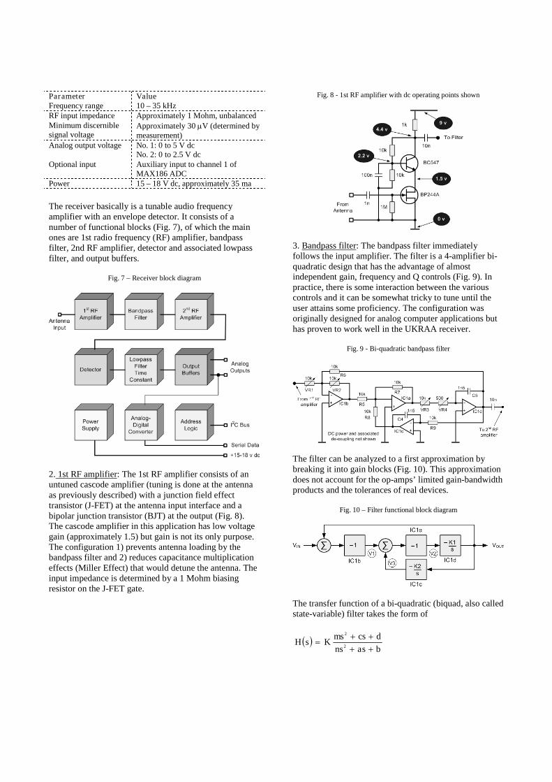
2. 1st RF amplifier: The 1st RF amplifier consists of anuntuned cascode amplifier (tuning is done at the antennaas previously described) with a junction field effecttransistor (J-FET) at the antenna input interface and abipolar junction transistor (BJT) at the output (Fig. 8).The cascode amplifier in this application has low voltagegain (approximately 1.5) but gain is not its only purpose.The configuration 1) prevents antenna loading by thebandpass filter and 2) reduces capacitance multiplicationeffects (Miller Effect) that would detune the antenna. Theinput impedance is determined by a 1 Mohm biasingresistor on the J-FET gate.
Fig. 8 - 1st RF amplifier with dc operating points shown
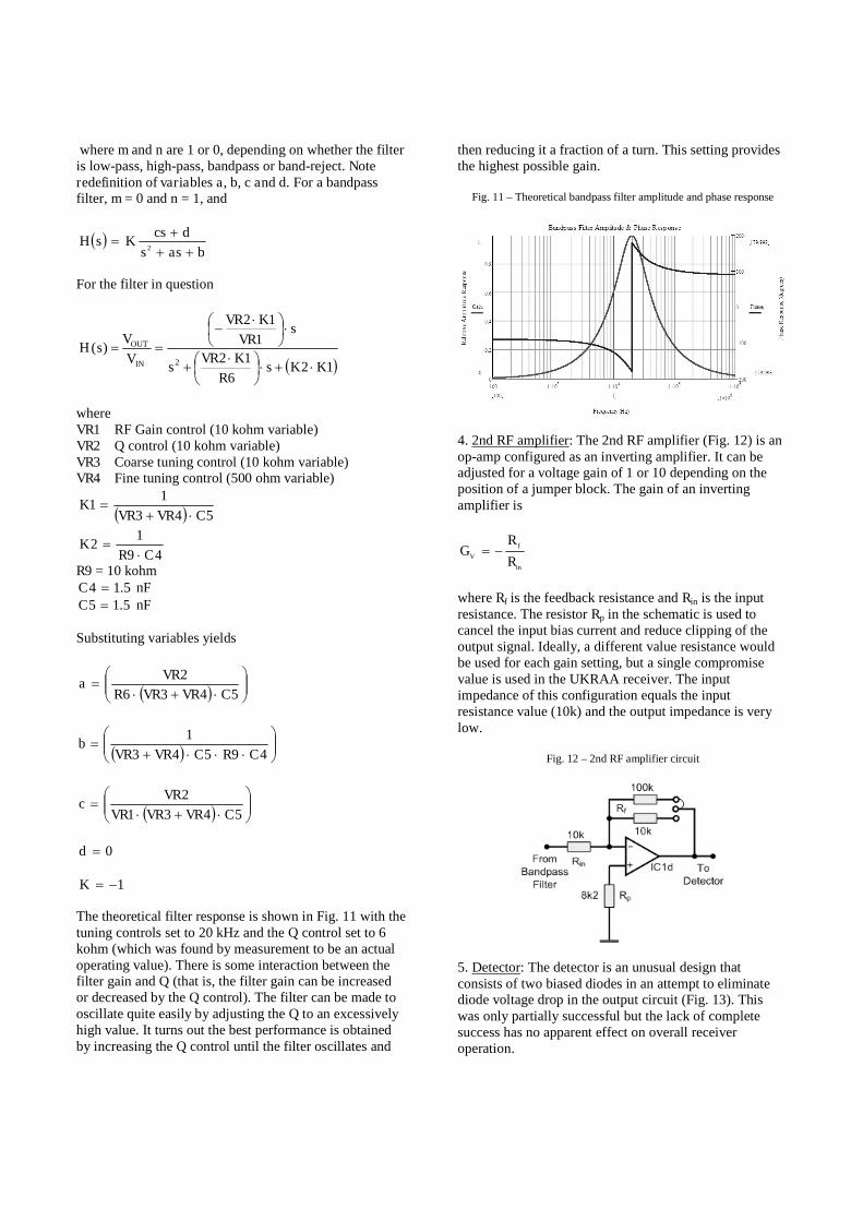
3. Bandpass filter: The bandpass filter immediatelyfollows the input amplifier. The filter is a 4-amplifier bi-quadratic design that has the advantage of almostindependent gain, frequency and Q controls (Fig. 9). Inpractice, there is some interaction between the variouscontrols and it can be somewhat tricky to tune until theuser attains some proficiency. The configuration wasoriginally designed for analog computer applications buthas proven to work well in the UKRAA receiver.
Fig. 9 - Bi-quadratic bandpass filter
The filter can be analyzed to a first approximation bybreaking it into gain blocks (Fig. 10). This approximationdoes not account for the op-amps’ limited gain-bandwidthproducts and the tolerances of real devices.
Fig. 10 – Filter functional block diagram
The transfer function of a bi-quadratic (biquad, also calledstate-variable) filter takes the form of
basns
dcsmsKsH
2
2
where m and n are 1 or 0, depending on whether the filteris low-pass, high-pass, bandpass or band-reject. Noteredefinition of variables a, b, c and d. For a bandpassfilter, m = 0 and n = 1, and
bass
dcsKsH
2
For the filter in question
126
12
1
12
)(2 KKs
R
KVRs
sVR
KVR
V
VsH
IN
OUT
whereVR1 RF Gain control (10 kohm variable)VR2 Q control (10 kohm variable)VR3 Coarse tuning control (10 kohm variable)VR4 Fine tuning control (500 ohm variable)
543
11
CVRVRK
49
12
CRK
R9 = 10 kohm5.14 C nF
5.15 C nF
Substituting variables yields
5436
2
CVRVRR
VRa
49543
1
CRCVRVRb
5431
2
CVRVRVR
VRc
0d
1K
The theoretical filter response is shown in Fig. 11 with thetuning controls set to 20 kHz and the Q control set to 6kohm (which was found by measurement to be an actualoperating value). There is some interaction between thefilter gain and Q (that is, the filter gain can be increasedor decreased by the Q control). The filter can be made tooscillate quite easily by adjusting the Q to an excessivelyhigh value. It turns out the best performance is obtainedby increasing the Q control until the filter oscillates and
then reducing it a fraction of a turn. This setting providesthe highest possible gain.
Fig. 11 – Theoretical bandpass filter amplitude and phase response
4. 2nd RF amplifier: The 2nd RF amplifier (Fig. 12) is anop-amp configured as an inverting amplifier. It can beadjusted for a voltage gain of 1 or 10 depending on theposition of a jumper block. The gain of an invertingamplifier is
in
f
VR
RG
where Rf is the feedback resistance and Rin is the inputresistance. The resistor Rp in the schematic is used tocancel the input bias current and reduce clipping of theoutput signal. Ideally, a different value resistance wouldbe used for each gain setting, but a single compromisevalue is used in the UKRAA receiver. The inputimpedance of this configuration equals the inputresistance value (10k) and the output impedance is verylow.
Fig. 12 – 2nd RF amplifier circuit
5. Detector: The detector is an unusual design thatconsists of two biased diodes in an attempt to eliminatediode voltage drop in the output circuit (Fig. 13). Thiswas only partially successful but the lack of completesuccess has no apparent effect on overall receiveroperation.

Fig. 13 – Detector and lowpass filter circuit
The detector output is filtered by two resistance-capacitance (RC) circuits, with time constants of 100seconds and 1 second, respectively. The detector filterprovides a fast rise-time (1 -2 seconds) and very slow falltime (30-40 seconds). This helps to smooth the outputwhen there are noise and quickly changing propagationconditions but provides good response to SID events. Avoltage limiter circuit (not shown in the schematic above)is connected across the detector output to keep fromoverdriving the output buffers with strong noise or signallevels.
6. Output buffers: The receiver has two output buffers,one with a fixed voltage gain of 2 for 0 to 5 V analogoutput. The other buffer can be set by resistor placementfor a voltage gain of 1 or 2 for 0 to 2.5 V or 0 to 5 Voutput. These two ranges accommodate almost alldataloggers.
The output buffers are configured as non-invertingamplifiers (Fig. 14). The gain of a non-inverting amplifieris
1
1R
RG
f
V
where Rf is the feedback resistance and R1 is the resistancefrom the inverting input to ground. The input impedanceof this configuration is very high and the outputimpedance is very low.
Fig. 14 – Output buffer (typical of two)
7. On-board options: The printed circuit board (PCB) hasprovisions for a MAX186 analog-digital converter IC thatcan be connected to a PC parallel printer port and usedwith Radio-SkyPipe software. The setup includes optionjumpers for selecting the PCB output connector and alsofor connecting an auxiliary input port to an unusedchannel on the ADC.
The PCB includes a temperature sensor that uses the I2Cbus for connection to a compatible controller. The PCBalso has an electrically erasable programmable read-onlymemory (EEPROM) IC for setting the receiver addressand storing configuration attributes when the receiver isused with a controller and Starbase software. Thesefunctions allow the receiver and other planned andexisting UKRAA projects to work as a remotely or locallycontrolled unified observatory.
III. RECEIVER KIT CONSTRUCTION
1. Kit contents: The kit includes a silkscreened 2-sidedPCB and all on-board components (Fig. 15). There areapproximately 80 components and all are through-holetypes except one (the LM73 temperature sensor is asurface-mounted device, SMD, and it is pre-soldered tothe PCB).
Fig. 15 – Printed circuit board ready for assembly. Dimensions are 114mm x 100 mm
The kit includes only the PCB-mounted parts. Externalparts such as enclosure, antenna connector, dc power jackand output connectors are not provided. This allowsbuilders to put the PCB in an enclosure of choice and useinterface parts that are on-hand or meet their particularrequirements.
2. Construction: There were no surprises during assemblyand testing. The receiver assembly manual has enoughdetail for anyone with technical aptitude and minimumsoldering skills. UKRAA provides a separate user manual

that includes tuning and application information. Manualsmay be downloaded from www.ukraa.com/vlfkit.
The receiver design is simple enough that few problemswill be encountered beyond poor soldering or incorrectcomponent placement. The completed board is notcrowded and solder landings are properly sized for a fine-tip soldering iron (Fig. 16).
Fig. 16 – Completed receiver PCB ready for testing
Two receivers were assembled. One was placed in arecycled computer/printer I/O switch box and the other ina new aluminum enclosure (Fig. 17). The receiver shouldbe installed in a metal (and not plastic) enclosure tominimize electromagnetic interference (EMI). Thereceiver PCB dimensions are compatible with theHammond Mfg. p/n 1455N1601 extruded aluminumenclosure.
Both receiver enclosures were equipped with 3.5 mmphone jacks for input tuning and analog outputs and asmall analog voltmeter for monitoring and tuning. Also,both receivers were converted to 12 V dc operation(rather than 15 V) by replacing the voltage regulator IC.One receiver was equipped with a 2-stage J-FETpreamplifier and associated bypass switch forexperimental purposes.
Fig. 17 – Completed receivers. Dimensions (a) upper three pictures: 150mm x 135 mm x 60 mm, (b) lower three pictures: 115 mm x 180 mm x55 mm. Receiver (a) has an experimental 2-stage preamplifier (seen on
the right of the middle photograph)
(a)
(b)
IV. PERFORMANCE

1. Receiving conditions in Alaska: Considerable difficultyhas been encountered in Anchorage, Alaska with reliablyreceiving VLF transmissions, apparently due to persistentlocal interference, distance from transmitter stations andpossible propagation conditions at northern latitudes. Alltests were performed indoors during the winter of2009/2010 with no opportunity to move the antennaoutdoors and away from potential interference sources.The same problem was encountered with other receiverdesigns including the SolarSID and SuperSID as well as aparticularly interesting setup using a frequency selectivelevel meter as a receiver (Rycom model 6020). A limitedamount of data was obtained with the UKRAA VLFreceiver but there were no solar flares during this period(Fig. 18).
Fig. 18 – UKRAA VLF receiver outputs during late November 2009
There are four known VLF transmitter stations in the USthat operate in the UKRAA receiver’s frequency range(Fig. 19). The closest transmitter to Anchorage, Alaska isNLK (24.8 kHz) in Washington, a distance of about 2,300km. The distances are large enough that groundwavereception probably is out of the question, and spacewavesvia the Earth-ionosphere waveguide mode may beconsiderably attenuated while traveling multiple hops.The 4,600 km path from Lualualei, Hawaii (NPM at 21.4
kHz) to Anchorage is entirely over water and may providea good multi-path opportunity because of the lowerattenuation on this type of path. The other paths areoverland.
Fig. 19 – VLF transmitting stations with respect to Anchorage, Alaska(Underlying map source: www.wm7d.net/az_proj/az_html)
2. Improving performance: Where the distance betweenthe transmitter and UKRAA receiver exceeds around1,000 km, a larger antenna may be advisable. The existingsquare loop design can be scaled up to any practicaldimension or other shapes can be used. Attention willneed to be paid to the self-resonant frequency due todistributed capacitance of the windings.
There is plenty of room for experimentation with thereceiver design to improve its performance. Someexamples are 1) slight redesign of the 1st RF inputamplifier to increase its gain, 2) addition of a preamplifierwith balanced low impedance input and unbalanced highimpedance output to better match antenna to 1st RFamplifier, 3) replacement of the inexpensive TL084 ICused in IC1 (bandpass filter) with a higher performancequad op-amp, 4) tweaking of the bandpass filter circuit toreduce the chance of oscillation at high Q settings, and 5)shielding between stages to reduce undesired feedback.
V. CONCLUSIONS
The UKRAA VLF Receiver System consists of a loopantenna, antenna tuning unit and receiver. The receiverdesign is unique among units used by amateur radioastronomers and has been used with considerable success

in the UK and Europe. The antenna and receiver inputcircuits are designed for receiving conditions in thatregion, where suitable VLF transmitters are less than1,000 km away. The receiver should work well in muchof the US, as well, although considerable difficulty hasbeen encountered in Alaska reliably receiving stations, theclosest of which is 2,300 km away. It may be necessary touse a larger antenna in some locations.
References
[1] Coyle, L., A Modular Receiver for Exploring theLF/VLF Bands, QST, Part 1: Nov 2008, Part 2: Dec2008
[2] Stokes, A., A Gyrator Tuned VLF Receiver,Communications Quarterly, Spring 1994
[3] Stokes, A., Gyrator II - An Improved Gyrator TunedVLF Receiver, American Association of VariableStar Observers - Solar Division, Vol. 10, No. 1, Jul1999
[4] Gentges, F & Ratzlaff, S., AMRAD Low FrequencyUpconverter, QST, Apr 2002
[5] Stanford Solar Center, SID Monitors at: http://solar-center.stanford.edu/SID/
Acknowledgements
The following UKRAA members patiently answered aconsiderable number of questions about the receiverdesign and application: John Cook, Andrew Lutley, AlanMelia, Laurence Newell, and Norman Pomfret.
Author Information
Whitham Reeve was born in Anchorage,Alaska and has lived there his entire life.He became interested in electronics in1958 and worked in the airline industry inthe 1960s and 1970s as an avionicstechnician, engineer and managerresponsible for the design, installation andmaintenance of electronic equipment andsystems in large airplanes. For the next 37years he worked as an engineer in the
telecommunications and electric utility industries with the last32 years as owner and operator of Reeve Engineers, anAnchorage-based consulting engineering firm. Mr. Reeve is aregistered professional electrical engineer with BSEE and MEEdegrees. He has written a number of books for practicingengineers and enjoys writing about technical subjects. Recentlyhe has been building a radio science observatory for studyingelectromagnetic phenomena associated with the Sun, Earth andother planets.
© 2010 Whitham D. Reeve