Embed Size (px)
Citation preview
Journal of Applied Research and Technology 211
Application of nonlinear compensation to limit input dynamic range in analog optical fiber links J. Rodriguez*1, J. Velazquez2, R. Garduno3, J. Montero4 1,2,3,4 Instituto de Investigaciones Electricas, Control and Instrumentation Department Reforma 113, Col. Palmira, 62490 Cuernavaca, Morelos, Mexico *[email protected] ABSTRACT The dynamic range of a signal at the input of a measurement system during a short circuit test is increased several times by the nominal input voltage. Saturation of the measurement system may occur in a device under failure test. This paper introduces the application of a nonlinear compensation to limit the voltage range at the input of a voltage controlled oscillator which is used to produce the pulsed frequency modulation needed to transmit the analog signals over the optical fiber links. The proposed dynamic range compensation system is based on non-linear circuits to accommodate the input range of the voltage controlled oscillator. This approach increases the transient signal handling capabilities of the measuring system. This work demonstrates that the nonlinear compensated optical fiber approach yields a unique, electrically isolated, lightning-proof analog data transmission system for remote measuring systems in the highly aggressive EMI environment of high-power test laboratories. Keywords: Nonlinear compensation, VCO dynamic input range, EMI, high power testing, optical fiber link. RESUMEN Cuando un dispositivo bajo prueba falla durante una prueba de corto circuito, la señal esperada se incrementa y la saturación de voltaje a la entrada del sistema de medición dificulta el análisis de la falla. Este artículo introduce la aplicación de una compensación no lineal para limitar el rango de voltaje en la entrada de un oscilador controlado por voltaje, el cual es usado para producir la modulación pulsada en frecuencia necesaria para transmitir las señales analógicas sobre las cadenas de fibra óptica. El sistema de compensación dinámica de rango propuesto está basado en circuitos no lineales para acomodar el rango de entrada del oscilador controlado por voltaje. Este enfoque incrementa la capacidad de manejo de señales del sistema de medición. Este trabajo demuestra que las cadenas de fibra óptica compensadas no linealmente proporciona un sistema de transmisión de datos analógicos único, eléctricamente aislado y a prueba de descargas eléctricas para sistemas de medición remotos en el ambiente altamente agresivo de un laboratorio de pruebas de alta potencia. 1. Introduction Optical fibers have been mainly used in digital communication applications, for which high speed and large bandwidth are major requirements whereas transmission of a DC component is not necessary. On the other hand, the accuracy and precision of analog optical fiber transmission links for a measuring system, subject to very aggressive EMI conditions and other transient phenomena, is highly dependent on maintaining under control the DC voltage offset drift due to temperature change. Consequently, it is highly desirable to devise and to implement a compensation mechanism to satisfy the measuring system requirements and to be able to handle large dynamic voltage changes.
On the other hand, companding is a signal processing technique primarily used in audio digital systems such as microphones and wireless communications to reduce noise levels. The objective of the companding process is to preserve the signal-to-noise ratio of the original audio signal. Non-linear compensation functions are mainly used in voice communication companding. The non-linear µ-law algorithm is used for companding in the digital telecommunication systems of North America and Japan, while the non-linear A-law algorithm is used in Europe [1]. The use of companding for analog picture transmission was patented by A. B. Clark of AT&T in 1928 [2]. Also in 1942, Clark and his team completed the secure voice transmission system, which was the first application of companding in a PCM system.[3].

Application of nonlinear compensation to limit input dynamic range in analog optical fiber links, J. Rodriguez et al., 211‐226
Vol.8 No.2 August 2010 212
Then in 1953, B. Smith showed that a nonlinear DAC could simplify the design of digital companding systems [4]. In 1965, R. Dolby in Britain developed a simple compander known as the Dolby Noise Reduction System. One of the features that set Dolby's compander apart was that it took care only of the quiet sounds that otherwise would be masked by tape noise. Dolby marketed the product to record companies. In 1970, H. Kaneko developed the uniform description of segment (piecewise linear) companding laws that have been adopted in digital telephony [5].
Digital techniques of radio over fiber (RoF) communications can be deployed with optical fibers. The measuring system in this work uses the simplest RoF method for optical transmission by Direct Intensity Modulation. This method falls under the Intensity Modulation – Direct Detection (IM-DD) technique [6]. The direct Intensity Modulation used to implement PFM optical fiber link is the metod that complies with the requirement to transmit DC components. Table I shows a comparison of the available techniques for optical fiber links, applicable to measurement systems.
Features Nicolet Isobe 5500 Teseo OAM01 Our Solution Bandwith -3dB DC to 20 MHz DC to 1MHz DC to 1 MHz Flat zone DC to 1 MHz 5% +/- 1.5 dB DC to 200 kHz 1%SNR -60 dB rms > 50 dB > 50 dB Input impedance 1 MOhm 47pF 1 MOhm 1 MOhm Input range ± 100 mV to ±50 V in
1,2,5 steps ±0.51/2.5/5/10/25/ 50/100/250 V
200 mV to 600 V in 7 steps
Output impedance
50 Ohms 50 Ohms 50 Ohms
DC gain drift <2.5 mV por °C in Rx <2.0 mV /°C in Tx Operation temperature
0 a 45 °C -10 to70 °C in Tx 0 to 50 °C in Rx
0 to 50 °C
Fiber Optic connector
SMA ST signal and control
ST signal and control
Battery duration 4 Hrs with internal charger 8 Hrs with external charger
>8 hrs >6 hrs
Power 160 mA, 125 V N/A 200 mA
Table 1. Comparison of optical fiber links.
Application of nonlinear compensation to limit input dynamic range in analog optical fiber links, J. Rodriguez et al., 211‐226
Journal of Applied Research and Technology 213
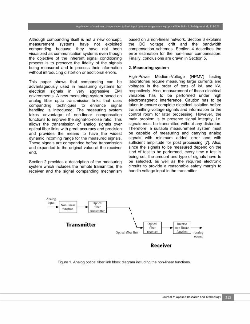
Although companding itself is not a new concept, measurement systems have not exploited companding because they have not been visualized as communication systems even though the objective of the inherent signal conditioning process is to preserve the fidelity of the signals being measured and to process their information without introducing distortion or additional errors. This paper shows that companding can be advantageously used in measuring systems for electrical signals in very aggressive EMI environments. A new measuring system based on analog fiber optic transmission links that uses companding techniques to enhance signal handling is introduced. The measuring system takes advantage of non-linear compensation functions to improve the signal-to-noise ratio. This allows the transmission of analog signals over optical fiber links with great accuracy and precision and provides the means to have the widest dynamic incoming range for the measured signals. These signals are companded before transmission and expanded to the original value at the receiver end. Section 2 provides a description of the measuring system which includes the remote transmitter, the receiver and the signal companding mechanism
based on a non-linear network. Section 3 explains the DC voltage drift and the bandwidth compensation schemes. Section 4 describes the error estimation for the non-linear compensation. Finally, conclusions are drawn in Section 5. 2. Measuring system High-Power Medium-Voltage (HPMV) testing laboratories require measuring large currents and voltages in the order of tens of kA and kV, respectively. Also, measurement of these electrical variables has to be performed under high electromagnetic interference. Caution has to be taken to ensure complete electrical isolation before transmitting voltage signals and information to the control room for later processing. However, the main problem is to preserve signal integrity, i.e. signals must be transmitted without any distortion. Therefore, a suitable measurement system must be capable of measuring and carrying analog signals with minimum added error and with sufficient amplitude for post processing [7]. Also, since the signals to be measured depend on the kind of test to be performed, every time a test is being set, the amount and type of signals have to be selected, as well as the required electronic circuits to provide a reasonable safety margin to handle voltage input in the transmitter.
Figure 1. Analog optical fiber link block diagram including the non-linear functions.

Application of nonlinear compensation to limit input dynamic range in analog optical fiber links, J. Rodriguez et al., 211‐226
Vol.8 No.2 August 2010 214
The analog fiber optic link of the measuring system is basically a fiber optic transceiver composed by three major components which include the remote transmitter, the receiver unit and the fiber optic communication link, as shown in Figure 1. The remote transmitter, located in the high EMI testing area at the HPMT laboratory, performs the measurements, sets up and sends out the analog input signal. The receiver unit, located in the control room at the HPMT laboratory, demodulates and filters the transmitted signal and drives the resultant analog output forward for digitizing and further processing. The communication link consists of two optical fiber channels that provide electrical isolation and immunity to the high voltage and EMI in the HPMT laboratory environment. The analog fiber optic link was designed to accomplish a flat-zone bandwidth from DC through 200 KHz, with 5 mV/°C maximum DC shifting and no more than 1% gain variation through the link. Due to the wide range of the analog input voltages, the remote transmitter has a conditioning front-end that can manage signals from 200 mV to 200 V in nine selectable attenuation ranges. A non-linear network, which implements a non-linear mathematical function, is used to ensure that the optimum input voltage for the modulator is not exceeded. Once in the remote transmitter, the analog input signal is modulated in frequency and converted into an infrared light ray to travel along the optical fiber channel. At the other channel end, the receiver is in charge of converting back the signal from light to voltage, amplifying, demodulating and conditioning it so it can be used
for post processing. The analog output signal is fed into a non-linear network that implements the inverse mathematical function used for companding in the transmitter. The final output voltage is in the ±10 V range and can be acquired and processed by an analog to digital converter (ADC). Configurable features allow selection of input range for operation, diagnosis and automatic self-calibration. Also, the versatile power supply inside the transmitter can detect AC power supply or switch to batteries if AC power is not available. An internal digital remote controller senses battery voltage and controls battery charge. A. Remote transmitter The transmitter equipment consists of both digital and analog sections, which are physically separated but interact with one another. The digital section is in charge of receiving and interpreting the serial commands upcoming from the digital section of the receiver equipment in the control room. The analog section performs signal conditioning. Then, the signal is Pulsed Frequency Modulated (PFM) and converted into an infrared light signal in order to be transported through the optical fiber channel. As depicted in Figure 2, five modules integrate the remote transmitter: digital remote controller, analog conditioning module, non-linear networks, analog transmitter and power supply. One fiber optic link is used to receive control commands and the other is multiplexed for control command reply and analog signal transmission.
a)

Application of nonlinear compensation to limit input dynamic range in analog optical fiber links, J. Rodriguez et al., 211‐226
Journal of Applied Research and Technology 215
The central element of the analog transmitter is a VCO (voltage controlled oscillator) that oscillates at some initial frequency in accordance to a voltage setpoint VS to generate the output of the VCO at frequency ω0, called the central free-running frequency. The output frequency of the VCO is
( ) ( )0 VCO Et G V tω ω= + (1) where GVCO is the VCO voltage-to-radian frequency gain in radians per second per volt and VE is the applied voltage to the control input of the VCO to set the central angular frequency and to modulate ω(t). The input voltage is
( ) ( )E m S NV t V t V V= + + (2)
where Vm(t) is the modulating signal, VS is the DC setpoint voltage to produce ω0 and VN is the noise voltage at the input of the VCO. Substitution of (2) into (1) yields
( ) ( )( )0 VCO m S Nt G V t V Vω ω= + + + (3)
On the other hand, the VCO can be expressed as
( ) ( )( )0sinCO AMPL VC E OFFV t V t G V t dt Vω= + +∫ (4)
The nonlinear function is based on the I–V characteristic of two diodes in parallel configuration to have symmetric current for positive and negative
imput signal voltage. The equation of an ideal diode is
( )( )1D TV nVSI I e= − (5)
Where I is the diode current, Is is a scale factor called the saturation current, VD is the voltage across the diode, VT is the thermal voltage, and n is the emission coefficient, also known as the ideality factor. The emission coefficient n varies from about 1 to 2 depending on the fabrication process and semiconductor material and, in many cases, is assumed to be approximately equal to 1 (thus the notation n is omitted). The thermal voltage VT is approximately 25.85 mV at 300 K, a temperature close to “room temperature” commonly used in device simulation software. At any temperature it is a known constant defined by
TkTVq
= (6)
Where q is the magnitude of charge on an electron (the elementary charge), k is Boltzmann’s constant, T is the absolute temperature of the p-n junction in Kelvin degrees. At reverse bias voltages, the exponential in the diode equation is negligible, and the current is a constant (negative) reverse current value of -IS. For even smaller forward bias voltages, the exponential is very large because the thermal voltage is very small, so the subtracted ‘1’ in the diode equation is negligible and the forward diode current is often approximated as
Figure 2. a) Transmitter block diagram. b) Actual implementation of the Transmitter Non-linear network.
b)

Application of nonlinear compensation to limit input dynamic range in analog optical fiber links, J. Rodriguez et al., 211‐226
Vol.8 No.2 August 2010 216
( )D TV nVSI I e= (7)
The current for a diode network of two diodes in parallel, one forward and one backwards is
( ) ( )sgn D TV nVD SI V I e= (8)
This diode equation is used to limit the voltage range of a bipolar signal at the input of the modulator, and the inverse function to reconstruct the original shape of the input voltage at the receiver. The output voltage for the transmitter is
( )sgn ln inout in T
S
vv v nV
I R⎛ ⎞
= − ⎜ ⎟⎝ ⎠
(9)
The output voltage (inverse function) for the receiver is
( ) ( )sgn D TV nVout D Sv V RI e= (10)
B. Receiver The receiver equipment is available in a rack-mount configuration. Up to 32 receiver channels can be plugged in one rack enclosure to ease connection to the rack-mounted data acquisition system in the control room. As with the transmitter equipment, the receiver also has both analog and digital sections. Figure 3 shows a simplified block diagram of one receiver. The analog section is in charge of detecting, amplifying and demodulating the incoming PFM signal from the transmitter module, the demodulated signal is introduced to the inverse nonlinear function network to recover the original signal from the transmitter. And the output level is adjusted for digitization and post-processing. The digital section is the interface between the remote control system and the remote transmitter; it is responsible for sending and receiving commands trough an RS-485 interface.
Figure 3. a). Receiver block diagram b). Current implementation of the
receiver non-linear network inverse function.
Application of nonlinear compensation to limit input dynamic range in analog optical fiber links, J. Rodriguez et al., 211‐226
Journal of Applied Research and Technology 217
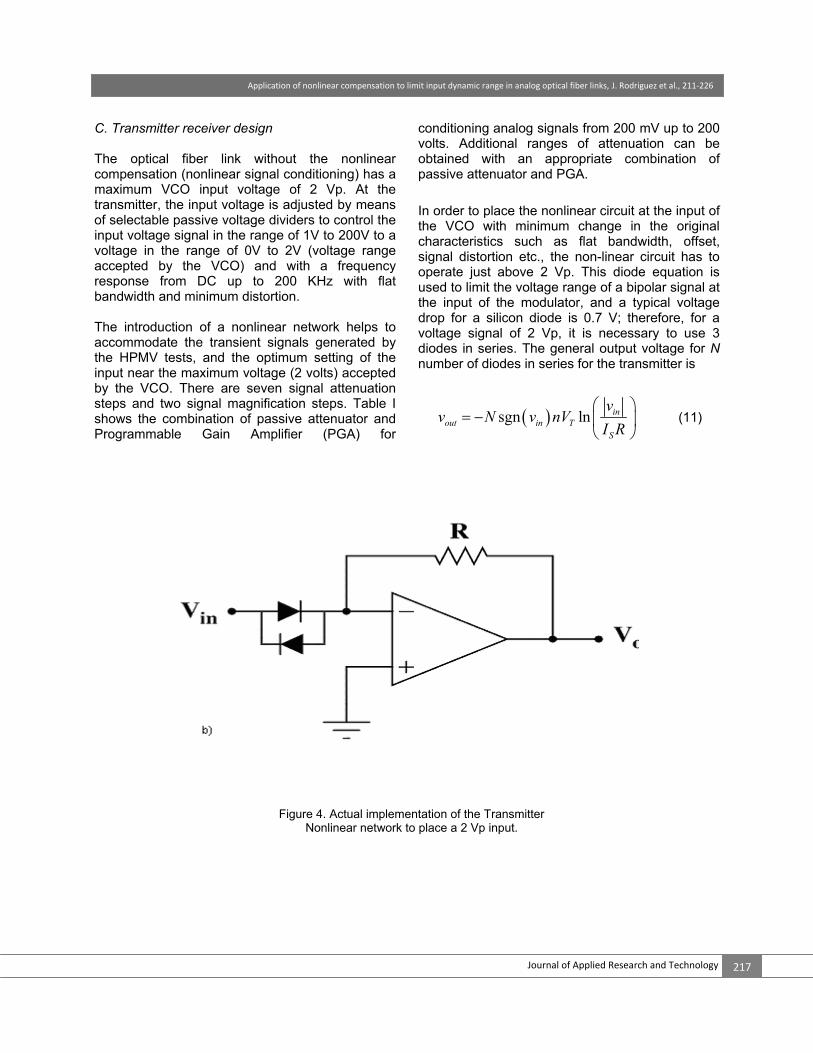
C. Transmitter receiver design The optical fiber link without the nonlinear compensation (nonlinear signal conditioning) has a maximum VCO input voltage of 2 Vp. At the transmitter, the input voltage is adjusted by means of selectable passive voltage dividers to control the input voltage signal in the range of 1V to 200V to a voltage in the range of 0V to 2V (voltage range accepted by the VCO) and with a frequency response from DC up to 200 KHz with flat bandwidth and minimum distortion. The introduction of a nonlinear network helps to accommodate the transient signals generated by the HPMV tests, and the optimum setting of the input near the maximum voltage (2 volts) accepted by the VCO. There are seven signal attenuation steps and two signal magnification steps. Table I shows the combination of passive attenuator and Programmable Gain Amplifier (PGA) for
conditioning analog signals from 200 mV up to 200 volts. Additional ranges of attenuation can be obtained with an appropriate combination of passive attenuator and PGA. In order to place the nonlinear circuit at the input of the VCO with minimum change in the original characteristics such as flat bandwidth, offset, signal distortion etc., the non-linear circuit has to operate just above 2 Vp. This diode equation is used to limit the voltage range of a bipolar signal at the input of the modulator, and a typical voltage drop for a silicon diode is 0.7 V; therefore, for a voltage signal of 2 Vp, it is necessary to use 3 diodes in series. The general output voltage for N number of diodes in series for the transmitter is
( )sgn ln inout in T
S
vv N v nV
I R⎛ ⎞
= − ⎜ ⎟⎝ ⎠
(11)
Figure 4. Actual implementation of the Transmitter Nonlinear network to place a 2 Vp input.

Application of nonlinear compensation to limit input dynamic range in analog optical fiber links, J. Rodriguez et al., 211‐226
Vol.8 No.2 August 2010 218
Figure 5. Calculated nonlinear curves for the transmitter at the input of the VCO for small signal silicon diodes in series in accordance with Figure 4.
Figure 6. Current implementation of the receiver nonlinear network inverse function.
Application of nonlinear compensation to limit input dynamic range in analog optical fiber links, J. Rodriguez et al., 211‐226
Journal of Applied Research and Technology 219
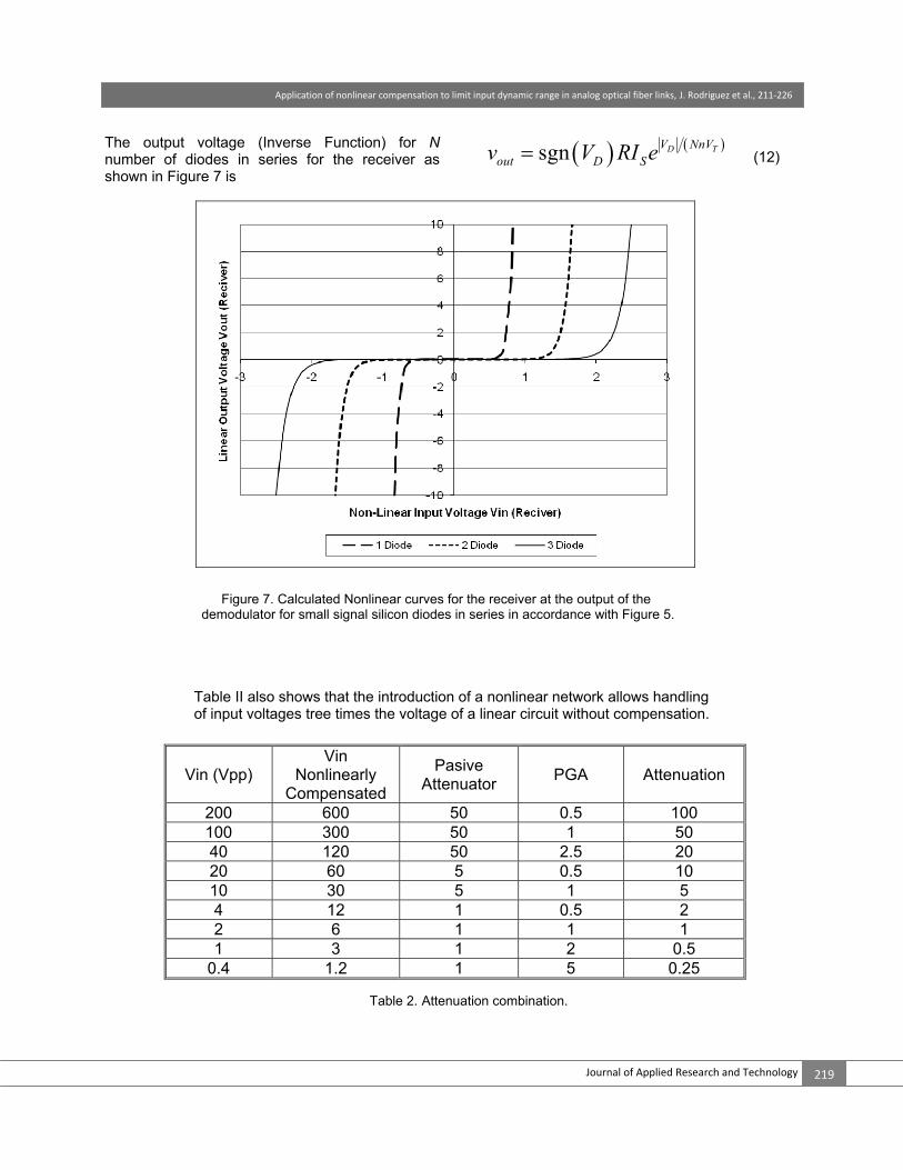
The output voltage (Inverse Function) for N number of diodes in series for the receiver as shown in Figure 7 is
( ) ( )sgn D TV NnVout D Sv V RI e= (12)
Figure 7. Calculated Nonlinear curves for the receiver at the output of the demodulator for small signal silicon diodes in series in accordance with Figure 5.
Vin (Vpp) Vin
Nonlinearly Compensated
Pasive Attenuator PGA Attenuation
200 600 50 0.5 100 100 300 50 1 50 40 120 50 2.5 20 20 60 5 0.5 10 10 30 5 1 5 4 12 1 0.5 2 2 6 1 1 1 1 3 1 2 0.5
0.4 1.2 1 5 0.25
Table 2. Attenuation combination.
Table II also shows that the introduction of a nonlinear network allows handling of input voltages tree times the voltage of a linear circuit without compensation.
Application of nonlinear compensation to limit input dynamic range in analog optical fiber links, J. Rodriguez et al., 211‐226
Vol.8 No.2 August 2010 220
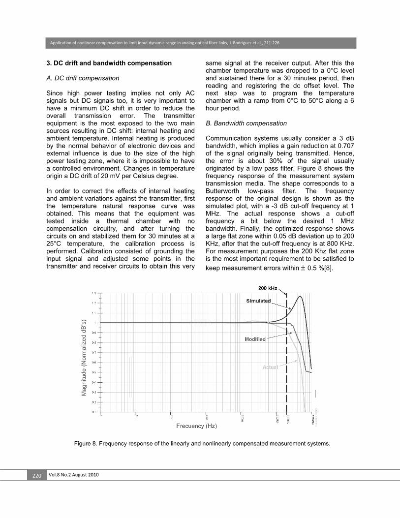
3. DC drift and bandwidth compensation A. DC drift compensation Since high power testing implies not only AC signals but DC signals too, it is very important to have a minimum DC shift in order to reduce the overall transmission error. The transmitter equipment is the most exposed to the two main sources resulting in DC shift: internal heating and ambient temperature. Internal heating is produced by the normal behavior of electronic devices and external influence is due to the size of the high power testing zone, where it is impossible to have a controlled environment. Changes in temperature origin a DC drift of 20 mV per Celsius degree. In order to correct the effects of internal heating and ambient variations against the transmitter, first the temperature natural response curve was obtained. This means that the equipment was tested inside a thermal chamber with no compensation circuitry, and after turning the circuits on and stabilized them for 30 minutes at a 25°C temperature, the calibration process is performed. Calibration consisted of grounding the input signal and adjusted some points in the transmitter and receiver circuits to obtain this very
same signal at the receiver output. After this the chamber temperature was dropped to a 0°C level and sustained there for a 30 minutes period, then reading and registering the dc offset level. The next step was to program the temperature chamber with a ramp from 0°C to 50°C along a 6 hour period. B. Bandwidth compensation Communication systems usually consider a 3 dB bandwidth, which implies a gain reduction at 0.707 of the signal originally being transmitted. Hence, the error is about 30% of the signal usually originated by a low pass filter. Figure 8 shows the frequency response of the measurement system transmission media. The shape corresponds to a Butterworth low-pass filter. The frequency response of the original design is shown as the simulated plot, with a -3 dB cut-off frequency at 1 MHz. The actual response shows a cut-off frequency a bit below the desired 1 MHz bandwidth. Finally, the optimized response shows a large flat zone within 0.05 dB deviation up to 200 KHz, after that the cut-off frequency is at 800 KHz. For measurement purposes the 200 Khz flat zone is the most important requirement to be satisfied to keep measurement errors within ± 0.5 %[8].
Figure 8. Frequency response of the linearly and nonlinearly compensated measurement systems.

Application of nonlinear compensation to limit input dynamic range in analog optical fiber links, J. Rodriguez et al., 211‐226
Journal of Applied Research and Technology 221
The whole fiber optic analog link can be simply modeled with the second order transfer function:
( )13
2 6 12
1.984 104.084 10 9.87 10
G ss s
×=
+ × + × (13)
which has the following main properties: DC gain Gdc=2.01, peak gain Gp=2.02, natural oscillation frequency fn= 500 kHz, damping coefficient ζ=0.65, and time constant τ =0.489 μs. To illustrate the time domain performance of the nonlinearly compensated measurement system,
Figure 9 shows a triangular continuous wave as input voltage, the squared wave is the nonlinear output and the dotted triangular wave is the reconstructed signal at the receiver. The measurement system has a gain of Vo/Vi=2. Results show that the use of nonlinear networks improves the dynamic range of the input voltage at the transmitter and is able to reconstruct the original signal maintaining original bandwidth and low distortion. Figure 10 shows a simulated current signal during a short-circuit test of the nonlinearly compensated measurement system.
Figure 9. Input vs. output time response of the nonlinearly compensated measurement system.

Application of nonlinear compensation to limit input dynamic range in analog optical fiber links, J. Rodriguez et al., 211‐226
Vol.8 No.2 August 2010 222
4. Error estimation for the nonlinear compensation Accuracy and precision are measured and estimated for the transmitter, the receiver and for the complete optical fiber link measuring system. Accuracy is determined by systematic errors and limited by precision. Precision is determined by random errors. Sources of systematic error are linearity deviation, frequency response, voltage offset, signal gain and optical power regulation for the optical link. Sources of random error are thermal voltage offset drift, modulator-demodulator thermal voltage offset drift, modulator-demodulator thermal voltage gain drift, thermal noise, power supply noise. Thermal Voltage offset and thermal voltage gain drift of the modulator is locally compensated to limit the error. Thermal voltage offset and thermal voltage gain drift of the demodulator is compensated by maintaining the temperature constant in the control room at 20 ºC.
The overall accuracy of the measurement system was measured and was smaller than 1%.
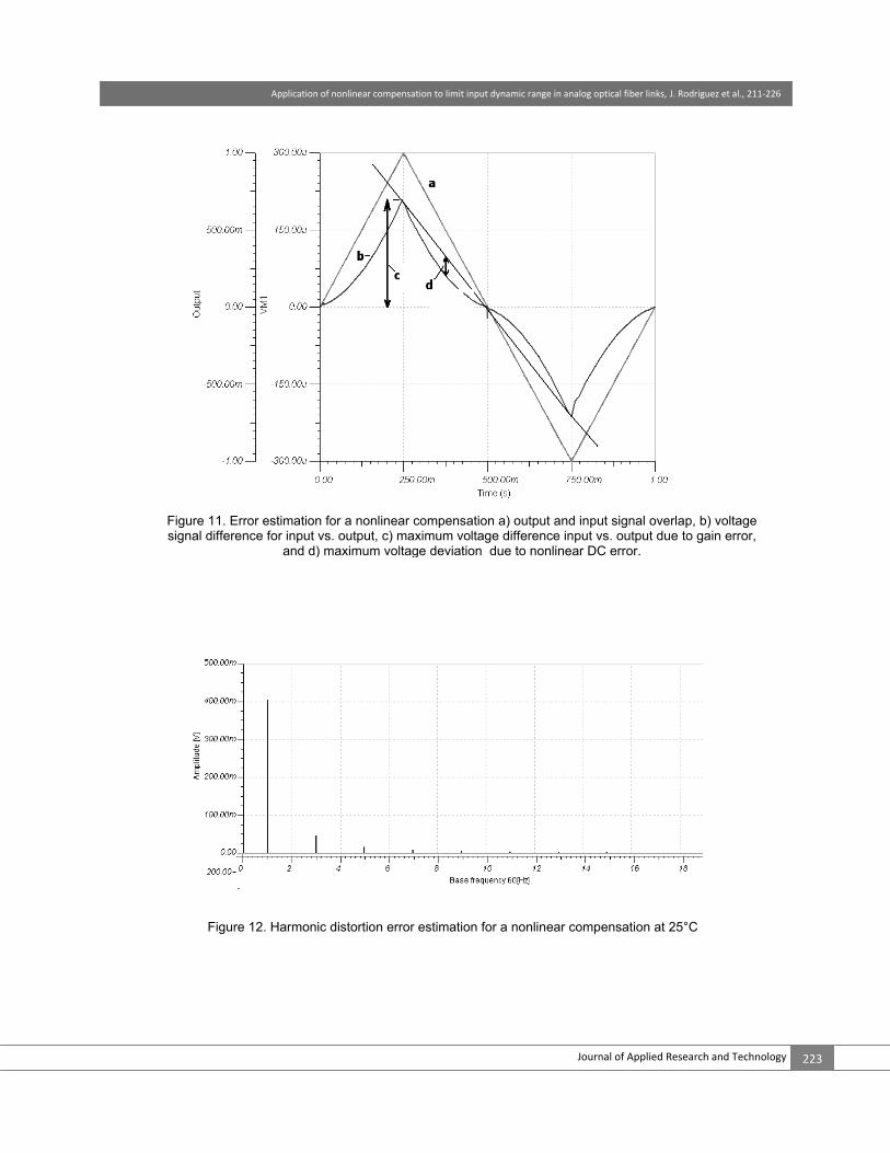
The introduction of a nonlinear compensation requires the consideration of errors related to gain, DC nonlinearity and AC distortion caused by the nonlinearity. Figure 11 shows the input-output signals and the difference to estimate the error introduced by a nonlinear compensation, a one-volt signal is applied to the input, and the output voltage overlaps with the input; the voltage signal difference for input vs. output helps to determine the gain and nonlinearity errors. The gain error is approximately 0.2 %, and the nonlinearity error is approximately 0.03 % for a transmitter and receiver operating at the same temperature. Figure 12 shows the harmonic distortion error produced by the 0.03 % nonlinearity to be approximately 5 % considering an 1V input.
Figure 10. Simulated current in a short-circuit test for the nonlinearly compensated measurement system. (a) Output signal at the receiver after the demodulated nonlinear signal is processed, (b) transient applied to the input, (c) input sinusoidal signal at the transmitter side, and (d) transmitted
compacted nonlinear signal at the VCO modulator input.
Application of nonlinear compensation to limit input dynamic range in analog optical fiber links, J. Rodriguez et al., 211‐226
Journal of Applied Research and Technology 223
Figure 11. Error estimation for a nonlinear compensation a) output and input signal overlap, b) voltage signal difference for input vs. output, c) maximum voltage difference input vs. output due to gain error,
and d) maximum voltage deviation due to nonlinear DC error.
Figure 12. Harmonic distortion error estimation for a nonlinear compensation at 25°C
Application of nonlinear compensation to limit input dynamic range in analog optical fiber links, J. Rodriguez et al., 211‐226
Vol.8 No.2 August 2010 224
5. Conclusions This paper introduced the design of an improved nonlinear analog optical fiber link with wide dynamic range for signal measuring in a high power testing laboratory. The proposed link includes both a novel transmitter and receiver. This link is very versatile due to its very wide range of input signal magnitudes (200 mV to 200 V combining the attenuation steps with a nonlinear network ) and bandwidth (DC to 200 kHz). Hence, the link can be used in a wide variety of measuring applications where galvanic isolation, high EMI immunity, and handling of transient signals (with more than 400%) are required. The remote transmitter circuitry incorporates a clever hardware and software thermal compensation method that cancels undesired errors due to temperature variation. This approach permitted the fulfillment of strict international requirements regarding maximum measurement errors for measuring electrical signals (< 1%) in high power testing facilities. Also, the automated calibration procedure dramatically reduces the amount of time needed to set the test initial conditions as well as the duration of maintenance periods for the communication links. The gain error is approximately 0.2 %, the nonlinearity error is approximately 0.03 %, and the harmonic distortion error produced by the 0.03 nonlinearity is approximately 5%. Finally, the results show that nonlinear network-based companding improves the dynamic range of the input voltage at the transmitter and is able to reconstruct the original signal maintaining original bandwidth and low distortion.
References [1] International Telecommunication Union ITU-T Recommendation G.711 - (STD.ITU-T RECMN G.711-ENGL 1989). [2] Clark A B 1928 Electrical picture-transmitting system US Patent No. 1,691,147. [3] Nichols R K and Lekkas P C 2002 Wireless Security: Models, Threats, and Solutions (New York: McGraw-Hill). [4] Smith B 1957 Instantaneous companding of quantized signals Bell Syst. Tech. J. 36 653. [5] H. Kaneko, "A Unified Formulation of Segment Companding Laws and Synthesis of Codecs and Digital Compandors," Bell System Technical Journal, Vol. 49, September 1970, pp. 1555–1558. [6] Ng’oma A 2005 Radio-over-fiber technology for broad-band wireless communication systems PhD Thesis, Department of Telecommunications and Electronic Engineering, Eindhoven University of Technology, Eindhoven, The Netherlands. [7] Montero J, Velazquez J, Gomez M, Garduno R and Aguilar T 2007 Measurement system for electrical variables in a high EMI environment 5th WSEAS Int. Conf. on Applied Electromagnetics, Wireless and Optical Communications.pp 38–41. [8] Velazquez J, Montero J, Rodriguez J and Garduno R 2007 Improved analog optical fiber link for signal measuring in a high power testing facility International Journal of Mathematics and Compute Simulation.1 40–5 10.

Application of nonlinear compensation to limit input dynamic range in analog optical fiber links, J. Rodriguez et al., 211‐226
Journal of Applied Research and Technology 225
Authors´ Biographies
Joaquin H. RODRIGUEZ-RODRIGUEZ He graduated as a mechanical and electrical engineer from Universidad de Nuevo León in Monterrey, Mexico in 1974, and obtained a master of science degree in electrical engineering from the University of Toronto, Canada in 1980. As part of his professional experience, he worked as a research engineer for Trench Electric Ltd. of Toronto, Canada from 1979 to 1981. He joined the Electrical Research Institute in Mexico as a researcher and head of the telecommunications laboratory, where he developed projects related to electronics, optical fibers and telecommunications systems for the electrical utilities in Mexico from 1982 to 1988. In the last four years, he has been working on MEMS Applications and optical fiber sensors for on-line monitoring of power electric apparatus. He was professor at ITESM, the Universidad de Morelos and the Center for Research and Technological Development, all in Mexico. He has published many technical papers and participated in national and international technical meetings. From 1985 to 2007, he was recognized as national researcher in Mexico by the National System of Researchers (SNI). Jose Conrado VELAZQUEZ-H He is an electronics engineer by the Instituto Tecnológico de Orizaba, (1992) Mexico, and obtained a master of science degree in digital systems from the Instituto Politécnico Nacional (2001), Mexico. He has been a researcher and project manager in the Control and Instrumentation Department at the Electrical Research Institute since 1993. His research interests are digital communications and interoperability of digital communication systems. He has been responsible for many research projects within the electrical industry in Mexico. He has published more than twenty technical papers in international conferences and journals.
Raul GARDUNO-RAMIREZ He is an electrical engineer by ESIME-IPN (1985), Mexico, and holds a master of science degree from CINVESTAV-IPN (1987), Mexico. Dr. Garduno-Ramirez got a doctor of philosophy degree from the Pennsylvania State University (2000), USA, as a Fulbrigth Scholar. In 1986, he worked at the National Laboratory of Mechanical Engineering in Japan developing industrial robot controls. Since 1987, Dr. Garduno-Ramirez has worked at the Electrical Research Institute, Mexico, on power plant automation and control systems development. His areas of interest include intelligent control systems, turbogenerator control and multiobjective optimization of power plant operation. He has published more than seventy technical papers in international conferences and journals, and four book chapters. Dr. Garduno-Ramirez has been a member of the Mexican National System of Researchers since 1989 and Senior Member of IEEE since 2003.
Application of nonlinear compensation to limit input dynamic range in analog optical fiber links, J. Rodriguez et al., 211‐226
Vol.8 No.2 August 2010 226
Julio C. MONTERO- CERVANTES He obtained the electronics engineering degree from the Instituto Tecnológico de Piedras Negras in Coahuila, Mexico in 1988 and the master of science degree in electronics from the Centro Nacional de Investigación y Desarrollo Tecnológico (CENIDET), in Cuernavaca, Mexico in 1994. Since 1992, he has been a research engineer in the Control and Instrumentation Department at the Electrical Research Institute. He has participated in several R&D projects related to digital and analog communication systems, especially in strong EMI environments, and has published several papers in this area.