Embed Size (px)
Citation preview
9ulB UNITRODE
APPLICATION NOTE
PRACTICAL CONSIDERATIONS INCURRENT MODE POWER SUPPLIES
IntroductionThis detailed section contains an in-depth explanation ofthe numerous PWM functions, and how to maximize theirusefulness. It covers a multitude of practical circuit designconsiderations, such as slope compensation, gate drivecircuitry, external control functions, synchronization, andparalleling current mode controlled modules. Circuit dia-grams and simplified equations for the above items of inter-est are included. Familiarity with these topics will simplifythe design and debugging process, and will save a greatdeal of time for the power supply design engineer.
I. SLOPE COMPENSATIONCurrent mode control regulates the PEAK inductor currentvia the ‘inner’ or current control loop. In a continuous mode(buck) converter, however, the output current is the AVER-AGE inductor current, composed of both an AC and DCcomponent.While in regulation, the power supply output voltage andinductance are constant. Therefore, VOUT / Ls~c anddl/dT, the secondary ripple current, is also constant. In aconstant volt-second system, dT varies as a function ofVIN, the basis of pulse width modulation. The AC ripplecurrent component, dl, varies also as a function of dT inaccordance with the constant Vour Ls~c.
Average CurrentAt high values of VIN, the AC current in both the primaryand the secondary is at its maximum. This is representedgraphically by duty cycle D1, the corresponding averagecurrent II, and the ripple current d(l1). As VIN decreases toits minimum at duty cycle, the ripple current also is at itsminimum amplitude. This occurs at duty cycle D2 of aver-age current I2 and ripple current d(I2). Regulating thepeak primary current (current mode control) will producedifferent AVERAGE output currents I1, and I2 for dutycycles D1 and D2. The average current INCREASES withduty cycle when the peak current is compared to a fixederror voltage.
U - 1 1 1
Constant Output CurrentTo maintain a constant AVERAGE current, independent ofduty cycle, a compensating ramp is required. Lowering theerror voltage precisely as a function of TON will terminatethe pulse width sooner. This narrows the duty cycle cre-ating a CONSTANT output current independent of TON, orVIN. This ramp simply compensates for the peak to aver-age current differences as a function of duty cycle. Outputcurrents I1 and I2 are now identical for duty cycles D1 andD2.
Figure 2. Constant Average Current
Determining the Ramp SlopeMathematically, the slope of this compensating ramp mustbe equal to one-half (50%) the downslope of the outputinductor as seen from the control side of the circuit. This isproven in detail in “Modelling, Analysis and Compensatingof the Current Mode Controller,” (Unitrode publication U-97and its references). Empirically, slightly higher values ofslope compensation (75%) can be used where the ACcomponent is small in comparison to the DC pedestal, typi-cal of a continuous converter
Circuit ImplementationIn a current mode control PWM IC, the error voltage is gen-erated at the output of the error amplifier and compared tothe primary current at the PWM comparator At this node,subtracting the compensating ramp from the error voltage,or adding it to the primary current sense input will have thesame effect: to decrease the pulse width as a function ofduty cycle (time). It is more convenient to add the slopecompensating ramp to the current input. A portion of theoscillator waveform available at the timing capacitor (CT)will be resistively summed with the primary current. This isentered to the PWM comparator at the current sense input.
Figure 1. Average Current Error
3-106

APPLICATION NOTE U-111
Parameters Required forSlope Compensation CalculationsSlope compensation can be calculated after specificparameters of the circuit are defined and calculated.
SECTION PARAMETERControl T on (Max) Oscillator
AV Oscillator (PK-PK Ramp Amplitude)I Sense Threshold (Max)
Output V Secondary (Min)L outputI AC Secondary(Secondary Ripple Current)
General R Sense (Current Sensing Resistor)M (Amount of Slope Compensation)N Turns Ratio (NP / Ns)
Once obtained, the calculations for slope compensationare straightforward, using the following equations anddiagrams.
Figure 3. General Circuit
Resistors R1 and R2 form a voltage divider from the oscilla-tor output to the current limit input, superimposing theslope compensation on the primary current waveform.Capacitor C1 is an AC coupling capacitor, and allows theAC voltage swing of the oscillator to be used without add-ing offset circuitry. Capacitor C2 forms an R-C filter with R1to suppress the leading edge glitch of the primary currentwave. The ratio of resistor R2 to R1 will determine the exactamount of slope compensation added.For purposes of determining the resistor values, capacitorsCT (timing), Cl (coupling), and C2 (filtering) can beremoved from the circuit schematic. The oscillator voltage(Vosc) is the peak-to-peak amplitude of the sawtoothwaveform. The simplified model is represented sche-matically in the following circuit.These calculations can be applied to all current mode con-verters using a similar slope compensating scheme.
Step 1.S(L) =Step 2.
S(L)’ =Step 3.V S(L)’Step 4.
Figure 4. Simplified Circuit
Calculate the Inductor Downslopedi/dt = VSEd-SEC (Amps/Second)Calculate the Reflected Downslopeto the PrimaryS(L)/N (Amps/Second)Calculate Equivalent Downslope Ramp= S(L)’ l R sense (Volts/Second)Calculate the Oscillator Charge Slope
V S(OSC) = d (vosc) / T on (Volts/Second)Step 5. Generate the Ramp EquationsUsing superposition, the circuit can be illustrated as:
3-l07

APPLICATION NOTE
Equating R1 to 1K ohm simplifies the above calculationand selection of capacitor C2 for filtering the leading edgeglitch. Using the closest standard value to the calculatedvalue of R2 will minimally effect the exact amount of down-slope introduced. It is important that R2 be high enough inresistance not to load down the I.C. oscillator, thus causinga frequency shift due to the slope compensation rampto R2.
Figure 6. Emitter Follower Circuit
Design Example — Slope Compensation CalculationsCircuit Description and Parameter Listing:Topology: Half-Bridge ConverterInput Voltage: 85-132 VAC “Doubler Configuration”Output: 5 VDC/45 ADCFrequency: 200 KHz, T Period = 5.0 µST Deadtime: 500 ns, T on Max = 4.5 µSTurns Ratio: 15/1, (Np/Ns)V Primary: 90 VDC Min, 186 MaxV Sec Min: 6 VDCR Sense: 0.25 OhmI Sec Ac: 3.0 Amps (<l0% I DC)L Output: 5.16 µh
1. Calculate the Inductor Downslope on theSecondary Side
S (L) = di/dt = Vs~c/Ls~c = 6 v/5.16 µh = 1.16 A/µs
2. Calculate the Transformed Inductor Slope to thePrimary Side
S (L)’ = S (L) • Ns/Np = 1.16 • 1/15 = 0.0775 A/µS
3. Calculate the Transformed Slope Voltage atSense Resistor
V S(L)’ = S (L)’ • Rsense = 7.72 • 1O-2 • 0.250 =1.94•10 -2 V/µS
U-111
4. Calculate the Oscillator Slope at the Timing CapacitorS(osc) = d V osc/T on max = 1.8/4.5 = 0.400 V/µS
5. Let Amount of Slope Compensation (M) = 0.75 andR1 = 1K
R2 = R1 • v %sc) ; R2 = 1 K • 0.400V S(L)’ • M 0.0192 • 0.75
= 27.4 K ohms
II. GATE DRIVE CIRCUITRYThe high current totem-pole outputs of most PWM ICs havegreatly enhanced and simplified MOSFET gate drivecircuits. Fast switching times of the high power FETs canbe attained with nearly a “direct” drive from the PWM.Frequently overlooked, only two external components — aresistor and Schottky diode are required to insure properoperation of the PWM while delivering the high currentdrive pulses.
MOSFET Input ImpedanceTypical gate-to-source input characteristics of most FETsreveal approximately 1500 picofarads of capacitance inseries with 15 nanohenries of source inductance. For thisexample, the series gate current limiting resistor will not beused to exemplify its necessity. Also, the totem pole tran-sistors are replaced with ideal (lossless) switches. A dV/dTrate of 0.5 volts per nanosecond is typical for most highspeed PWMs and will be incorporated.
Assuming no external circuit parasitics of R, L or C, thePWM is therefore driving an L-C resonant tank with noattenuation. The driving function is a 15 volt pulse derivedfrom the auxiliary supply voltage. The resulting currentwaveform is shown in figure 8, having a peak current ofapproximately seven amps at a frequency of thirty-threemegahertz.
3-108

APPLICATION NOTE U-111
Figure 8. Voltage & Current Waveforms at Gate
In a practical application, the transistors and other circuitparameters, fortunately, are less than ideal. The resultsabove are unlikely to happen in most designs, howeverthey will occur at a reduced magnitude if not prevented.Limiting the peak current through the IC is accomplishedby placing a resistor between the totem-pole output andthe gate of the MOSFET. The value is determined by divid-ing the totem-pole collector voltage (Vc) by the peakcurrent rating of the IC’s totem-pole. Without this resistor,the peak current is limited only by the dV/dT rate of thetotem-pole and the FET gate capacitance.
For this example, a collector supply voltage of 10 volts isused, with an estimated totem-pole saturation voltage ofapproximately 2 volts. Limiting the peak gate current to 1.5amps max requires a resistor of six ohms, and the neareststandard value of 6.2 ohms was used. Locating the resistorin series with the collector to the auxiliary voltage sourcewill only limit the turn-on current. Therefore it must beplaced between the PWM and gate to limit both turn-onand turn-off currents.Actual circuit parasitics also play a key role in the drivebehavior. The inductance of the FET source lead (15 nano-henries typical) is generally small in comparison to the lay-out inductance. To model this network, an approximation of30 nanohenries per inch of PC trace can be used. In addi-tion, the inductance between the pins of the IC and the diecan be rounded off to 10 nanohenries per pin. It nowbecomes apparent that circuit inductances can quicklyadd up to 100 nanohenries, even with the best of PC lay-outs. For this example, an estimate of 60 nh was used tosimulate the demonstration PC board. The equivalent cir-cuit is shown in figure 10. A 10 volt pulse is applied to thenetwork using 6.2 ohms as the current limiting resistance.Displayed is the resulting voltage and current waveform atthe totem-pole output.
Figure 9. Circuit Parameters
Figure 10. Circuit Response
The shaded areas of each graph are of particular interest.During this time, the lower totem-pole transistor is satu-rated. The voltage at its collector is negative with respect toit’s emitter (ground). In addition, a positive output current isbeing supplied to the RLC network thru this saturated NPNtransistor’s collector. The IC specifications indicate thatneither of these two conditions are tolerable individually,nevermind simultaneously. One approach is to increasethe limiting resistance to change the response from under-damped to slightly overdamped. This will occur when:
R (gate) 1 2 • JUC
Unfortunately, this also reduces the peak drive current,thus increasing the switching times of the FETS - highlyundesirable. The alternate solution is to limit the peakcurrent, and alter the circuit to accept the underdampednetwork.
3-109
Voltage & Current Waveforms AT Gate

APPLICATION NOTE
The use of a Schottky diode from the PWM output toground will correct both situations. Connected with theanode to ground and cathode to the output, it will preventthe output voltage from going excessively below ground,and will also provide a current path. To be effective, thediode selected should have a forward voltage drop of lessthan 0.3 volts at 200 milliamps. Most 1-to-3 amp diodesexhibit these traits above room temperature. The diode willconduct during the shaded part of the curve shown infigure 10 when the voltage goes negative and the currentis positive. The current is allowed to circulate withoutadversely effecting the IC performance. Placing the diodeas physically close to the PWM as possible will enhance cir-cuit performance. Circuit implementation of the completedrive scheme is shown in the schematic.
Power MOSFET Drive Circuit
Figure 11.
Transformer driven circuits also require the use of theSchottky diodes to prevent a similar set of circumstancesfrom occurring on the PWM outputs. The ringing belowground is greatly enhanced by the transformer leakage
Transformer Coupled MOSFET Drive Circuit
D1 .D2: UC3611 Schottky Diode Array
Figure 12.
U-111
inductance and parasitic capacitance, in addition to themagnetizing inductance and FET gate capacitance. Cir-cuit implementation is similar to the previous example.
Transformer Coupled Push-Pull MOSFET Drive Circuit
Figure 13.
Peak Gate Current and Rise Time CalculationsSeveral changes occur at the MOSFET gate during theturn-on period. As the gate threshold voltage is reached,the effective gate input capacitance goes up by aboutfifteen percent, and as the drain current flows, the capaci-tance will double. The gate-to-source voltage remains fairlyconstant while the drain voltage is decreasing. The peakgate current required to switch the MOSFET during a spec-ified turn-on time can be approximated with the followingequation.
Several generalizations can be applied to simplify thisequation. First, let Vgth, the gate turn-on threshold, equal3 volts. Also, assume gm equals the drain current Iddivided by the change in gate threshold voltage, dVgth. Formost applications, dVgth is approximately 2.5 volts for utili-zation of the FET at 75% of its maximum current rating. Inmost off-line power supplies, the gate threshold voltage isa small percentage of the drain voltage and can be elimi-nated from the last part of the equation. The formulas todetermine peak drive current and turn-on time using theFET parameters now simplify to:
Switching times in the order of 50 nanoseconds are attain-able with a peak gate current of approximately 1 .0 amps inmany practical designs. Higher drive currents are obtain-able using most Unitrode current mode PWMs which cansource and sink up to 1.5 amps peak (UC1825). Driver ICswith similar output totem poles (UC1707) are recom-mended for paralleled MOSFET high speed applications.SEE APPLICATION NOTE U-118
3-110
APPLICATION NOTE U-111
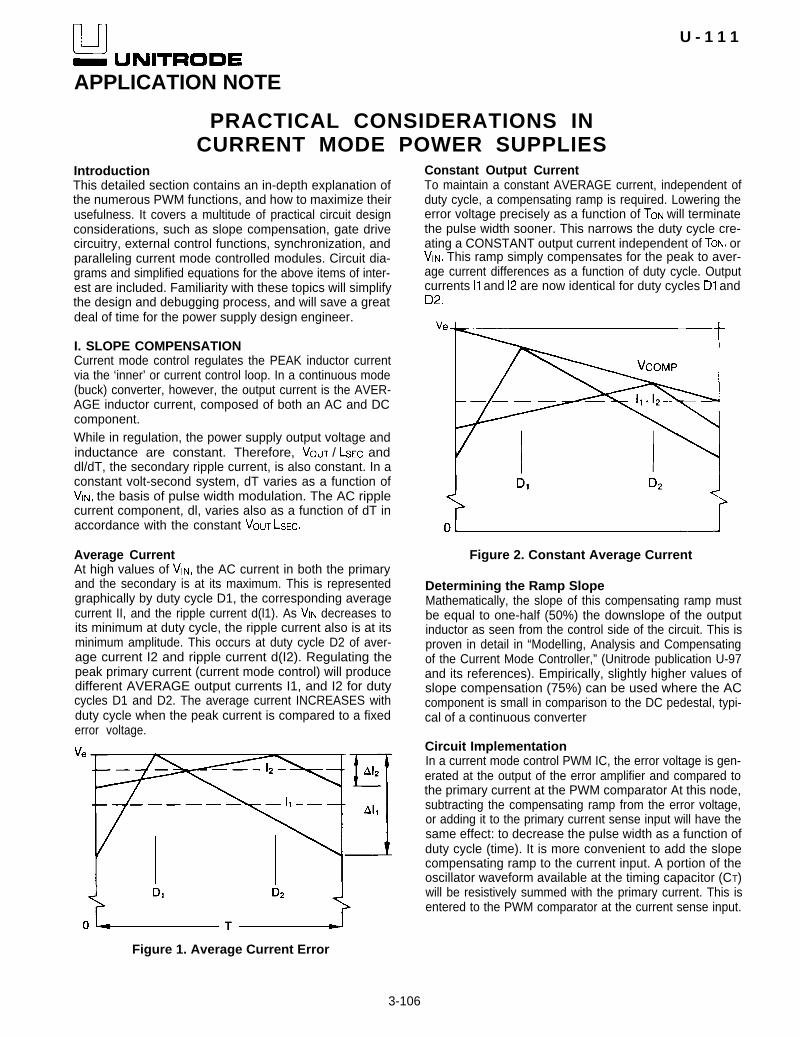
III. SYNCHRONIZATION Operation of the PWM OscillatorPower supplies have historically been thought of as “blackboxes,” an off-the-shelf commodity by most end users.Their primary function is to generate a precise voltage,independent of load current or input voltage variations, atthe lowest possible cost. In addition, end users allocate aminimal amount of system real estate in which it must fit.The major task facing design engineers is to overcomethese constraints while exceeding the customers’ expec-tations, attaining high power densities and avoidingthermal management problems. It is imperative, too, thatthe power supply harmonize and integrate with the systemrather than cause catastrophic noise problems and lastminute headaches. Products that had performed to satis-faction on the lab workbench powered by well filteredlinear supplies may not fare as well when driven by a noisyswitcher enclosed in a small cabinet.
In normal operation, the timing capacitor (Ct) is linearlycharged and discharged between two thresholds, theupper and lower comparator thresholds. The chargingcurrent is determined by means of a fixed voltage acrossa user selected timing resistance (Rt). The resulting currentis then mirrored internally to the timing capacitor Ct at theIC’s Ct output. The discharge current is internally set inmost PWM designs.
Basic power supply design criteria such as the switchingfrequency may be designated by the system clock or CPUand thus may not be up to the power supply designer’s dis-cretion. This immediately impacts the physical size of themagnetic components, hence overall supply size, and mayresult in less-than-optimum power density. However, for thesystem to function properly, the power supply must besynchronized to the system clock.
As Ct begins its charge cycle, the outputs of the PWM areinitiated and turn on. The timing capacitor charges, andwhen its amplitude equals that of the error amplifier output,the PWM output is terminated and the outputs turn off. Ctcontinues to charge until it reaches the upper threshold ofthe timing comparator Once intersected, the dischargecircuitry activates and discharges Ct until the timingcomparator lower threshold is reached. During this dis-charge time, the PWM outputs are disabled, thus insuringa “dead” time when each output is off.
There are numerous other reasons for synchronizing thepower supply to the system. Most switching power noisehas a high peak-to-average ratio of short duration,generally referred to as a spike. Common mode noise gen-erated by these pulsating currents through stray capaci-tance may be difficult (if not impossible) to completely elimi-nate after the system design is complete. Ground loopnoise may also be amplified due to the interaction ofchanging currents through parasitic inductances, resultingin crosstalk through the system. EMI filtering to the maininput line is much simpler and more repeatable whenpower is processed at a fixed frequency.
In addition, multiple power stages require synchronizationto reduce the differential noise generated between mod-ules at turn-on. In unison, the converters begin their cyclesat the same time, each contributing to common modenoise simultaneously, rather than randomly. This also sim-plifies peak power considerations and will result in predict-able power distribution and losses. Compensation madefor voltage drops along the bus bars, produced by both theAC and DC power current components, can be accom-plished. Balancing of the loads and power bus losses alsocontributes to diminishing the differential noise and shouldbe administered for optimum results.
The SYNC terminal provides a “digital” representation ofthe oscillator charge/discharge status and can be utilizedas both an input or an output on most PWM’s. In instanceswhere no synchronization port is easily available, the timingcircuitry (Ct) can be driven from a digital (0V, 5V) logic inputrather than in the analog mode. The primary considera-tions of on-time, off-time, duty cycle and frequency can beencompassed in the digital pulse train. A LOW logic levelinput determines the PWM ON time. Conversely, a HIGHinput governs the OFF time, or dead time. Critical con-straints of frequency, duty cycle or dead time can beaccurately controlled by a digital signal to the PWM timingcap (Ct) input. The command can be executed by anythingfrom a simple 555 timer, to an elaborate microprocessorsoftware controlled routine.
3-111
APPLICATION NOTE
Not all PWM IC’s have a direct synchronization input/out-put connection available to the internal oscillator In theseapplications, the slave oscillator must be disabled anddriven in a different fashion. This approach may also berequired when using different PWMs amongst the slavemodules with different sync characteristics, or anti-phasesignals.Unfortunately, there are several drawbacks to this method,depending on the implementation. First, the PWM erroramplifier has no control over the pulse width in voltagemode control. The error amplifier output is compared to adigital signal instead of a sawtooth ramp, rendering itsattempts fruitless. The conventional soft start technique ofclamping the error amp output, thereby clamping the dutycycle will not function. With no local timing ramp available,the supply is completely under the direction of the syncpulse source. Should the pulse become latched orremoved, the PWM outputs will either stay fully on, or fullyoff, depending on the sync level input (voltage mode). Also,without the local Ct ramp, the supply will not self-start,remaining off until the sync stream appears. Slope com-pensation for current mode controlled units requires addi-tional components to generate the compensating ramp.Every supply must be produced as a dedicated master, orslave, and must be non-interchangeable with one another,barring modification. This is only a brief list of the numerousdesign drawbacks to this “open-ended” sync operation. Tocircumvent these shortcomings, a universal sync circuithas been developed with the following performance fea-tures and benefits:- Sync any PWM to/from any other PWM- Sync any PWM to/from any number of other PWMs- Sync from digital levels for simple system integration- Bidirectional sync signal- Any PWM can be master or slave with no modifications- Each control circuit will start and run independently
of sync if sync signal is not present- Localized ramp at Ct for slope compensation- No critical frequency settings on each module- High speed - minimum delays- High noise immunity- Low power requirements- Remote off capability- Minimal effect on frequency, duty cycle, and dead time- Low cost and component count- Small size
Sync Circuit Operating PrinciplesThese optimal objectives can be obtained using a combi-nation of both analog and digital signal inputs. The timingcapacitor Ct input will be used as a summing junction forthe analog sawtooth and digital sync input. The PWM isallowed to run independently using its own Rt and Ctcomponents in standard configuration. When synchroni-zation is required, a digital sync pulse will be super-imposed on the Ct waveform.
U-111
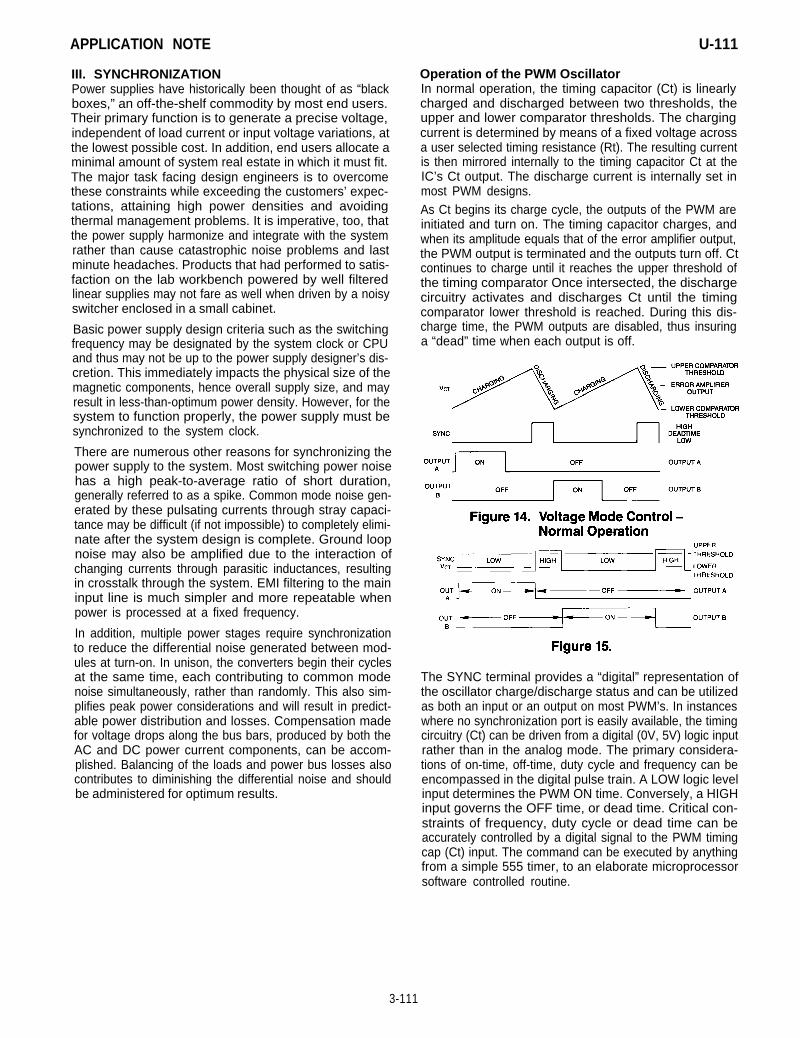
When applied, the sync pulse quickly raises the voltage atCt above the PWM comparator upper threshold. Thisforces a change in the oscillator charge/discharge statusand operation. The oscillator then begins its normal dis-charge cycle synchronized to the sync signal. This digitalsync pulse simply adds to the analog Ct waveform, forcingthe Ct input voltage above the comparator upperthreshold.
Figure 16.
In practice, this approach is best implemented by bringingCt to ground through a small resistance, about 24 ohms.This low value was selected to have minimal offset andeffects on the initial oscillator frequency. The sync pulse willbe applied across the 24 ohm resistor Since all PWMsutilize the timing capacitor in their oscillator section, it isboth a convenient and universal node to work with.
Figure 17. Sync Circuit Implementation
Oscillator Timing EquationsThe oscillator timing components must be first selected toguarantee synchronization to the sync pulse. The sawtoothamplitude must be lower than the upper threshold voltageat the desired sync frequency. If not, the oscillator will runin its normal mode and cross the upper threshold first,before the sync pulse. This requirement dictates that thePWM oscillator frequency must be lower than the syncpulse frequency to trigger reliably. Typically, a ten percentreduction in free running frequency can be accommo-dated throughout the power supply. Adding the sync cir-cuit will have minor effects on the PWM duty cycle, dead-time and ramp amplitude. (These will be examined indetail .)
3-112

APPLICATION NOTE U-111
The Timing RampAs mentioned, the timing ramp amplitude needs to beapproximately ten percent lower in frequency than normal.Therefore, the MINIMUM sync pulse amplitude must fill theremaining ten percent of the peak-to-peak ramp amplitudeto reach the upper threshold. Synchronization can beinsured over a wide range of frequency inputs and compo-nent tolerances by supplying a slightly higher amplitudesync pulse.Lowering the peak-to-peak charging amplitude also lowersthe peak-to-peak discharge amplitude. This shortens thetime required to discharge Ct since it begins at a lowerpotential. Consequently, this reduces the deadtimeaccordingly. However, the sync pulse width adds to the ICgenerated deadtime and increases the effective off, ordeadtime due to discharge. This sync pulse width needonly be wide enough to be sensed by the IC comparator,which is fairly fast. Additional sync pulse width increasesdeadtime which can be used to compensate for the 10%lower ramp, hence deadtime.
CHARGING RAMP DISCHARGING RAMP
Figure 18. Oscillator Ramp Relationships
Oscillator Ramp EquationsThe timing components required in the oscillator sectionare generally determined graphically from the manufac-turers’ data sheets for frequency and deadtime versus Rtand Ct. While fine for most applications, a careful examina-tion of the equations is necessary to analyze the impacts ofthe additional sync circuit components on the timingrelationships.
These equations can be reduced if an approximation ismade that the deadtime is very small in comparison to thetotal period. In this case, the entire effect of changing theramp voltage is upon the charging time of the oscillatorSynchronizing to a higher frequency simply reduces thecharging time of Ct, (Tchg). The new charging time (Tchg’)is the original charge time multiplied by the change in fre-quency between F original and F sync. This relativechange will be used in several equations; it is labelled P, forpercentage of change.
For small values of charging current, or large values of Rt,the voltage drop across the 24 ohm resistor is negligible. Acurrent of 2 milliamps will result in a 2.5% timing error witha 2 volt peak to peak oscillator ramp at Ct. It is also prefer-rable to free-run the IC oscillator at about a 15% lower fre-quency than the synchronization frequency, where “P” =0.85.
With an approximate 2 volt peak to peak oscillator ampli-tude, the minimum sync pulse amplitude is 0.30 volts forsynchronization to occur with a 15% latitude infrequencies.
Oscillator Discharge Ramp EquationsProper deadtime control in the switching power stage isrequired to safeguard against catastrophic failures. Add-ing the sync circuit to the oscillator reduces the dischargetime of the timing capacitor Ct, hence reducing the dead-time of the PWM. There are two contributing factors. First,the peak amplitude at the timing capacitor is lowered by AVosc(o) - AVosc’, and the capacitor begins its dischargefrom a lower potential. Second, the 24 ohm resistor addsan offset voltage, dependent on its current. Typical IC dis-charge currents range from approximately 6 to 12 milli-amps. This offset due to charging current (1-2 ma) is low incomparison to that of the discharge current (6 to 12 ma).While negligible during the charge cycle, its tenfold effectsmust be taken into account during the discharge, ordeadtime.The discharge time (T dchg) can be calculated knowingthe discharge current of the particular IC. More convenientis to use the manufacturers’ published deadtime listing fora known value of Ct, and to calculate the effects of the synccircuit. The discharge current has been averaged to 8 milli-amps for brevity.
3-113

APPLICATION NOTE U-111
The actual deadtime is a summation of both the dischargetime of Ct and the width of the sync pulse. While beingapplied, the sync pulse disables the PWM outputs andmust be added to the discharge time. The sync pulse widthcan be used to compensate for the “lost” deadtime, or asa deadtime extension.T dead’ = T dchg’ + T sync pulse width
Figure 19. Sync Circuit Schematic
Operating PrinciplesA positive going signal is input to the base of transistor Q1which operates as an emitter follower. The leading edge ofthe sync signal is coupled into the base of Q2 throughcapacitor Cl, developing a voltage across R4 in phase withthe sync input. This signal is driven through C2 to the slavetiming capacitor and 24 ohm resistor network, forcingsynchronization of the slave to the master This high speedpulse amplifier circuit adds a minimum of delay (= 50 ns)between the master to slave timing relationship.
Vertical: 1 Volt/CM Horizontal:F OSC = 1 MHz
Figure 20. Sync Circuit Waveforms
This photo displays the waveforms of the sync circuit inoperation at a clock frequency of 1 megahertz. The toptrace is the circuit input, a 2.5 volt peak-to-peak clock out-put signal from the UC3825 PWM. Any of several otherPWMs can be used as the source with similar results atlower frequencies. The center trace depicts the base toground voltage waveform at transistor Q2, biased at 3 volts.The lower trace displays the output voltage across R4 whiledriving three slave modules, or about 8 ohms from the 5volt reference.
Top Trace:Master :CT
Center Trace:Clock Output
Bottom Trace:V Sync Output
F OSC = 1 MHz
Figure 21. Circuit Timing Waveforms
Top Trace:Master Clock Output
Bottom Trace:Slave Clock Output
Both: 1 V/CM, 20 ns/CM
Figure 22. Sync Circuit Delay; Input to Output
Vertical: 1 V/CM All Horizontal:Fo = 1 MHz
Figure 23. Oscillator Waveforms:Master and Slaves
3-114
APPLICATION NOTE U-111
Vertical: 1 V/CM All Horizontal: 20 ns/CM
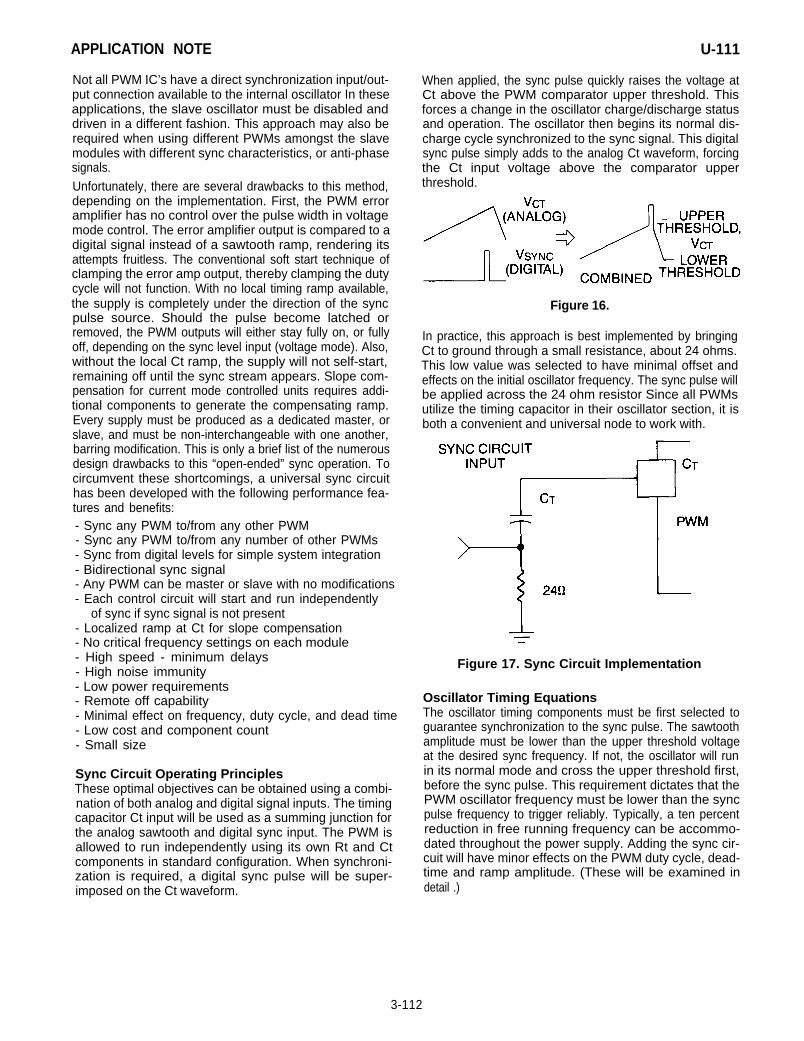
Figure 24. Typical Sync Delay at CT:Master to Slaves
Synchronization ranges for the slaves were discussed inthe previous text. The 1 volt sync pulse will accommodatemost ranges in frequency due to manufacturers’ toler-ances. The following photo is included to display the out-come of trying to use the sync circuit on slaves with oscilla-tor frequencies set beyond the sync circuit range. Theupper trace is the master Ct waveform. The center trace isCt of a slave free-running at approximately one half that ofthe master. The sync pulse alters the waveform, howeverdoes not bring it above the comparator’s upper thresholdto force synchronization. The lower trace shows a slave freerunning at approximately twice that of the master’s oscilla-tor In this instance, the sync pulse forces synchronizationat alternate cycles to the master.
trace. The amplitude should be made as large as possibleto enhance circuit performance.
Figure 26. CT Ramp Amplitude Waveforms
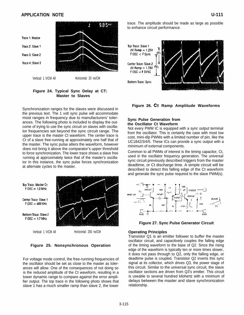
Sync Pulse Generation fromthe Oscillator Ct WaveformNot every PWM IC is equipped with a sync output terminalfrom the oscillator. This is certainly the case with most lowcost, mini-dip PWMs with a limited number of pin, like theUC1842/3/4/5. These ICs can provide a sync output with aminimum of external components.Common to all PWMs of interest is the timing capacitor, Ct,used in the oscillator frequency generation. The universalsync circuit previously described triggers from the masterdeadtime, or Ct discharge time. A simple circuit will bedescribed to detect this falling edge of the Ct waveformand generate the sync pulse required to the slave PWM(s).
Figure 27. Sync Pulse Generator Circuit
Vertical: 1 V/CM All Horizontal: 250 ns/CM
Figure 25. Nonsynchronous Operation
For voltage mode control, the free-running frequencies ofthe oscillator should be set as close to the master as toler-ances will allow. One of the consequences of not doing sois the reduced amplitude of the Ct waveform, resulting in alower dynamic range to compare against the error ampli-fier output. The top trace in the following photo shows thatslave 1 has a much smaller ramp than slave 2, the lower
Operating PrinciplesTransistor Q1 is an emitter follower to buffer the masteroscillator circuit, and capacitively couples the falling edgeof the timing waveform to the base of Q2. Since the risingedge of the waveform is typically ten or more times slower,it does not pass through to Q2, only the falling edge, ordeadtime pulse is coupled. Transistor Q2 inverts this syncsignal at its collector, which drives Q3, the power stage ofthis circuit. Similar to the universal sync circuit, the slaveoscillator sections are driven from Q3’s emitter. This circuitis useable to several hundred kilohertz with a minimum ofdelays between the master and slave synchronizationrelationship.
3-115

APPLICATION NOTE U-111
simply pulling the error amplifier output below the lowerthreshold of the PWM comparator of approximately 0.5volts. This can be easily implemented via an NPN transistorplaced between the E/A output and ground, used to shortcircuit the E/A output to zero volts. In most cases, this nodeis internally current limited to prevent failures.Another scheme is to pull the current limit or current senseinput above its upper threshold. A small transistor from thisinput to the reference voltage will fulfill this requirement.
Vertical: 0.5 V/CM Both Horizontal: 0.5 µS/CM
Figure 28. Operating Waveforms at 500 KHz
A. NONLATCHING
Figure 30. PWM Shutdown Circuits
Vertical: 0.5 V/CM Both Horizontal: 0.5 µS/CM
Figure 29. Master/Slave Sync Waveforms at CT
IV. EXTERNALLY CONTROLLING THE PWMMany of today’s sophisticated control schemes requireexternal control of the power supply for various reasons.While most of these requirements can be incorporatedquite easily with a full functioned control chip, (typical of a16 pin device), implementation may be more complex witha low cost, 8 pin PWM. Circuits to provide these functionswith a minimum of external parts will be highlighted.
ShutdownOne of the most common requirements is to provide acomplete shutdown of the power supply for certain situa-tions like remote on/off, or sequencing. Typically, a TTLlevel input is used to disable the PWM outputs. Both vol-tage and current mode control ICs can perform this task by
B. NONLATCHING
Figure 31.
Latching ShutdownFor those applications which require a latching shutdownmechanism, an SCR can be used in conjunction with theabove circuits, or in lieu of them. The SCR can also beplaced from the PWM E/A output to ground, provided thePWM E/A minimum short circuit current is greater than themaximum holding current of the SCR, and the voltagedrop at I(hold) is less than the lower PWM threshold.
3-116

APPLICATION NOTE U-111
C. LATCHING
Figure 32.
Soft StartUpon power-up, it is desirable to gradually widen the PWMpulse width starting at zero duty cycle. On PWMs withoutan internal soft start control, this can be implemented exter-nally with three components. An R/C network is used toprovide the time constant to control the I limit input or erroramplifier output. A transistor is also used to isolate the com-ponents from the normal operation of either node. It alsominimizes the loading effects on the R/C time constant byamplification through the transistors gain.
B. USING E/A
Figure 33.
Variable Frequency OperationCertain topologies and control schemes require the use ofa variable frequency oscillator in the controlling element.However, most PWMs are designed to operate in a fixedfrequency mode of operation. A simple circuit is presentedto disable the ICs internal oscillator between pulses, thusallowing variable frequency operation.Internal at the ICs timing resistor (Rt) terminal is a currentmirror The current flowing through Rt is duplicated at theCt terminal during the charge cycle, or “on” time. When theRt terminal is raised to V ref (5 volts), the current mirror isturned off, and the oscillator is disabled. This is easilyswitched by a transistor and external logic as the controlelement, for example, a pulse generator. The PWM’s timingresistor and capacitor should be selected for the maximum“ON” time and minimum “DEAD” time of the PWMoutput(s). The rate at which the PWM oscillator is disableddetermines the frequency of the output(s).The frequency can be varied in two distinct fashionsdepending on the desired control mode and triggersource. The “off” time of both outputs will occur on a pulse-by-pulse basis when the PWM outputs are OR’d to the trig-ger source. In this configuration either output initiates the“off” time, triggered by its falling edge. The PWM output Ais activated, then both outputs A and B are low during the“off” time of the pulse generator. This is followed by outputB being activated, then both outputs A and B low againduring the next “off” time. This cycle repeats itself at a fre-quency determined by the pulse generator circuitry.Another method is to introduce the “off” time after two(alternate A, then B) output pulses. Output A is activated,followed immediately by output B, then the desired “off”time. The pulse generator circuitry is triggered by thePWM’s falling edge of output B. The specific controlscheme utilized will depend on the power supply topologyand control requirements.
Figure 34. Oscillator Disable CircuitVariable Frequency Operation
3-117

APPLICATION NOTE U-111
VOLTAGE CONTROLLED OSCILLATORGENERAL CONFIGURATIONVARIABLE FREQUENCY OPERATION
FIXED 50% DUTY CYCLEOSCILLATORS WITH SINGLE PIN PROGRAMMING
UC3851 / UC3844A / UC3845A*GROUND RAMP OR CURRENT SENSE INPUT
OSCILLATORS WITH SEPARATE RT & CT PINS
U C 3 8 2 3 / U C 3 8 2 5 / U C 3 8 4 7*GROUND RAMP OR CURRENT SENSE INPUT
USE NONINV E/a INPUT FOR REVERSE V/F OPERATION
Fixed “Off -Time” ApplicationsObtaining a fixed “off-time” and a variable “on-time” caneasily be accomplished with most current-mode PWM IC’s.In these applications, the Rt/Ct timing components are usedto generate the “off-time” rather than the traditional “on-time.” Implementation is shown schematically in Figure 3along with the pertinent waveforms.
At the beginning of an oscillator cycle, Ct begins chargingand the PWM output is turned on. Transistor Q1 is drivenfrom the output and also turns on with the PWM output, thusdischarging Ct and pulling this node to ground. As thisoccurs, the oscillator is “frozen” with the PWM output fullyON. On-time can be controlled in the conventional mannerby comparing the error amplifier output voltage with thecurrent sense input voltage. This results in a current con-trolled “on-time” and fixed “off-time” mode of operation.Other variations are possible with different inputs to thecurrent sense input.When the PWM output goes low (off ), transistor Q1 also turnsoff and Ct begins charging to its upper threshold.The off-timegenerated by this approach will be longer for a given Rt/Ctcombination than first anticipated using the oscillator"charg-ing” equations or curves. Timing capacitor Ct now beginscharging from Vsat of Q1 (approx. 0V) instead of the internaloscillator lower threshold of approximately 1 volt.
FIXED “OFF-TIME”, CURRENTCONTROLLED “ON-TIME”
SCHEMATIC
WAVEFORMS
Figure 35.
3-118

APPLICATION NOTE U-111
Current Mode ICs Used in Voltage ModeMost of today’s current mode control ICs are second andthird generation PWMs. Their features include high currentoutput driver stages, reduced internal delays through theirprotection circuitry, and vast improvements in the refer-ence voltage, oscillator and amplifier sections. In compari-son to the first generation ICs (1524), numerous advan-tages can be obtained by incorporating a second or thirdgeneration IC (18XX) into an existing voltage mode design.In duty cycle control (voltage mode), pulse width modula-tion is attained by comparing the error amplifier output toan artificial ramp. The oscillator timing capacitor Ct is usedto generate a sawtooth waveform on both current or vol-tage mode ICs. To utilize a current mode chip in the voltagemode, this sawtooth waveform will be input to the currentsense input for comparison to the error voltage at the PWMcomparator. This sawtooth will be used to determine pulsewidth instead of the actual primary current in this method.
Figure 36. Current Mode PWM Used as aVoltage Mode PWM
Compensation of the loop is similar to that of voltage mode,however, subtle differences exist. Most of the earlier PWMs(15xx) incorporate a transconductance (current) typeamplifier, and compensation is made from the E/A outputto ground. Current mode PWMs use a low output resis-tance (voltage) amplifier and are compensated accord-ingly. For further reference on topologies and compensa-tion, consult “Closing the Feedback Loop” listed in thisappendix.
VI. FULL DUTY CYCLE (100%) APPLICATIONSMany of the higher power (>500 watt) power suppliesincorporate the use of a fan to provide cooling for the mag-netic components and semiconductors. Other users lo-cate fans throughout a computer mainframe, or otherequipment to circulate the air and keep temperatures fromskyrocketing. In either case, the power supply designer isusually responsible for providing the power and control.The popularity of low voltage DC fans has increasedthroughout the industry due to the stringent agency safetyrequirements for high voltage sections of the overall circuit.In addition, it’s much easier to satisfy dual AC inputs andfrequency stipulations with a low cost DC fan, powered bya semi-regulated secondary output.The most efficient way to regulate the fan motor speed(hence temperature) is with pulse width modulation. Anerror signal proportional to temperature can be used as thecontrol voltage to the PWM error amplifier. While nearly fullduty cycle can be easily attained, the circumstances maywarrant full, or true 100% duty cycle.This condition is highly undesirable in a switch-modepower supply, therefore most PWM IC designs have goneto great extent to prevent 100% duty cycle from occurring.There are simple ways to over-ride these safeguards, how-ever. One method, presented below, “freezes” the oscilla-tor and holds the PWM output in the ON, or high statewhen the circuit is activated. Feedback from the output isrequired to guarantee that the oscillator is stopped whilethe output is high. Without feedback, the oscillator can benulled with the output in either state.
Figure 37. Full Duty Cycle Implementation
3-119
APPLICATION NOTE
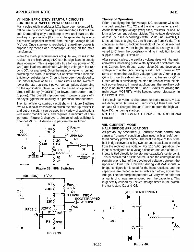
VII. HIGH EFFICIENCY START-UP CIRCUITSFOR BOOTSTRAPPED POWER SUPPLIESMany pulse width modulator I.C.s have been optimized foroffline use by incorporating an under-voltage lockout cir-cuit. Demanding only a milliamp or two until start-up, theauxiliary supply voltage (V aux) can be generated by a sim-ple resistor/capacitor network from the high voltage dc rail(+V dc). Once start-up is reached, the auxiliary power issupplied by means of a “boostrap” winding on the maintransformer.While the start-up requirements are quite low, losses in theresistor to the high voltage DC can be significant in steadystate operation. This is especially true for low power (< 35watt) applications and circuits with high voltage rails (400volts DC, for example). Once the main converter is running,switching the start-up resistor out of circuit would increaseefficiency substantially. Circuits have been developed touse either bipolar or MOSFET transistors as the switch tolower the start-up circuit power consumption, dependingon the application. Selection can be based on optimizingcircuit efficiency (MOSFET) or lowest component cost(bipolar). The overall improvement in power supply effi-ciency suggests this circuitry is a practical enhancement.The high efficiency start-up circuit shown in figure 1 utilizestwo NPN bipolar transistors to switch the start-up resistor inand out of circuit. It can be used in a variety of applicationswith minor modifications, and requires a minimum of com-ponents. Figure 2 displays a similar circuit utilizing Nchannel MOSFET devices to perform the switching.
Figure 38. NPN Switches
U-111
Theory of OperationPrior to applying the high voltage DC, capacitor Cl is dis-charged; switches Q1, Q2 and the main converter are off.As the input supply voltage (Vdc) rises, resistors R1 and R2form a low current voltage divider. The voltage developedacross R2 rises accordingly with +V dc until switch Q1turns on, thus charging C1 thru R start-up from +V dc. Thiscontinues as the UV lockout threshold of the I.C. is reachedand the main converter begins operation. Energy is deli-vered to Cl from the bootstrap winding in addition to thatsupplied through R start-up.After several cycles, the auxiliary voltage rises with the mainconverters increasing pulse width, typical of a soft-start rou-tine. Current flows through zener diode D1 and develops avoltage across the Q2’s biasing resistor, R3. Transistor Q2turns on when the auxiliary voltage reaches V zener plusQ2’s turn on threshold. As this occurs, transistor Q1 isturned off, thus eliminating the start-up resistor from the cir-cuit power losses. In most applications, the auxiliary vol-tage is optimized between 12 and 15 volts for driving themain power MOSFETs, while keeping power dissipation inthe PWM IC low.If the main converter is shut down for some reason, V auxwill decay until Q2 turns off. Transistor Q1 then turns backon, and Cl is charged through R start-up from the high vol-tage DC, as during start-up.NOTE: SEE DESIGN NOTE DN-26 FOR ADDITIONALCIRCUITS.
VIII. CURRENT MODEHALF BRIDGE APPLICATIONSAs previously described (1), current mode control cancause a “runaway” condition when used with a “soft” cen-tered primary power source. The best example of this is thehalf bridge converter using two storage capacitors in seriesfrom the rectified line voltage. For 110 VAC operation, theinput is configured as a voltage doubler, and one of the ACinputs is tied directly to the storage capacitor’s centerpoint.This is considered a “stiff” source, since the centerpoint willremain at one-half of the developed voltage between theupper and lower rail. However, during 220 VAC inputs, abridge configuration is used for the input rectifiers, and thecapacitors are placed in series with each other, across thebridge. Their centerpoint potential will vary when differentamounts of charge are removed from the capacitors. Thisis generally caused by uneven storage times in the switch-ing transistors Q1 and Q2.
STIFF CENTERPOINT
Figure 39.
3-120 Figure 40.

APPLICATION NOTE U-111
SOFT CENTERPOINT
Figure 41.
The centerpoint voltage can be maintained at one-half+Vdc by the use of a balancing technique. In normaloperation, transistor Q1 turns on, and the transformer pri-mary is placed across one of the high voltage capacitors,C1 for example. On alternate cycles the transformer pri-mary is across the other cap, C2. An additional balancingwinding, equal in number in turns to the primary, is woundon the transformer. It is connected also to the capacitorcenterpoint at one end and thru diodes to each supply railat the other end. The phasing is such that it is in series withthe primary winding through the ON time of eithertransistor Q1 or Q2.
Figure 42. Schematic - Balancing Winding
In this configuration, the center point of the high voltagecaps is forced to one-half of the input DC voltage by natureof the two series windings of identical turns. Should themidpoint begin to drift, current flows thru the balancingwinding to compensate.
Figure 44. Transistor Q2 On
In most high frequency MOSFET designs, the FET mis-matches are small, and the average current in the balanc-ing winding is less than 50 milliamps. A small diameter wirecan be wound next to the larger sized primary for thebalancing winding with good results.
IX. PARALLELING CURRENT MODE MODULESOne of the numerous advantages of current mode controlis the ability to easily parallel several power supplies for in-creased output power. This discussion is intended as aprimer course to explore the basic implementationscheme and design considerations of paralleling thepower modules. Redundant operation, failure modes andtheir considerations are not included in this text.The prerequisites for parallel operation are few in number,but important to insure proper operation. First, each powersupply module must be current mode controlled, andcapable of supplying its share of the total output power. Allmodules must be synchronized together, and one unit canbe designated as the master for the sake of simplicity. Allremaining units will be configured as slaves.The master will perform one function in addition to gen-erating the operating frequency. It provides a commonerror voltage (Ve) to all modules as the input to the PWMcomparator. This voltage is compared to the individualmodule’s primary current at its PWM comparator. Theslaves are utilized with their error amplifier configured inunity gain. Assume there are identical primary currentsense resistors in each module, and no internal offsets inthe ICs amplifiers or other circuit components. In this case,the output voltages and currents of each module would beidentical, and the load would be shared equally among themodules.
Figure 45. PWM Diagram
Figure 43. Transistor Q1 On
3-121

APPLICATION NOTE
In reality, small offets of ± 10 millivolts exist in each PWMamplifier and comparator. As the common error voltage,(Ve) traverses through the IC’s circuitry, its accuracy de-creases by the number and quality of gates in its path. Themaximum error occurs at the lowest common mode ampli-fier voltage, approximately 1 volt. The ± 20 millivolt offsetrepresents a ± 2% error at the PWM comparator. At highercommon mode voltages, typical of full load conditions, theerror voltage (Ve) is closer to its maximum of 4 volts. Herethe same ± 20 millivolts introduces only ± 0.5% error to thesignal.The other input to the PWM comparator, Vr, is the voltagedeveloped by the primary current flowing through the cur-rent sense resistor(s). In many applications, a 5% toleranceresistor is utilized resulting in a ± 5% error at the PWMcomparator’s “current sense” or ramp input.Pulse width is determined by comparing the error voltage(Ve) with the current sense voltage, (Vr). When equal, theprimary current is therefore the error voltage divided by thecurrent sense resistance; Ip = Ve/Rs. Output current isrelated to the primary current by the turns ratio (N) of thetransformer. Sharing of the load, or total output current isdirectly proportional to the sharing of the total primary cur-rent. The previous equations and values can be used todetermine the percentage of sharing between modules.
Unit 1Unit 1 Unit 2Unit 2
U-111
Primary current, Ip = Ve/Rs. Introducing the tolerances,Ip’ = Ve (± 2%) / Rs (± 5%); therefore Ip’ = Ip (± 7%)The primary currents (hence output currents) will sharewithin ± seven percent (7%) of nominal using a five per-cent sense resistor. Clearly, the major contribution is fromthe current sense circuitry, and the PWM IC offsets areminimal. Balancing can be improved by switching to atighter tolerance resistor in the current sense circuitry.The control-to-output gain (K) decreases with increasingload. At high loads, when primary currents are high, so isthe error amplifier output voltage, (Ve). With a typical valueof four volts, the effects of the offset voltages are minimized.This helps to promote equal sharing of the load at fullpower, which is the intent behind paralleling severalmodules.For demonstration purposes, four current mode push-pullpower supplies were run in parallel at full power. The pri-mary current of each was measured (lower traces) andcompared to a precision 1 volt reference (upper trace). Thevoltage differential between traces is displayed in theupper right hand corner of the photos. Using closelymatched sense resistors, the peak primary currents variedfrom a low of 2.230A to 2.299 amps. Calculating a meanvalue of 2.270 amps, the individual primary currentsshared within two percent, indicative of the sense resistortolerances.
Unit 3Unit 3 Unit 4Unit 4
Figure 46. Primary Currents - Parallel Operation
3-122

APPLICATION NOTE
Other factors contributing to mismatch of output power arethe individual power supply diode voltage drops. The out-put choke inductance reflects back to the primary currentsense, and any tolerances associated with it will alter theprimary current slope, hence current. In the control sec-tion, the peak-to-peak voltage swing at the timing capacitorCt effects the amount of slope compensation introduced,along with the tolerance of the summing resistor Thesemust all be accounted for to calculate the actual worst casecurrent sharing capability of the circuit.
Top Trace:VE: Error Voltagewith Noise
Lower Trace:VR: PrimaryCurrent
PARALLELOPERATIONEQUAL LEADLENGTHS FROMMASTER ANDSLAVE(S) TO ALLC O N N E C T I O N S
Figure 47. Noise Modulating VE
Proper layout of all interconnecting wires is required toinsure optimum performance. Shielded coax cable isrecommended for distributing the error voltage among themodules. Any noise on this line will demonstrate its impactat the PWM comparator, resulting in poor load sharing, orjitter.
UNITRODE CORPORATION
U-111
C a b l e s s h o u l d b e o f e q u a l l e n g t h , o r i g i n a t i n g a t t h e
mas te r and rou ted away f r om any no i se sou rces , l i ke t he
high vol tage switching sect ion. Al l input and output power
l eads shou ld be exac t l y t he same l eng th and w i re gauge ,
connec ted t oge the r a t ONE s ing le po in t . Leads shou ld be
treated as resistors in ser ies wi th the load, and deviat ions
in length wi l l resul t in di f ferent currents del ivered from each
m o d u l e .
F i g u r e 4 8 .
7 CONTINENTAL BLVD.. MERRIMACK. NH 03054TEL. (603) 424-2410 l FAX (603) 424-3460 3-123

IMPORTANT NOTICE
Texas Instruments and its subsidiaries (TI) reserve the right to make changes to their products or to discontinueany product or service without notice, and advise customers to obtain the latest version of relevant informationto verify, before placing orders, that information being relied on is current and complete. All products are soldsubject to the terms and conditions of sale supplied at the time of order acknowledgement, including thosepertaining to warranty, patent infringement, and limitation of liability.
TI warrants performance of its semiconductor products to the specifications applicable at the time of sale inaccordance with TI’s standard warranty. Testing and other quality control techniques are utilized to the extentTI deems necessary to support this warranty. Specific testing of all parameters of each device is not necessarilyperformed, except those mandated by government requirements.
CERTAIN APPLICATIONS USING SEMICONDUCTOR PRODUCTS MAY INVOLVE POTENTIAL RISKS OFDEATH, PERSONAL INJURY, OR SEVERE PROPERTY OR ENVIRONMENTAL DAMAGE (“CRITICALAPPLICATIONS”). TI SEMICONDUCTOR PRODUCTS ARE NOT DESIGNED, AUTHORIZED, ORWARRANTED TO BE SUITABLE FOR USE IN LIFE-SUPPORT DEVICES OR SYSTEMS OR OTHERCRITICAL APPLICATIONS. INCLUSION OF TI PRODUCTS IN SUCH APPLICATIONS IS UNDERSTOOD TOBE FULLY AT THE CUSTOMER’S RISK.
In order to minimize risks associated with the customer’s applications, adequate design and operatingsafeguards must be provided by the customer to minimize inherent or procedural hazards.
TI assumes no liability for applications assistance or customer product design. TI does not warrant or representthat any license, either express or implied, is granted under any patent right, copyright, mask work right, or otherintellectual property right of TI covering or relating to any combination, machine, or process in which suchsemiconductor products or services might be or are used. TI’s publication of information regarding any thirdparty’s products or services does not constitute TI’s approval, warranty or endorsement thereof.
Copyright 1999, Texas Instruments Incorporated


![PRACTICAL CONSIDERATIONS - Aalborg Universitethomes.nano.aau.dk/lg/Biosensors2009_files/Wang_Ch4.pdf · 118 PRACTICAL CONSIDERATIONS (DMF), dimethylsulfoxide (DMSO), or methanol]](https://img.dokumen.tips/doc/110x75/5a8645f77f8b9a882e8cc8c2/practical-considerations-aalborg-practical-considerations-dmf-dimethylsulfoxide.jpg)