Embed Size (px)
Citation preview
• •Specifications subject to change without notice. 2016 Littelfuse, Inc.September 19, 2016 - Rev. 2
1 Publication Order Number:AN004E/D
ABSTRACTThis paper addresses the requirements for the
semiconductor sensing circuitry and SCR crowbar devicesused in DC power supply over/under voltage protectionschemes.
INTRODUCTIONIt is uncommon now to find several hundred dollars
worth of microprocessors and memory chips powered froma single low DC supply.
If this supply on the board doesn’t have overvoltage orundervoltage protection, potentially large sums of moneycan literally go up in smoke due to component failure, or,for instance, a tool may be accidentally dropped across thesupply buses of different voltages during testing or repairof the system.
Since a couple of years, computer and industrialmanufacturers agree to put additional small investment inOver Voltage Protection (OVP) and Over/Under VoltageProtection (OUVP) circuitry to prevent disasters.
Littelfuse chose the “crowbar” sensing circuittechnology. This system senses the overvoltage condition,and quickly “crowbars” or short circuits the supply, forcingthe supply into current limiting or opening the fuse orcircuit breaker. Before detailing this technology, threequestions should be considered:
1. Why OVP? To save money and increase thereliability of the system.
2. Where OVP?–Everywhere over/under voltage is a problem.–Everywhere a power supply system is used.–Everywhere a switchmode system is designed.
3. How OVP? There are several types of sensecircuits presently being used in OVP applications.They can be classified into three types:a) Zenerb) Discretec) MC1723 (voltage regulator in OVP
configuration)
This document may contain references to devices which are nolonger offered. Please contact your Littelfuse representativefor information on possible replacement devices.
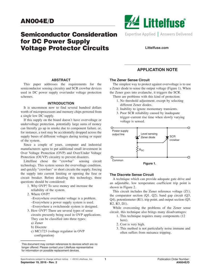
The Zener Sense CircuitThe simplest way to protect against overvoltage is to use
a Zener diode to sense the output voltage (Figure 1). Whenthe Zener goes into avalanche, it triggers the SCR.
There are problems with this kind of protection:1. No threshold adjustment, except by selecting
different Zener diodes.2. Inability to ignore momentary transients.3. Poor SCR reliability caused by inadequate
trigger–current rise time when slowly varyingvoltage is sensed.
Power supplyoutput line
Common
RSC
SCRcrowbar
Level sensingZener diode
Figure 1.
The Discrete Sense CircuitA technique which can provide adequate gate drive and
an adjustable, low temperature coefficient trip point isshown in Figure 2.
This circuit includes the Zener reference voltage (Z1),the comparator section (Q1, Q2), band gap circuit (Q3,Q4), potentiometer (R1), trip point, and output section (Q5,R2, R3, D1).
While overcoming the problems of the Zener sensecircuit, this technique also brings many disadvantages:
1. This technique requires many components (12here).
2. Cost is very high.3. This method is not particularly noise immune and
often suffers from nuisance tripping.
APPLICATION NOTE
Littelfuse.com
AN004E/D
2
Z1
Figure 2.
Q1
Q4Q3
Q2
Q5
R1
R3
R2D1
Figure 3.
–
+
The MC1723 Sense CircuitA simpler approach is to fire the SCR crowbar with an
MC1723 voltage regulator.A considerable reduction in component count is done
(see Figure 3). The main disadvantages are:1. No noise immunity.2. The minimum input voltage range is 9.5 V, so
you are restricted to use it for higher voltages orto supplement it by feeding in an auxiliary supplyvoltage.
THE SCR CHOICEThe use of the SCR crowbar overvoltage protection
circuits in DC power supplies has been, for many years, apopular method of providing protection to the load fromaccidental overvoltage stresses. This technique and itsproper implementation have become increasinglyimportant in light of the recent advances in LSI made by thesemiconductor industry.
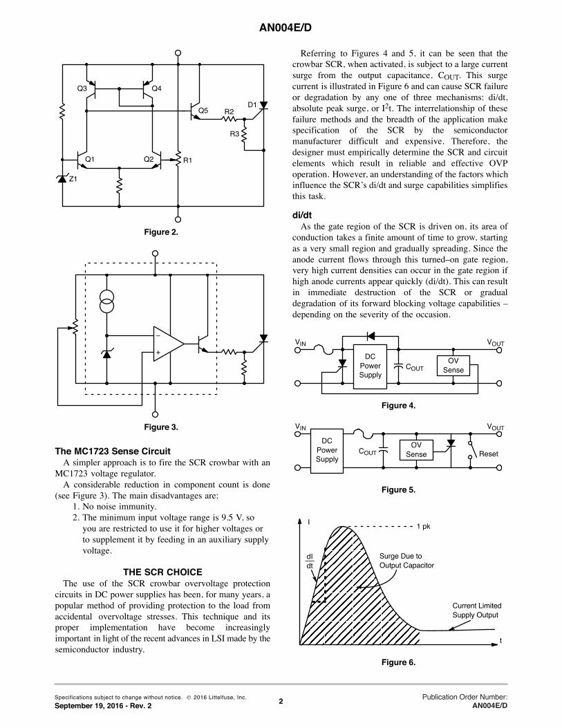
Referring to Figures 4 and 5, it can be seen that thecrowbar SCR, when activated, is subject to a large currentsurge from the output capacitance, COUT. This surgecurrent is illustrated in Figure 6 and can cause SCR failureor degradation by any one of three mechanisms: di/dt,absolute peak surge, or I2t. The interrelationship of thesefailure methods and the breadth of the application makespecification of the SCR by the semiconductormanufacturer difficult and expensive. Therefore, thedesigner must empirically determine the SCR and circuitelements which result in reliable and effective OVPoperation. However, an understanding of the factors whichinfluence the SCR’s di/dt and surge capabilities simplifiesthis task.
di/dtAs the gate region of the SCR is driven on, its area of
conduction takes a finite amount of time to grow, startingas a very small region and gradually spreading. Since theanode current flows through this turned–on gate region,very high current densities can occur in the gate region ifhigh anode currents appear quickly (di/dt). This can resultin immediate destruction of the SCR or gradualdegradation of its forward blocking voltage capabilities –depending on the severity of the occasion.
Figure 4.
VIN VOUT
DCPowerSupply
COUTOV
Sense
Figure 5.
VIN VOUT
DCPowerSupply
COUTOV
Sense Reset
Figure 6.
I
t
dIdt
1 pk
Surge Due toOutput Capacitor
Current LimitedSupply Output
Specifications subject to change without notice. 2016 Littelfuse, Inc.September 19, 2016 - Rev. 2
Publication Order Number:AN004E/D

AN004E/D
3
Figure 7.
OutputCap
ESR
ESL
R
L
LLRL
COUT consists of the power supply output caps, the load’sdecoupling caps, and in the case of Figure 4, the supply’sinput filter caps.
The value of di/dt that an SCR can safely handle isinfluenced by its construction and the characteristics of thegate drive signal. A center–gate–fire SCR has more di/dtcapability than a corner–gate–fire type and heavilyoverdriving (3 to 5 times IGT) the SCR gate with a fast(< 1 μs) rise time signal will maximize its di/dt capability.A typical maximum number in phase control SCRs of lessthan 50 Arms rating might be 200 A/μs, assuming a gatecurrent of five times IGT and < 1 μs rise time. If having donethis, a di/dt problem is seen to still exist, the designer canalso decrease the di/dt of the current waveform by addinginductance in series with the SCR, as shown in Figure 7. Ofcourse, this reduces the circuit’s ability to rapidly reducethe DC bus voltage and a tradeoff must be made betweenspeedy voltage reduction and di/dt.
Surge CurrentIf the peak current and/or the duration of the surge is
excessive, immediate destruction due to device overheatingwill result. The surge capability of the SCR is directlyproportional to its die area. If the surge current cannot be
reduced (by adding series resistance – see Figure 7) to a safelevel which is consistent with the system’s requirements forspeedy bus voltage reduction, the designer must use ahigher current SCR. This may result in the average currentcapability of the SCR exceeding the steady state currentrequirements imposed by the DC power supply.
OVERVOLTAGE PROTECTOR: THE MC3423To fill the need for a low cost, low complexity method or
implementing crowbar overvoltage protection which doesnot suffer the disadvantages of previous techniques, Littelfuse has developed the MC3423 and its militaryrange version, the MC3523.
This circuit was designed to provide output currents ofup to 300 mA with a 400 mA/μs rise time in order tomaximize the di/dt capabilities of the crowbar SCR. Inaddition, its main features include:• Operation off 4.5 V to 36 V supply voltages• Adjustable, low temperature coefficient trip point• Adjustable minimum overvoltage duration before
actuation (0.5 μs to 1.0 ms) to reduce nuisancetripping in noisy environments
• Remote activation input• Activation indication output• Output short circuit protected for VCC ≤ 10 V
The Block DiagramThe block diagram of the MC3423 is shown in Figure 8.
It consists of a stable 2.6 V reference, two comparators anda high current output.
This output, together with the indication output transistor,is activated either by a voltage greater than 2.6 V on pin 3or by a TTL/5 V CMOS high logic level on the remoteactivation input, pin 5.
–
+
VCC
Vsense1
VREF 2.6 V
+
–
Isource
+–
2
7 3 5 6VEE Vsense2 IndicatorOutputRemote
Activation
4
8
Current Source
Output
Figure 8.
Specifications subject to change without notice. 2016 Littelfuse, Inc.September 19, 2016 - Rev. 2
Publication Order Number:AN004E/D

AN004E/D
4
The first comparator is designed to initiate a stable timedelay and the second one activates both a crowbar firingcurrent and a low level indication signal.
The Basic CircuitThe basic circuit configuration of the OVP is shown in
Figure 9. In this circuit, the voltage sensing inputs of boththe internal amplifiers are tied together for sensing theovervoltage condition. The shortest possible propagationdelay is thus obtained.
The threshold on trip voltage at which the MC3423 willtrigger and supply gate drive to the crowbar SCR, Q1, isdetermined by the selection of R1 and R2. Their values canbe determined by the equation (1):
Vtrip VREF 1 R1R2 2.6 V 1 R1
R2(1)
R2 ≤ kΩ for minimum drift.Figure 10 shows (with R2 = 2.7 kΩ) the value (min, typ,
max) of R1 versus trip voltage.The switch S1, shown in Figure 9, may be used to reset
the SCR crowbar. Otherwise, the power supply, acrosswhich the SCR is connected, must be shut down to reset thecrowbar. If a non–current–limited supply is used, a fuse orcircuit breaker, F1, should be used to protect the SCRand/or the load.
The minimum value of the gate current limiting resistor,RG, is given in Figure 11. Using this value of RG the SCRQ1 will receive the greatest gate current possible withoutdamaging the MC3423. If lower output currents arerequired, RG can be increased in value.
THE PROGRAMMATION
Low Voltage < 36 VIn many instances, the MC3423 will be used in a noise
environment. To prevent false tripping of the OVP circuitby noise which would not normally harm the load, theMC3423 has a programmable delay feature. To implementthis feature, the circuit configuration of Figure 12 is used.In this configuration, a capacitor is connected from pin 3 toVEE. The value of this capacitor determines the minimumduration of the overvoltage condition which is necessary totrip the OVP. The value of C can be found from Figure 13.The circuit operates in the following manner: when VCCrises above the trip point set by R1 and R2, an internalcurrent source (pin 4) begins charging the capacitor, C,connected to pin 3. If the overvoltage condition disappearsbefore this occurs, the capacitor is discharged at a rate 10times faster than the charging rate, resetting the timingfeature until the next overvoltage condition occurs.
Figure 9.
PowerSupply MC3423
18
R1
R2
(+ SenseLead)
ToLoad
F1
23
4 7 5
(– Sense Lead)S1
+
–
RG
Figure 10.
0
20
30
R1, R
esist
ance
(kΩ
)
0VT, Trip Voltage (V)
030.5
10
10 15 20 25
Max
Min
TypR2 = 2.7 kFigure 11.
10
20
30
35
V CC,
Sup
ply
Volta
ge (V
)
0RG, Gate Current Limiting Resistor (Ω)
0801
25
15
20 30 40 50 60 70
RG(min) = 0if VCC < 11 V
Figure 12.
PowerSupply MC3423
1
8
R1
R2
2
5 7
+VCC
RG4 3
C
6
R3V10
IndicationOut
VOVC R3 ≥
Vtrip10 mA
Q1
2N6504 orequivalent
©Specifications subject to change without notice. 2016 Littelfuse, Inc.September 19, 2016 - Rev. 2
Publication Order Number:AN004E/D
AN004E/D
5
Figure 13.
0.0001
0.001
0.1
1.0C
apac
itanc
e (μ
F)
0.001td, Delay Time (ms)
0110.0
0.01
0.1 1.0
Occasionally, it is desired that immediate crowbarring ofthe supply occurs when a high overvoltage conditionoccurs, while retaining the false tripping immunity ofFigure 12.
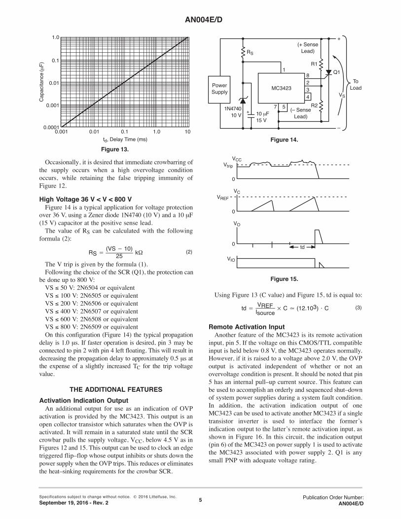
High Voltage 36 V < V < 800 VFigure 14 is a typical application for voltage protection
over 36 V, using a Zener diode 1N4740 (10 V) and a 10 μF(15 V) capacitor at the positive sense lead.
The value of RS can be calculated with the followingformula (2):
RS(VS 10)
25 k (2)
The V trip is given by the formula (1).Following the choice of the SCR (Q1), the protection can
be done up to 800 V:VS ≤ 50 V: 2N6504 or equivalentVS ≤ 100 V: 2N6505 or equivalentVS ≤ 200 V: 2N6506 or equivalentVS ≤ 400 V: 2N6507 or equivalentVS ≤ 600 V: 2N6508 or equivalentVS ≤ 800 V: 2N6509 or equivalentOn this configuration (Figure 14) the typical propagation
delay is 1.0 μs. If faster operation is desired, pin 3 may beconnected to pin 2 with pin 4 left floating. This will result indecreasing the propagation delay to approximately 0.5 μs atthe expense of a slightly increased TC for the trip voltagevalue.
THE ADDITIONAL FEATURESActivation Indication Output
An additional output for use as an indication of OVPactivation is provided by the MC3423. This output is anopen collector transistor which saturates when the OVP isactivated. It will remain in a saturated state until the SCRcrowbar pulls the supply voltage, VCC, below 4.5 V as inFigures 12 and 15. This output can be used to clock an edgetriggered flip–flop whose output inhibits or shuts down thepower supply when the OVP trips. This reduces or eliminatesthe heat–sinking requirements for the crowbar SCR.
Figure 14.
PowerSupply
MC3423
18234
RS
(+ SenseLead)
7 5 (– SenseLead)
+
–
+1N474010 V 10 μF
15 V
R1
R2
Q1
VS
ToLoad
td
Figure 15.
VCC
VC
VO
Vtrip
VREF
0
0
0
VIO
Using Figure 13 (C value) and Figure 15, td is equal to:
td VREFIsource
C (12.103) C (3)
Remote Activation InputAnother feature of the MC3423 is its remote activation
input, pin 5. If the voltage on this CMOS/TTL compatibleinput is held below 0.8 V, the MC3423 operates normally.However, if it is raised to a voltage above 2.0 V, the OVPoutput is activated independent of whether or not anovervoltage condition is present. It should be noted that pin5 has an internal pull–up current source. This feature canbe used to accomplish an orderly and sequenced shut–downof system power supplies during a system fault condition.In addition, the activation indication output of oneMC3423 can be used to activate another MC3423 if a singletransistor inverter is used to interface the former’sindication output to the latter’s remote activation input, asshown in Figure 16. In this circuit, the indication output(pin 6) of the MC3423 on power supply 1 is used to activatethe MC3423 associated with power supply 2. Q1 is anysmall PNP with adequate voltage rating.
©Specifications subject to change without notice. 2016 Littelfuse, Inc.September 19, 2016 - Rev. 2
Publication Order Number:AN004E/D
AN004E/D
6
Figure 16.
1
PowerSupply
#1
+
–
PowerSupply
#2
+
–
1
5
6
7
7
R110 k
Q1
1 k
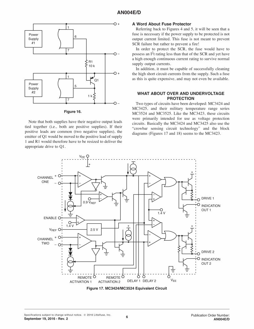
Note that both supplies have their negative output leadstied together (i.e., both are positive supplies). If theirpositive leads are common (two negative supplies), theemitter of Q1 would be moved to the positive lead of supply1 and R1 would therefore have to be resized to deliver theappropriate drive to Q1.
A Word About Fuse ProtectorReferring back to Figures 4 and 5, it will be seen that a
fuse is necessary if the power supply to be protected is notoutput current limited. This fuse is not meant to preventSCR failure but rather to prevent a fire!
In order to protect the SCR, the fuse would have topossess an I2t rating less than that of the SCR and yet havea high enough continuous current rating to survive normalsupply output currents.
In addition, it must be capable of successfully cleaningthe high short circuit currents from the supply. Such a fuseas this is quite expensive, and may not even be available.
WHAT ABOUT OVER AND UNDERVOLTAGEPROTECTION
Two types of circuits have been developed: MC3424 andMC3425, and their military temperature range seriesMC3524 and MC3525. Like the MC3423, these circuitswere primarily intended for use as voltage protectioncircuits. Basically the MC3424 and MC3425 also use the“crowbar sensing circuit technology” and the blockdiagrams (Figures 17 and 18) seems to the MC3423.
Figure 17. MC3424/MC3524 Equivalent Circuit
+
–
+–
0.9 VREF
–+
1.4 V2.5 V
+
–
+
+
–
–+
–
+
+–
1.4 V
+
+
+
CHANNELONE
+
–
CHANNELTWO
+
–
ENABLE
VREF
VEE
DRIVE 1
INDICATIONOUT 1
DRIVE 2
INDICATIONOUT 2
REMOTEACTIVATION 1 VEEDELAY 1 DELAY 2
REMOTEACTIVATION 2
©Specifications subject to change without notice. 2016 Littelfuse, Inc.September 19, 2016 - Rev. 2
Publication Order Number:AN004E/D

AN004E/D
7
Figure 18. MC3425/MC3525 Equivalent Circuit
+
–
OVERVOLTAGE
SENSE
VCC
DRIVE
+
–UNDER
VOLTAGESENSE
2.5 V +
–
+
++
ENABLE VEE DELAY
INDICATIONOUT
A look at Figure 17 (MC3424) shows two channels ofuncommitted differential inputs with a common moderange from ground (VEE) to VCC+, for maximumflexibility. This circuit has an externally programmablehysteresis. However, the output is very stable (TC <0.01%/°C), due mainly to its band gap reference voltagecircuit: 2.5 V at 10 mA.
The two independent drive outputs are capable ofsourcing 300 mA at a slew rate of 200 to 400 mA/μs.
The two indicators are capable of sinking 300 mA.The enable input (CMOS, TTL, DTL compatible)
control of either channel 2 or both channels depending onchannel 1 input conditions.
Each channel can be operated closed loop with gain orunity gain, stabilized at the delay pin.
Figure 18 (MC3425) shows a low cost OUVP version: 8pins dual in line instead of 14 pins for the MC3424.
A typical application is shown in Figure 19. Followingthe trip voltage required, the value of resistors RS and RBwill be selected following the formula [see formula (1)]:
Vtrip VREF 1 RSRB 2.6 V 1 RS
RBTo prevent a minimum drift of the circuit, RB value
should be around 10 kα and
RE TCELn VS
VS VE
CD Is TdVREF
200 A Td2.5 V
Figure 19.
PowerSupply
VCCRS1
RR1
ToLoad
F1+
–
RG
OVERDRIVE
UNDERENABLE
IND.VEE DELAY
RS2
RR2
CrowbarOverVoltage
IndicateUnderVoltage
R1
VS
CD
C1
Q1 Q2
R
©Specifications subject to change without notice. 2016 Littelfuse, Inc.September 19, 2016 - Rev. 2
Publication Order Number:AN004E/D

AN004E/D
8
CONCLUSIONThe use of a crowbar to protect sensitive loads from
power supply overvoltage is quite common and, at the firstglance, the design of these crowbars seems like a straightforward relatively simple task:• How much overvoltage and for how long (energy) can
the load take this overvoltage?• Will the crowbar respond too slowly and thus not
protect the load, or too fast resulting in false, nuisancetriggering?
• How much energy can the crowbar thyristor (SCR)take and will it survive until the fuse opens the circuitbreaker opens?
• Can the fuse adequately differentiate between normalcurrent levels, including surge currents, and crowbarshort circuit conditions?All the users are involved with these problems; it is the
attempt of this article to answer these questions.
Littelfuse products are not designed for, and shall not be used for, any purpose (including, without limitation, automotive, military, aerospace, medical, life-saving, life-sustaining, nuclear facility applications, devices intended for surgical implant into the body, or any other application in which the failure or lack of desired operation of the product may result in personal injury, death, or property damage) other than those expressly set forth in applicable Littelfuse product documentation. Warranties granted by Littelfuse shall be deemed void for products used for any purpose not expressly set forth in applicable Littelfuse documentation. Littelfuse shall not be liable for any claims or damages arising out of products used in applications not expressly intended by Littelfuse as set forth in applicable Littelfuse documentation. The sale and use of Littelfuse products is subject to Littelfuse Terms and Conditions of Sale, unless otherwise agreed by Littelfuse.
©Specifications subject to change without notice. 2016 Littelfuse, Inc.September 19, 2016 - Rev. 2
Publication Order Number:AN004E/D