Embed Size (px)
Citation preview
AN_ A7121
PRELIMINARY (Mar, 2005, Version 1.1) AMIC Technology, Corp.
Document Title
Application Note AN_A7121
Revision History
Rev. No. History Issue Date Remark1.0 Initial issue Mar 1 , 2005 Preliminary
1.1 Modify section 1, 2 & 5 Mar 30 , 2005 Preliminary
AM
IC C
ONFID
ENTIA
L
AN_ A7121
PRELIMINARY (Mar, 2005, Version 1.1) AMIC Technology, Corp.
Table of contents
1. System Clock setting (IF CLK and Data Rate CLK)……………………..………….….....1 2. Channel setting (Crystal, BB CLK, IF CLK, Data CLK)…………………..………….......2 3. Access Code Format…………………………………………………………………….…5 4. TX power control setting……………………………………………………………….….7 5. CD_TXEN (Pin 22) & MS1 (Pin 16) description………………………………….…. ….8 6. Reference voltage of data slicer and bypass capacitor……………………….…….….….10 7. VCO Band Calibration……………………………………………………………………11 8. RSSI………………………………………………………………………………………13 9. Data transmission mode…………………………………………………………………..19 10. VGA……………………………………………………………………………….…… 25
AM
IC C
ONFID
ENTIA
L
AN_ A7121
PRELIMINARY (Mar, 2005, Version 1.1) 1 AMIC Technology, Corp.
1. System Clock setting (IF CLK and Data Rate CLK) In the A7121, the IF CLK is used in CAL state, the Data Rate CLK is used in CAL state, TEMP state, TX sub-state, RX sub-state and RSSI sub-state. Before chip enters these states, the internal IF CLK and Data Rate CLK must be set to correct value. For 1M (3M) mode, the internal IF CLK should be set to 2MHz (4.5MHz) and Data Rate CLK should be set to 1M (3M). Hence the parameters on System Clock Register should be set as follows:
XDR = (Crystal frequency / Data rate) – 1 = (Crystal frequency / 1M) – 1 @ data rate = 1Mbps = (Crystal frequency / 3M) – 1 @ data rate = 3Mbps
XIR = (Crystal frequency / IF CLK) – 1 = (Crystal frequency / 2M) – 1 @ data rate = 1Mbps
= (Crystal frequency / 4.5M) – 1 @ data rate = 3Mbps
Where the XDR and XIR must be integral. The (XDR+1) is Crystal frequency to data rate ratio (binary format) and (XIR+1) is Crystal frequency to IF frequency ratio (binary format). The above equation explains why the crystal frequency must choose a multiple of 2MHz (9MHz) for 1M(3M) mode, the tolerance within +/-20ppm of crystal frequency is recommended. Please note that the TX data must be synchronized with chip’s system clock (crystal frequency) when chip is operating in DIRECT mode.
AM
IC C
ONFID
ENTIA
L
AN_ A7121
PRELIMINARY (Mar, 2005, Version 1.1) 2 AMIC Technology, Corp.
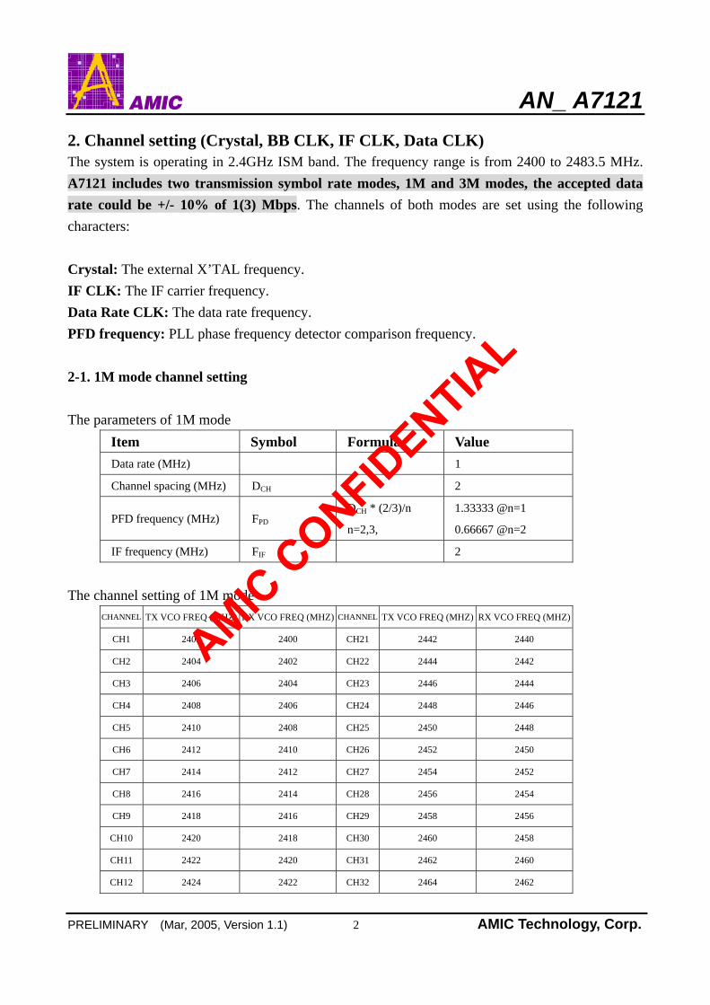
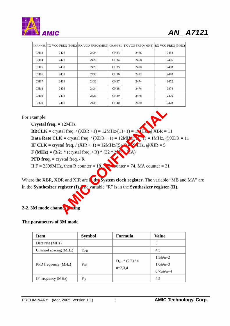
2. Channel setting (Crystal, BB CLK, IF CLK, Data CLK) The system is operating in 2.4GHz ISM band. The frequency range is from 2400 to 2483.5 MHz. A7121 includes two transmission symbol rate modes, 1M and 3M modes, the accepted data rate could be +/- 10% of 1(3) Mbps. The channels of both modes are set using the following characters: Crystal: The external X’TAL frequency. IF CLK: The IF carrier frequency. Data Rate CLK: The data rate frequency. PFD frequency: PLL phase frequency detector comparison frequency. 2-1. 1M mode channel setting The parameters of 1M mode
Item Symbol Formula Value Data rate (MHz) 1
Channel spacing (MHz) DCH 2
PFD frequency (MHz) FPD DCH * (2/3)/n
n=2,3,
1.33333 @n=1
0.66667 @n=2
IF frequency (MHz) FIF 2
The channel setting of 1M mode
CHANNEL TX VCO FREQ (MHZ) RX VCO FREQ (MHZ) CHANNEL TX VCO FREQ (MHZ) RX VCO FREQ (MHZ)
CH1 2402 2400 CH21 2442 2440
CH2 2404 2402 CH22 2444 2442
CH3 2406 2404 CH23 2446 2444
CH4 2408 2406 CH24 2448 2446
CH5 2410 2408 CH25 2450 2448
CH6 2412 2410 CH26 2452 2450
CH7 2414 2412 CH27 2454 2452
CH8 2416 2414 CH28 2456 2454
CH9 2418 2416 CH29 2458 2456
CH10 2420 2418 CH30 2460 2458
CH11 2422 2420 CH31 2462 2460
CH12 2424 2422 CH32 2464 2462
AM
IC C
ONFID
ENTIA
L
AN_ A7121
PRELIMINARY (Mar, 2005, Version 1.1) 3 AMIC Technology, Corp.
CHANNEL TX VCO FREQ (MHZ) RX VCO FREQ (MHZ) CHANNEL TX VCO FREQ (MHZ) RX VCO FREQ (MHZ)
CH13 2426 2424 CH33 2466 2464
CH14 2428 2426 CH34 2468 2466
CH15 2430 2428 CH35 2470 2468
CH16 2432 2430 CH36 2472 2470
CH17 2434 2432 CH37 2474 2472
CH18 2436 2434 CH38 2476 2474
CH19 2438 2426 CH39 2478 2476
CH20 2440 2438 CH40 2480 2478
For example:
Crystal freq. = 12MHz BBCLK = crystal freq. / (XBR +1) = 12MHz/(11+1) = 1MHz, @XBR = 11
Data Rate CLK = crystal freq. / (XDR + 1) = 12MHz/(11+1) = 1MHz, @XDR = 11 IF CLK = crystal freq. / (XIR + 1) = 12MHz/(5+1) = 2MHz, @XIR = 5 F (MHz) = (3/2) * (crystal freq. / R) * (32 * MB + MA) PFD freq. = crystal freq. / R If F = 2399MHz, then R counter = 18, MB counter = 74, MA counter = 31 Where the XBR, XDR and XIR are in the System clock register. The variable “MB and MA” are in the Synthesizer register (I). The variable “R” is in the Synthesizer register (II). 2-2. 3M mode channel setting The parameters of 3M mode
Item Symbol Formula Value Data rate (MHz) 3
Channel spacing (MHz) DCH 4.5
PFD frequency (MHz) FPD DCH * (2/3) / n
n=2,3,4
1.5@n=2
1.0@n=3
0.75@n=4
IF frequency (MHz) FIF 4.5
AM
IC C
ONFID
ENTIA
L
AN_ A7121
PRELIMINARY (Mar, 2005, Version 1.1) 4 AMIC Technology, Corp.
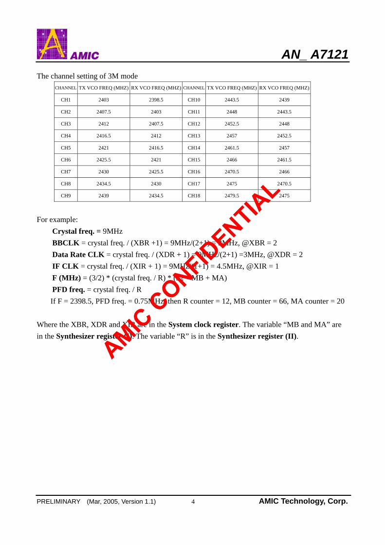
The channel setting of 3M mode CHANNEL TX VCO FREQ (MHZ) RX VCO FREQ (MHZ) CHANNEL TX VCO FREQ (MHZ) RX VCO FREQ (MHZ)
CH1 2403 2398.5 CH10 2443.5 2439
CH2 2407.5 2403 CH11 2448 2443.5
CH3 2412 2407.5 CH12 2452.5 2448
CH4 2416.5 2412 CH13 2457 2452.5
CH5 2421 2416.5 CH14 2461.5 2457
CH6 2425.5 2421 CH15 2466 2461.5
CH7 2430 2425.5 CH16 2470.5 2466
CH8 2434.5 2430 CH17 2475 2470.5
CH9 2439 2434.5 CH18 2479.5 2475
For example:
Crystal freq. = 9MHz BBCLK = crystal freq. / (XBR +1) = 9MHz/(2+1) = 3MHz, @XBR = 2 Data Rate CLK = crystal freq. / (XDR + 1) = 9MHz/(2+1) =3MHz, @XDR = 2 IF CLK = crystal freq. / (XIR + 1) = 9MHz/(1+1) = 4.5MHz, @XIR = 1
F (MHz) = (3/2) * (crystal freq. / R) * (32 * MB + MA) PFD freq. = crystal freq. / R
If F = 2398.5, PFD freq. = 0.75MHz, then R counter = 12, MB counter = 66, MA counter = 20 Where the XBR, XDR and XIR are in the System clock register. The variable “MB and MA” are in the Synthesizer register (I). The variable “R” is in the Synthesizer register (II).
AM
IC C
ONFID
ENTIA
L
AN_ A7121
PRELIMINARY (Mar, 2005, Version 1.1) 5 AMIC Technology, Corp.
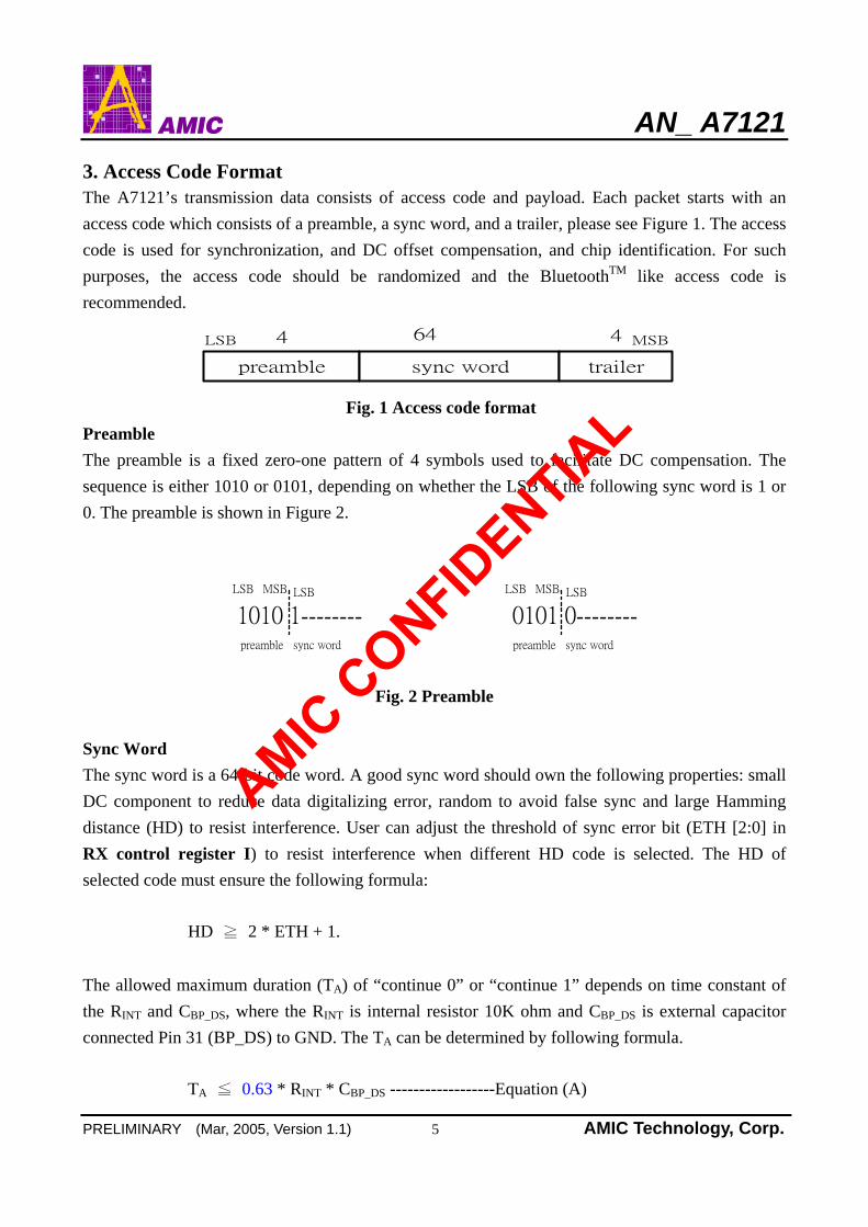
3. Access Code Format The A7121’s transmission data consists of access code and payload. Each packet starts with an access code which consists of a preamble, a sync word, and a trailer, please see Figure 1. The access code is used for synchronization, and DC offset compensation, and chip identification. For such purposes, the access code should be randomized and the BluetoothTM like access code is recommended.
preamble sync word trailer
LSB MSB4 64 4
Fig. 1 Access code format Preamble The preamble is a fixed zero-one pattern of 4 symbols used to facilitate DC compensation. The sequence is either 1010 or 0101, depending on whether the LSB of the following sync word is 1 or 0. The preamble is shown in Figure 2.
1010 1--------LSB MSB LSB
preamble sync word
0101 0--------LSB MSB LSB
preamble sync word
Fig. 2 Preamble
Sync Word The sync word is a 64-bit code word. A good sync word should own the following properties: small DC component to reduce data digitalizing error, random to avoid false sync and large Hamming distance (HD) to resist interference. User can adjust the threshold of sync error bit (ETH [2:0] in RX control register I) to resist interference when different HD code is selected. The HD of selected code must ensure the following formula:
HD ≧ 2 * ETH + 1.
The allowed maximum duration (TA) of “continue 0” or “continue 1” depends on time constant of the RINT and CBP_DS, where the RINT is internal resistor 10K ohm and CBP_DS is external capacitor connected Pin 31 (BP_DS) to GND. The TA can be determined by following formula.
TA ≦ 0.63 * RINT * CBP_DS ------------------Equation (A)
AM
IC C
ONFID
ENTIA
L
AN_ A7121
PRELIMINARY (Mar, 2005, Version 1.1) 6 AMIC Technology, Corp.
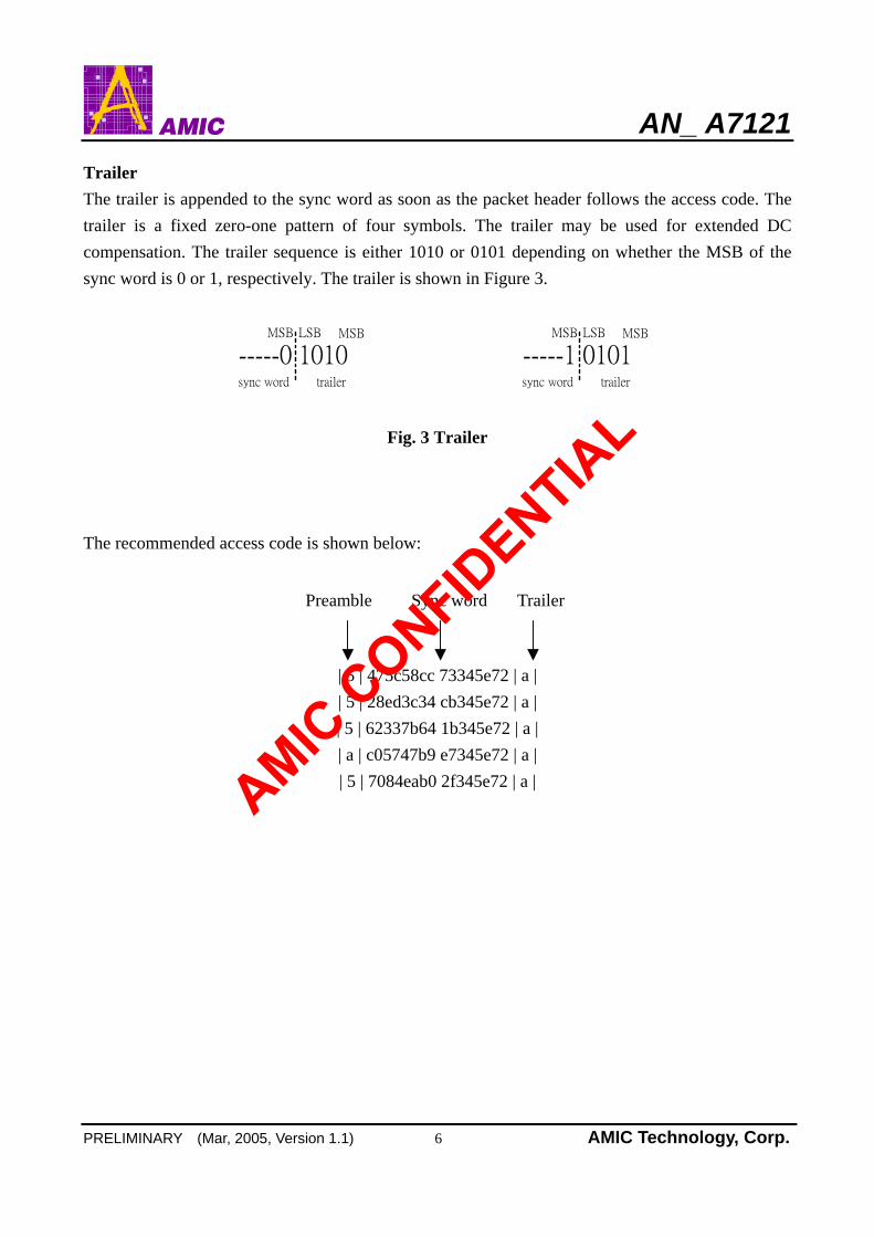
Trailer The trailer is appended to the sync word as soon as the packet header follows the access code. The trailer is a fixed zero-one pattern of four symbols. The trailer may be used for extended DC compensation. The trailer sequence is either 1010 or 0101 depending on whether the MSB of the sync word is 0 or 1, respectively. The trailer is shown in Figure 3.
-----0 1010LSB MSBMSB
trailersync word
-----1 0101LSB MSBMSB
trailersync word
Fig. 3 Trailer
The recommended access code is shown below:
| 5 | 475c58cc 73345e72 | a | | 5 | 28ed3c34 cb345e72 | a | | 5 | 62337b64 1b345e72 | a | | a | c05747b9 e7345e72 | a | | 5 | 7084eab0 2f345e72 | a |
Preamble Sync word Trailer
AM
IC C
ONFID
ENTIA
L
AN_ A7121
PRELIMINARY (Mar, 2005, Version 1.1) 7 AMIC Technology, Corp.
4. TX power control setting TX power control can be set by TX control register (I) and (II). For general application, the TX output power range is 6dB (i.e. TX output power is 0, -3 and –6 dBm). The power range can be extended to 10dB by setting the IQC [1:0] register. The following is recommended setting value of TX power. IA [4:0]: I amplitude fine tuning. Recommend value= 11111. QA [4:0]: Q amplitude fine tuning. Recommend value= 11111. IO [3:0]: I offset tuning. Recommend value= 1000. QO [3:0]: Q offset tuning. Recommend value= 1000. PC [5:0]: TX power control. IQC [1:0]: IQ amplitude course tuning. 4-1. TX output power = 0dBm
PC [5:0]: setting value = 111111. IQC [1:0]: setting value = 11.
4-2. TX output power = -3dBm PC [5:0]: setting value = 000111. IQC [1:0]: setting value = 11.
4-3. TX output power = -6dBm PC [5:0]: setting value = 000000. IQC [1:0]: setting value = 11.
4-4. TX output power = -10dBm PC [5:0]: setting value = 000000. IQC [1:0]: setting value = 10.
AM
IC C
ONFID
ENTIA
L
AN_ A7121
PRELIMINARY (Mar, 2005, Version 1.1) 8 AMIC Technology, Corp.
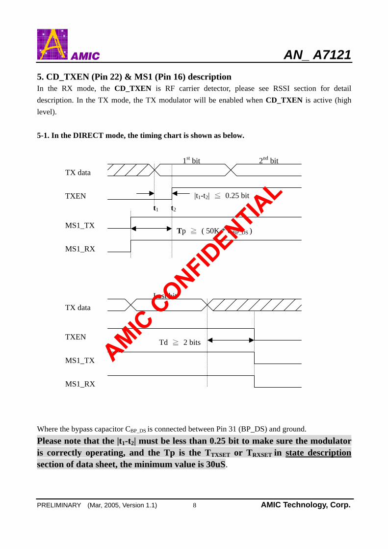
5. CD_TXEN (Pin 22) & MS1 (Pin 16) description In the RX mode, the CD_TXEN is RF carrier detector, please see RSSI section for detail description. In the TX mode, the TX modulator will be enabled when CD_TXEN is active (high level). 5-1. In the DIRECT mode, the timing chart is shown as below. Where the bypass capacitor CBP_DS is connected between Pin 31 (BP_DS) and ground. Please note that the |t1-t2| must be less than 0.25 bit to make sure the modulator is correctly operating, and the Tp is the TTXSET or TRXSET in state description section of data sheet, the minimum value is 30uS.
Last bit TX data
TXEN
MS1_TX
Td ≧ 2 bits
MS1_RX
MS1_TX
MS1_RX
Tp ≧ ( 50K * CBP_DS )
t1 t2
TXEN
TX data 2nd bit 1st bit
|t1-t2| ≦ 0.25 bit
AM
IC C
ONFID
ENTIA
L
AN_ A7121
PRELIMINARY (Mar, 2005, Version 1.1) 9 AMIC Technology, Corp.
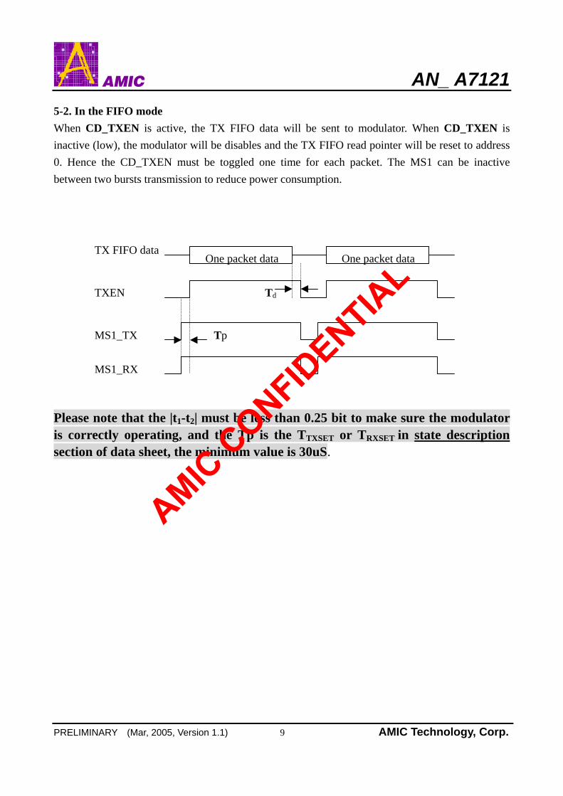
5-2. In the FIFO mode When CD_TXEN is active, the TX FIFO data will be sent to modulator. When CD_TXEN is inactive (low), the modulator will be disables and the TX FIFO read pointer will be reset to address 0. Hence the CD_TXEN must be toggled one time for each packet. The MS1 can be inactive between two bursts transmission to reduce power consumption. Please note that the |t1-t2| must be less than 0.25 bit to make sure the modulator is correctly operating, and the Tp is the TTXSET or TRXSET in state description section of data sheet, the minimum value is 30uS.
TXEN
TX FIFO data One packet data One packet data
Td
MS1_TX
MS1_RX
Tp
AM
IC C
ONFID
ENTIA
L
AN_ A7121
PRELIMINARY (Mar, 2005, Version 1.1) 10 AMIC Technology, Corp.
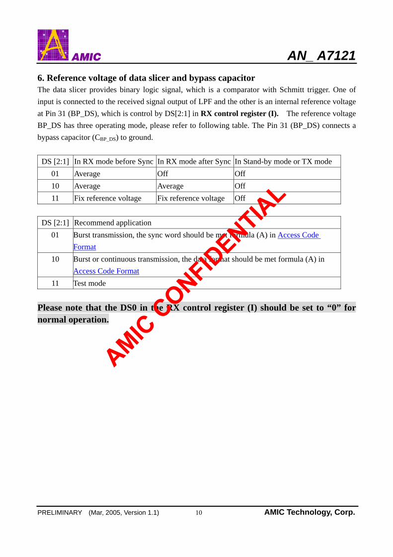
6. Reference voltage of data slicer and bypass capacitor The data slicer provides binary logic signal, which is a comparator with Schmitt trigger. One of input is connected to the received signal output of LPF and the other is an internal reference voltage at Pin 31 (BP_DS), which is control by DS[2:1] in RX control register (I). The reference voltage BP_DS has three operating mode, please refer to following table. The Pin 31 (BP_DS) connects a bypass capacitor (CBP_DS) to ground.
DS [2:1] In RX mode before Sync In RX mode after Sync In Stand-by mode or TX mode 01 Average Off Off 10 Average Average Off 11 Fix reference voltage Fix reference voltage Off
DS [2:1] Recommend application
01 Burst transmission, the sync word should be met formula (A) in Access Code Format
10 Burst or continuous transmission, the data format should be met formula (A) in Access Code Format
11 Test mode Please note that the DS0 in the RX control register (I) should be set to “0” for normal operation.
AM
IC C
ONFID
ENTIA
L

AN_ A7121
PRELIMINARY (Mar, 2005, Version 1.1) 11 AMIC Technology, Corp.
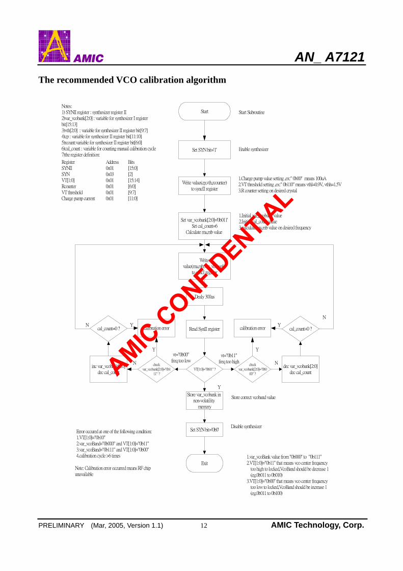
7. VCO Band Calibration The A7121 has 8 VCO bands (from band 0 to band 7) that are set in Synthesizer register I. The relationship between VCO band and frequency is shown below. To make sure VCO is operating in suitable band, VCO calibration must be done in chip initialization and its algorithm is shown below.
VCO Band
2.25
2.30
2.35
2.40
2.45
2.50
2.55
2.60
2.65
2.70
0.0 0.2 0.4 0.6 0.8 1.0 1.2 1.4 1.6 1.8 2.0 2.2 2.4 2.6
VT (volt)
Fre
quen
cy (
GH
z)
Band 0
Band 1
Band 2
Band 3
Band 4
Band 5
Band 6
Band 7
AM
IC C
ONFID
ENTIA
L
AN_ A7121
PRELIMINARY (Mar, 2005, Version 1.1) 12 AMIC Technology, Corp.
The recommended VCO calibration algorithm
Start
Set SYN bit='1'
Set var_vcobank[2:0]='0b011'Set cal_count=6
Calculate ma,mb value
Dealy 300us
VT[1:0]="0b01" ?check
var_vcobank[2:0]="0b111" ?
checkvar_vcobank[2:0]="0b0
00" ?
Set SYN bit='0b0'
Exit
dec var_vcobank[2:0]dec cal_count
cal_count=0 ?
inc var_vcobank[2:0]dec cal_count
cal_count=0 ?
vt="0b11"freq too high
vt="0b00"freq too low
Y
N
calibration error
N
Ycalibration error
YY
YN
Start Subroutine
1.var_vcoBank value from "0b000" to "0b111"2.VT[1:0]="0b11" that means vco center frequency
too high to locked,VcoBand should be decrease 1 (eg.0b011 to 0b010)
3.VT[1:0]="0b00" that means vco center frequency too low to locked,VcoBand should be increase 1 (eg.0b011 to 0b100)
Error occured at one of the following condition:1.VT[1:0]="0b10"2.var_vcoBand="0b000" and VT[1:0]="0b11"3.var_vcoBand="0b111" and VT[1:0]="0b00"4.calibration cycle >6 times
Notes: 1) SYNII register : synthesizer register II2)var_vcobank[2:0] : variable for synthesizer I register bit[15:13]3)vth[2:0] : variable for synthesizer II register bit[9:7]4)cp : variable for synthesizer II register bit[11:10]5)rcount:variable for synthesizer II register bit[6:0] 6)cal_count : variable for counting manual calibration cycle7)the register definition:
Write value(cp,vth,rcounter)to syncII register
Write value(ma,mb,var_vcobank)
to syncI register
Read SynII register
Store var_vcobank in non-volatility
memory
Enable synthesizer
1.Charge pump value setting ,ex:" 0b00" means 100uA2.VT threshold setting ,ex:" 0b110" means vthl=0.9V, vthh=1.5V3.R counter setting on desired crystal
1.Initial var_vcobank value2.Initial cal_count value3.calculate ma,mb value on desired frequency
Store correct vcoband value
Disable synthesizer
Register Address BitsSYNII 0x01 [15:0]SYN 0x03 [2]VT[1:0] 0x01 [15:14]Rcounter 0x01 [6:0]VT threshold 0x01 [9:7]Charge pump current 0x01 [11:0]
N
Note: Calibration error occurred means RF chip unavailable
AM
IC C
ONFID
ENTIA
L
AN_ A7121
PRELIMINARY (Mar, 2005, Version 1.1) 13 AMIC Technology, Corp.
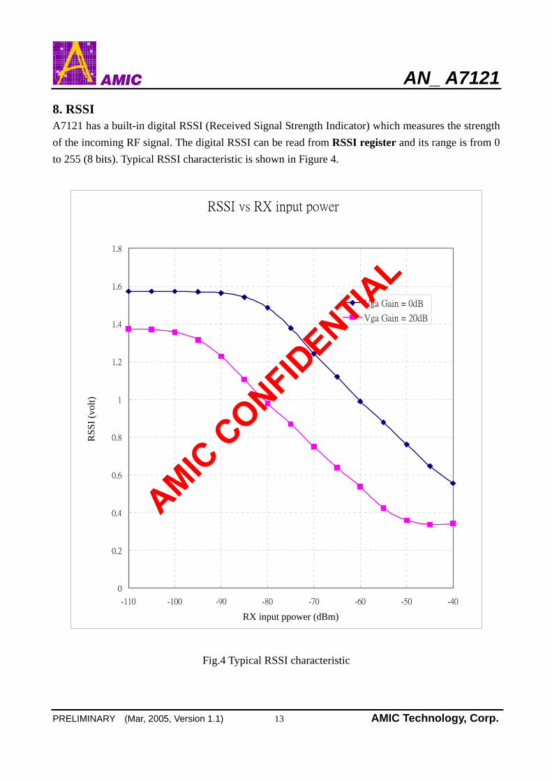
8. RSSI A7121 has a built-in digital RSSI (Received Signal Strength Indicator) which measures the strength of the incoming RF signal. The digital RSSI can be read from RSSI register and its range is from 0 to 255 (8 bits). Typical RSSI characteristic is shown in Figure 4.
RSSI vs RX input power
0
0.2
0.4
0.6
0.8
1
1.2
1.4
1.6
1.8
-110 -100 -90 -80 -70 -60 -50 -40
RX input ppower (dBm)
RSS
I (vo
lt)
Vga Gain = 0dB
Vga Gain = 20dB
Fig.4 Typical RSSI characteristic
AM
IC C
ONFID
ENTIA
L
AN_ A7121
PRELIMINARY (Mar, 2005, Version 1.1) 14 AMIC Technology, Corp.
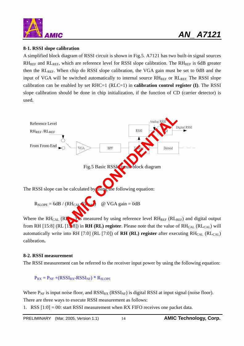
8-1. RSSI slope calibration A simplified block diagram of RSSI circuit is shown in Fig.5. A7121 has two built-in signal sources RHREF and RLREF, which are reference level for RSSI slope calibration. The RHREF is 6dB greater then the RLREF. When chip do RSSI slope calibration, the VGA gain must be set to 0dB and the input of VGA will be switched automatically to internal source RHREF or RLREF. The RSSI slope calibration can be enabled by set RHC=1 (RLC=1) in calibration control register (I). The RSSI slope calibration should be done in chip initialization, if the function of CD (carrier detector) is used.
VGA BPF Limiter Demod
A/DDigital RSSI
RSSI
Analog RSSI
Fig.5 Basic RSSI circuit block diagram The RSSI slope can be calculated by using the following equation:
RSLOPE = 6dB / (RHCAL-RLCAL) @ VGA gain = 0dB
Where the RHCAL (RLCAL) is measured by using reference level RHREF (RLREF) and digital output from RH [15:8] (RL [15:8]) in RH (RL) register. Please note that the value of RHCAL (RLCAL) will automatically write into RH [7:0] (RL [7:0]) of RH (RL) register after executing RHCAL (RLCAL) calibration. 8-2. RSSI measurement The RSSI measurement can be referred to the receiver input power by using the following equation:
PRX = PNF +(RSSIRX-RSSINF) * RSLOPE
Where PNF is input noise floor, and RSSIRX (RSSINF) is digital RSSI at input signal (noise floor). There are three ways to execute RSSI measurement as follows: 1. RSS [1:0] = 00: start RSSI measurement when RX FIFO receives one packet data.
Reference Level
RHREF /RLREF
From Front-End
AM
IC C
ONFID
ENTIA
L
AN_ A7121
PRELIMINARY (Mar, 2005, Version 1.1) 15 AMIC Technology, Corp.
2. RSS [1:0] = 01: start RSSI measurement when RX sync is active. 3. RSS [1:0] = 1X: start RSSI measurement when ERSS is set to 1 (enable) on the Calibration
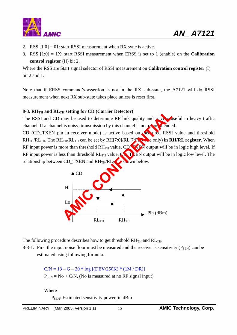
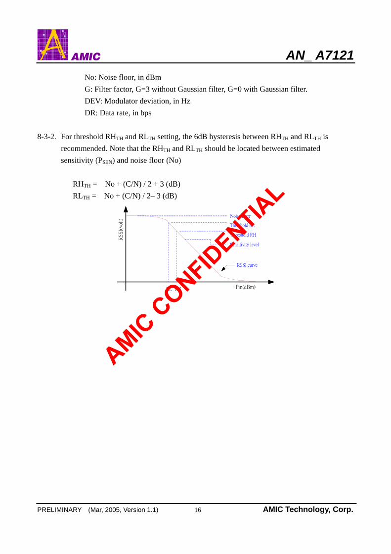
control register (II) bit 2. Where the RSS are Start signal selector of RSSI measurement on Calibration control register (I) bit 2 and 1. Note that if ERSS command’s assertion is not in the RX sub-state, the A7121 will do RSSI measurement when next RX sub-state takes place unless is reset first. 8-3. RHTH and RLTH setting for CD (Carrier Detector) The RSSI and CD may be used to determine RF link quality and is very useful in heavy traffic channel. If a channel is noisy, transmission by this channel is not recommended. CD (CD_TXEN pin in receiver mode) is active based on measured RSSI value and threshold RHTH/RLTH. The RHTH/RLTH can be set by RH[7:0]/RL[7:0] (write only) in RH/RL register. When RF input power is more than threshold RHTH value, CD_TXEN output will be in logic high level. If RF input power is less than threshold RLTH value, CD_TXEN output will be in logic low level. The relationship between CD_TXEN and RHTH/RLTH is shown below. The following procedure describes how to get threshold RHTH and RLTH. 8-3-1. First the input noise floor must be measured and the receiver’s sensitivity (PSEN) can be
estimated using following formula. C/N = 13 – G – 20 * log [(DEV/250K) * (1M / DR)] PSEN = No + C/N, (No is measured at no RF signal input) Where
PSEN: Estimated sensitivity power, in dBm
Pin (dBm)
CD
RLTH RHTH
Hi
Lo
AM
IC C
ONFID
ENTIA
L
AN_ A7121
PRELIMINARY (Mar, 2005, Version 1.1) 16 AMIC Technology, Corp.
No: Noise floor, in dBm G: Filter factor, G=3 without Gaussian filter, G=0 with Gaussian filter. DEV: Modulator deviation, in Hz DR: Data rate, in bps
8-3-2. For threshold RHTH and RLTH setting, the 6dB hysteresis between RHTH and RLTH is
recommended. Note that the RHTH and RLTH should be located between estimated sensitivity (PSEN) and noise floor (No)
RHTH = No + (C/N) / 2 + 3 (dB) RLTH = No + (C/N) / 2– 3 (dB)
Noise floor
Threshold RL
Threshold RH
Sensitivity level
RS
SI(
volt
)
RSSI curve
Pin(dBm)RL RH
AM
IC C
ONFID
ENTIA
L
AN_ A7121
PRELIMINARY (Mar, 2005, Version 1.1) 17 AMIC Technology, Corp.
The recommended RSSI slope calibration algorithm
Disable synthesizer
Set auto calibration item 1)select RHC,RLC 2)select auto calibration status
Enable calibration start
Note:If error flag occured , repeat this flow or RF chip is unavailable
Set VGA gain = 0dB
1.Set ADC sampling clock value ,suggest value '0b0011'2.Set BPF, LPF measurement clock delay, suggest value '0b011'3.Set RH, RL calibration clock delay, suggest value '0b011'
Start
Set VGA[2:0]='0b0XX'
Set SYN bit = '0b0'
Set ECAL bit ='0b1'
RHR & RLR bit ='0b1' ?
Exit
Calculate RSSI slop
Y
Start Subroutine
Set ADC[3:0]='0b0011'Set AD[5:3]='0b011'Set AD[8:6]='0b011'
Set RHC & RLC bit = '0b1'Set MCAL bit = '0b0'
Get RH, RL value for calculate RSSI slope
1.Readout RH value in the RH register2.Readout RL value in the RL register
Calculate RSSI solpe and store value in non-volatility memory
Note:1.T_CNT : variable for timeout count2.X is constant for timeout, suggest minimum timeout vlaue 100us3.The register definition:Register Address BitsVGA 0x07 [2:0]ADC 0x0E [3:0]AD 0x0E [12:4]SYN 0x03 [2]RHC 0x0C [7]RLC 0x0C [8]MCAL 0x0C [3]ECAL 0x0D [1]RHR 0x0C [10]RLR 0x0C [9]RH 0x12 [15:8]RL 0x13 [15:8]
Set error flag
Read RHR,RLR bit
T_CNT>X ?
Y
N
N
Read RHR & RLR bit
T_CNT++
AM
IC C
ONFID
ENTIA
L
AN_ A7121
PRELIMINARY (Mar, 2005, Version 1.1) 18 AMIC Technology, Corp.
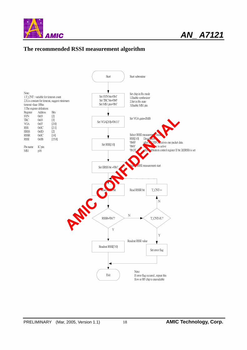
The recommended RSSI measurement algorithm
Start
Set RSS[1:0]
Set error flag
RSSR='0b1'?
Exit
Y
Start subroutine
Set ERSS bit ='0b1'
Readout RSSI[7:0]
Select RSSI measurement modeRSS[1:0] Description'0b00' after RX FIFO receives one packet data'0b01' after RX sync is active'0b1X' after calibration control register II bit 2(ERSS) is set
Enable RSSI measurement start
Readout RSSI value
Set VGA[2:0]='0b111'
Set SYN bit='0b1'Set TRC bit='0b0'Set MS1 pin='0b1'
Set VGA gain=20dB
Set chip in Rx mode1.Enable synthesizer2.Set in Rx state3.Enable MS1 pin
Note:1.T_CNT : variable for timeout count2.X is constant for timeout, suggest minimum timeout vlaue 100us3.The register definition:Register Address BitsSYN 0x03 [2]TRC 0x03 [3]VGA 0x07 [2:0]RSS 0x0C [2:1]ERSS 0x0D [2]RSSR 0x0C [14]RSSI 0x0B [15:8]
Pin name IC pinMS1 p16
Note:If error flag occured , repeat this flow or RF chip is unavailable
Read RSSR bit
NT_CNT>X ?
Y
N
Read RSSR bit T_CNT++
AM
IC C
ONFID
ENTIA
L

AN_ A7121
PRELIMINARY (Mar, 2005, Version 1.1) 19 AMIC Technology, Corp.
9. Data transmission mode A7121 has two data transmission mode, DIRECT mode and FIFO mode. In DIRECT mode, the transceiver can communicate at a high data rate of 1 or 3 Mbps for maximum data throughput performance. For all low data rate applications, FIFO mode enables the on-chip FIFO to clock in data at a low data rate from a low speed micro-controller and transmit at high data rate of 1 or 3 Mbps. 9-1. DIRECT mode In DIRECT mode, there is no buffer between data and modulation (demodulation) circuit. The TX data must be synchronized with chip’s system clock (crystal frequency). All transmission access code (preamble, sync word and data) must be implemented in base-band or firmware. In this mode, the TX & RX FIFO is disabled, please see table below. Where the EFW and EFR are in the FIFO control register, and DPC [1:0] is in the RX control register (I).
Mode EFW EFR DPC [1:0] Remark
00 Disable frame sync and FIFO. No data process at RX data output.
01 Enable frame sync and disable FIFO. RX data output is inactive (high) before sync.
DIRECT 0 0
10 Enable frame sync and disable FIFO. No data process at RX data output.
FIFO X X 11 Enable frame sync and FIFO. The setting of EFW & EFR, please refer to section 9-2
For the setting of data input and output, please see table below, the TRD bit is in Mode control register.
TRD TX input port RX output port Remark
1 Pin 21 (TRXD) Pin 21 (TRXD) Pin 21 is bi-directional, and Pin 20 is disabled.
0 Pin 20 (TXD) Pin 21 (TRXD) Pin 21 is output port only.
AM
IC C
ONFID
ENTIA
L
AN_ A7121
PRELIMINARY (Mar, 2005, Version 1.1) 20 AMIC Technology, Corp.
In receiver side, frame synchronization is available and enabled by DPC [1:0]. If this function is used, the RX access code should be written into Access code register before the chip enters RX sub-state. Once the frame is synchronized, the sync signal (Pin 23) is active with RX data sampling clock (Pin 24) accompanied. Please note that the RX data sampling clock is not a true recovered clock. Hence, if the chip needs to communicate continuously, an external clock recovery circuit must be implemented. For burst transmission, if RX data sampling clock is used, the maximum payload length (BMAX) is recommend by following formula.
BMAX = 1 / [10 * (FTOLTX - FTOLRX)], bit = 2500 bit @ FTOLTX = FTOLRX = +/-20ppm
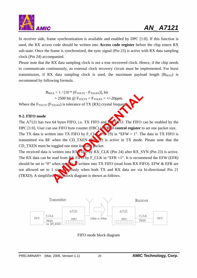
Where the FTOLTX (FTOLRX) is tolerance of TX (RX) crystal frequency. 9-2. FIFO mode The A7121 has two 64 bytes FIFO, i.e. TX FIFO and RX FIFO. The FIFO can be enabled by the DPC [1:0]. User can use FIFO byte counter (FBC) in FIFO control register to set one packet size. The TX data is written into TX FIFO by F_CLK (Pin 19) in “EFW = 1”. The data in TX FIFO is transmitted via RF when the CD_TXEN (Pin 22) is active in TX mode. Please note that the CD_TXEN must be toggled one time for each packet. The received data is written into RX FIFO by RX_CLK (Pin 24) after RX_SYN (Pin 23) is active. The RX data can be read from RX FIFO by F_CLK in “EFR =1”. It is recommend the EFW (EFR) should be set to “0” when no data is written into TX FIFO (read from RX FIFO). EFW & EFR are not allowed set to 1 simultaneously when both TX and RX data are via bi-directional Pin 21 (TRXD). A simplified FIFO block diagram is shown as follows.
MCU MCUFIFO
A7121
F_CLK
TRXD(or SPI_RXD)
Transmitter Receiver
F_CLK
TRXD1Mbps or 3MbpsFIFO
A7121
FIFO mode block diagram
AM
IC C
ONFID
ENTIA
L
AN_ A7121
PRELIMINARY (Mar, 2005, Version 1.1) 21 AMIC Technology, Corp.
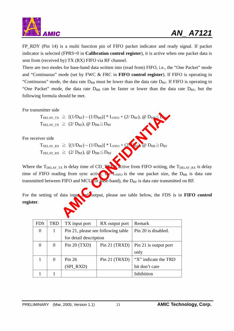
FP_RDY (Pin 14) is a multi function pin of FIFO packet indicator and ready signal. If packet indicator is selected (FPRS=0 in Calibration control register), it is active when one packet data is sent from (received by) TX (RX) FIFO via RF channel. There are two modes for base-band data written into (read from) FIFO, i.e., the “One Packet” mode and “Continuous” mode (set by FWC & FRC in FIFO control register). If FIFO is operating in “Continuous” mode, the data rate DBB must be lower than the data rate DRF. If FIFO is operating in “One Packet” mode, the data rate DBB can be faster or lower than the data rate DRF, but the following formula should be met. For transmitter side
TDELAY_TX ≧ [(1/DRF) – (1/DBB)] * LFIFO + (2/ DRF), @ DBB≦DRF TDELAY_TX ≧ (2/ DRF), @ DBB≧DRF
For receiver side
TDELAY_RX ≧ [(1/DRF) – (1/DBB)] * LFIFO + (2/ DRF), @ DBB≧DRF TDELAY_RX ≧ (2/ DRF), @ DBB≦DRF
Where the TDELAY_TX is delay time of CD_TXEN active from FIFO writing, the TDELAY_RX is delay time of FIFO reading from sync active, the LFIFO is the one packet size, the DBB is data rate transmitted between FIFO and MCU (or base-band), the DRF is data rate transmitted on RF. For the setting of data input and output, please see table below, the FDS is in FIFO control register.
FDS TRD TX input port RX output port Remark 0 1 Pin 21, please see following table
for detail description Pin 20 is disabled.
0 0 Pin 20 (TXD) Pin 21 (TRXD) Pin 21 is output port only
1 0 Pin 26 (SPI_RXD)
Pin 21 (TRXD) “X” indicate the TRD bit don’t care
1 1 Inhibition
AM
IC C
ONFID
ENTIA
L
AN_ A7121
PRELIMINARY (Mar, 2005, Version 1.1) 22 AMIC Technology, Corp.
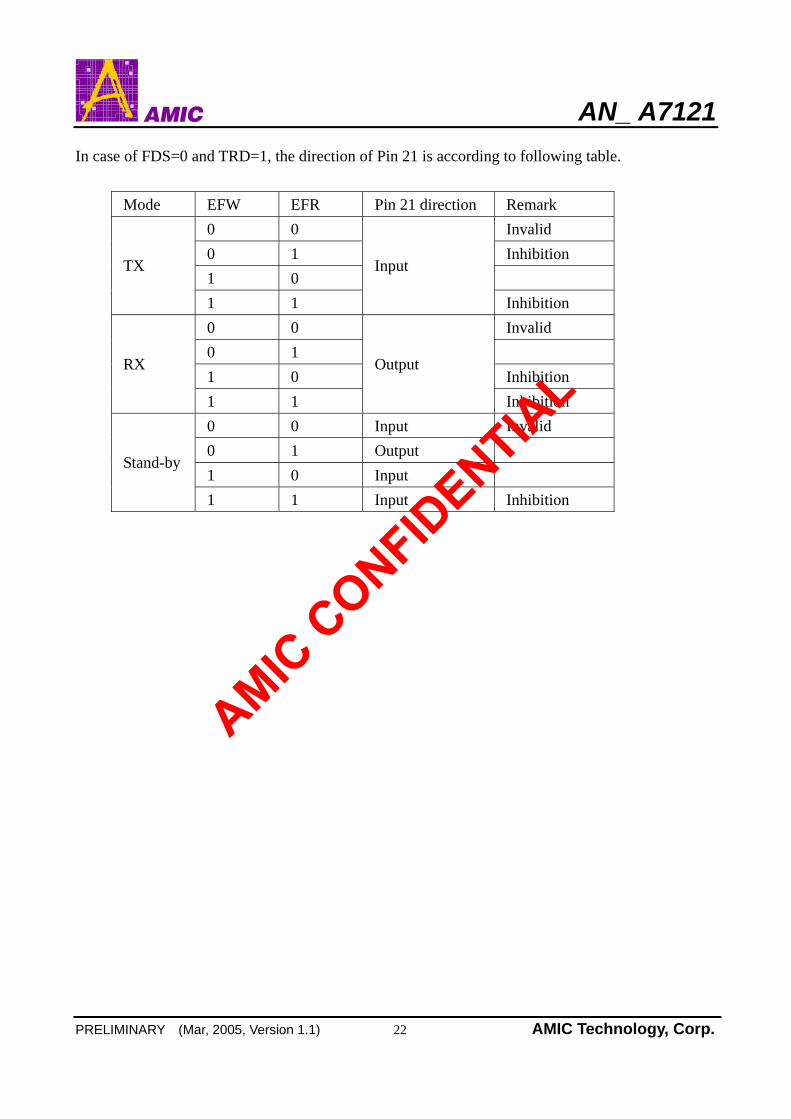
In case of FDS=0 and TRD=1, the direction of Pin 21 is according to following table.
Mode EFW EFR Pin 21 direction Remark 0 0 Invalid 0 1 Inhibition 1 0
TX
1 1
Input
Inhibition 0 0 Invalid 0 1 1 0 Inhibition
RX
1 1
Output
Inhibition 0 0 Input Invalid 0 1 Output 1 0 Input
Stand-by
1 1 Input Inhibition
AM
IC C
ONFID
ENTIA
L
AN_ A7121
PRELIMINARY (Mar, 2005, Version 1.1) 23 AMIC Technology, Corp.
The recommended algorithm for FIFO mode transmitter
Set FIFO control register1)select input data pin TXD or SPI_RXD 2)set FCLKI is normal state3)enable Tx FIFO write4)set one package write5)set desired FIFO bytes number
Set calibration control register1)set FIFO package ready state2)set FP_RDY signal is normal
Load data to FIFO
Start to transmit data
Disable FIFO write
Start
Set FDS bit='0b0'Set FCKI bit='0b0'Set EFW bit ='0b1'Set FWC bit='0b0'
Set FBC[5:0]='0b111111'
Using TXD ,F_CLK pin write data to FIFO
FP_RDY=1 ?
Exit
Y
Start Subroutine
Set FPRS bit='0b0'Set FPRI bit='0b0'
Enable CD_TXEN pin
Set EFW bit='0b0'
Set DPC[1:0]='0b11'Enable frame sync and FIFO
Delay 10usDelay
1.The register definition:Register Address BitsDPC 0x06 [2:1]FDS 0x08 [0]FCKI 0x08 [1]EFW 0x08 [2]FWC 0x08 [3]FBC 0x08 [11:6]FPRS 0x0D [3]FPRI 0x0D [4]
Pin name IC pinFP_RDY p14F_CLK p19TXD p20
Note:1.Using F_CLK and TXD pin refer to FIFO timing of A7121 data sheet for detailed information on timing chart.
transmit time ending ?
N
Y
N
AM
IC C
ONFID
ENTIA
L
AN_ A7121
PRELIMINARY (Mar, 2005, Version 1.1) 24 AMIC Technology, Corp.
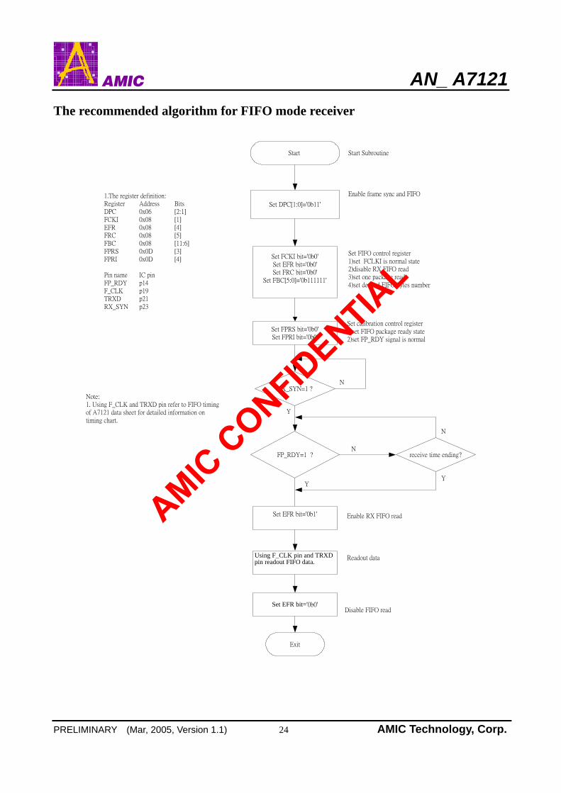
The recommended algorithm for FIFO mode receiver
Set FIFO control register1)set FCLKI is normal state2)disable RX FIFO read3)set one package read4)set desired FIFO bytes number
Set calibration control register1)set FIFO package ready state2)set FP_RDY signal is normal
Readout data
Start
Set FCKI bit='0b0'Set EFR bit='0b0'Set FRC bit='0b0'
Set FBC[5:0]='0b111111'
FP_RDY=1 ?
Exit
Y
N
Start Subroutine
Set FPRS bit='0b0'Set FPRI bit='0b0'
Using F_CLK pin and TRXDpin readout FIFO data.
Set DPC[1:0]='0b11'
Enable frame sync and FIFO
Set EFR bit='0b0'Disable FIFO read
1.The register definition:Register Address BitsDPC 0x06 [2:1]FCKI 0x08 [1]EFR 0x08 [4]FRC 0x08 [5]FBC 0x08 [11:6]FPRS 0x0D [3]FPRI 0x0D [4]
Pin name IC pinFP_RDY p14F_CLK p19TRXD p21RX_SYN p23
Note:1. Using F_CLK and TRXD pin refer to FIFO timing of A7121 data sheet for detailed information on timing chart.
receive time ending?
N
Y
Set EFR bit='0b1'
RX_SYN=1 ?
Y
N
Enable RX FIFO read
AM
IC C
ONFID
ENTIA
L
AN_ A7121
PRELIMINARY (Mar, 2005, Version 1.1) 25 AMIC Technology, Corp.
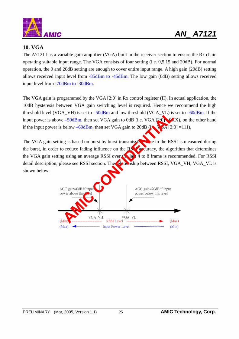
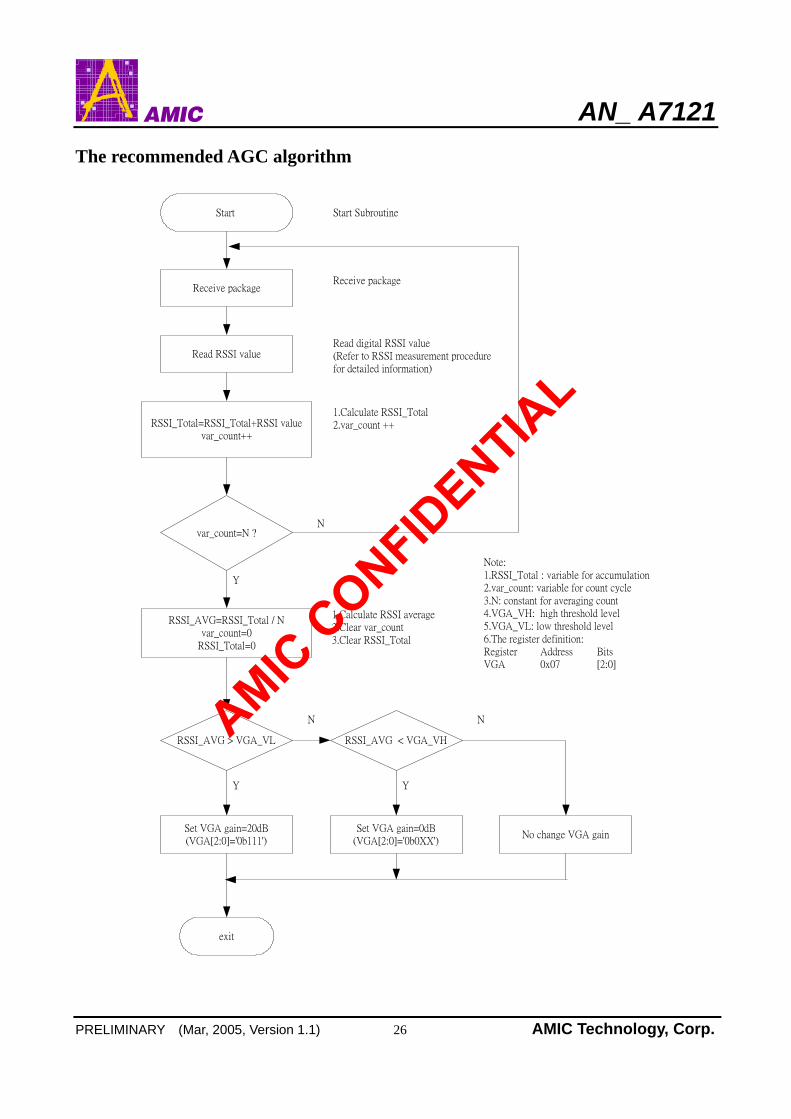
10. VGA The A7121 has a variable gain amplifier (VGA) built in the receiver section to ensure the Rx chain operating suitable input range. The VGA consists of four setting (i.e. 0,5,15 and 20dB). For normal operation, the 0 and 20dB setting are enough to cover entire input range. A high gain (20dB) setting allows received input level from -85dBm to -45dBm. The low gain (0dB) setting allows received input level from -70dBm to -30dBm. The VGA gain is programmed by the VGA [2:0] in Rx control register (II). In actual application, the 10dB hysteresis between VGA gain switching level is required. Hence we recommend the high threshold level (VGA_VH) is set to –50dBm and low threshold (VGA_VL) is set to –60dBm. If the input power is above –50dBm, then set VGA gain to 0dB (i.e. VGA [2:0] =0XX), on the other hand if the input power is below –60dBm, then set VGA gain to 20dB (i.e. VGA [2:0] =111). The VGA gain setting is based on burst by burst transmission. Due to the RSSI is measured during the burst, in order to reduce fading influence on the RSSI accuracy, the algorithm that determines the VGA gain setting using an average RSSI over the last 4 to 8 frame is recommended. For RSSI detail description, please see RSSI section. The relationship between RSSI, VGA_VH, VGA_VL is shown below:
VGA_VLVGA_VH
AGC gain=0dB if input power above this level
AGC gain=20dB if input power below this level
RSSI Level (Max)(Min)
Input Power Level(Max) (Min)
AM
IC C
ONFID
ENTIA
L
AN_ A7121
PRELIMINARY (Mar, 2005, Version 1.1) 26 AMIC Technology, Corp.
The recommended AGC algorithm
Receive package
1.Calculate RSSI average 2.Clear var_count3.Clear RSSI_Total
Start
Set VGA gain=20dB(VGA[2:0]='0b111')
RSSI_AVG > VGA_VL
exit
Start Subroutine
Set VGA gain=0dB(VGA[2:0]='0b0XX')
No change VGA gain
Read RSSI value
RSSI_Total=RSSI_Total+RSSI valuevar_count++
var_count=N ?
RSSI_AVG=RSSI_Total / Nvar_count=0
RSSI_Total=0
1.Calculate RSSI_Total2.var_count ++
Y
N
Note:1.RSSI_Total : variable for accumulation2.var_count: variable for count cycle3.N: constant for averaging count4.VGA_VH: high threshold level5.VGA_VL: low threshold level6.The register definition:Register Address BitsVGA 0x07 [2:0]
Receive package
Read digital RSSI value(Refer to RSSI measurement procedure for detailed information)
RSSI_AVG < VGA_VH
Y Y
N N
AM
IC C
ONFID
ENTIA
L