Embed Size (px)
Citation preview

APPENDIX B
I/O PROCESSOR
SERVICE MANUAL

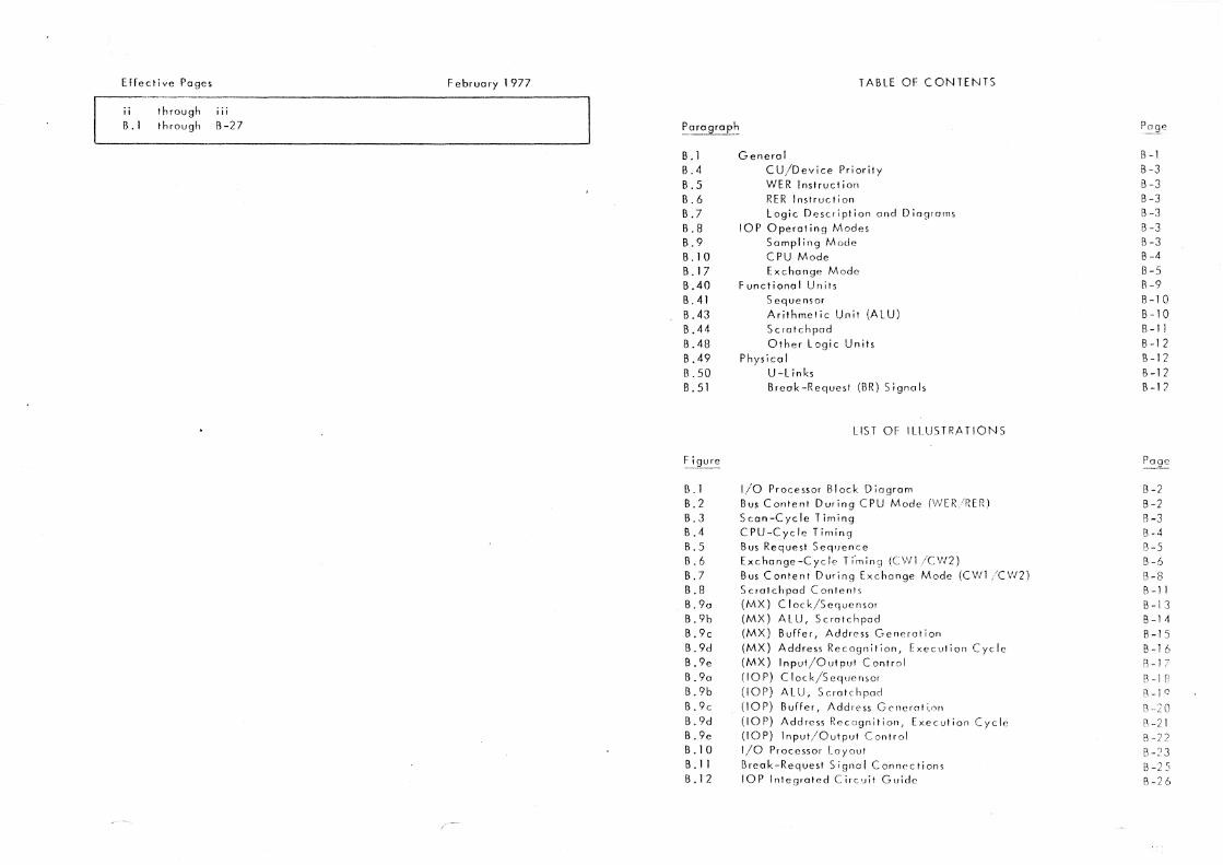
Effective Pages
ii thraugh iii B.I through B-27
February 1977
B. I B.4 B.5 B.6 B.7 B.8 B.9 B.l0 B.17 B.40 B.41 B.43 B .44 B.48 B.49 B.50 B.51
B.l B.2 B.3 B.4 B.5 B.6 B.7 B.8 B.9a B.9b B.9c B.9d B.ge
B.9a B.9b B.9c B.9d B.ge
B. 1 0 B .11 B. I 2
TABLE OF CONTENTS
General C U/D ev i ce Pri ority WER Instruction RER Instruction Logic Description and Diagrams
lOP Operating Modes Sampling Mode CPU Mode Exchange Mode
Functional Units Sequensor Arithmetic Unit (Al U)
Scratchpad Other Logic Units
Physical U -L inks Break-Request (BR) Signals
LIST OF Il.LUSTRATIONS
I/O Processor Block Diogram Bus Content During CPU Mode (I;\'Ef~ illER) Scan-Cycle Timing CPU-Cycfe Timing Bus Request Sequence Exchange-Cycle Hminq (CWI /CVl2) Bus Content During Exchonge Mode (CWI /CW2) Scrotchpad Contents (MX) C Inck/Se'luensor (MX) ,\LU, Scratchpad (MX) Buffer, Address Generotion
(MX) Address Recoqnition, Execution Cycle (MX) Input/Output Contre"
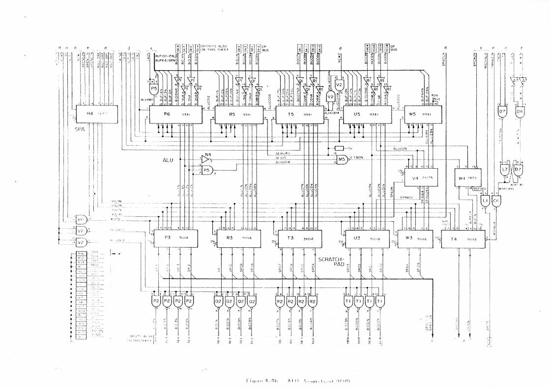
(fOP) Clock/Sequensor (lOP) ALU, Scrotchpod
(lOr) Buffer, Address Gener"t;."n (lOP) Address Recognition, Execution Cycle (lOP) Input/Output Control I/O Processor Loyout
Break-Request 5ignol Connections lOP Inteqrated C irc, .. it Guide
B-1
B-3 B-3 B-3 B-3 0-3 B-3 B -4 B-5 B -9 B 10 B-l0 B -II B-12 B -12 B -12 B -12
B-2 B-2 B-3 B -4 8-5 B-6 8-8 B -11 B-13 B-1 -1 B -15
B-16 fl-I!-
R -1 P R-IO R ··20 11-21 B-n B -:'3 B-25 B-26


APPENDIX B
I/O PROCESSOR
B.l GENERAL
The Input/Output Processor (lOP channel (Figure B-1) managE'S data transfers
directly between memory and up to E'ight multiplexed control-unit/device channels.
The lOP contains a pair of address/length control-word registers for each of its
eight channels. At the beginning of a transfer for one device, the CPU program
uses~t_",<:>_\AlE~RJI1~~tructions to load this register pair with the starting address and
the block length (Figure B-2). The lOP logic then provides all GP Bus timing
signals to control the data transfers directly between the memory and the CU.
B.2 For input or output data transfers, a CU signals that it is ready with a
Break Request (BR) to the lOP. The lOP makes a Bus Request to obtain control
of the GP Bus. The lOP then sends a simulated INR~orgTR command to the CU
to initiate one word transfer. The INR/OTR command is simulated in that it
is generated by the lOP and is not a CPU programmed instruction. The lOP
logic updates its control-word'register for each data word. When the block
length is counted down to One, the lOP sends End of ~ec,?r.d LE2.~Lto the CU
along with the lost simulated INR/OTR data transfer. The data block transfer
is ended with on SST command and status transfer between the CU and CPU.
B.3
• •
The lOP is provided in two versions:
version with cord marked MX is for P852 only .
version with cord marked lOP is for P852/856/857 .
The function and the logic .s identical for both versions. The two cords differ
in layout and in the location of components. Two sets of logic diagrams ore
thus provided to show the component locations for each version.
R I

GP BUS
GP RUS
,-_I _,i_:, '_: '~_'l_I~_;------~_-,-_'_l_(!_1J i_(,_";_"_I<_-r----II--------lI,H "I
-------~----------
L--"'_: -"-JL----~ ___ __. __ ~_.<ll:: i ." I ,-_
-
Illl)
Ii. DL:.J E J S :: ('(,'1 I T J ()tj
d
1-,I'ffLII
ADDf< [ S ') --......... __ .-;:;.;.ir,;.;.I, ____________ .I~1t\r}
f--------~--------
Bllf
IO!: flf I [Cll 01,
----------------
Bur
Figure B-1 I/O P!OCt'SSDI Block DiagrofI1
f "I'"'' ii
MAD
r-____ ~~ __ --~~._--~12~ 15
~-----L-c~T~ Address -I
I WER-2
o 4 5 8 9 12
Address
I RER
0 4 8 9
Shaded part of instructions not sent to lOP
I i "UI t: [)-2
12
CU
15
15
~
BIO
o I 2 4 15
r~f ~[T--[---~-I:-k~-:.-~--J
W~\-;;8' ~-~=~~-dd:~:~----
o
0
I not
fl, Output (memory to CU) o Input (CU to memory) 1- Word Mode o C horae tcr Mode
14 15
4 15 " T-- Block Length -----] used

B.4 CU/Device Priority
Priority of the eight CU/Device chonnels is established by the connection of the
Break RE'qu",t lines. Refer to paragroph B. 18.
B.5 WER Instruction
Two Write External Regist2r (WER) instructions (Figure B-2) are used to load the
two control words for a device into a pair of lOP registers. Bits 04, 08-15 of
the instructions are sent to the lOP on the MAD lines; bit-IS of each instruction
specifies WER-l or WER-2. The R3 field of each instruction specifies a CPU
occumulator (A I-A7) that contains the block-length or start-address control
word which is sent to the lor on the BIO lines.
8.6 RER Instruction
A single Read External Register (RER) instruction (Figure B-2) is used when the
CPU wants to test the remaining block length of on incomplete data-transfer
operation. Bits 04,08-15 of the instruction are sent to the lOP on the MAD
lines; bit IS -~ 0 a(fcesses the contral-~ord-I (block length) register in the lOP.
The R3 field of the instruction specifies the CPU accumulator (A I-A7) where the
control-word information placed on the BIO lines is to be loaded (bits 4-15).
B.7 Logic Description and Diagrams
The lOP logic is described in the sequence of its operation, in the section lor
Operating Modes. Operation of some of the more complex logic units (sequensor,
ALU, scratchpad) is given also in the section Functional Units. Logic diagrams
(Figure 1\-9, sheets a-e) ore provided at the end of the logic description. These
diagrams ore referenced on the block diagram ond in the text by the sheet number,
for example: "Ioe)ie c" refers 10 Figure 8-9, sheet c.
B.8 lOP OPElUdlN G MODES
The lOP opcrot", in Ihree modes:
• <,ompling Mode -- The lOP sequensor logic monitors the lOP status and
I"sls for CLJ Breok Requests or CPU commonds.
• CPU Mark -- Set upon receipt of a CPU command (WER or RER instruction) .
•
B.9
Control-word register information is trarsferred between the CPU and
lOP, with the CPU as master to control the GP BUS.
Exchange Mode -- Set upon receipt of 0 Break Request from a CU (with
Bus Obtained. One data word is transFerred directly between the CU
and memory, with the lOP as master to control the GP Bus.
Sampl ing Mode
The lOP waits in Sampling Mode whenever there is no instruction or data-exchange'
operation being performed. The sequensor logic is set to the Scan cycle (Figure B-31;
timing signals AP and T 1 are repeated continuously. The liP signal is used to test
every 200ns for instructions from the CPU and Break Requests from the Control Units.
Detection of the address-recognized signal AK indicates a CPU command, and the
lOP sets CPU mode with signal NCPtJ. Detection of a Break Request sets the lOP
to exchange mode. The ENB flip-flop (set at the end of on Exchange opcrotion)
remains set during Sampling Mode (logic e) to enable a Bus request if a BR is
detec ted.
(BFYBS) AP. ENB (NCPUZl) AP. AK.NrfIT (NeWIZI) AP. ~'SL.BSYL. 00
asynchr : (BUSRZl) I3R (MSLIl) BUSR. OK] (BSYLll) HSL. lRY. TRM. TPTI
Figure B-3 Scan-Cycle TiminfJ

B. 10 \..., U Mode
The CPU mode is used by the lOP logic to perform the WER or RER instruction from
the CPU. The CPU sends part of the instruction word (including the lOP address)
to Ihe lOP (Figure B-2), with timing signal TMEN. The CPU mode is set when the
lOP, in Sampling Mode, detects its address-recognized signal AK.
B. I I Addressing. A WER/RER instruction can address up to 256 external
legisters with MAD 08-15 (Figure B-2). With bit 08 0 for lOP operations, up
10 128 external registers can be specified, with J6 registers for each lOP. Bits
12-J4 oddress the register poir for a specific CU/Dcvice channel; bit J5 indicates
register-I 01 register-2 for the selected device, corresponding to the first or
second control word for Ihe channel.
B. J 2 CPU-Cycle Operation. CPU-cycle timing is shown in Figure B-4.
Th" lOP compares the addless on MAD08-11 with its own address code set by
U-linb (logic d). An addless compare (AKC) is set into the AKCF flip-flop on
the rising edge of OSC. The AK signal sets flip-flop NCPU on the rising edge of
AP (logic d), if NCPU is not already sel. This constraint avoids repeating a CPU
qcle. NCPU and AK are used by the Sequensor CPU-cycle: AP-TI-BP-T2-T3.
8. 13 For on RER instruction (MAD04 I), AK activates BIOVALN (logic d)
to gate the control-word regisler contenb onto the BIO I ines to the CPU (Scratchpad,
logic b). The active RCWN signal inhibits writing into the scratchpad.
S. 14 for a WEI< instruction (MAD04 0), BIOVALN and RCWN are blocked
',logic d) and V/CV/Jf~ is condition<:d. The Arithmetic unit (ALU, logic b) is set
to logic operation B by the selection signals CW2, I I, O. The control word
011 the BIO lines is thus connected through the ALU B-input to the scratchpad. The
control WOld is clocked into the addressed scrolchpad register by the BP pulse during
the CPU -cycle timing.
"" 0 V)
Z W
::-)
a w V)
OSC
THEN
AK
AP
T 1
BP
T2
I)
NC PU
TRMN
BID if R[R
(' UI)
Kt<;ynchron lIe,
/If<4'', waits lOOns
I d nil t r i (, ~ d q d i fl .
'-------------300 Walt
I~ 2!iI --j00r-
L-_____ ~I-~I---------~42 ,
I I II .... ---'--------1------+1---1·
(MADFYMAD) AP I (N(rU71) AP,AK .NCPLI .d~e h;ge<ed
(SPA[0ADf ) ~KPU I (AlUEB) NCPU (BIOESP) AKC MAD04 ----. (TRM70) T3. ~~CPU.AK
Note : Time~ \~own in ns
Figure B-4
(TRMl l)O'.CN. 12.N CPU ISPYAlU)BP. MA[)04
CPU-Cycle Timing
B.15 The scratchpad-address multiplexer (SPAO-3N) is switched by NCPU so
that the MAD lines 12-15 select the register address. In the middle of T2 time,
TRMX is set and the timing-response signal TRMN is sent back to the CPU (logic e).
B.16 The lOP waits with sequensor-cycle T3 until TMEN from the CPU is
terminated. AK is reset on the next OSC after TMEN drops. The loss of AK
activates APJN (logic a) which lesets TRMX, dropping TRMN, and enables AP
to be set on the next OSC. The CPU Mode is finished when AP is set and the lOP
is switched to the Sampling Mode.
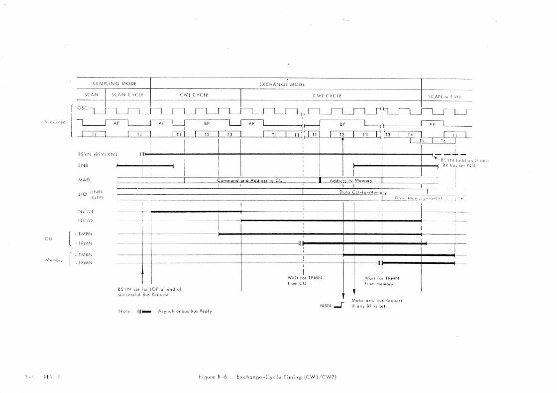
B.17 Exchange Mode
The Exchange Mode is used by the lOP logic to perform a data transfer between
a CU and memory. The exchange can be either input (eU to memory) or output
(memory to eLI). The lOP operates as System Master to obtain control of the GP
Bus and control the operation. The operation is performed in two logic sequensor
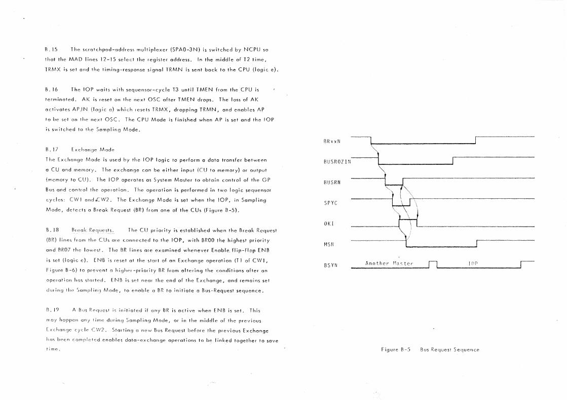
cycles: eWI and.eW2. The Exchang~ Mode is set when the lOP, in Sampling
Mode, detects 0 Break Request (BR) from one of the CUs (Figure B-5).
B. 18 fl,eak l(ecl'Jests.~ The elJ pi iority is established when the Break Request
(BR) lines from the CUs arc connected to the lOP, with BROO the highest priority
and BR07 the lowest. The BR lines are examined whenever Enable. flip-flop ENB
is set (logic e). ENB is reset at the start of an Exchange operation (T I of CWI,
Figure 8-6) to prevent a high"r-priority 8R from altering the conditions after an
operation has started. ENB is set ncor the end of the Exchange, and remains set
du. ing the ')ompl in') Mode, to enable 0 BR to initiote a Bus-Request sequence.
fl.19 A Bus RrCjlJcst i, initiated if any BR is active when ENB is set. This
moy hoppen ony lime durinq :';ompling Mode, or in the middle of the previous
[xchon')c cyel,. CW7. Starting a new Bus Request before the previous Exchange
hos been cornr"''',d enables doto-exchange operations to be linked together to save
I i me. Figure B-5 flus Request Sequence
St.:qu...:r1S0J
CU
1:f\.1
BSYN (BSYLXN)
ENB
MAD
BIO (lNR) ,ann
NC';: I
- TMPN
. TPMN
l( .- T MRi',
.. TRMN
BP
-] IUJ I T2 I . T3 I I T I
I I I ! ,
I ! I II
! I
I I :
I
Command and Address to CU
I~:~ I T2 I T3 I , , , , ,
I I I I , , I
731 -lt L 1-'-"-- -I -.IL_
I I I
I
I , I I
.-~-~-
I -- ...... -"-'--[3(,Yt'Jflt;ld on if ne'l,
-oij iH: hus 'C'I M'il.
I Addrf;U to Memory ~ ____ ~ ________________ ~ __________ ~I __ ~I ______ ~ __________ ~f-.----
-_===--_.~-__ -_-_.~=~-__ -___ -__ -_-__________________ -_-_-_-_--=------l--------"Dc:o:.:.:1 0 C U- t 0 - Me m,: y _-7"[)-,,-u-c, '-:-/,:-.. ,-, "-'-.;I.-Y-'----' ,-) _(' I J ___ 1
, ---------
I ---------i---Joo----------_---+---------------;-------------! I
1 -- ------- j----t---------- ------------------t---------IIIII----~+_-....... -----*-·----·-'Ir-
BS'(N set fo, lOP 01 end of sUl-cesslul Bu') Request
Note: III~ A,ynch,onous Bu, Reply
FiglJleB··6
----------------- Wait for TPMN 1-- ~---~a,::, TRMN
from CU from mernolY
Make new Bus Rcque~t MSN...r if any BR is set,
ExchClnge-Cycle Timing (CW j/CW2)
B.20 With ENB set, any active BR signal is set into the FBR register (logic e)
by the leading edge of !,P, which occurs every 200ns during Sampling Mode, or
at the end of Exchange cycle eW2. The priority encoder circuit (74148) indicates
the code of the highest-priority BR stored in FBR. This code (BRENCO-2) is used
to select the external-register (scratchpod) address.
B.21 Bus Request Logi c.
Moster, is shown in Figure B-S.
The Bus Control sequence, with the lOP as
BUSROZ IN from the detected BR is gated into
the Bus-Request logic (logic e) as BUSRO if no other operation is active (BUSRON
high). BlJSRO sends BUSRN to request the GP Bus.
B.22 The active-law SPYC response (scan priority chain) sets the OKA flip-
flop. OKI is received if no higher-priority unit takes control of the Bus. OKI sets
the MSL (master selected local) flip-flop, while OKAN blocks the sending of
OKO to the n"xt unit on the Bus. MSL sends the Master-Selected signal MSN
onto the Bus, and terminates BUSRN. The CPU responds to the end of BUSRN
by dropping SPYC bnd Of~ I.
B.23 The lOP may have to Vlait, with MSL set, until the Bus becomes free of
ony current opel at ion (TI':Mr'~, 1 PMN, ond BSYN all inactive). When the Bus
is free, MSL sets flSYlX which puts BSYN onto the Bus to toke Bus control for the
lOP. Thf' lOP ,,,,itch,,, to the CWI cycle at the first AP after BSYLX is set.
B.2-1 Regisl('r Addressin9 .. T v,o cnntrol-word registers must be accessed in
tlrr sClotchpod durinq tl", I::xchonge Mode. The registers contain dato transfer
information (conlrnl one! address) and must be updated during the operotion. The
·,Cfotchpad-oddlC>' multiplexer (Ioqic b) is switched by NCPU so that the BR
pr iorily "ncoder ond ~·JCW I select the register address. The three most-significont
bits (SPIII-3) ore selected by flfn:t'-IC2-0N; the least-significont bit (SPAO) is
.,,,Ir·ct.,d by ~'JC\'/J (J for cycle (WI ond 0 for cycle CW2).
Il.25 rirsl Conlrol Word. The fir,t control-word sequence (rigure B-6)
brqins wilh tl", first AP pulse followinn ti,e setting of BSYLX. The sequellsor
CWI cycle is AP-TI-BP-T2-T3, with AP of the CWL cycl0 following directly
after T3. The NCWI flip-flop (logic d) is set by the lcadinq edr)e of liP after
BSYLX is set.
B.26 With NCWI set, the ALU mode selected is A minus I (for bits 04-15
only). The first control word is gated from the scratchpad into the buffer register
(BUF, logic c) by the leading edge of BP. The Bur contents are immediately
applied to the ALU where the block-length is d('cremented and bits 00-03 are
transferred directly. If the block length is decrement"d to One by this operation,
ENDN is active. At the end of Br, the updated contr,,1 word is gated bock inlo
the scratchpad.
B.27 The Input/Output control bit (ALUOlt'-l) and the ENDN signal are sel
into a two-bit register (logic b) as BUf-It'-J and BUFEOR. These two bils are written
into the auxiliary scratchpod as SPINN and SPEORN, and are used to minimize
delay in the generation of the MAD signals to the CU.
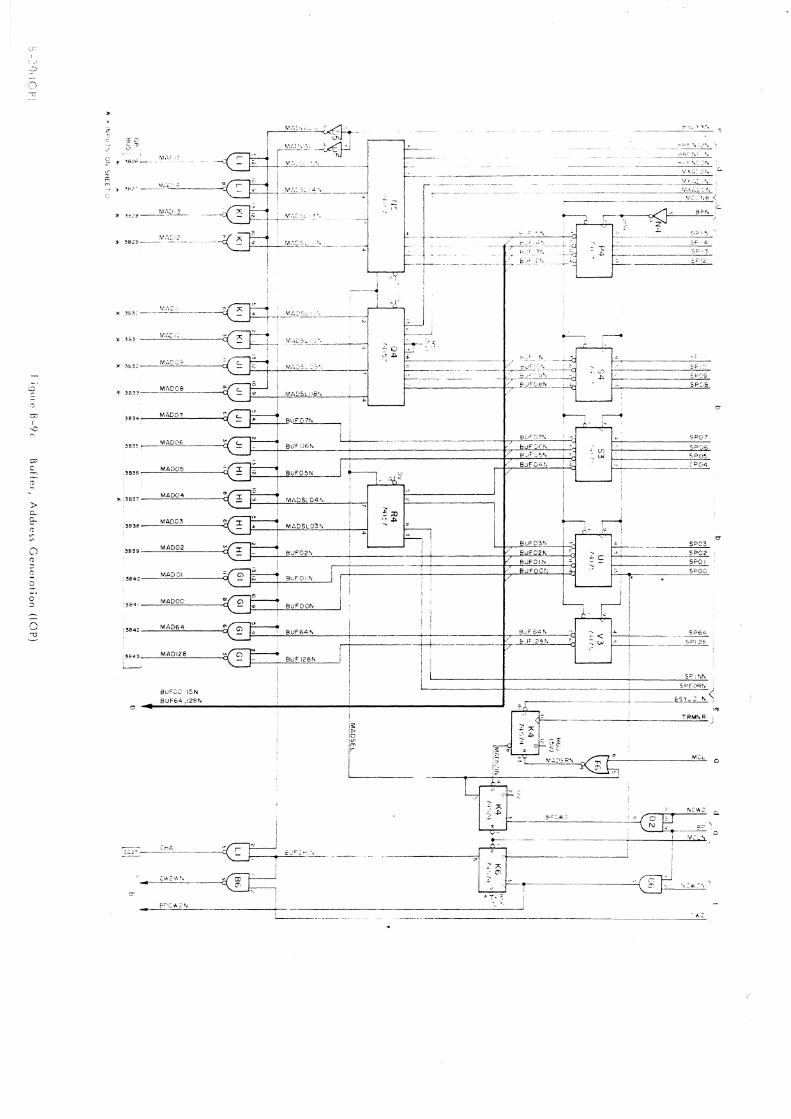
B.28 The lOP command 10 tI", Cli is placed on the: MAD lines (figure B-7)
via the MAD5L multiplexer (logic c). The Input Output conlrol (SPIN) and
EOR (SPEOR) bits are sent on MAD04 and 03 respectively. The 101' address
(MXADO-2) placed on MAD10-12 is taken directly from the 101' oddress l/-links.
The CU address from the priorily ('ncoder (BRENCO-2) is sent on MADI3-15.
B.29 The lOP generates Bus timin" signol TMPN (logic.,) at the end of time
T2 (the first OSC after flip-flop TMPX is sct). TMpr'~ 'lacs octive 160ns afler the
MAD lines are set. The CU uses TMPN to validole the oddre» and contlol
information on the MAD lines. The eWI cycle for the first control vJord rs
completed at the end of T3, before the CU has responded to T MPt--J.
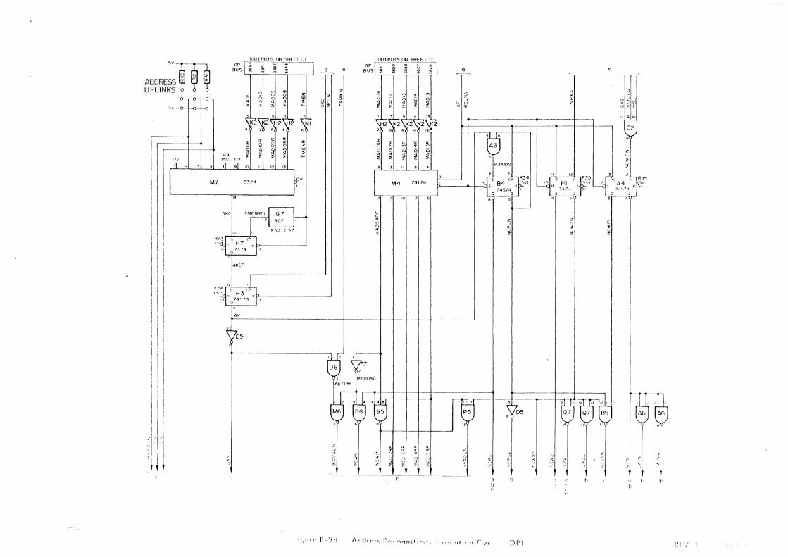
B.30 Second Control Word. 1hf' '.;"\ ond cOfllrol-word sequence (f'i~lure B-61
begins with the AP puis£' immediately followin,] T3 of eWI. The sequens", CV/2
cycle is AP-TI' -BP-T2-T3' -T4-15-T6, with 0 waitinCJ loop before BP ond lor-fore
T4. Flip-flop NCW2 (Io"ic d) is conditioned by th" TMPN sigllol (lMf'XA) and
set on the leadin" edge of AP.
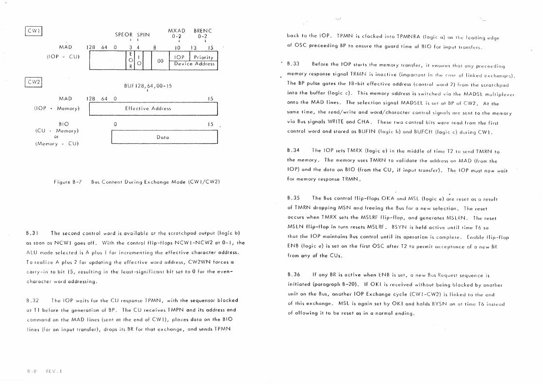
I cvnl
(lOP
(CU
MAD
(lOP· CU)
MAD
. Memory)
BIO Memory)
or
(Memory . CU)
Figure B-7
SPEOR SPIN MXi\D
0-2 BRENC
0-2
128 64 0 3 4 8 10 13 15 E
I I lOP I Priority 0 00 R
0 I Device Address
B U F I 28, 64 , 00 - 15 I
128 64 0 15
I Effective Address
0 15
Doto
Bus Content During Exchange Mode (CW I/CW2)
B .31 The second control word is available at the scrotchpad output (logic b)
as soon as NCWI goes off. With the control flip-flops NCWI-NCW2 at 0-1, the
ALU mode selected is A plus I for incrementing the effective character address.
To realize A plus 2 for updating the effective word address, CW2WN forces a
cally-in to bit 15, resulting in the least-significant bit set to 0 for the even
character word addressing.
B .32 The lOP waits for the CU response TPMN, with the sequensor blocked
at Tl before the generation of BP. The CU receives TMPN and its address and
command on the MAD lines (sent at the end of CWI), places data on the BIO
lines (for on input transfer), drops its BR for that exchange, and sends TPMN
back to the lOP. TPMN IS clocked into TPMNRA (logic 0) on the leoding edge
of OSC preceeding BP to ensure the guord time of BIO for input tronslers.
B.33 Before the lOP storts the memory transfer, it ensules thot ony prece(:dinq
memory response signal TRMN is inactive (important in the ,ml' of linked exchanq",).
The BP pulse gates the 18-bit effective address (control WOld 2) from the scratchpad
into the buffer (logic c). This memory address is switched via the MADSl multiple""
onto the MAD lines. The selection signal MADSEl is set at BP of CW2. At the
same time, the read/write and word/choracter control signals are sent to the memory
via Bus signals WRITE and CHA. These two control bits were n.·ad from the first
control word and stared as BUFIN (logic b) and BUFCH (logic c) dUI ing CW J.
B.34 The lOP sets TMRX (logic e) in the middle of time T2 to send TMRN to
the memory. The memory uses TMRN ta validate the oddless on MAD (from the
lOP) and the data on BIO (from the CU, if input transfer). The 101' must now wait
far memory response T RMN .
B.35 The Bus control flip-flops OKA and MSL (logic e) are reset as a result
of TMRN dropping MSN and freeing the Bus for a new selection. The reset
occurs when TMRX sets the MSLRF flip-flop, and generates MSLRN. The reset
MSLN flip-flop in turn resets MSLRF. BSYN is held active until time T6 so
that the lOP maintains Bus control until its operation i~ complete. Enable flip-flop
ENB (logic e) is set on the first OSC after T2 to permit acceptance of a new BR
from any of the CUs.
B.36 If any BR is active when ENB is set, a new Bus Request sequence is
initiated (paragraph B-20). If OKI is received without being blocked by anothel
unit on the Bus, another lOP Exchange cycle (CW1-CW2) is linked to the end
of this exchange. MSL is again set by OKI and holds BYSN on at time T6 inste(Jd
of allowing it to be reset as in a normal ending.

13.37 The ]OP waits for the memory response TRMN, with the sequensor blocked
at T3 before the generation of T4. The TMPN signal to the CU remains active
during the memory-transfer operation to enable the BIO-line dota at the CU while
T MRN enables 1310 at the memory.
[\.38 Th.] 1 RMN response from memory is set into flip-flop TRMNRA (logic a)
0n ony leoding or troiling edge of OSC. Time T4 is then set on the next leoding
cri,)" of OSC 10 continue Ihe CW2 cycle. At time T4, flip-flops TMPX and TMPENB
(109ic c) (He ".,,,,1 and TMPN to the CU drops (providing suitoble guard time for
Ihe CU to r"ad dolo on the [\10 lines). The CU drops TPMN after TMPN goes
inactive.
13.39 For rcael op"rations (output, memory to CU): the memory validates the
dnto on Ihe BIO lines vlith TRMN, the lOP validates the 1310 data at the CU wilh
ti,e troiling edge 01 TMPI'-1. For vllite operotions (input, CU to memory): the CU
validales the 510-line dota willr TPMN, the lOP validates the 1310 data ot the
nwrnc"y ·"il1, Ih" 1(~odin9 edge of 1 MflN.
B.-10
A block dio»I("" of 11,,, 10f' is given in Figure B-1. The control words ore loaded
intn the Control Word Regislers (scr'Jlchpod), via tire ALU, by WEfI instructions.
rhe CPU If'(HI<. a Control Word Irorn Ihe scratchpad by menns of an'flER instruction.
Durinq dnlo-I!'Jl1sf"r oprrotions (Exchonge Mode), the Control Words are accessed
and updolcd '.fio II,e processing loop: scrnlchpad--buffer·-ALU--scratchpad. The
oddrpSS-'lcn,,'oli(Hl lor]ic sends 11", CU oddless/commond and then the memory address
i01 cncll dolCl frnnsfer.
T I,,· 5eqU('(1S(>1 (Io'lie 0) is driven from () constantly-running oscillotor 10 provide
II", lOP liminq "i()l1ols AT', [JP, T I, T2, 13, T4, T5, T6. The oscillator frequency
(II OlJAfn I ie, )0 Mil:'. (Jnd OSC is 10 MHz. Sequensor cycles for the different
()pf-'ll'JfillfJ M0d,-,,> nle:
Operating Seq.
Mod" Cycle -_ ... _-------_ .... _---Sampling Scan A P-T], repeated until CPU or Exchange Mode is se t •
CPU CPU A P - T ] -13 P - T 2 - T 3 * , woiting at T3 unt i I the fi rs t OSC
after TMEN i" received from CPU.
Exchange CW] AP-l1-BP-T2-T3, followed by the CW2 eyc Ie.
Exchange CW2 AP-T 1·-BP-T2-13 '-T4-T5-T6, with 'NoitinfJ loop be fore f}PondT4. AP of next cyc Ie (SconcCW])
follows T4, overlapping T5-T6. ----------.
Signals AP, Tl-T4, T6 ore clocked on Ihe risi"" edr)e of OSC. Si!lnols fir) and
T5 are clocked on the falling edge of OSC and thus shifled one-llOlf OSC e\"e l ('
from the other sequensor signols. All sequensor timing signols hove 0 durnlion
of ooe or more lOOns OSC cycles, as follows:
• • •
B.42
•
AP, 12, T4, T5, T6 ore olways lOOns.
SP is lOOns (CPU cycle) or 200ns ((W I 1(1.'/2 cycles).
TI or 13 moy losl for one or IT'ore multiples of lOOns dUlin'l the Mli!in'l
conditions for [H' or T·1 d!!rinq the (\'-/2 eyel('.
The conditions fOI th(; Scqclpnsor timing siCJnoh ore:
AP (first pulse of every cycl,,)
Condition
Scan T I Sterrt of Scn.n or CIN I cycle, dependin') lOn condilions fm ill'.
CPU T3.AK"J Starl of Scnn cycle; S"quensor "oil', 01 T3 01 (~PIJ eyel" until
CWI T3
CW2 T4
A K hJ in die (] I C' 5 the end 0 f t h (~ CPU (" 0 nl IlHHHi, t 0 (l '/ 0 i d tJl (J n c h ; n (J
bock into 0 CPU eyel" if TMFhl is d"loycd.
Start of cvn cycle olwoys follows 13 of CWI.
Stmt of Scan or new eVil cycle r"lIoNsI4, alll1(1)9 h i5_[i. "f
CW2 are nol complele. L-______________ L ______________________________ . ___ ..•. ___ ... _. ________ . ______ ._ .• ____ .•.. __ __
• T 1 ~-----------.-----.-- -.----.---. . _ .... _-_ ... _ .. _--_._ .. _------_._._ ... _---_ .. __ .,
AP
BP T] follows Iii' for 011 cycles
W (J it (J I T I un til B I' i, se I (C VI? c y el c)
• BP
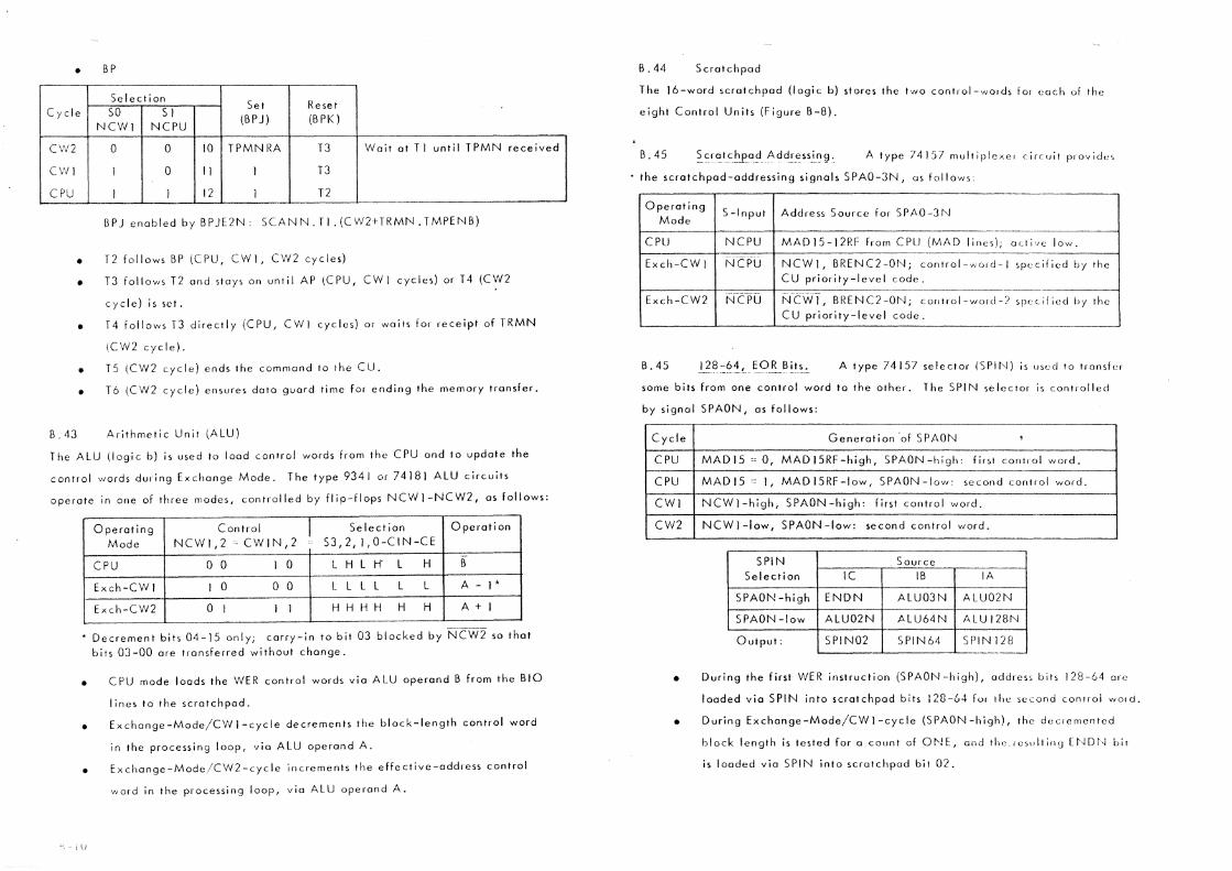
Se I e ct i on Set Reset
Cycle SO S I (BP J) (BPK)
C'vV2
CWI
CPU
NCWI NCPU
0 0 10 TPMNRA T3 Wait at TI until TPMN received
I 0 II I T3
I I 12 I 12
BPJ enabled by BPJE2N: SCANN.TI.(CW2 I TRMN.TMPEI'IB)
• T2 follows BP (CPU, CWI, CW2 cycles)
• T3 follows T2 and stays on until AP (CPU, CWI cycles) or T4 (CW2
eye Ie) is se t .
•
• •
T4 follows T3 directly (CPU, CWI cycles) or waits for receipt of TRMN
ICW2 cycle).
T5 (CW2 cycle) ends the command to the CU.
T6 (CW2 cycle) ensures data guard time for ending the memory transfer.
B.43 Arithmetic Unit (ALU)
The ALU (logic b) is used to load control words from the CPU and to update the
control words during Exchonge Mode. The type 9341 or 74181 ALU circuits
operate in one of three modes, controlled by flip-flops NCWI-NCW2, as follows:
Operating Control I Selection Operation
Mode NCWI,2 CWIN,2 S3,2,1,0-CIN-CE
CPU o 0 I 0 L H L H- L H B
Exch-CWI I 0 0 0 L L L L L L A - I *
Exch-CW2 0 I I I H H H H H H A + I
• Decrement bits 04-15 only; carry-in to bit 03 blocked by HeW2 so that
bits 03-00 are tronsferred without change.
•
•
•
1\1
CPU mode loads the WER control words via ALU operand B from the BIO
lines to the scrotchpad.
Exchange-Mode/CW I-cycle decrements the block-length control ward
in the processing loop, via ALU operand A.
Exchange-Mode/CW2-cycle increments the effective-address control
word in the processing loop, via ALU operand A.
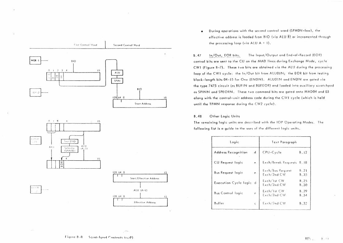
B.44 Scratchpad
The 16-word scratchpad (logic b) stores the two control-wo,ds fOI each of the
eight Control Units (Figure B-8).
B.45 A type 74157 multiplexer circuit plovide'
the scratchpad-addressing signals SPAO-3N, as follows:
--Operating
S-Input Address Source for SPAO-3N Mode
CPU NCPU MADI5-12RF from CPU (MAD lines); ael iv e low.
Exch-CW I NCrU NCWI, BRENC2-0t'>l; controi-vvold-i ,pc c ified by the CU priority-level code.
----_._.-Exch-CW2 NCPU Nev(f, BRENC2-0N; control-word-? 51)(' c ifi"d by the
CU priority-level code. ------
B.45 A type 74157 selector (SPlf'l) is used to tlonsfcr
some bits from one control word to the other. The SPIN seleetO! is controlled
by signal SPAON, as follows:
Cycle
CPU
CPU
CWI
CW2
•
•
Generation 'of SPAOi'j ,
MADI5 oc 0, MADI5RF-high, SPAON-high: fir st control word.
MADI5 I, MADI5RF-low, SPAON -low: second control word.
NCWI-high, SPAON -high: first control word_
NCW I-law, SPAON -low: second control word.
SPIN Source Selection IC IB lA--
SPAON-high ENDN ALU03N ALU02N
SPAON -low ALU02N ALU64N ALU128f'-l
Output: SPIN02 SPIN64 SPINI28 ----
During the first WER instruction (SPAON-high), add.es> bits 128-64 are
loaded via SPIN into scratchpad bits 128-64 fOl the second controi WOld.
During Exchange-Mode/CW I-cycle (SPAON -high), the decremented
block length is tested for a count of Ot'JE, Gnd the te>LJltinCj [~~D~--J bit
is loaded via SPIN into scratchpad bit 02.
8-
r~ ~
n ! '?
f il\t Con!lo1 \Vold
BIO
11
15
r iqlJre fl-8
Second Control Word
BIO
15
15
St(lrl/Ef!('ctivr Arldr(>~s
ALU (1\' I)
15
• During operations with the second control word (SPAON-Iow), the
effective address is loaded from BIO (via ALU Il) or incremented through
the processing loop (via ALU A + I).
B.47 The Input/Output and End-of-Record (EOR)
control bits are sent to the Cll an the MAD lines during Exchange Made, cycle
CWI (Figure B-7). These two bits are obtained via the ALU during the processing
loop of the CWI cycle: the In/Out bit from ALLJOIN; the EOR bit from testing
black-length bits 04-15 for One (ENDN). ALLJOI Nand fNDN are gated via
the type 7475 circuit (as BllFIN and BUFEOR) and loaded into auxiliary scratchpad
as SPINN and SPEORN. These two command bits are gated onto MAD04 and 03
along with the control-unit address code during the CWI cycle (which is held
until the TPMN response during the CW2 cycle).
B.48 Other Logic Units
The remaining logic units are described with the lOP Operating Modes. The
following list is a guide to the uses of the different logic units.
l.ogic lex t Paragraph
Addre ss Re cogn i t i on d CPU-Cycle B. 12
CU Request logic e Exch/Ilreak ReqlJ('sts ll. 18
Bus Request logic Exch/Bus Request Il.21
e Exch/2nd CW B.35
Execution Cycle I ogi c d Exch/isl CW B.25 beh/2nd CW B.30
Bus Control logic Exch/lst CW B.29
('
lxch/2nd CW B.34
Buffer c Ex"h/2nd CW B.32
, I
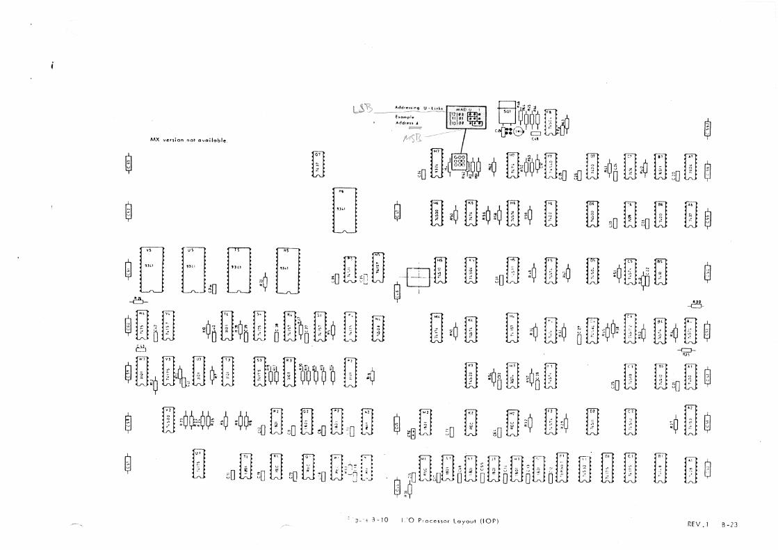
B.49 PHYSICAL
The Unit, are contained on printed-circuit curds (F igure B-1 0) of the standard
P852/856/857 system size. The parts lists are provided in Table B-1.
The lOP interfaces the other system elements (CPU, control units, and memory)
via the GP Bus, via connector-3.
B.50 U-Links
Adjustable U-links are provided for decoding the lOP address (logic d). The
locations of the U-links are shown on Figure B-IO.
B.51 Break-Request (BR) Signals
1 he Bf{ signal connections are shown in Figure B-ll. The internal BR signals,
from CUs in the some chassis with the lOP, are attached to connector-4B. The
external Bf< signals, from CUs in the extension chassis, are attached to connector
5, and are strapped from connecror-4A to 4-8. Priority of the contral units is
determined by the order of the connections to connector-4B.

I
1 d
t I
« z
" l'c
"
"-~--------t-~~~~-
"-------""--~-"--___t__t"-_.
1v'IrI..N
I 1-,"- '0 c
f~- " IMI ~-?MN
1 10
':J,"~,w, .
fRMt'!~_~_~ __
______ ~~2
.. ') U if) 'J1 o n
d
d
E ~ " ~ '" <1 z z
~ 0 Q ., C1
d.
~ :1 '"
" .,
b
6 r4D~~ ___ _
_____ __ -..J.l..sJ,;tL ____ ~ ___ ._ ..
~~~~---.~-.-.-
" m
b

l,-03
SPA
k~,1 ~~ 1-1"')2 _2~
- R48 2E'Er)HN
H49 s~
',.
14
I
d , .;t <1 i'J ? (\j ~ (\j) ..s ::- ~ ll. "" (' ~ ',J U,
2
-----, L~
." .: L.::' ~; <: p) ,\I -, "5 :-::. :::;
-
6 III '.'
I I',,:·; '\l ':>1..1 l~itS SHfET
~2~~ "") J J :J J _J _J ..J
<t <.1 "-l <t
Hluvf.{.2 I ()V -ll ''-,-;-r-cr--:-r-'
ll., ',-:-"- . ~ I ~ K2 K2 ------:'!'-:t--::'I~_;;f~r_;;]
" ,J, ,n c, c)
el " ~ "-if> '"
L::::. 1'\ i'.-
~l~I~J'~' 6 , ,
" M
~ ~ " 0 0 0 0 0 iii iii ID
~~ z " z
" " N ,-, (~? Q (il m
::; , ~ " " ~
INPUrs AL::'O r· '.)N fHIS SHEE f l~ "
figlJlc; B-9b
d
OV 52
SCRATCH-, 'il ., PAD I, '" U 0
5~ " ~ ~ e, ~) B, " 'f> if>
i'. [':,. L::::.
-r -'1: ~'I~I~'I~) II ff" NI NI NI
z z "' z ;i, ~ <: 6 '" '" ...
<) () 0 0 0 0, 0 0 " 0 () 0 0 iii iii m m iii iii .
" ~ ~ ~ ~ .,
~ ~ ~ ~ ~
/,LU, SCiolchpnd (MX)
~ Z o 0
~ 3 " q
0
" u
"'
'09) NI
z 0 0 0 iii
ru
ov
(41(O J ,_' S6
S5 UV
:L "' '" e) el
d
0
'" n
"' <) /
:;,/
/1 < u
" ;.
" ~
1"'1 PJ
/ .. I
1 1
, c,

~ , '" "'
'"II
..
, II
- ? 7. '(1
u.' \!
b
.1y)~ .... _-, I
I , I ;, I ;:i ii .~~
I,

5\/
~ ~ {. ,'J ,'., ,j
~; ::.: ~ ~ ;:;,
(ouTPuT~) C<'< SHfETCl
Lfj,-~:J---~=] (OUTPUTS ON SHE ETC)
GP BUS
0
" ()
" .,
'" '"
n:
" (2 0 0
" " ~ " If.!
'0
9,~?4
MeF
", '" (; 0 ~ D 0
" '" " ,. :> >-
~2 2 ,
" " <r en CD (' " Z 0 " "' ., " '" ~ ~ ,-Il "
,lV
~~I
a /""--",""
3 "' u 0 :>
---- --------_.-
-_._. __ .-- ---._--- -----
[-------_._--... _--
BGts ~ i ~ ~ ~ c----- ...
z x
'" "' r
" N "' "' 0 ~ 0 u i, il ()
<t '" <t ., :> ,.
" :> ,.
'" a: '" " " " 0 N '" ~ '" 0 " " 0 () <t ., '. ., ./ :> >: " " ;,
" 02 741/4
,0
-------~-··-----~9 ... 'O.,~~" ~
2
<1
a MA004A AKTRM
4UJ~~ 9 ",0 P6 L7 K7
6 ';;
Z J
<t > o <ii
4-
Z ~ ~J
~I ~ ~ ~t :?: ~
·-----b--
4- " ?; "' '" 0 0
" <l :> "
a
7 --
"; 0
~
., , j
<L r ' ? (/1 if. Will ::>'
~------------~----~--,
---.>-----1-----.--+---1- - C4
iV'F7' ) C!-'1J()N
to! II
IJ~ (J £6 C fI 5V
1 " 74574Q
C> t> u z
a b e
"
z ~)
t> u Z
N :J
f', z
b
G5
Z OJ
~ z
)r'
-1.1, Ii C5 D.s ":;V '-..-.:' (:£6 (j ')1/
7q 1'4 '4'.~ 14 w ~ (J 'J Q IJ
, b
Z OJ ;; or ~ N
" ~ ~ ~ .:.t z "' z u
a 1I tJ a 0 b b b b c c e
Figure B-9d Address Recognition, Execution Cycle (MX)
.,
" I>

r I'if CI,tmF(,Tnr1'l 4 "NO 5 -TSEE··TfTIT
" " " '" • -~-
~J ;, ~ z :i, 0-
r. '-, '> 0 0 0 0
~ :}, ;~ <r 0-~ :li m m
0 d ~~
IL ;:: i OJ OJ
" '< , ~ u v z .. q
-~---~--------~
u
'" 0
z z ->w U I:!'
H--i-l!--------t----~-__li__'_--
CU REOUEST
d (lU rpUT ANn INPUT 'IN nils <,Hff T
~-+-+-----t_-----_t
BUS~~Q"'Z"""_N ___ ,
BUS REOUEST
[~ d
Z
~ m
m ..
SPYCR
..J Z 0 5V
'" '" '" :> " 0
d [~---~ 1
a a d a
:'i z N Z ~ <t ~ ~ t'. I- ~ U
0 z :> Q ,
~I .,
-+--\---j----- ~-~-
------~·-T- -t-~t-i_t------ --- i
"
I ----1---1' H2 12
z N cc Ir
Z' ~ -, " >-
'" e: n: In ,~ .
n a c
·,1
"
F7
87
BUS CONTROL
., X a. ~ , ~
lMPXfI
HI
-' u >
[;~ I
I I
., co ,-'" 0
.:
I
'-v-C7 I
I
/ rr )'
r~ .,
x )' 0-,
HI
,. x
~J "
pr \; ..
,j

lJj
MI
I
I I ,I
I J~ .' '~'t " u,~ J t ~:t ~
~ I c:' lOP) tel'''!
J
'" ~. $ .
" " a.
:'1
I
I
.
I
t
I '11O!L
T
i· t.'~'h:t.1~
~ L ...
Figure B-9a
T'3RN
" " 3 "- .:: « , D
• T4[)N
T4N
__ -..Q:CN_~_-+ __ +-__ ' __ -1. _______ _ MCU~
z n w
a. m
b
C lock/Sequensor (lOP)
I
t
d d
Iril',jT',
," :>11',
;, <
(,, ." <~I If f ,
ro
HllFOO J5N.!{} f~UFf,4,!2BN§
ro
--
P2 P2 P2
; ... ., I,
i,
n [" ll'l'lt' "'''' S A\ 50 :; :!; ~ ON THIS 5HFfl [;;lm ~j ~J ~-l [~J~~S 'j ~
z ~ z z ~ ~ "' N )
0 0 .3 6 0 {)
" <' iij m <ii 51 m til
0 ~~ <0 'J ()
:}l n ~, :}, f},
" " " ''.,
_~~,_~_, _____ ~_,, ___ ~L __ ' __ __
--I to q 13
P2 02 02
~I ;;. ;;. ? ;::)
e, (-) 0 0 IJ
c~ 0 " u m iil iD
~ ~ ," ::
, i '1"'" f\ _C)f,
'-I ~J 0
0
~l ~ rnl ~JGP ~~ -~ §~ ~ d ~ ~ BUS d
8 N Z Z
~ 3 ~ Q 8 6 0 v ;t ()
" en co 0"1 iii z m m (i ~
,J
SCRATCH- ") 'e " PAD ~ N
"I ::: " ,n
~ 0 'e I,
" ,) e, ~,J n ~}l V' V\
, , :~l "
TI TI TI TI
"", 7f, ;; " " ') ., ,', 0 " .n m
~ " :: ~
z 7
81 -
~ N Z :,
", n 0 'J,
" ")
~I ~I :~'~ m n if'
I ~ ~ ",
() .''0
LS
co I
--0 r.
"" C
(')
}> CL CL (') o
Cl (1)
" " ;:,
o :0
o -C
2- rS"-'".~~ ~~ ('{ ~ ~~~ ~.
m ~-"::'----:'--~ JI ~-------.j ~ y .---------"'~ : --. -~+-, y-,- - ':'-
>' ,cce-Y'L@.. . ... ! 2 f I
::r.;-, c'U Ir
~ "" "'6;>f:~·-~. ~;\' "
" ~
~, r-. \ .• ..,:.: ;C",
-~-- - :,~,:,~~~ ,'~ . ----, _ ~~_ '.'"'~ . r.·~ <
. ",.. "j ,".' ". .. I "I I
> '.29_",=,2 __ ::.f ~ : .. U.i .... 1 ~C~C ...... ~-··t--------. .:. I: "-y' ---r
-'--. , .. ~., : o~r:-~---:~'~ ~;~::~ J~ E ~~- ",: r- -- ",,:
I .. ~
---~')' i
I- , __ . • - ~--...':.-.:.'~---- ~ -
",' ,'- 0", " .. , l 'c ~~ ___ nL; \_ ,., -:~~.-, :": .••. ~. .. --'=·Y·;',;( ,'"" ~
6 I • ~ '- <fl I MM~.bl..!?-~ .to
3."-""" - I ",,, I ~I -BuFc,n I, i .-------=--ti ~~,~~~~. ' ""--- ..• ~-' n ~- , ;;"", ,
~ 1/,
383t-· '"'' ~ L.. :: :r: ~ BUFOSN ~AD05 _
3." I
~. 3537 MAD04
l~ i ~~3B
I
'"
.............
~ ~ <;:P'~'9
SP:::-:6
SOC?
pc.
SP05 : PC,4
MADC3 ~ M~DSL03'
3B!9 MAD02 ~ B:~d~_' --. BUFOIf\;
__ 5P03
~ BUF CC - i I
3840 ~ MADel ~ 9LFOI ~ I I ~ _
_ -"'M"'A"'D"'OO"'-___ ~~ ~~ BU'CO' =()L' '.- Ie f IU, ~ ,
i I
{.O.; _ . __ .;2~~6.~... ._ ~: < :.. , . ___ _ ~ M:"D64 ~ BUF64"" ~I ______ .~_~__i__ __ .___ >T ;.. .. j~:2St, (" :: OJ ."" '. _._ 394< '-=.Y-- r-j--___ .. ~_______ __ 7'~-;;'-~- ,. !
N I i 3843 MADI28 G==: BU'i28N
auF")':' --lS"", ~
BUF64) 1281\; cr
_~02
SPOI
SPOJ
___ 5 P6 4
SDI2::-
s::> , ~~I\ SDE·.)Q!\: :
ES,(~:~~
TRM~q
C'
0'
:~ • ;: ~2 .iP: V':':;5-R:,\ ~ W':L
_~'7~.".. '" .. 0
'-' -..;
"A 2'" " , v-
~- _ .... ~'" o' "we,"-tv .: __ 3::- ~
~o ...-. 1J=-:-" - ~. . -:' ~ ___ ._.--1 ~A
~ cr.," ._-----.---- f'0J ':"'r.~' ~'
-~ ~~-. -.c.'""'---~-r =CC?".:c __
-_--':W?'.:-.-----~
~~C'IoZI\i
L ___ . __
rN ~)'J (')\/) 0'1
i'l.I<C
a: 6 <l :-
93?4
<:' o <, "
'" Q a ~
"
U> <Xl o 0 o 0 <t <! ~ ~
" :Ji '" 0 0 a 0 <l ., :> "
"
0: z uf
" ,-
Z <) • .J
'" U o~
-----------
7 , ·f
"
GP BUS
(OUTPUTS ON SHEET C) ------ --------.::---;;;--] ~ i ~ ~ ~
cr ·t o o <!
"
"Q
" o a <!
"
N
o -, ~
aN () <l
" " M4
:li is <f
"
"
74114
a ,r--- ..........
<f x Q
E:
- ----- --- -- -----------1- -------, .
z " Q. e) Z
I
---- ---j---j--_J
u- I, ., ;;, " .- "' < ~ u " C' -, .. " ~ ;> ;-
···---··Fl--
u. u ~ !Y
:~ " ., ~ ;~
P5
<, n
1\ d d! r' u, P (' t ("1'1 n i fir) 11. r)o', f' I 'I f ; ("' n (' v (
o b
<, n
D5
:)P)
h
II <;I 10
C2
I
i
I
r~~I(: I I
j I I
,1;( ;j
[~I- 1/

101Q~ """ . I . I I : I '1 I I I •
I I I I I
f It! J ··fi~ I I t---I I
I I I
81
"' 'j ., z z Ii' ~
'" m <L
3
" '" v v Z Z w w
ffi oc '"
.<
r--.9---v- b
. ~I.':' ~ '-1 ~t u 0
2. 7.
I
CU REQUEST
d
}\ (juT PU rAND !NPuT <ill 1 HIS SHlET
o -----"''",
-, v II
OI<IR
a
z " " Z ~ a. , ..
d
z , ~ v " V> " 0 L
-------- --- ----- ------f-----f---.------j----_+__. ""------ -- -------------1-----
I l_tJ"~;" ).t1N
BUS REQUEST
'" ~ )-
"' en
*
Input/Output Control (lOP)
" " z z ~ ~ (l " l- I-
a a c
1--+-------- ---- -1-+ _______ _
BUS CONTROL
., x (l
~
z Q.
~ l-
~
C3
<l
"-'" ~ N X
(l <r
~ ~
a b
__ u __ _ __ .\l:i.,...ti ____ _
,. , C3
fj x ,. :':
N2 N?
Z L rr ~
~ rr i-
~l "I
~I <,
z ~
" fr:
MX version not available $
~ Ii! 50 !;J( r~ ,0,0 ~ Gl'OQ~m~ rD ill ~O W ~ W cO ill 0
® EJ s ill ,0 !ti,o~m!o ~ liLo GLDW fih
~E1 Et[J~D ;0!ilo0 9QID ill '08 '0 W'o ill 'o0~EJ ® -8- Lfl -c~
® ~h ill 'On @~05 W d WQ5 w,o [J ru w '0 III ill '0 G}o ~ w'oo{j,o w ~ W ® ~J ~
$ W1 ~kJI ~ W Woo W~ooo Q Q ~ lil ~o G:I ,00 til '0 W W1J GJ ®
® [H~,oo, ,0 'o~ ell ~lo !lLo ~Lo Q ~ ,0 @ '0 Q ,0 l!H El ~ 0 0 '0 W 0
® III ,,0 (iLD Q '0 !!lo Q,:~] ® ;~oGlowdGJ~@o0dIiJDill ill w ill 0 ill8 : ~,'; 3-10 1'0 P'ocessor Layout (lOP)
REV.18-23

Table S-Io Mu"ipl.'·~ COld Parl~ La!
52,53,55
s:;.
• G1, G2,~I, .·,2, L! ,MI, NI
0" "', -" ;4, ;" D"E5,E;,f5, Go,
'3.
'4
:;:'~1~,20-23,51.52.
, I - , ,4, 31 -39, 4 . -50, 5] -56.
:3
I 0, 28, ? 9 , 30,42, 61 , 62 .
IS,2S,2~,,},4J ,59,~O.
B-24
Desuiption
PriMed c !fevi,
Integroted circuit 3101 A
Integrated c ,rcvi, 7400
Integrated c irCvd 7402
Integrated ci"v'! 7404
Integ, ated 7408
Integrated c ir, viI 74\ 0
Integrated "Icvil 74r
IMegroled circvil 7474
Integrated c !reuit 7475
Integroted c ire vii 74 J 48
Integroted ,ircuil 74153
In1egrolt'd c i(cu,t ~ I 57
InTegrOleo - 4174
Inlegloled c ;rcv" 741 -j
'n1eg:o'ed eircJ;' 9324
Ir,'e 2' ated ;'4181
In1eJ'Q'ed ei'evl! 1801
1r"I,eiYQ'ed ci:.;:uj! REC O~13
,nlegIQ1t>d "4lno
If)ll:':gloleo ; 4HS)
In'eg1oted clfe .... i! 74$00
IntegfQted eire u;r 74S04
Infegrcted cirCuit 745 I 0
Inte:groted circui. 74SI1
Int~9'Qled ,ircvit 74S20
JrlIl:':groted C ffev;t 74540
Integrated c ircui' 74574
J,"egroted , ircvit 74$ 1 J 2
T ernet
Reli$lor 215n, 1/8W,
Re,i,tar J J 6n, 1 'aVi ,
p e ~i 11 01 2.15Kn, I/aW,
Rej,i"or 3. I 6Kn, I/aw,
Resi\IOr 3300., 1/4W,
Rui$IOf 470n., 1/4W,
Resistor 51 On, 1/4W,
Resi$tor 560n, 1/4W,
Re,islor I Kn, 1/4W,
Re,i~1 or 3.3 Kn, 1/4W,
Re1islof 5.6Kn, 1;',4'11,
Rei;S' :::;,r 100", I 18'11,
I 2NC Code
5111 10005473
.ito;,.
~ I "0_
:l.1",e..
:2:1%.
±5%.
1.5%.
:2:5%.
.±5'%.
is'',,
i5";..:.,
,5'0.
II ~c.
Reference
C48,
0,11,19,20,22,23,25,27-29,31,34,35, 37,39,40,43,45-49,51 -56,56,61 -66, 68-7I,74-BO,
(10,36,67.
(1,3-0. 1>18,21,24,26,30,32,33,41,42, 50,5/,.)9,60,72,73,81.
(82,
LI, l2,
10,
TObleS-le contd.
Oegriplion I 2f'~ ( (odt·
Capacitor 66pF, 63V, 2°", ceramic.
Capadtor 1 OnF, ceromic.
Capacitor 68_F, 16V, crS13.
Capacitor 3 ,3_F, 16V. (TS13,
Capacitor 560pf, 10%,
Indue lonce.
U lin~ DCW06.

1'),B'>,D7
" Al.
A I, C6.
RS.
A6,07.
C7,f4,H7,K6.
W'.
BI.
AI.
P.eference
H4, N5,0.4,R.t, V.4.
M ••
C 1 ,D I. N. 53. SA.U I, V3,
P6.P:5,T.5.V5,VS.
P3, R3. 13, i 4. U3, .. 'I).
Tobl~ B-Ib lOP Porh I.i'l
Ducription
Prinl~d circuit
Integroted circuit 7400
Integroted circuit 740i
'ntegrated circuit 7404
Inlegrated circuit 7A08
Integrated circui' 7410
Inlegroled circuit 7437
Inlf!g.ated circuit 71,74
InregrGted circuil 71,75
Inlegrotl!!d circuit 74148
Integrated ci'cv;1 74'53
In1e'i!,ot.d circui' 74'57
'ntegroted circui' 74174
Integroted ci'cuir 74175
Integroted circuit 7A'81 (93.40
Integrated circuit 9314
Integroted circuit 3101 A
GI,HI.JI,KI,ll,Ml.N2,P],Q2,R2, Tl. 'nteg,ated circuil 1801
r'2,K2,Ml,NI.PI,al,RI. Integroted circuit RfC 0613
D6,M6,'12.
DS,F8,KS,N4
O,J,C2,C3,M5.
B7,D2,H5,PS.
KJ
[I.
F7.
D •.
A4,6 4 ,C5J2,FJ,fS,H3. HO,K".
C'
"J ?~4
• .14 .
"S p46.
"'Sl.
~JO
oJI
"6~? , JI-1O.72-15,n,2B
IIl,A, 5,10 'l I , 26,19 ,J'l ~ 4'l
C.50 63 .562
C61 c·.
47-51. 53 -63
C"
C819,JI-AJ.'.l4,65,6B.,-O-;)
" '"
In
Integroted circui' 74S00
InlPg.oll'!d circuit H50..4
Intl'!groted circuil 74SIO
'"Iegroted circuil 74$ II
In1eqrated circui' 74S20
fn'egrr:)lfod circvil 7.4S30
Integloled circuit 704S40
In1egro",d circui' 74$64
Integrated circuit 74S7,(
Inl,agraled circuit 74S112
Ru,"or .6.tn,
11:.,;,,01' 681n,
Relil'or t .47Kn.
Re,;,tol '1.15Kn,
Reliltor 3.16K",
Re',lfor lOOn,
RI'!,;Hor 330n,
R~lj'lof .5 IOn,
Rop,;"o' 5~On,
Rop"Hor I Kn.
C']nocilor 47~ F ,
(oo.,cilol I O~j F ,
r:'Jpoc;tor 560pF,
(opoci',y .470pF,
Copoc:;,o' 3JpF.
C(lPO(;r'J 10.,F,
a ,0'" ii,'.''': 0A~OA - :!O~
'/ew, l/eW,
'/ew, Ilew, IISW,
1/8W.
1/4W,
1/.4W,
1/.tW.
J""W,
IOV,
'l5V,
12V,
1%.
Ir.If~ .
''''. '''. '''<. !"~ .
5',
5",;,
Y"-
5-'
eleelfO
f"1l'clIO
I";', O'T'Iic'opl'Jr ';0
(t'.,.,,,,ic
c~ro,..,jc
12N( Code
5111100 0605,
EXTENSiON CHASSIS
~XTENS!ON
CHASSIS
CU on lOP
I B. CU-' 3M3 ---------
SR (I) -3 3A42 III eR C:U-l 3A41 BREAKS
t=:;s:~~:g:~J:::;:==l 6 R C U -.4 3 A 23
In'oe.nol Sff'ok,
FigureB-II
EXTERNAL BREAKS
MAD
3A361
lOP g",.-Rt'que.' Logic, ol'ld AddreH;r>g
BROON-Q7N
I I
J
Break-Request Signal Connections (lOP) REV' 8-2'1

8·26
1801
3-101
J':'
7400
7400 SOO HOO 03' a 7' 38
1801'
:'> .. .i I.\~..,,,,v
~,.II A-,c>,
we i'''~ &. ,~"'~ cs :. .... pl;;; ••
0, 0 0 04
D D ,V '~" '~
IYiY,Y:Y ~ 56 710912tt
7402
7404
7408 7408
09 '
loprn
QUAD~UPlf :-lfJf'l'l
PO)17Iq-NO~ GATt
V U VO 'D -- 13
" :D·y
Ve< ,. GNO
7404. 504. H04 7406 7414 ", 7416 o.{. :
~ ~ ~ ~ '~ 1~
,:c !4 ,···.D ,
(0 \! rc tor o o '0 '0" 13
FigureB-12a
7410
7411
7410
~'1 '~
1~~ '~L/
PO~ I T I vi l"J~ j, .
• ·m s.zD-v
7411
p 0 S : ~"/£ l C ,:
~ " t..'
." 14 t.~o i
0, 12
"
D :D azDv
7420
7420 7440
6ufHP.
D 'D" • " 13
POSlTlv£ lOGICAp
Y,,~m r~ -y
0-3.11 "'.C H,14
lOP Ie Guide
7430
7437
7440
7430
ip " '2
( ... 7420)
wee 14 (.';1; 1
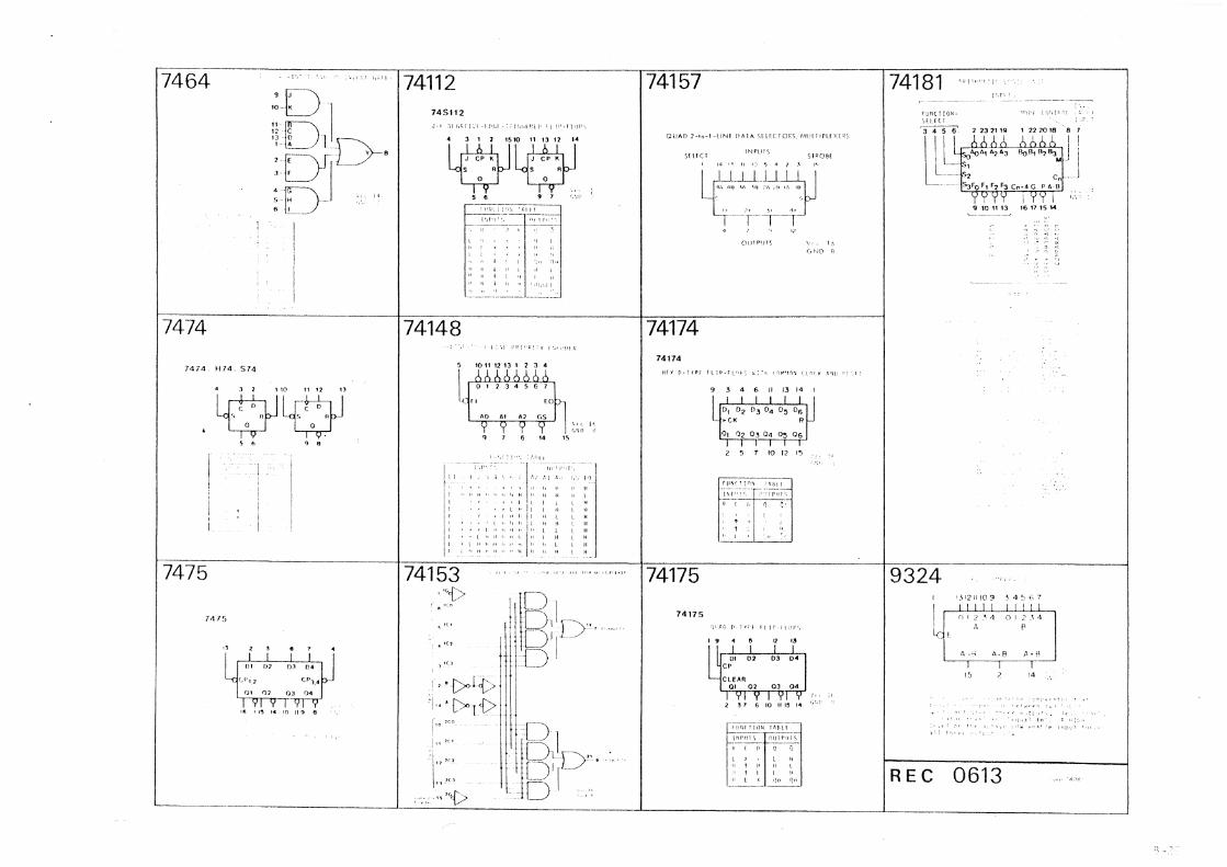
7464
7474
7474 H74. S74
:l 2 1 10 11'2 13
V:o Jlv·o " Jl ~ n o 0
.., 6 q fl
74112 745112
Lj! 1~7 \~~! 1~7{~'
74148
5 (; 9 7 ' > '.
\',1",'
I " " I II i h
',I
Z
" " 1
i: ~ \ I',
3 •
, . ;·"It
r,,' ,~ I t
" H I I
H
" I
' 1 ~ Ii
l ','f I 1,'111
"
1 I 1
l I
74157 74181
2 23 21 19 1 22 20 18 8 7
INPUT ~ Sf. Lf(T ')1P0!H
r-~~!~L-~~~~ I J
,., II " ,
i 9 10 11 13 16 17 15 '"
OIPrl)T(,
74174 74174
4 6 II 13 14 I
"
2 5 7 10 12 I,)
"
H
'~~--------------------------~-----------------------------~~-----------------------------+~---------------------------~ 7475 74153 74175 9324
7475
,,"{>
'" [>oC{> 'i"'[>r{>
i" ,., 1" 1~ 1
j'l?CJ
IC)
1111,8:111=>"" Ie)
74175
fllr
I 9 '2' 13
2 3" 6 10 II 15 I"
I~----~----'-j III!,[ T!IHJ I II II! [
<:,;;~~rni~"';;5: I, C I' () '.I
1 ~ . l II Ii I l' II I I 'I t "
11 I ~ 1; (l (~ I) _. __ .. __ .- .. _----
I ~
REC
'j 12 II 10 ') ~ 4 ~, t, 7
LLLL..L I
nlC'~-1 012.l,4
10
0613
14
~ I j'
)' 1(1
,~ H~t> .---.~---.. --~-'---'------'----'----~-----.....L-__________ _L..._ __________ ---1