Embed Size (px)
Citation preview

8-bit Microcontroller with 1K Bytes In-SystemProgrammable Flash
ATtiny13A
Appendix A
Preliminary
Rev. 8126A–Appendix A–AVR–07/10
Appendix A – ATtiny13A Specification at 105°CThis document contains information specific to devices operating at temperatures upto 105°C. Only deviations are covered in this appendix, all other information can befound in the complete datasheet. The complete datasheet can be found atwww.atmel.com.

1. Electrical Characteristics
1.1 Absolute Maximum Ratings*
1.2 DC Characteristics
Operating Temperature.................................. -55°C to +125°C *NOTICE: Stresses beyond those listed under “Absolute Maximum Ratings” may cause permanent dam-age to the device. This is a stress rating only and functional operation of the device at these or other conditions beyond those indicated in the operational sections of this specification is not implied. Exposure to absolute maximum rating conditions for extended periods may affect device reliability.
Storage Temperature ..................................... -65°C to +150°C
Voltage on any Pin except RESETwith respect to Ground ................................-0.5V to VCC+0.5V
Voltage on RESET with respect to Ground......-0.5V to +13.0V
Maximum Operating Voltage ............................................ 6.0V
DC Current per I/O Pin ............................................... 40.0 mA
DC Current VCC and GND Pins ................................ 200.0 mA
Table 1-1. DC Characteristics, TA = -40°C to +105°C
Symbol Parameter Condition Min Typ Max Units
VIL
Input Low Voltage,Any Pin as I/O
VCC = 1.8 - 2.4V -0.5 0.2VCC (1) V
VCC = 2.4 - 5.5V -0.5 0.3VCC (1) V
Input Low Voltage,RESET Pin as Reset (2) VCC = 1.8 - 5.5V -0.5 0.2VCC (1) V
VIH
Input High Voltage,Any Pin as I/O
VCC = 1.8 - 2.4V 0.7VCC (3) VCC + 0.5 V
VCC = 2.4 - 5.5V 0.6VCC (3) VCC + 0.5 V
Input High Voltage,RESET Pin as Reset (2) VCC = 1.8 - 5.5V 0.9VCC (3) VCC + 0.5 V
VOL
Output Low Voltage,Pins PB0 and PB1 (4)
IOL = 20 mA, VCC = 5V 0.8 V
IOL = 10 mA, VCC = 3V 0.6 V
Output Low Voltage,Pins PB2, PB3 and PB4 (4)
IOL = 10 mA, VCC = 5V 0.8 V
IOL = 5 mA, VCC = 3V 0.6 V
VOH
Output High Voltage,Pins PB0 and PB1 (5)
IOH = -20 mA, VCC = 5V 4.0 V
IOH = -10 mA, VCC = 3V 2.3 V
Output High Voltage,Pins PB2, PB3 and PB4 (5)
IOH = -10 mA, VCC = 5V 4.2 V
IOH = -5 mA, VCC = 3V 2.5 V
ILILInput LeakageCurrent I/O Pin VCC = 5.5V, pin low -1 1 µA
ILIHInput LeakageCurrent I/O Pin VCC = 5.5V, pin high -1 1 µA
RPUPull-Up Resistor, I/O Pin VCC = 5.5V, input low 20 50 kΩ
Pull-Up Resistor, Reset Pin VCC = 5.5V, input low 30 80 kΩ
28126A–Appendix A–AVR–07/10
ATtiny13A

ATtiny13A
Notes: 1. “Max” means the highest value where the pin is guaranteed to be read as low.2. Not tested in production.3. “Min” means the lowest value where the pin is guaranteed to be read as high.4. Although each I/O port can under non-transient, steady state conditions sink more than the test conditions, the sum of all IOL
(for all ports) should not exceed 60 mA. If IOL exceeds the test condition, VOL may exceed the related specification. Pins are not guaranteed to sink current greater than the listed test condition.
5. Although each I/O port can under non-transient, steady state conditions source more than the test conditions, the sum of all IOH (for all ports) should not exceed 60 mA. If IOH exceeds the test condition, VOH may exceed the related specification. Pins are not guaranteed to source current greater than the listed test condition.
6. Measured with all I/O modules turned off (PRR = 0xFF).
1.3 Clock Characteristics
1.3.1 Accuracy of Calibrated Internal OscillatorIt is possible to manually calibrate the internal oscillator to be more accurate than default factory calibration. Note that theoscillator frequency depends on temperature and voltage. Voltage and temperature characteristics can be found in Figure2-53 on page 32, Figure 2-54 on page 33, Figure 2-55 on page 33, and in Figure 2-56 on page 34.
Notes: 1. Accuracy of oscillator frequency at calibration point (fixed temperature and fixed voltage).
ICC
Supply Current,Active Mode (6)
f = 1MHz, VCC = 2V 0.2 0.35 mA
f = 4MHz, VCC = 3V 1.2 1.8 mA
f = 8MHz, VCC = 5V 3.6 6 mA
Supply Current,Idle Mode
f = 1MHz, VCC = 2V 0.03 0.2 mA
f = 4MHz, VCC = 3V 0.2 1 mA
f = 8MHz, VCC = 5V 0.7 3 mA
Supply Current,Power-Down Mode
WDT enabled, VCC = 3V 3.9 10 µA
WDT disabled, VCC = 3V 0.15 2 µA
Table 1-1. DC Characteristics, TA = -40°C to +105°C (Continued)
Symbol Parameter Condition Min Typ Max Units
Table 1-2. Calibration Accuracy of Internal Oscillator
CalibrationMethod Target Frequency VCC Temperature
Accuracy at given Voltage & Temperature(1)
FactoryCalibration 4.8 / 9.6 MHz 3V 25°C ±10%
UserCalibration
Fixed frequency within:4 – 5 MHz / 8 – 10 MHz
Fixed voltage within:1.8V – 5.5V
Fixed temperature within:
-40°C to +105°C±2%
38126A–Appendix A–AVR–07/10
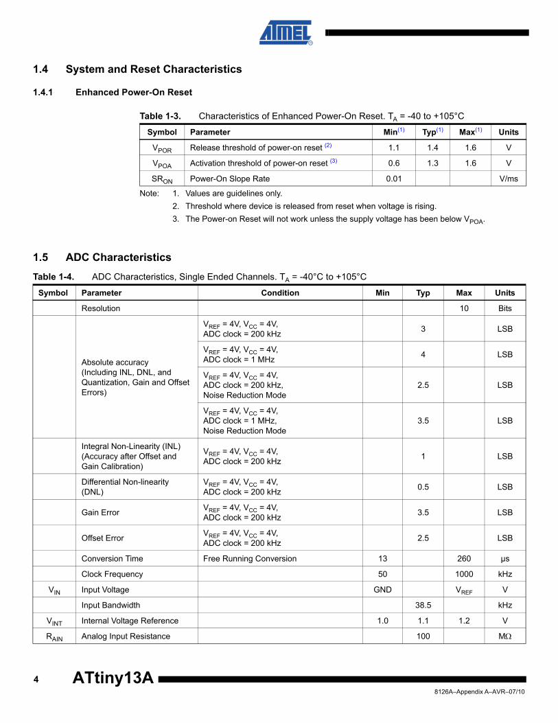
1.4 System and Reset Characteristics
1.4.1 Enhanced Power-On Reset
Note: 1. Values are guidelines only.2. Threshold where device is released from reset when voltage is rising.3. The Power-on Reset will not work unless the supply voltage has been below VPOA.
1.5 ADC Characteristics
Table 1-3. Characteristics of Enhanced Power-On Reset. TA = -40 to +105°C
Symbol Parameter Min(1) Typ(1) Max(1) Units
VPOR Release threshold of power-on reset (2) 1.1 1.4 1.6 V
VPOA Activation threshold of power-on reset (3) 0.6 1.3 1.6 V
SRON Power-On Slope Rate 0.01 V/ms
Table 1-4. ADC Characteristics, Single Ended Channels. TA = -40°C to +105°C
Symbol Parameter Condition Min Typ Max Units
Resolution 10 Bits
Absolute accuracy(Including INL, DNL, and Quantization, Gain and Offset Errors)
VREF = 4V, VCC = 4V,ADC clock = 200 kHz 3 LSB
VREF = 4V, VCC = 4V,ADC clock = 1 MHz 4 LSB
VREF = 4V, VCC = 4V,ADC clock = 200 kHz,Noise Reduction Mode
2.5 LSB
VREF = 4V, VCC = 4V,ADC clock = 1 MHz,Noise Reduction Mode
3.5 LSB
Integral Non-Linearity (INL)(Accuracy after Offset and Gain Calibration)
VREF = 4V, VCC = 4V,ADC clock = 200 kHz 1 LSB
Differential Non-linearity (DNL)
VREF = 4V, VCC = 4V,ADC clock = 200 kHz 0.5 LSB
Gain Error VREF = 4V, VCC = 4V,ADC clock = 200 kHz 3.5 LSB
Offset Error VREF = 4V, VCC = 4V,ADC clock = 200 kHz 2.5 LSB
Conversion Time Free Running Conversion 13 260 µs
Clock Frequency 50 1000 kHz
VIN Input Voltage GND VREF V
Input Bandwidth 38.5 kHz
VINT Internal Voltage Reference 1.0 1.1 1.2 V
RAIN Analog Input Resistance 100 MΩ
48126A–Appendix A–AVR–07/10
ATtiny13A

ATtiny13A
1.6 Analog Comparator Characteristics
Note: All parameters are based on simulation results.
1.7 Serial Programming Characteristics
Note: 1. 2 tCLCL for fck < 12 MHz, 3 tCLCL for fck >= 12 MHz
Table 1-5. Analog Comparator Characteristics, TA = -40°C to +105°C
Symbol Parameter Condition Min Typ Max Units
VAIO Input Offset Voltage VCC = 5V, VIN = VCC / 2 < 10 40 mV
ILAC Input Leakage Current VCC = 5V, VIN = VCC / 2 -50 50 nA
tAPD
Analog Propagation Delay(from saturation to slight overdrive)
VCC = 2.7V 750
nsVCC = 4.0V 500
Analog Propagation Delay(large step change)
VCC = 2.7V 100
VCC = 4.0V 75
tDPD Digital Propagation Delay VCC = 1.8V - 5.5 1 2 CLK
Table 1-6. Serial Programming Characteristics, TA = -40°C to +105°C
Symbol Parameter Condition Min Typ Max Units
1/tCLCL Oscillator FrequencyVCC = 1.8 – 5.5V
0 1 MHz
tCLCL Oscillator Period 1000 ns
1/tCLCL Oscillator FrequencyVCC = 2.7 – 5.5V
0 9.6 MHz
tCLCL Oscillator Period 104 ns
1/tCLCL Oscillator FrequencyVCC = 4.5 – 5.5V
0 20 MHz
tCLCL Oscillator Period 50 ns
tSHSL SCK Pulse Width High
VCC = 1.8 – 5.5V
2 tCLCL(1) ns
tSLSH SCK Pulse Width Low 2 tCLCL(1) ns
tOVSH MOSI Setup to SCK High tCLCL ns
tSHOX MOSI Hold after SCK High 2 tCLCL ns
58126A–Appendix A–AVR–07/10

2. Typical CharacteristicsThe data contained in this section is largely based on simulations and characterization of similardevices in the same process and design methods. Thus, the data should be treated as indica-tions of how the part will behave.
The following charts show typical behavior. These figures are not tested during manufacturing.During characterisation devices are operated at frequencies higher than test limits but they arenot guaranteed to function properly at frequencies higher than the ordering code indicates.
All current consumption measurements are performed with all I/O pins configured as inputs andwith internal pull-ups enabled. Current consumption is a function of several factors such as oper-ating voltage, operating frequency, loading of I/O pins, switching rate of I/O pins, code executedand ambient temperature. The dominating factors are operating voltage and frequency.
A sine wave generator with rail-to-rail output is used as clock source but current consumption inPower-Down mode is independent of clock selection. The difference between current consump-tion in Power-Down mode with Watchdog Timer enabled and Power-Down mode with WatchdogTimer disabled represents the differential current drawn by the Watchdog Timer.
The current drawn from pins with a capacitive load may be estimated (for one pin) as follows:
where VCC = operating voltage, CL = load capacitance and fSW = average switching frequency ofI/O pin.
2.1 Current Consumption in Active Mode
Figure 2-1. Active Supply Current vs. VCC (Internal Calibrated Oscillator, 9.6 MHz)
ICP VCC CL f×× SW≈
ACTIVE SUPPLY CURRENT vs. VCC
INTERNAL OSCILLATOR, 9.6 MHz
105 °C85 °C25 °C
-40 °C
0
1
2
3
4
5
6
1.5 2 2.5 3 3.5 4 4.5 5 5.5
VCC (V)
I CC (
mA
)
68126A–Appendix A–AVR–07/10
ATtiny13A
ATtiny13A
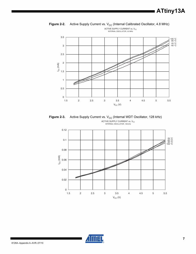
Figure 2-2. Active Supply Current vs. VCC (Internal Calibrated Oscillator, 4.8 MHz)
Figure 2-3. Active Supply Current vs. VCC (Internal WDT Oscillator, 128 kHz)
ACTIVE SUPPLY CURRENT vs. VCC
INTERNAL OSCILLATOR, 4.8 MHz
105 °C85 °C25 °C
-40 °C
0
0.5
1
1.5
2
2.5
3
3.5
1.5 2 2.5 3 3.5 4 4.5 5 5.5
VCC (V)
I CC (
mA
)
ACTIVE SUPPLY CURRENT vs. VCC
INTERNAL OSCILLATOR, 128 kHz
105 °C85 °C
25 °C-40 °C
0
0.02
0.04
0.06
0.08
0.1
0.12
1.5 2 2.5 3 3.5 4 4.5 5 5.5
VCC (V)
I CC (
mA
)
78126A–Appendix A–AVR–07/10
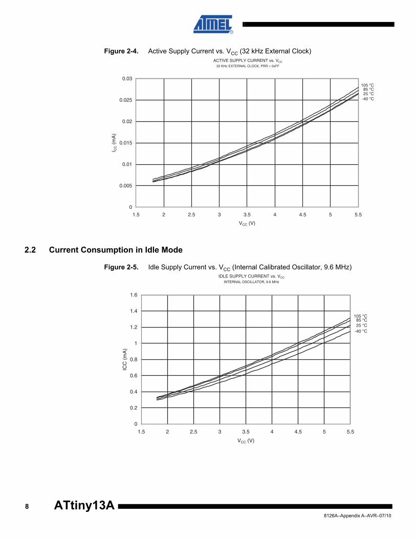
Figure 2-4. Active Supply Current vs. VCC (32 kHz External Clock)
2.2 Current Consumption in Idle Mode
Figure 2-5. Idle Supply Current vs. VCC (Internal Calibrated Oscillator, 9.6 MHz)
ACTIVE SUPPLY CURRENT vs. VCC
32 KHz EXTERNAL CLOCK, PRR = 0xFF
105 °C85 °C25 °C
-40 °C
0
0.005
0.01
0.015
0.02
0.025
0.03
1.5 2 2.5 3 3.5 4 4.5 5 5.5
VCC (V)
I CC (
mA
)
IDLE SUPPLY CURRENT vs. VCC
INTERNAL OSCILLATOR, 9.6 MHz
105 °C85 °C25 °C
-40 °C
0
0.2
0.4
0.6
0.8
1
1.2
1.4
1.6
1.5 2 2.5 3 3.5 4 4.5 5 5.5
VCC (V)
ICC
(m
A)
88126A–Appendix A–AVR–07/10
ATtiny13A

ATtiny13A
Figure 2-6. Idle Supply Current vs. VCC (Internal Calibrated Oscillator, 4.8 MHz)
Figure 2-7. Idle Supply Current vs. VCC (Internal Oscillator, 128 kHz)
IDLE SUPPLY CURRENT vs. VCC
INTERNAL OSCILLATOR, 4.8 MHz
105 °C85 °C
25 °C
-40 °C
0
0.1
0.2
0.3
0.4
0.5
0.6
0.7
1.5 2 2.5 3 3.5 4 4.5 5 5.5
VCC (V)
I CC (
mA
)
IDLE SUPPLY CURRENT vs. VCC
INTERNAL OSCILLATOR, 128 kHz
105 °C85 °C
25 °C-40 °C
0
0.005
0.01
0.015
0.02
0.025
1.5 2 2.5 3 3.5 4 4.5 5 5.5
VCC (V)
I CC (
mA
)
98126A–Appendix A–AVR–07/10

Figure 2-8. Idle Supply Current vs. VCC (32 kHz External Clock)
2.3 Current Consumption in Power-Down Mode
Figure 2-9. Power-Down Supply Current vs. VCC (Watchdog Timer Disabled)
IDLE SUPPLY CURRENT vs. VCC
32 KHz EXTERNAL OSCILLATOR, PRR=0xFF
105 °C
85 °C
25 °C-40 °C
0
0.001
0.002
0.003
0.004
0.005
0.006
1.5 2 2.5 3 3.5 4 4.5 5 5.5
VCC (V)
I CC (
mA
)
POWER-DOWN SUPPLY CURRENT vs. VCC
WATCHDOG TIMER DISABLED
105 °C
85 °C
25 °C
-40 °C
0
0.2
0.4
0.6
0.8
1
1.2
1.4
1.6
1.5 2 2.5 3 3.5 4 4.5 5 5.5
VCC (V)
I CC (
uA)
108126A–Appendix A–AVR–07/10
ATtiny13A
ATtiny13A
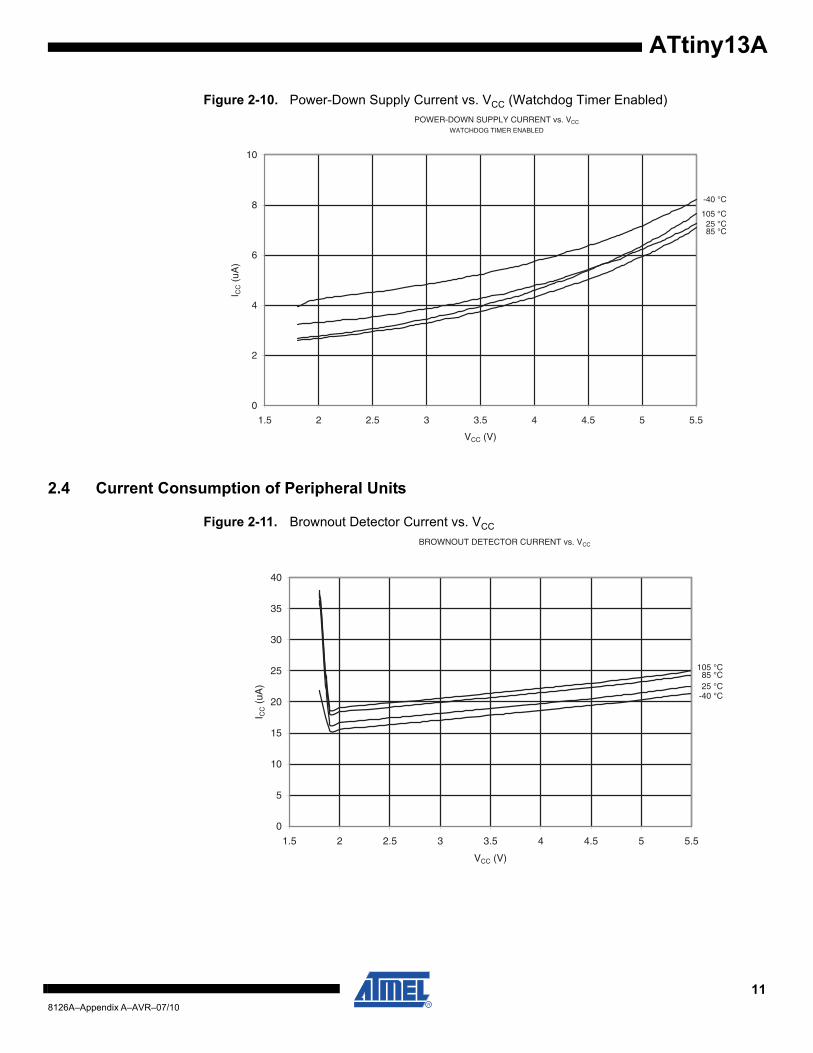
Figure 2-10. Power-Down Supply Current vs. VCC (Watchdog Timer Enabled)
2.4 Current Consumption of Peripheral Units
Figure 2-11. Brownout Detector Current vs. VCC
POWER-DOWN SUPPLY CURRENT vs. VCC
WATCHDOG TIMER ENABLED
105 °C
85 °C25 °C
-40 °C
0
2
4
6
8
10
1.5 2 2.5 3 3.5 4 4.5 5 5.5
VCC (V)
I CC (
uA)
BROWNOUT DETECTOR CURRENT vs. VCC
105 °C85 °C25 °C
-40 °C
0
5
10
15
20
25
30
35
40
1.5 2 2.5 3 3.5 4 4.5 5 5.5
VCC (V)
I CC (
uA)
118126A–Appendix A–AVR–07/10
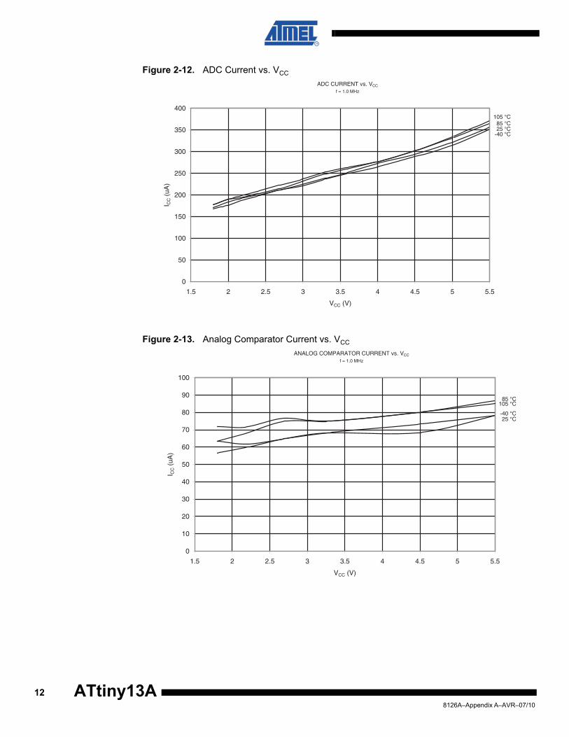
Figure 2-12. ADC Current vs. VCC
Figure 2-13. Analog Comparator Current vs. VCC
ADC CURRENT vs. VCC
f = 1.0 MHz
-40 °C25 °C85 °C
105 °C
0
50
100
150
200
250
300
350
400
1.5 2 2.5 3 3.5 4 4.5 5 5.5
VCC (V)
I CC (
uA)
ANALOG COMPARATOR CURRENT vs. VCC
f = 1.0 MHz
-40 °C25 °C
85 °C105 °C
0
10
20
30
40
50
60
70
80
90
100
1.5 2 2.5 3 3.5 4 4.5 5 5.5
VCC (V)
I CC (
uA)
128126A–Appendix A–AVR–07/10
ATtiny13A

ATtiny13A
Figure 2-14. Programming Current vs. VCC
2.5 Pull-up Resistors
Figure 2-15. Pull-up Resistor Current vs. Input Voltage (I/O Pin, VCC = 1.8V)
PROGRAMMING CURRENT vs. VCC
105 °C85 °C
25 °C
-40 °C
0
1000
2000
3000
4000
5000
6000
7000
8000
9000
1.5 2 2.5 3 3.5 4 4.5 5 5.5
VCC (V)
I CC (
uA)
I/O PIN PULL-UP RESISTOR CURRENT vs. INPUT VOLTAGE
105 °C85 °C25 °C
-40 °C0
10
20
30
40
50
60
0 0.5 1 1.5 2
VOP (V)
I OP (
uA)
138126A–Appendix A–AVR–07/10

Figure 2-16. Pull-up Resistor Current vs. Input Voltage (I/O Pin, VCC = 3V)
Figure 2-17. Pull-up Resistor Current vs. Input Voltage (I/O Pin, VCC = 5V)
85 °C25 °C
-40 °C105 °C
I/O PIN PULL-UP RESISTOR CURRENT vs. INPUT VOLTAGEVCC = 3V
0
10
20
30
40
50
60
70
80
90
100
0 0,5 1 1,5 2 2,5 3 3,5
VOP (V)
I OP (u
A)
105 °C85 °C25 °C
-40 °C
I/O PIN PULL-UP RESISTOR CURRENT vs. INPUT VOLTAGE
0
20
40
60
80
100
120
140
160
0 1 2 3 4 5 6
VOP (V)
I OP (
uA)
148126A–Appendix A–AVR–07/10
ATtiny13A
ATtiny13A
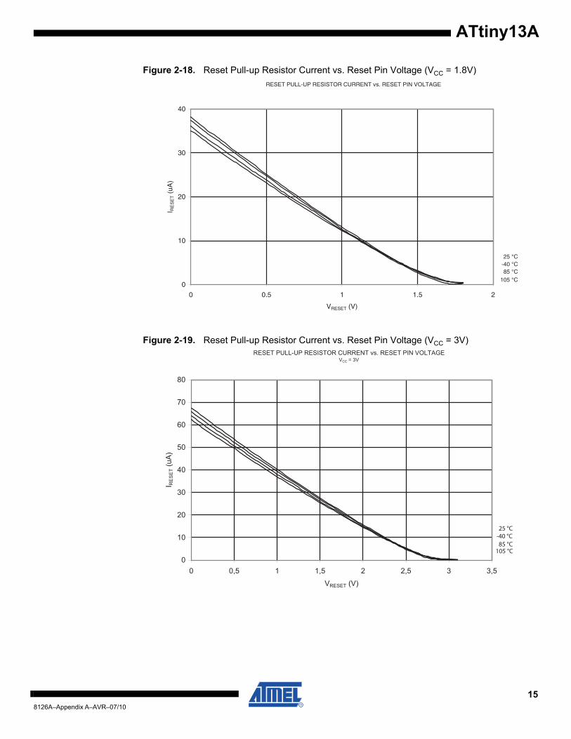
Figure 2-18. Reset Pull-up Resistor Current vs. Reset Pin Voltage (VCC = 1.8V)
Figure 2-19. Reset Pull-up Resistor Current vs. Reset Pin Voltage (VCC = 3V)
RESET PULL-UP RESISTOR CURRENT vs. RESET PIN VOLTAGE
105 °C85 °C
25 °C-40 °C
0
10
20
30
40
0 0.5 1 1.5 2
VRESET (V)
I RE
SE
T (
uA)
85 °C
25 °C-40 °C
105 °C
RESET PULL-UP RESISTOR CURRENT vs. RESET PIN VOLTAGEVCC = 3V
0
10
20
30
40
50
60
70
80
0 0,5 1 1,5 2 2,5 3 3,5
VRESET (V)
I RE
SE
T (u
A)
158126A–Appendix A–AVR–07/10
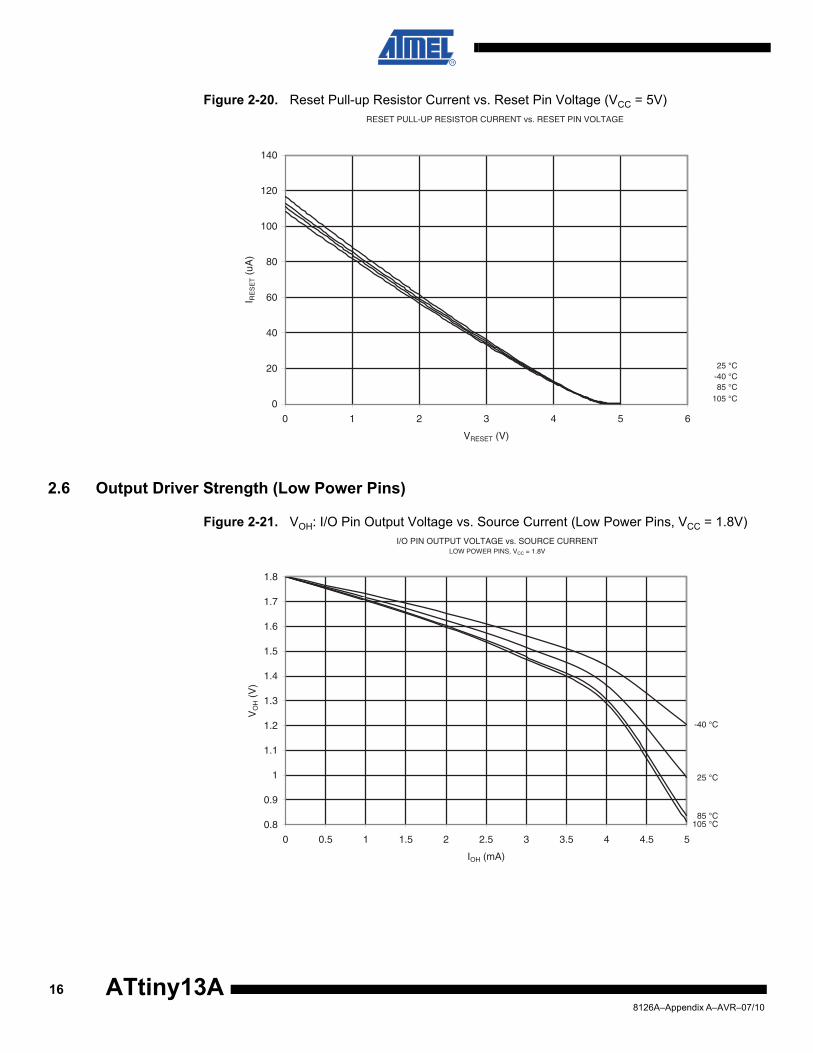
Figure 2-20. Reset Pull-up Resistor Current vs. Reset Pin Voltage (VCC = 5V)
2.6 Output Driver Strength (Low Power Pins)
Figure 2-21. VOH: I/O Pin Output Voltage vs. Source Current (Low Power Pins, VCC = 1.8V)
105 °C85 °C
25 °C-40 °C
RESET PULL-UP RESISTOR CURRENT vs. RESET PIN VOLTAGE
0
20
40
60
80
100
120
140
0 1 2 3 4 5 6
VRESET (V)
I RE
SE
T (
uA)
I/O PIN OUTPUT VOLTAGE vs. SOURCE CURRENTLOW POWER PINS, VCC = 1.8V
105 °C85 °C
25 °C
-40 °C
0.8
0.9
1
1.1
1.2
1.3
1.4
1.5
1.6
1.7
1.8
0 0.5 1 1.5 2 2.5 3 3.5 4 4.5 5
IOH (mA)
VO
H (
V)
168126A–Appendix A–AVR–07/10
ATtiny13A

ATtiny13A
Figure 2-22. VOH: I/O Pin Output Voltage vs. Source Current (Low Power Pins, VCC = 3V)
Figure 2-23. VOH: I/O Pin Output Voltage vs. Source Current (Low Power Pins, VCC = 5V)
I/O PIN OUTPUT VOLTAGE vs. SOURCE CURRENTLOW POWER PINS, VCC = 3V
105 °C85 °C
25 °C
-40 °C
2.3
2.4
2.5
2.6
2.7
2.8
2.9
3
0 1 2 3 4 5 6 7 8 9 10
IOH (mA)
VO
H (
V)
I/O PIN OUTPUT VOLTAGE vs. SOURCE CURRENTLOW POWER PINS, VCC = 5V
105 °C85 °C
25 °C
-40 °C
4
4.2
4.4
4.6
4.8
5
0 2 4 6 8 10 12 14 16 18 20
IOH (mA)
VO
H (
V)
178126A–Appendix A–AVR–07/10
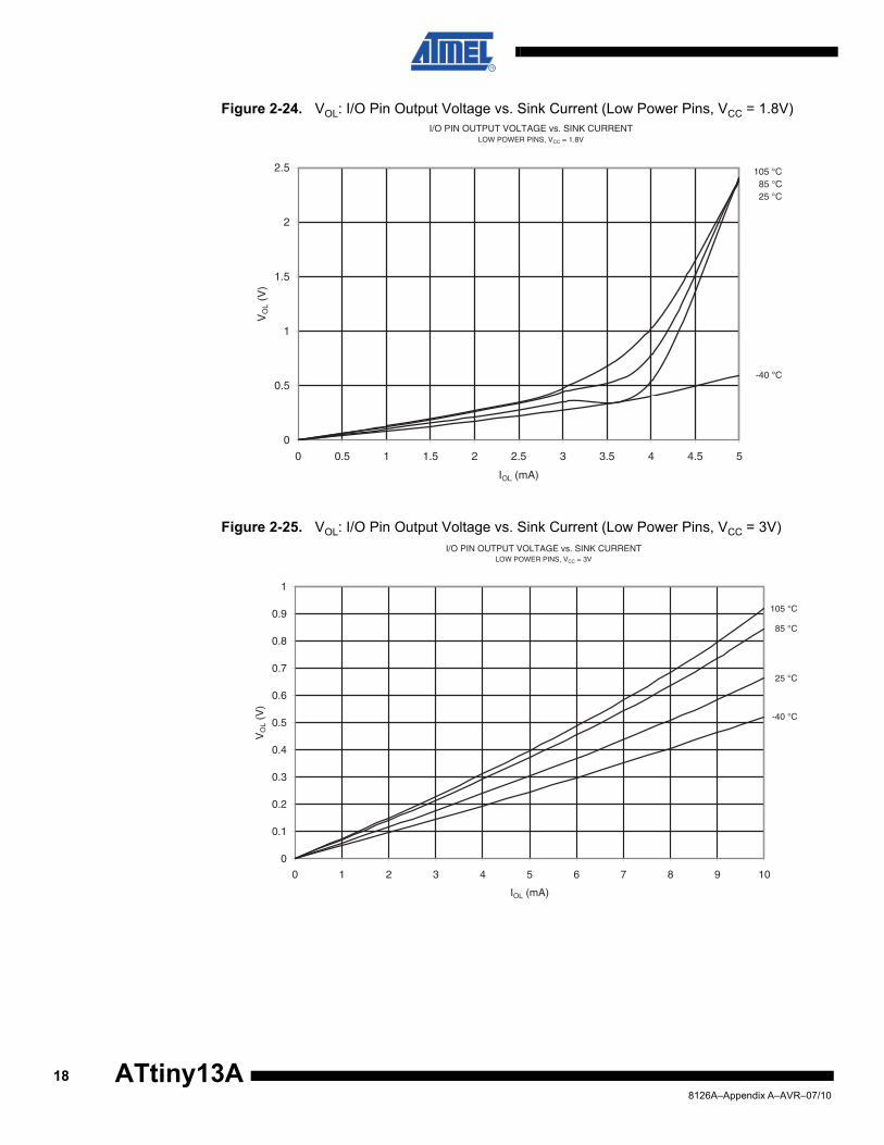
Figure 2-24. VOL: I/O Pin Output Voltage vs. Sink Current (Low Power Pins, VCC = 1.8V)
Figure 2-25. VOL: I/O Pin Output Voltage vs. Sink Current (Low Power Pins, VCC = 3V)
I/O PIN OUTPUT VOLTAGE vs. SINK CURRENTLOW POWER PINS, VCC = 1.8V
105 °C85 °C25 °C
-40 °C
0
0.5
1
1.5
2
2.5
0 0.5 1 1.5 2 2.5 3 3.5 4 4.5 5
IOL (mA)
VO
L (V
)
I/O PIN OUTPUT VOLTAGE vs. SINK CURRENTLOW POWER PINS, VCC = 3V
105 °C
85 °C
25 °C
-40 °C
0
0.1
0.2
0.3
0.4
0.5
0.6
0.7
0.8
0.9
1
0 1 2 3 4 5 6 7 8 9 10
IOL (mA)
VO
L (V
)
188126A–Appendix A–AVR–07/10
ATtiny13A
ATtiny13A
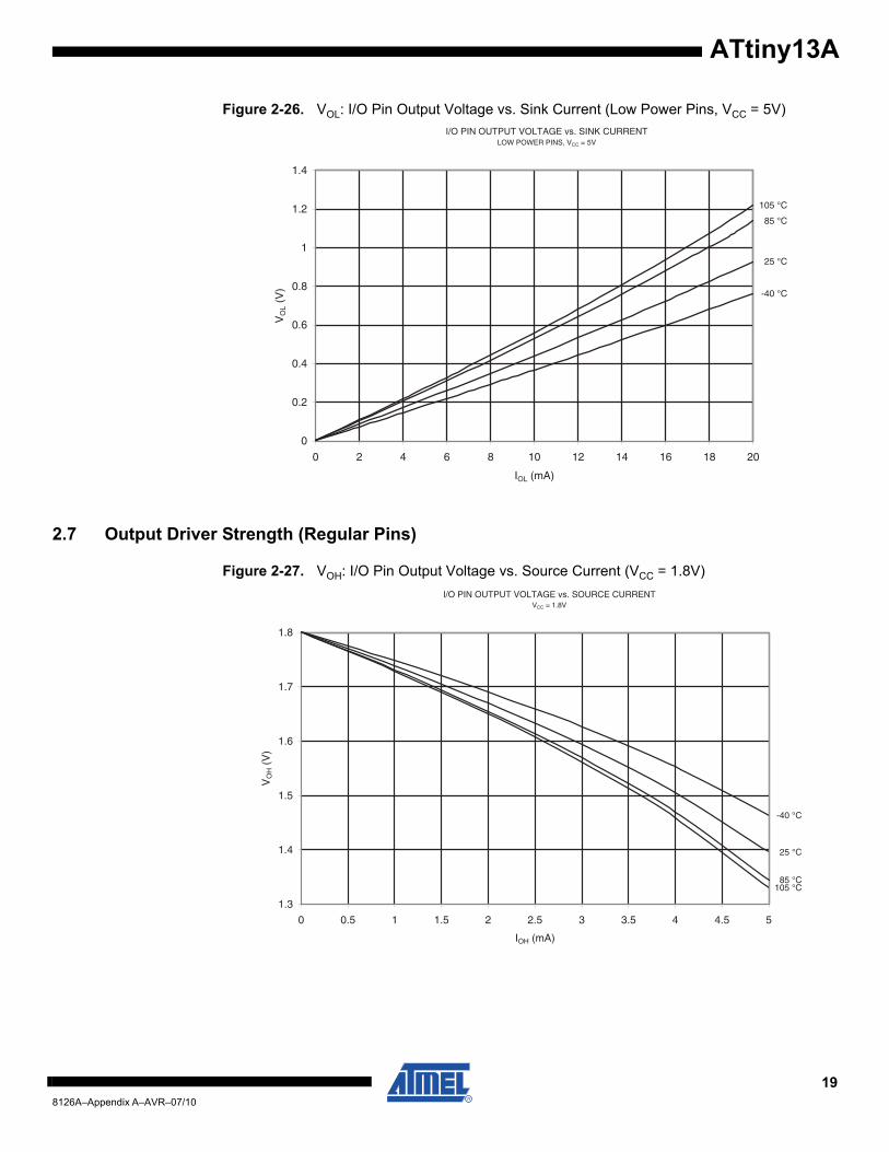
Figure 2-26. VOL: I/O Pin Output Voltage vs. Sink Current (Low Power Pins, VCC = 5V)
2.7 Output Driver Strength (Regular Pins)
Figure 2-27. VOH: I/O Pin Output Voltage vs. Source Current (VCC = 1.8V)
I/O PIN OUTPUT VOLTAGE vs. SINK CURRENTLOW POWER PINS, VCC = 5V
105 °C
85 °C
25 °C
-40 °C
0
0.2
0.4
0.6
0.8
1
1.2
1.4
0 2 4 6 8 10 12 14 16 18 20
IOL (mA)
VO
L (V
)
I/O PIN OUTPUT VOLTAGE vs. SOURCE CURRENTVCC = 1.8V
105 °C85 °C
25 °C
-40 °C
1.3
1.4
1.5
1.6
1.7
1.8
0 0.5 1 1.5 2 2.5 3 3.5 4 4.5 5
IOH (mA)
VO
H (
V)
198126A–Appendix A–AVR–07/10

Figure 2-28. VOH: I/O Pin Output Voltage vs. Source Current (VCC = 3V)
Figure 2-29. VOH: I/O Pin Output Voltage vs. Source Current (VCC = 5V)
I/O PIN OUTPUT VOLTAGE vs. SOURCE CURRENTVCC = 3V
105 °C85 °C
25 °C
-40 °C
2.5
2.6
2.7
2.8
2.9
3
0 1 2 3 4 5 6 7 8 9 10
IOH (mA)
VO
H (
V)
I/O PIN OUTPUT VOLTAGE vs. SOURCE CURRENTVCC = 5V
105 °C85 °C
25 °C
-40 °C
4.2
4.4
4.6
4.8
5
0 2 4 6 8 10 12 14 16 18 20
IOH (mA)
VO
H (
V)
208126A–Appendix A–AVR–07/10
ATtiny13A
ATtiny13A
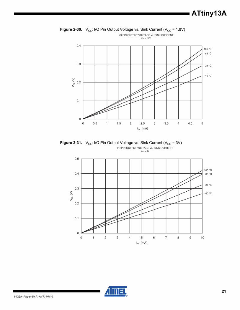
Figure 2-30. VOL: I/O Pin Output Voltage vs. Sink Current (VCC = 1.8V)
Figure 2-31. VOL: I/O Pin Output Voltage vs. Sink Current (VCC = 3V)
I/O PIN OUTPUT VOLTAGE vs. SINK CURRENTVCC = 1.8V
105 °C
85 °C
25 °C
-40 °C
0
0.1
0.2
0.3
0.4
0 0.5 1 1.5 2 2.5 3 3.5 4 4.5 5
IOL (mA)
VO
L (V
)
I/O PIN OUTPUT VOLTAGE vs. SINK CURRENTVCC = 3V
105 °C
85 °C
25 °C
-40 °C
0
0.1
0.2
0.3
0.4
0.5
0 1 2 3 4 5 6 7 8 9 10
IOL (mA)
VO
L (V
)
218126A–Appendix A–AVR–07/10
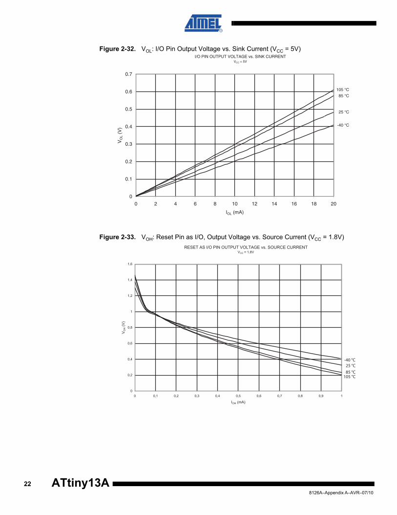
Figure 2-32. VOL: I/O Pin Output Voltage vs. Sink Current (VCC = 5V)
Figure 2-33. VOH: Reset Pin as I/O, Output Voltage vs. Source Current (VCC = 1.8V)
I/O PIN OUTPUT VOLTAGE vs. SINK CURRENTVCC = 5V
105 °C
85 °C
25 °C
-40 °C
0
0.1
0.2
0.3
0.4
0.5
0.6
0.7
0 2 4 6 8 10 12 14 16 18 20
IOL (mA)
VO
L (V
)
85 °C105 °C
25 °C-40 °C
RESET AS I/O PIN OUTPUT VOLTAGE vs. SOURCE CURRENTVCC = 1.8V
0
0,2
0,4
0,6
0,8
1
1,2
1,4
1,6
0 0,1 0,2 0,3 0,4 0,5 0,6 0,7 0,8 0,9 1
IOH (mA)
VO
H (V
)
228126A–Appendix A–AVR–07/10
ATtiny13A

ATtiny13A
Figure 2-34. VOH: Reset Pin as I/O, Output Voltage vs. Source Current (VCC = 3V)
Figure 2-35. VOH: Reset Pin as I/O, Output Voltage vs. Source Current (VCC = 5V)
85 °C105 °C
25 °C-40 °C
RESET AS I/O PIN OUTPUT VOLTAGE vs. SOURCE CURRENTVCC = 3V
0
0,5
1
1,5
2
2,5
3
3,5
4
4,5
0 0,1 0,2 0,3 0,4 0,5 0,6 0,7 0,8 0,9 1
IOH (mA)
VO
H (V
)
85 °C105 °C
25 °C-40 °C
RESET AS I/O PIN OUTPUT VOLTAGE vs. SOURCE CURRENTVCC = 5V
0
0,5
1
1,5
2
2,5
3
3,5
4
4,5
0 0,1 0,2 0,3 0,4 0,5 0,6 0,7 0,8 0,9 1
IOH (mA)
VO
H (V
)
238126A–Appendix A–AVR–07/10
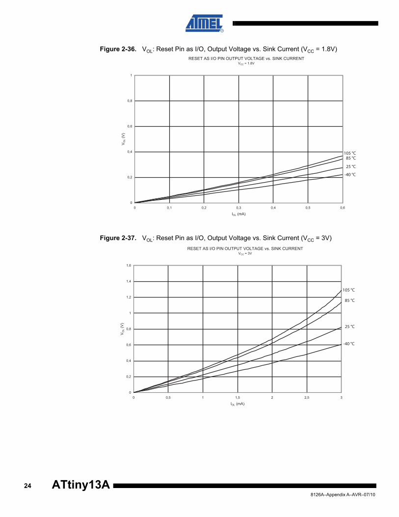
Figure 2-36. VOL: Reset Pin as I/O, Output Voltage vs. Sink Current (VCC = 1.8V)
Figure 2-37. VOL: Reset Pin as I/O, Output Voltage vs. Sink Current (VCC = 3V)
85 °C
25 °C
-40 °C
RESET AS I/O PIN OUTPUT VOLTAGE vs. SINK CURRENTVCC = 1.8V
0
0,2
0,4
0,6
0,8
1
0 0,1 0,2 0,3 0,4 0,5 0,6
IOL (mA)
VO
L (V
)
105 °C
85 °C
105 °C
25 °C
-40 °C
RESET AS I/O PIN OUTPUT VOLTAGE vs. SINK CURRENTVCC = 3V
0
0,2
0,4
0,6
0,8
1
1,2
1,4
1,6
0 0,5 1 1,5 2 2,5 3
IOL (mA)
VO
L (V
)
248126A–Appendix A–AVR–07/10
ATtiny13A

ATtiny13A
Figure 2-38. VOL: Reset Pin as I/O, Output Voltage vs. Sink Current (VCC = 5V)
2.8 Input Thresholds and Hysteresis (for I/O Ports)
Figure 2-39. VIH: Input Threshold Voltage vs. VCC (I/O Pin, Read as '1')
RESET AS I/O PIN OUTPUT VOLTAGE vs. SINK CURRENTVCC = 5V
0
0,2
0,4
0,6
0,8
1
1,2
1,4
1,6
0 0,5 1 1,5 2 2,5 3 3,5 4 4,5 5
IOL (mA)
VO
L (V
)85 °C
25 °C
-40 °C
105 °C
I/O PIN INPUT THRESHOLD VOLTAGE vs. VCCVIH, I/O PIN READ AS '1'
105 °C85 °C25 °C
-40 °C
0
0.5
1
1.5
2
2.5
3
1.5 2 2.5 3 3.5 4 4.5 5 5.5
VCC (V)
Thr
esho
ld (
V)
258126A–Appendix A–AVR–07/10

Figure 2-40. VIL: Input Threshold Voltage vs. VCC (I/O Pin, Read as '0')
Figure 2-41. VIH-VIL: Input Hysteresis vs. VCC (I/O Pin)
I/O PIN INPUT THRESHOLD VOLTAGE vs. VCCVIL, I/O PIN READ AS '0'
105 °C85 °C25 °C
-40 °C
0
0.5
1
1.5
2
2.5
1.5 2 2.5 3 3.5 4 4.5 5 5.5
VCC (V)
Thr
esho
ld (
V)
I/O PIN INPUT HYSTERESIS vs. VCC
105 °C
85 °C
25 °C
-40 °C
0
0.1
0.2
0.3
0.4
0.5
0.6
1.5 2 2.5 3 3.5 4 4.5 5 5.5
VCC (V)
Inpu
t Hys
tere
sis
(V)
268126A–Appendix A–AVR–07/10
ATtiny13A
ATtiny13A
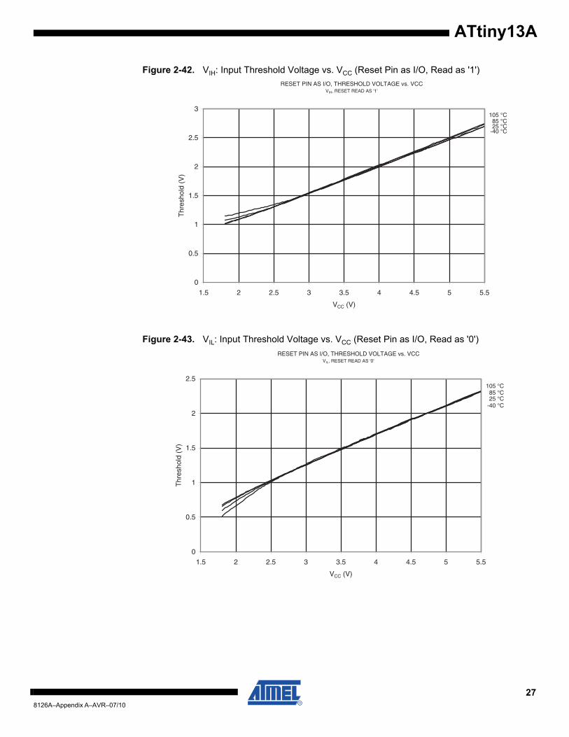
Figure 2-42. VIH: Input Threshold Voltage vs. VCC (Reset Pin as I/O, Read as '1')
Figure 2-43. VIL: Input Threshold Voltage vs. VCC (Reset Pin as I/O, Read as '0')
RESET PIN AS I/O, THRESHOLD VOLTAGE vs. VCCVIH, RESET READ AS '1'
105 °C85 °C25 °C
-40 °C
0
0.5
1
1.5
2
2.5
3
1.5 2 2.5 3 3.5 4 4.5 5 5.5
VCC (V)
Thr
esho
ld (
V)
RESET PIN AS I/O, THRESHOLD VOLTAGE vs. VCCVIL, RESET READ AS '0'
105 °C85 °C25 °C
-40 °C
0
0.5
1
1.5
2
2.5
1.5 2 2.5 3 3.5 4 4.5 5 5.5
VCC (V)
Thr
esho
ld (
V)
278126A–Appendix A–AVR–07/10

Figure 2-44. VIH-VIL: Input Hysteresis vs. VCC (Reset Pin as I/O)
2.9 BOD, Bandgap and Reset
Figure 2-45. BOD Thresholds vs. Temperature (BODLEVEL is 4.3V)
RESET PIN AS IO, INPUT HYSTERESIS vs. VCC
105 °C85 °C25 °C
-40 °C
0
0.1
0.2
0.3
0.4
0.5
0.6
0.7
0.8
0.9
1
1.5 2 2.5 3 3.5 4 4.5 5 5.5
V CC (V)
Inpu
t Hys
tere
sis
(V)
RISING VCC
FALLING VCC
BOD THRESHOLDS vs. TEMPERATUREBODLEVEL = 4.3V
4.26
4.28
4.3
4.32
4.34
4.36
4.38
4.4
-40 -20 0 20 40 60 80 100 120
Temperature (C)
Thr
esho
ld (
V)
288126A–Appendix A–AVR–07/10
ATtiny13A
ATtiny13A
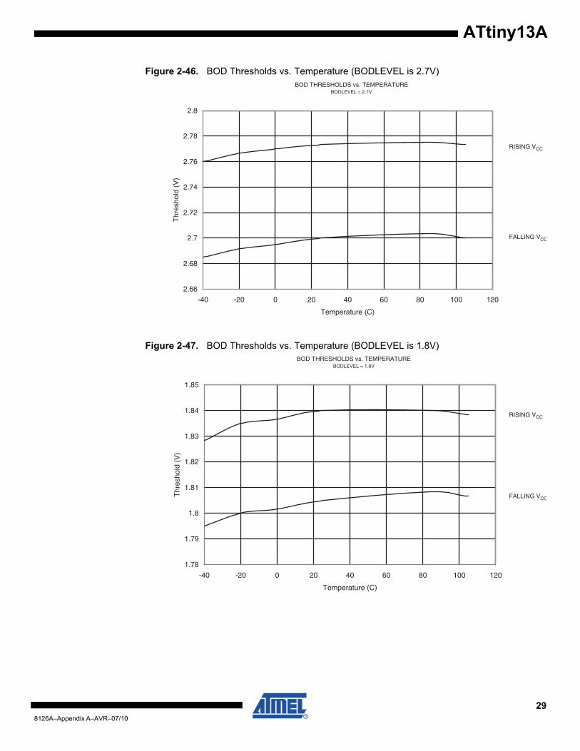
Figure 2-46. BOD Thresholds vs. Temperature (BODLEVEL is 2.7V)
Figure 2-47. BOD Thresholds vs. Temperature (BODLEVEL is 1.8V)
RISING VCC
FALLING VCC
BOD THRESHOLDS vs. TEMPERATUREBODLEVEL = 2.7V
2.66
2.68
2.7
2.72
2.74
2.76
2.78
2.8
-40 -20 0 20 40 60 80 100 120
Temperature (C)
Thr
esho
ld (
V)
BOD THRESHOLDS vs. TEMPERATUREBODLEVEL = 1.8V
RISING VCC
FALLING VCC
1.78
1.79
1.8
1.81
1.82
1.83
1.84
1.85
-40 -20 0 20 40 60 80 100 120
Temperature (C)
Thr
esho
ld (
V)
298126A–Appendix A–AVR–07/10

Figure 2-48. Bandgap Voltage vs. VCC
Figure 2-49. VIH: Reset Input Threshold Voltage vs. VCC (Reset Pin Read as '1')
BANDGAP VOLTAGE vs. VCC
105 °C85 °C25 °C
-40 °C
1.08
1.09
1.1
1.11
1.12
1.13
1.14
1.5 2 2.5 3 3.5 4 4.5 5 5.5
VCC (V)
Ban
dgap
Vol
tage
(V
)
RESET INPUT THRESHOLD VOLTAGE vs. VCCVIH, PIN READ AS '1'
105 °C85 °C25 °C
-40 °C
0
0.5
1
1.5
2
2.5
1.5 2 2.5 3 3.5 4 4.5 5 5.5
VCC (V)
Thr
esho
ld (
V)
308126A–Appendix A–AVR–07/10
ATtiny13A
ATtiny13A
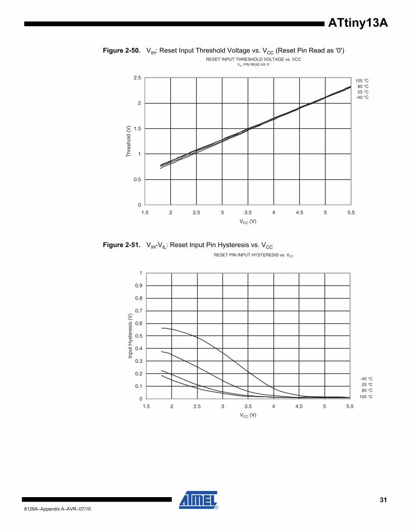
Figure 2-50. VIH: Reset Input Threshold Voltage vs. VCC (Reset Pin Read as '0')
Figure 2-51. VIH-VIL: Reset Input Pin Hysteresis vs. VCC
RESET INPUT THRESHOLD VOLTAGE vs. VCCVIL, PIN READ AS '0'
105 °C85 °C25 °C
-40 °C
0
0.5
1
1.5
2
2.5
1.5 2 2.5 3 3.5 4 4.5 5 5.5
VCC (V)
Thr
esho
ld (
V)
RESET PIN INPUT HYSTERESIS vs. VCC
105 °C
85 °C25 °C
-40 °C
0
0.1
0.2
0.3
0.4
0.5
0.6
0.7
0.8
0.9
1
1.5 2 2.5 3 3.5 4 4.5 5 5.5
VCC (V)
Inpu
t Hys
tere
sis
(V)
318126A–Appendix A–AVR–07/10

Figure 2-52. Minimum Reset Pulse Width vs. VCC
2.10 Internal Oscillator Speed
Figure 2-53. Calibrated 9.6 MHz Oscillator Frequency vs. Temperature
MINIMUM RESET PULSE WIDTH vs. VCC
105 °C85 °C25 °C
-40 °C
0
200
400
600
800
1000
1200
1400
1600
1800
1.5 2 2.5 3 3.5 4 4.5 5 5.5
VCC (V)
Pul
sew
idth
(ns
)
CALIBRATED 9.6MHz OSCILLATOR FREQUENCY vs. TEMPERATURE
5.5 V4.5 V2.7 V1.8 V
9
9.2
9.4
9.6
9.8
10
10.2
-40 -20 0 20 40 60 80 100 120
Temperature
Fre
quen
cy (
MH
z)
328126A–Appendix A–AVR–07/10
ATtiny13A
ATtiny13A
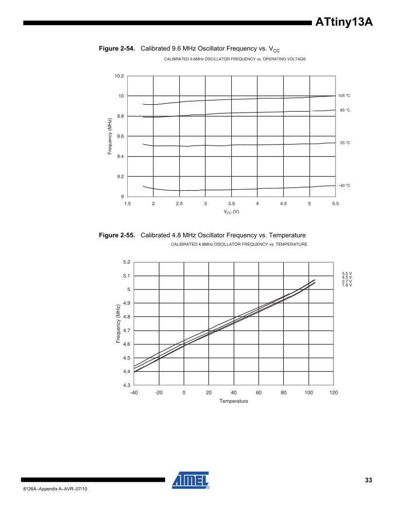
Figure 2-54. Calibrated 9.6 MHz Oscillator Frequency vs. VCC
Figure 2-55. Calibrated 4.8 MHz Oscillator Frequency vs. Temperature
CALIBRATED 9.6MHz OSCILLATOR FREQUENCY vs. OPERATING VOLTAGE
105 °C
85 °C
25 °C
-40 °C
9
9.2
9.4
9.6
9.8
10
10.2
1.5 2 2.5 3 3.5 4 4.5 5 5.5
VCC (V)
Fre
quen
cy (
MH
z)
CALIBRATED 4.8MHz OSCILLATOR FREQUENCY vs. TEMPERATURE
5.5 V4.5 V2.7 V1.8 V
4.3
4.4
4.5
4.6
4.7
4.8
4.9
5
5.1
5.2
-40 -20 0 20 40 60 80 100 120
Temperature
Fre
quen
cy (
MH
z)
338126A–Appendix A–AVR–07/10
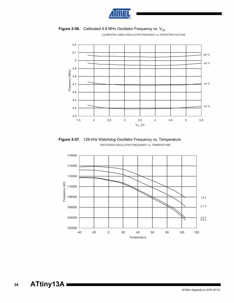
Figure 2-56. Calibrated 4.8 MHz Oscillator Frequency vs. VCC
Figure 2-57. 128 kHz Watchdog Oscillator Frequency vs. Temperature
CALIBRATED 4.8MHz OSCILLATOR FREQUENCY vs. OPERATING VOLTAGE
105 °C
85 °C
25 °C
-40 °C
4.3
4.4
4.5
4.6
4.7
4.8
4.9
5
5.1
5.2
1.5 2 2.5 3 3.5 4 4.5 5 5.5
VCC (V)
Fre
quen
cy (
MH
z)
WATCHDOG OSCILLATOR FREQUENCY vs. TEMPERATURE
5.5 V4.5 V
2.7 V
1.8 V
102000
104000
106000
108000
110000
112000
114000
116000
-40 -20 0 20 40 60 80 100 120
Temperature
Fre
quen
cy (
kH)
348126A–Appendix A–AVR–07/10
ATtiny13A

ATtiny13A
Figure 2-58. 128 kHz Watchdog Oscillator Frequency vs. VCC
WATCHDOG OSCILLATOR FREQUENCY vs. OPERATING VOLTAGE
105 °C
85 °C
25 °C
-40 °C
102000
104000
106000
108000
110000
112000
114000
116000
1.5 2 2.5 3 3.5 4 4.5 5 5.5
VCC (V)
Fre
quen
cy (
Hz)
358126A–Appendix A–AVR–07/10
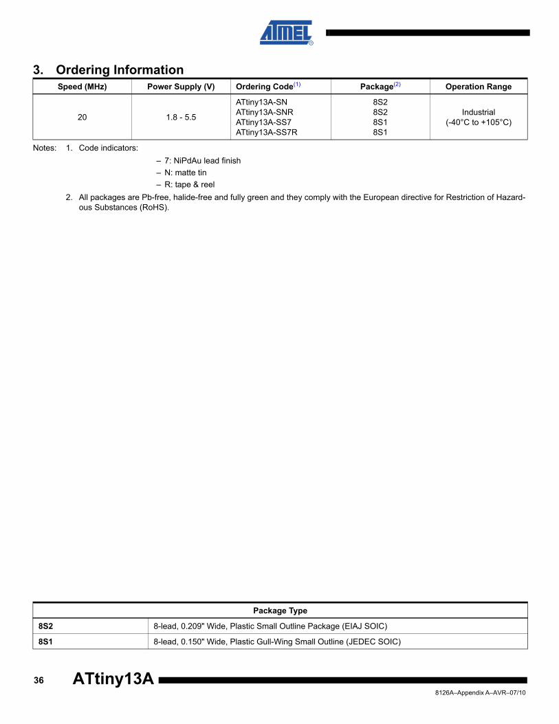
3. Ordering Information
Notes: 1. Code indicators:– 7: NiPdAu lead finish– N: matte tin– R: tape & reel
2. All packages are Pb-free, halide-free and fully green and they comply with the European directive for Restriction of Hazard-ous Substances (RoHS).
Speed (MHz) Power Supply (V) Ordering Code(1) Package(2) Operation Range
20 1.8 - 5.5
ATtiny13A-SNATtiny13A-SNRATtiny13A-SS7ATtiny13A-SS7R
8S28S28S18S1
Industrial(-40°C to +105°C)
Package Type
8S2 8-lead, 0.209" Wide, Plastic Small Outline Package (EIAJ SOIC)
8S1 8-lead, 0.150" Wide, Plastic Gull-Wing Small Outline (JEDEC SOIC)
368126A–Appendix A–AVR–07/10
ATtiny13A

ATtiny13A
4. Revision History
Revision No. History
8126A–Appendix A–AVR–07/10 8126-Appendix A rev A, initial revision
378126A–Appendix A–AVR–07/10

8126A–Appendix A–AVR–07/10
© 2010 Atmel Corporation. All rights reserved. Atmel®, logo and combinations thereof, AVR® and others are registered trademarks or trade-marks of Atmel Corporation or its subsidiaries. Other terms and product names may be trademarks of others.
Headquarters International
Atmel Corporation2325 Orchard ParkwaySan Jose, CA 95131USATel: 1(408) 441-0311Fax: 1(408) 487-2600
Atmel AsiaUnit 1-5 & 16, 19/FBEA Tower, Millennium City 5418 Kwun Tong RoadKwun Tong, KowloonHong KongTel: (852) 2245-6100Fax: (852) 2722-1369
Atmel EuropeLe Krebs8, Rue Jean-Pierre TimbaudBP 30978054 Saint-Quentin-en-Yvelines CedexFranceTel: (33) 1-30-60-70-00 Fax: (33) 1-30-60-71-11
Atmel Japan9F, Tonetsu Shinkawa Bldg.1-24-8 ShinkawaChuo-ku, Tokyo 104-0033JapanTel: (81) 3-3523-3551Fax: (81) 3-3523-7581
Product Contact
Web Sitewww.atmel.com
Technical [email protected]
Sales Contactwww.atmel.com/contacts
Literature Requestswww.atmel.com/literature
Disclaimer: The information in this document is provided in connection with Atmel products. No license, express or implied, by estoppel or otherwise, to anyintellectual property right is granted by this document or in connection with the sale of Atmel products. EXCEPT AS SET FORTH IN ATMEL’S TERMS AND CONDI-TIONS OF SALE LOCATED ON ATMEL’S WEB SITE, ATMEL ASSUMES NO LIABILITY WHATSOEVER AND DISCLAIMS ANY EXPRESS, IMPLIED OR STATUTORYWARRANTY RELATING TO ITS PRODUCTS INCLUDING, BUT NOT LIMITED TO, THE IMPLIED WARRANTY OF MERCHANTABILITY, FITNESS FOR A PARTICULARPURPOSE, OR NON-INFRINGEMENT. IN NO EVENT SHALL ATMEL BE LIABLE FOR ANY DIRECT, INDIRECT, CONSEQUENTIAL, PUNITIVE, SPECIAL OR INCIDEN-TAL DAMAGES (INCLUDING, WITHOUT LIMITATION, DAMAGES FOR LOSS OF PROFITS, BUSINESS INTERRUPTION, OR LOSS OF INFORMATION) ARISING OUTOF THE USE OR INABILITY TO USE THIS DOCUMENT, EVEN IF ATMEL HAS BEEN ADVISED OF THE POSSIBILITY OF SUCH DAMAGES. Atmel makes norepresentations or warranties with respect to the accuracy or completeness of the contents of this document and reserves the right to make changes to specificationsand product descriptions at any time without notice. Atmel does not make any commitment to update the information contained herein. Unless specifically providedotherwise, Atmel products are not suitable for, and shall not be used in, automotive applications. Atmel’s products are not intended, authorized, or warranted for useas components in applications intended to support or sustain life.


![ATtiny24A, ATtiny44A, ATtiny84Aww1.microchip.com/downloads/en/DeviceDoc/Atmel-8183-AVR...ATtiny24A/44A/84A [DATASHEET APPENDIX B] 5 8183H–AVR–10/2013 2.3 Speed 2.3.1 ATtiny24A](https://img.dokumen.tips/doc/110x75/60ae66b91bc26245a80fdd7c/attiny24a-attiny44a-attiny24a44a84a-datasheet-appendix-b-5-8183haavra102013.jpg)