Embed Size (px)
Citation preview

Broadcom- 1 -
DescriptionThe Broadcom® APDS-9922-001 provides digital ambient light sensing (ALS), IR LED and a complete proximity detection system in a single 8-pin package that can be used under a small aperture of the devices’ cover windows. The proximity function offers plug-and-play detection to 70 mm, thus eliminating the need for factory calibration of the end equipment or subassembly. The proximity detection feature operates well from bright sunlight to dark rooms. The wide dynamic range also allows for operation in short distance detection behind dark glass, such as a cell phone.
The ALS provides a photopic response to light intensity in low light conditions or behind a dark faceplate. The APDS-9922-001 approximates the response of the human eye providing direct read out, where the output count is proportional to ambient light level. Low-light functionality enables operation behind darkened glass. The APDS-9922-001 supports programmable hardware interrupt with hysteresis to respond to events.
The APDS-9922-001 is useful for display management by extending battery life and providing optimum viewing in diverse lighting conditions. Display panel and keyboard backlighting can account for up to 30 to 40 percent of total platform power. The ALS features are ideal for use in notebook PCs, LCD monitors, flat-panel televisions, and cell phones.
The proximity function is targeted specifically towards near-field proximity applications. In cell phones, the proximity detection can detect when users position the phone close to their ear. The device is fast enough to provide proximity information at a high repetition rate needed when answering a phone call. This provides both improved green power-saving capability and the added security to lock the computer when the user is not present. The addition of the micro-optics lenses within the module provide highly efficient transmission and reception of infrared energy, which lowers overall power dissipation.
Ordering Information
FeaturesALS, IR LED, and Proximity Detector in an Optical Module
Ambient Light Sensing (ALS)— Light output proportional to light intensity— Uses optical coating technology to emulate the
human eye spectral response— Works well under different light source conditions— Low light densitivity – operation behind dark glass— Up to 20 bits resolution— Temperature compensation— 50 Hz/60 Hz light flicker immunity— Fluorescent light flicker immunity
Proximity Detection (PS)— Integrated IR LED and synchronous LED driver— Eliminates factory calibration of Prox— Cancellation of cross-talk— Up to 11 bits resolution— Ambient light suppression
Wide supply voltage 1.7V to 3.6V Power Management
— Low active current – 80 μA typical at 1.8V— Low standby current – 500 nA typical at 1.8V
I2C Interface Compatible— Up to 400 kHz (I2C Fast-Mode)— Dedicated interrupt pin
Small Package L3.94 mm × W2.36 mm × H1.35 mm
Applications Cell phone backlight dimming Cell phone touch-screen disable Notebook/monitor security Automatic speakerphone enable Automatic menu pop-up Digital camera eye sensor
Table 1 Ordering Information
Part Number Packaging Quantity
APDS-9922-001 Tape & Reel 5000 per reel
APDS-9922-001Digital Proximity and Ambient Light Sensor in Small Aperture
Data Sheet

Broadcom- 2 -
APDS-9922-001 Data Sheet
DISCLAIMER This preliminary data is provided to assist you in the evaluation of product(s) currently under development. Until Broadcom releases this product for general sales, Broadcom reserves the right to alter prices, specifications, features, capabilities, functions, release dates, and remove availability of the product(s) at anytime.
Figure 1 Functional Block Diagram
Table 2 I/O Pins Configuration
Pin Name Type Description
1 SDA I/O I2C serial data I/O terminal – serial data I/O for I2C.
2 INT O Interrupt – open drain.
3 LDR I LED driver for proximity emitter – up to 125 mA, open drain.
4 LEDK O LED cathode, connect to LDR pin in most systems to use internal LED driver circuit.
5 LEDA I LED anode, connect to VLED on PCB.
6 GND Ground Power supply ground. All voltages are referenced to GND.
7 SCL I I2C serial clock input terminal – clock signal for I2C serial data.
8 VDD Supply Power supply voltage
Upper Threshold
Lower Threshold
Interrupt
I2 C Int
erfa
cing
INT
SCL
SDA
VDD
GND
Regulator Oscillator
LED A
LED K
Lower Threshold
ALSADC
ALS Data
PSADC
PSData
Control LogicConstant Current Sink
Upper Threshold
LDR

Broadcom- 3 -
APDS-9922-001 Data Sheet
NOTE Stresses beyond those listed under absolute maximum ratings may cause permanent damage to the device. These are stress ratings only and functional operation of the device at these or any other conditions beyond those indicated under recommended operating conditions is not implied. Exposure to absolute-maximum-rated conditions for extended periods may affect device reliability.
Table 3 Absolute Maximum Ratings over Operating Free-Air Temperature Range (see Note)
Parameter Symbol Min. Typ. Max. Unit Conditions
Power Supply Voltage a
a. All voltages are with respect to GND.
VDD — — 3.8 V
Digital Voltage Range –0.5 — 3.8 V
Storage Temperature Range Tstg –45 — 85 °C
Table 4 Recommended Operating Conditions
Parameter Symbol Min. Typ. Max. Unit Conditions
Operating Ambient Temperature TA –40 — 85 °C
Supply Voltage VDD 1.7 — 3.6 V
Supply Voltage Accuracy, VDD Total Error Including Transients
–3 — 3 %
LED Supply Voltage VLED 2.5 — 4.5 V
Table 5 Operating Characteristics, VDD = 2.8V, TA = 25°C (unless Otherwise Noted)
Parameter Symbol Min Typ Max Units Test Conditions
Supply Current IDD — 110 — μA Active mode.(Typical 80 μA at 1.8V)
Standby Current ISTBY — — 2 μA In Standby mode. No Active I2C Communication (Typical 500 nA at 1.8V)
SCL, SDA Input High Voltage VIH 1.5 — VDD V
SCL, SDA Input Low Voltage VIL 0 — 0.4 V
VOL INT, SDA Output Low Voltage VOL 0 — 0.4 V 8 mA sink current
Leakage Current, SDA, SCL, INT Pins ILEAK –5 — 5 μA

Broadcom- 4 -
APDS-9922-001 Data Sheet
Table 6 ALS Characteristics, VDD = 2.8V, TA = 25°C (unless Otherwise Noted)
Parameter Min. Typ. Max. Unit Test Conditions
Peak Wavelength — 560 — nm
Full Scale ADC Count Value — — 262143 counts 18 bits, 100 ms, G = 1×
Dark ALS ADC Count Value 0 — 3 counts G = 18×, 50 ms
ALS ADC Count Value 4000 5000 6000 counts 18 bits, G = 6×, 100 ms, λ = 530 nm, Ee = 34 μW/cm2
ALS ADC Integration Time 3.125 — 400 ms
Gain Scaling, Relative to 1x Gain Setting — 3 — AGAIN = 3×
— 6 — AGAIN = 6×
— 9 — AGAIN = 9×
— 18 — AGAIN = 18×
Table 7 IR LED Characteristics, VDD = 2.8V, TA = 25°C
Parameter Symbol Min. Typ. Max. Unit Test Conditions
Peak Wavelength λP — 850 — nm IF = 20 mA
Spectrum Width, Half Power Δλ — 40 — nm IF = 20 mA
Optical Rise Time TR — 20 — ns IFP = 100 mA
Optical Fall Time TF — 20 — ns IFP = 100 mA
Table 8 PS Characteristics, VDD = 2.8V, TA = 25°C (unless Otherwise Noted)
Parameter Min. Typ. Max. Unit Test Conditions
Supply Current (w/o LED Current)
— 115 — μA
PS Integration Time 0.01 — 4.25 ms
Full Scale ADC Count Value — — 2047 counts
PS Resolution 8 — 11 bits
IR LED Pulse Count 1 — 255 pulses
Proximity LED Drive 2.5 — 125 mA ISINK Sink current at 600 mV, LDR pin.
Frequency of PS Led Pulses (Programmable)
60 60 100 kHz
Duty Ratio of PS Led Pulses 50% — —
PS ADC Count Value (No Object)
0 — 20 counts Dedicated duo power supply, Vdd = 2.8V and VLED = 3V. LED driving 32 pulses, 100 mA, 60 kHz, 8-bit. Open view (no glass) and no reflective object above the module.
PS ADC Count Value (70-mm Distance Object)
44 52 60 counts Dedicated duo power supply, Vdd = 2.8V and VLED =3V.Reflecting object – 73 mm × 83 mm Kodak 90% grey card, 70-mm distance, LED driving 32 pulses, 100 mA, 60 KHz, 8-bit. Open view (no glass) above the module.

Broadcom- 5 -
APDS-9922-001 Data Sheet
Table 9 Characteristics of the SDA and SCL Bus Lines, VDD = 2.8V, TA = 25°C (unless Otherwise Noted)
Parameter Symbol Min. Typ. Max. Unit
SCL Clock Frequency fSCL 0 — 400 kHz
Hold Time (repeated) START Condition. (After this period, the first clock pulse is generated.)
tHD;STA 0.6 — — μs
LOW Period of the SCL Clock tLOW 1.3 — — μs
HIGH Period of the SCL Clock tHIGH 0.6 — — μs
Set-up Time for a Repeated START Condition tSU;STA 0.6 — — μs
Data Hold Time tHD;DAT 0 — 0.9 μs
Data Set-up Time tSU;DAT 100 — — ns
Clock/Data Fall Time tf 0 — 300 ns
Clock/Data Rise Time tr 0 — 300 ns
Set-up Time for STOP Condition tSU;STO 0.6 — — μs
Bus Free Time between a STOP and START Condition tBUF 1.3 — — μs

Broadcom- 6 -
APDS-9922-001 Data Sheet
Figure 2 Spectral Response Figure 3 ALS Sensor LUX vs Meter LUX using White Light
00.10.20.30.40.50.60.70.80.9
11.1
300 400 500 600 700 800 900 1000 1100
Rela
tive R
espo
nse
Wavelength (nm)
alsHuman Eye
0
2000
4000
6000
8000
10000
12000
14000
16000
18000
20000
0 2000 4000 6000 8000 10000 12000 14000 16000 18000 20000
Sens
or Lu
x
Meter LUX
Figure 4 ALS Sensor LUX vs Meter LUX using Low LUX White Light Figure 5 ALS Sensor LUX vs Meter LUX using Incandescent Light
0
0.1
0.2
0.3
0.4
0.5
0.6
0.7
0.8
0.9
1.0
0 0.1 0.2 0.3 0.4 0.5 0.6 0.7 0.8 0.9 1.0
Sens
or Lu
x
Meter Lux
0
100
200
300
400
500
600
700
800
900
1000
0 100 200 300 400 500 600 700 800 900 1000
Sens
or Lu
x
Meter Lux
Figure 6 Normalized IDD vs VDD Figure 7 Normalized IDD vs Temperature
0.0
0.2
0.4
0.6
0.8
1.0
1.2
1.4
1.6
1.8
2.0
1.6 1.8 2.0 2.2 2.4 2.6 2.8 3.0 3.2 3.4 3.6 3.8
Norm
alize
d ID
D @
2.8V
, 25C
VDD (V)
0.0
0.2
0.4
0.6
0.8
1.0
1.2
1.4
1.6
1.8
2.0
-60 -40 -20 0 20 40 60 80 100
Norm
alize
d ID
D @
2.8V
Temperature

Broadcom- 7 -
APDS-9922-001 Data Sheet
Figure 8 Normalized PD Responsitivity vs. Angular Displacement
Figure 9 Normalized LED Angular Emitting Profile
00.10.20.30.40.50.60.70.80.9
11.1
-90 -80 -70 -60 -50 -40 -30 -20 -10 0 10 20 30 40 50 60 70 80 90
Rela
tive R
espo
nse
Angular Displacement (Degree)
0
0.1
0.2
0.3
0.4
0.5
0.6
0.7
0.8
0.9
10
1020
30
40
50
60
70
80
90
100
110
120
130
140
150
160170
180190
200
210
220
230
240
250
260
270
280
290
300
310
320
330
340350
Y-AXIS
X-AXIS

Broadcom- 8 -
APDS-9922-001 Data Sheet
Start Up after Power-On or Software ResetThe main state machine is set to Start state during power-on or software reset. As soon as the reset is released, the internal oscillator is started and the programmed I2C address and the trim values are read from the internal nonvolatile memory (NVM) trimming data block. The device enters Standby mode as soon as the Idle State is reached.
NOTE As long as the I2C address has not yet been reached, the device will respond with NACK to any I2C command and ignore any request to avoid responding to a wrong I2C address.
Standby ModeStandby mode is the default mode after power-up. In this state, the oscillator, all internal support blocks, and the ADCs are switched off, but I2C communication is fully supported.
Ambient Light and Proximity Sensor OperationALS measurements can be activated by setting the ALS_EN bit to 1 in the MAIN_CTRL register.
PS measurement can be activated by setting the PS_EN bit to 1 in the MAIN_CTRL register.
As soon as the PS sensors, the ALS sensors, or both become activated through an I2C command, the internal support blocks are powered on. When the voltages and currents are settled (typically after 5 ms), the state machine checks for trigger events from a measurement scheduler to start the ALS or PS conversions according to the selected measurement repeat rates.
When PS_EN or ALS_EN is changed back to 0, a conversation running on the respective channel will be completed, and the relevant ADCs and support blocks will move to Standby mode.
Figure 10 Ambient Light and Proximity Sensor Operation
.
Ambient Light Sensor InterruptThe ALS interrupt is enabled by ALS_INT_EN = 1 and can function as either threshold triggered (ALS_VAR_MODE = 0) or variance triggered (ALS_VAR_MODE = 1).
The ALS threshold interrupt is enabled with ALS_INT_EN = 1 and ALS_VAR_MODE = 0. It is set when the ALS data is above the upper or below the lower ALS threshold for a specified number of consecutive measurements (1 + ALS_PERSIST).
Start
Fuse Read
Idle
Wait for OSC Power Up
Check ALS
Do ALS Conversion (ADC ms)
PS_EN==0
ALS_EN==1
PS_EN==1 ||ALS_EN==1
Priority 1
Priority 2
Check PS
Precharge PSClear Register
Do PS Conversion (3.125 ms)
Priority 1ALS_EN==0
Priority 2PS_EN==1

Broadcom- 9 -
APDS-9922-001 Data Sheet
The ALS variance interrupt is enabled with ALS_INT_EN = 1 and ALS_VAR_MODE = 1. It is set when the absolute value of the difference between previous and current ALS data is above the decoded ALS variance threshold for a specified number of consecutive measurements (1 + ALS_PERSIST).
Proximity Sensor InterruptThe PS interrupt is enabled by PS_INT_EN = 1. It triggers when the PS conversion result is above the upper or below the lower PS threshold for a specified number of consecutive measurements (1 + PS_PERSIST).
The PS_LOGIC signal is set to 0 if the PS data is below the lower threshold, and it is set to 1 if the PS data is above the upper PS threshold.
Two options indicate a PS interrupt signal on the INT pad; as a continuous logic signal (PS_LOGIC_MODE = 1) or as an edge-triggered interrupt signal (PS_LOGIC_MODE = 0), which is cleared with the next read-out of the MAIN_STATUS register.
The PS_INT_SOURCE and the PS_LOGIC signals also are stored in the MAIN STATUS register as the flag bits PS Interrupt Status and the PS Logic signal status, respectively. The PS interrupt status flag is cleared by reading the MAIN_STATUS register. The PS logic signal status flag always retains the value of the PS_LOGIC signal.
Figure 11 Proximity Sensor Interrupt
Bit 2: PS Logic Signal Status
Bit 1: PS Interrupt Status
Cleared when reading status reg
MAIN_STATUSAddr 07HEX
PS_LOGIC SIGNAL
PS Count
Upper Limit
Lower Limit
Time Time
PS_LOGIC_SIGNAL
INT Pin(If interrupt enabled)
INT Pin(If Logic Mode enabled)
PS Count
Active low output at INT pin. Signal is not cleared when reading status reg.
Cleared when reading status reg.
Cleared when reading status reg
Cleared when reading status reg Cleared when
reading status reg
Regardless of INT pin = enabled/disabled
Broadcom- 10 -
APDS-9922-001 Data Sheet
InterruptThe APDS-9922-001 generates independent ALS and PS interrupt signals that can be multiplexed and output to the INT pad. The interrupt conditions are always evaluated after completion of a new conversion on the ALS and PS channels. The PS logic output mode has priority over any other interrupt signal. If selected (PS_LOGIC_MODE = 1), no ALS interrupt can be signaled at the INT pad. Both ALS and PS, as well as PS_LOGIC_MODE are active low at the INT pin.
The PS_INT_SOURCE and the PS_LOGIC signals are stored in the MAIN_STATUS register as the flag bits PS Interrupt Status and PS Logic Signal Status, respectively. The PS Interrupt Status flag is cleared by reading the MAIN_STATUS register. The PS Logic Signal Status Flag always retains the value of the PS_LOGIC signal.
I²C ProtocolInterface and control of the APDS-9922-001 is accomplished through an I2C serial compatible interface (Standard or Fast mode) to a set of registers that provide access to device control functions and output data. The device supports a single slave address of 0x53 hexadecimal using a 7-bit addressing protocol. (Contact the factory for other addressing options.)
I²C Register ReadThe registers can be read individually or in Block Read mode. When two or more bytes are read in Block Read mode, reserved register addresses are skipped, and the next valid address is referenced. If the last valid address has been reached, but the master continues with the block read, the address counter in the device does not roll over, and the device returns 00HEX for every subsequent byte read.
The block read operation is the only way to ensure correct data read out of multi-byte registers and to avoid splitting of results with HIGH and LOW bytes originating from different conversions. During block read access on ALS result registers, the result update is blocked.
If a read access is started on an address belonging to a nonreadable register, the APDS-9922-001 will return NACK until the I2C operation is ended.
Read operations must follow the timing diagram shown in Figure 14.
Figure 12 I2C Register Read
Register Read (I2CTM Read)
S Slave Addr7 Bit 0 A Address
8 Bit A S Slave Addr7 Bit 1 A Data
8 -Bit N P
S Slave Addr7 Bit 0 A Address
8 Bit A S Slave Addr7 Bit 1 A Data
8 -Bit A Data 8 -Bit A … Data
8 -Bit N P
From Master to Slave
From Slave to Master
S
P
A
N
Start Condition
Stop Condition
Acknowledge (ACK)
Not Acknowledge (NACK)
ReadWrite
ReadWrite
Register Block Read (I2CTM Read)
Broadcom- 11 -
APDS-9922-001 Data Sheet
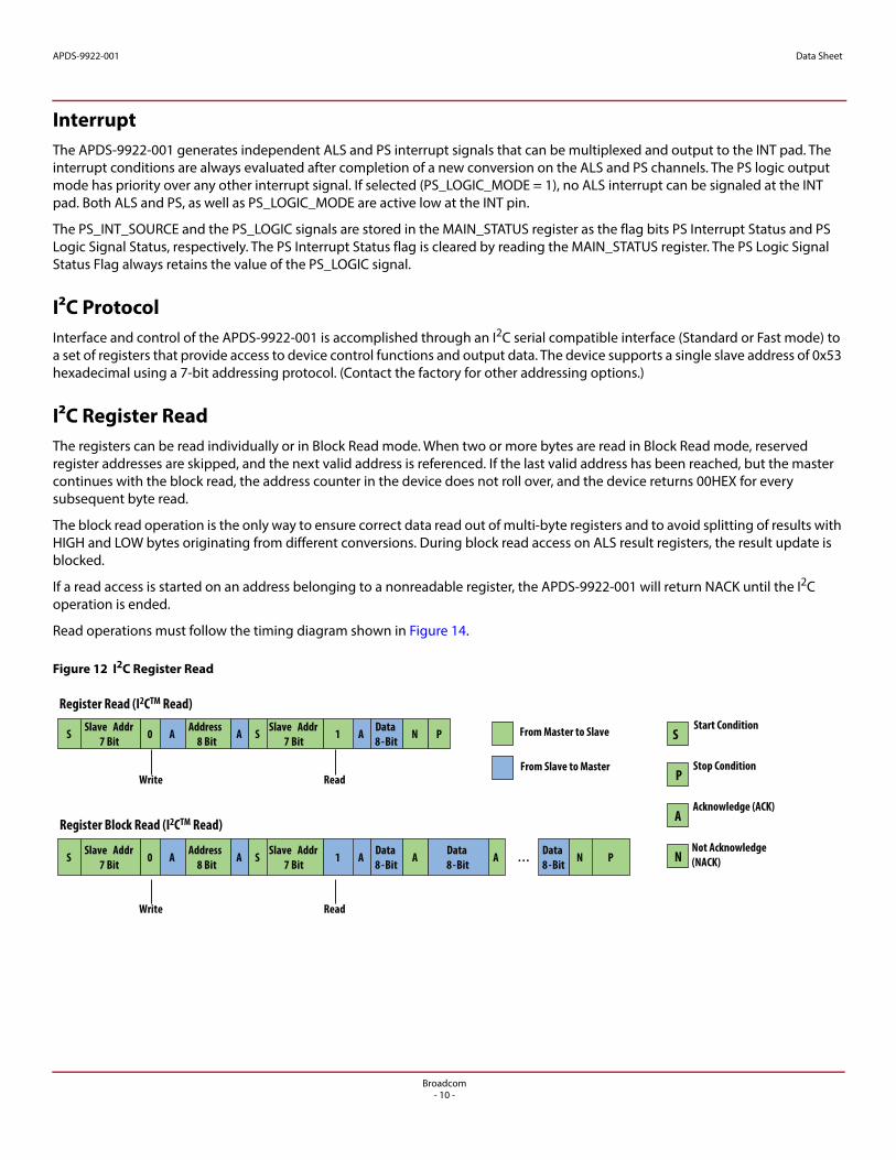
I2C Register WriteThe APDS-9922-001 registers can be written to individually or in Block Write mode. When two or more bytes are written in Block Write mode, reserved registers and read-only registers are skipped. The transmitted data is automatically applied to the next writable register. If a register includes read (R) and read/write (RW) bits, the register is not skipped. Data written to read-only bits are ignored.
If the last valid address of the APDS-9922-001 address range is reached but the master attempts to continue the block write operation, the address counter of the APDS-9922-001 does not roll over. The APDS-9922-001 returns NACK for every following byte sent by the master until the I2C operation is ended.
If a write access is started on an address belonging to a non-writeable register, the APDS-9922-001 returns NACK until the I2C operation is ended.
Write operations must follow the timing diagram shown in Figure 14.
Figure 13 I2C Register Write
S Slave Addr7 Bit 0 A Address A Data
8 -Bit A P
S Slave Addr7 Bit 0 A Address A Data
8 -Bit A Data 8 -Bit A … Data
8 -Bit A P
Write
Write
Register Write (I2CTM Write)
Register Block Write (I2CTM Write)
From Master to Slave
From Slave to Master
S
P
A
N
Start Condition
Stop Condition
Acknowledge (ACK)
Not Acknowledge (NACK)

Broadcom- 12 -
APDS-9922-001 Data Sheet
Figure 14 II2C Interface – Bus Timing
Table 10 Bus Timing Characteristics
Parameter Symbol Standard Mode Fast Mode Unit
Maximum SCL Clock Frequency fSCL 100 400 KHz
Minimum START Condition Hold Time Relative to SCL Edge tDSTA 4 — μs
Minimum SCL Clock Low Width tLOW 4.7 — μs
Minimum SCL Clock High Width tHIGH 4 — μs
Minimum START Condition Setup Time Relative to SCL Edge tSUSTA 4.7 — μs
Minimum Data Hold Time on SDA Relative to SCL Edge tHDDAT 0 — μs
Minimum Data Setup Time on SDA Relative to SCL Edge tSUDAT 0.1 0.1 μs
Minimum STOP Condition Setup Time on SCL tSUSTO 4 — μs
Minimum Bus Free Time Between Stop Condition and Start Condition tBUS 4.7 — μs
SDA
SCL
tLOW
tHDSTA
tBUStHDSTAtSUDAT
tSUSTOtSUSTA
tHIGHtHDDAT

Broadcom- 13 -
APDS-9922-001 Data Sheet
Register SetThe APDS-9922-001 is controlled and monitored by data registers and a command register accessed through the serial interface. These registers provide for a variety of control functions and can be read to determine results of the ADC conversions.
Table 11 Register Set
Address Type Name Description Reset Value
00HEX RW MAIN_CTRL ALS operation mode control, SW reset 00HEX
01HEX RW PS_LED PS LED settings 36HEX
02HEX RW PS_PULSES PS number of LED pulses 08HEX
03HEX RW PS_MEAS_RATE PS measurement rate in active mode 45HEX
04HEX RW ALS_MEAS_RATE ALS measurement rate and resolution in active mode 22HEX
05HEX RW ALS_GAIN ALS analog gain range 01HEX
06HEX R PART_ID Part number ID and revision ID B3HEX
07HEX R MAIN_STATUS Power-on status, interrupt status, data status 20HEX
08HEX R PS_DATA_0 PS measurement data, least significant bits 00HEX
09HEX R PS_DATA_1 PS measurement data, most significant bits, and overflow 00HEX
0DHEX R ALS_DATA_0 ALS ADC measurement data - LSB 00HEX
0EHEX R ALS_DATA_1 ALS ADC measurement data 00HEX
0FHEX R ALS_DATA_2 ALS ADC measurement data - MSB 00HEX
19HEX RW INT_CFG Interrupt configuration 10HEX
1AHEX RW INT_PERSISTENCE Interrupt persist setting 00HEX
1BHEX RW PS_THRES_UP_0 PS interrupt upper threshold, LSB FFHEX
1CHEX RW PS_THRES _UP_1 PS interrupt upper threshold, MSB 07HEX
1DHEX RW PS_THRES_LOW_0 PS interrupt lower threshold, LSB 00HEX
1EHEX RW PS_THRES_LOW_1 PS interrupt lower threshold, MSB 00HEX
1FHEX RW PS_CAN_0 PS intelligent cancellation level setting, LSB 00HEX
20HEX RW PS_CAN_1 PS intelligent cancellation level setting, MSB 00HEX
21HEX RW ALS_THRES_UP_0 ALS interrupt upper threshold, LSB FFHEX
22HEX RW ALS_THRES_UP_1 ALS interrupt upper threshold FFHEX
23HEX RW ALS_THRES_UP_2 ALS interrupt upper threshold, MSB 0FHEX
24HEX RW ALS_THRES_LOW_0 ALS interrupt lower threshold, LSB 00HEX
25HEX RW ALS_THRES_LOW_1 ALS interrupt lower threshold 00HEX
26HEX RW ALS_THRES_LOW_2 ALS interrupt lower threshold, MSB 00HEX
27HEX RW ALS_THRES_VAR ALS interrupt variance threshold 00HEX

Broadcom- 14 -
APDS-9922-001 Data Sheet
MAIN_CTRLDefault Value: 00HEX
Writing to this register stops the ongoing measurements (both ALS and PS) and starts new measurements (depending on the respective enable bits).
PS_LEDDefault Value: 36HEX
Writing to this register stops the ongoing measurements (both ALS and PS) and starts new measurements (depending on the respective enable bits).
7 6 5 4 3 2 1 0
0 0 0 SW_Reset 0 0 ALS_EN PS_EN 0X00
Field Bit Description
SW_Reset 4 1 = Reset will be triggered
ALS_EN 1 1 = ALS active0 = ALS standby
PS_EN 1 1 = PS active0 = PS standby
7 6 5 4 3 2 1 0
0 LED Pulse Modulation Frequency LED Current Peaking
LED Current 0X01
Field Bit Description
LED Pulse Modulation Frequency 6:4 000 = Reserved001= Reserved010 = Reserved011 = LED pulse frequency = 60 KHz (default)100 = LED pulse frequency = 70 KHz101 = LED pulse frequency = 80 KHz110 = LED pulse frequency = 90 KHz111 = LED pulse frequency = 100 KHz
LED Current Turn-On Acceleration (Peaking) On/Off
3 1 = LED current peaking on0 = LED current peaking off (default)
LED current 2:0 000 = LED pulsed current level = 2.5 mA001 = LED pulsed current level = 5.0 mA010 = LED pulsed current level = 10 mA011 = LED pulsed current level = 25 mA100 = LED pulsed current level = 50 mA101 = LED pulsed current level = 75 mA110 = LED pulsed current level = 100 mA (default)111 = LED pulsed current level = 125 mA

Broadcom- 15 -
APDS-9922-001 Data Sheet
PS_PULSESDefault Value: 08HEX
Writing to this register stops the ongoing measurements (both ALS and PS) and starts new measurements (depending on the respective enable bits).
PS_MEAS_RATEDefault Value: 45HEX
Bit 2:0 register controls the timing of the periodic measurements of the PS in Active Mode.
When the measurement repeat rate is programmed to be faster than possible for the programmed ADC measurement time, the repeat rate will be lower than programmed (maximum speed).
Writing to this register stops the ongoing measurements (both ALS and PS) and starts new measurements (depending on the respective enable bits).
7 6 5 4 3 2 1 0
PS Number of LED Pulses 0X02
Field Bit Description
PS_PULSES 7:0 00000000 = 0 pulses (no light emission)… ….00001000 = 8 pulses (default)… ….00100000 = 32 pulses
7 6 5 4 3 2 1 0
Reserved PS Resolution / Bit Width PS Measurement Rate 0X03
Field Bit Description
Reserved 7:5 Reserved. Write as 010.
PS Resolution 4:3 00 = 8 bit (default)01 = 9 bit10 = 10 bit11 = 11 bit
PS Measurement Rate 2:0 000 = Reserved001 = 6.25 ms010 = 12.5 ms011 = 25 ms100 = 50 ms101 = 100 ms (default)110 = 200 ms111 = 400 ms

Broadcom- 16 -
APDS-9922-001 Data Sheet
ALS_MEAS_RATEDefault Value: 22HEX
Bit 2:0 register controls the timing of the periodic measurements of the ALS in Active Mode.
When the measurement repeat rate is programmed to be faster than possible for the specified ADC measurement time, the repeat rate will be lower than programmed (maximum speed).
Writing to this register stops the ongoing measurement and starts new measurements (depending on the respective bits).
ALS_GAINDefault Value: 01HEX
Writing to this register stops the ongoing measurement and starts new measurements (depending on the respective bits).
7 6 5 4 3 2 1 0
0 ALS Resolution/Bit Width 0 ALS Measurement Rate 0X04
Field Bit Description
ALS Resolution/Bit Width 6:4 000 = 20 bit – 400 ms001 = 19 bit – 200 ms010 = 18 bit – 100 ms (default)011 = 17 bit – 50 ms100 = 16 bit – 25 ms101 = 13 bit – 3.125 ms110 = Reserved111 = Reserved
ALS Measurement Rate 2:0 000 = 25 ms001 = 50 ms010 = 100 ms (default)011 = 200 ms100 = 500 ms101 = 1000 ms110 = 2000 ms111 = 2000 ms
7 6 5 4 3 2 1 0
0 0 0 0 0 ALS Gain Range 0X05
Field Bit Description
ALS Gain Range 2:0 000 = Gain 1001 = Gain 3010 = Gain 6011 = Gain 9100 = Gain 18

Broadcom- 17 -
APDS-9922-001 Data Sheet
PART_IDDefault Value: B3HEX
MAIN_STATUSDefault Value: 20HEX
7 6 5 4 3 2 1 0
Part ID Revision ID 0X06
Field Bit Description
Part Number ID 7:4 Part number ID.
Revision ID 3:0 Revision ID of the component. The value increases by one each time a new silicon revision is manufactured.
7 6 5 4 3 2 1 0
0 0 Power On Status
ALS Interrupt Status
ALS Data Status
PS Logic Signal Status
PS Interrupt Status
PS DataStatus
0X07
Field Bit Description
Power On status 5 1 = Part went through a power-up event, either because the part was turned on or because there was power supply voltage disturbance. (default at first register read).All interrupt threshold settings in the registers have been reset to power-on default states and should be examined if necessary. The flag is cleared after the register is read.
ALS Interrupt status 4 0 = Interrupt condition not fulfilled (default).1 = Interrupt condition fulfilled (cleared after read).
ALS Data status 3 0 = Old data, already read (default).1 = New data, not yet read (cleared after read).
PS Logic Signal Status 2 0 = Object is far (default).1 = Object is close.
PS Interrupt Status 1 0 = Interrupt condition not fulfilled (default).1 = Interrupt condition fulfilled (cleared after read).
PS Data Status 0 0 = Old data, already read (default).1 = New data, not yet read (cleared after read).

Broadcom- 18 -
APDS-9922-001 Data Sheet
PS_DATADefault Value: 00HEX, 00HEX
If an I²C read operation is active and points to an address in the range 07HEX to 18HEX, both registers PS_DATA_0 and PS_DATA_1 are locked until the I²C read operation is completed or the specified address range is left.
This guarantees that the data in the registers comes from the same measurement even if an additional measurement cycle ends during the read operation. New measurement data is stored into temporary registers and the actual PS_DATA registers are updated as soon as there is no on-going I²C read operation to the address range 07HEX to 18HEX.
The PS conversion result is always written LSB-aligned into the PS_DATA registers, regardless of the conversion resolution selected in the PS_MEAS_RATE register. PS_DATA_1 is filled with 0 for resolutions lower than 11 bits.
If the PS data is outside of the measurable range, the Overflow flag (PS_DATA_1, Bit [3]) is set in any resolution mode.
PS_DATA is automatically corrected by the value of the PS cancellation register (PS_CAN).
PS_DATA = PS_meas – PS_CAN
PS_meas is the internal raw value obtained from the PS ADC. If PS_meas is already full-scale, the value of PS_DATA is set to its maximum value without subtracting the PS cancellation value.
ALS_DATADefault Value: 00HEX, 00HEX, 00HEX
ALS channel digital output data (unsigned integer, 13 to 20 bit, LSB aligned).
The ALS channel output is already compensated internally: ALS_DATA = (ALSint – COMP).
When an I²C read operation is active and points to an address in the range 07HEX to 18HEX, all registers in this range are locked until the I²C read operation is completed or this address range is left.
This guarantees that the data in the registers comes from the same measurement even if an additional measurement cycle ends during the read operation. New measurement data is stored into temporary registers and the actual ALS_DATA registers are updated as soon as there is no ongoing I²C read operation to the address range 07HEX to 18HEX.
7 6 5 4 3 2 1 0
PS_DATA_0 0X08
0 0 0 0 Overflow PS_DATA_1 0x09
Reg 08HEX Bit[7:0] PS measurement least significant data byte, bit 0 is the LSB of the data word
Reg 09HEX Bit[2:0] PS measurement most significant data byte, bit 2 is MSB in 11-bit mode
Bit[3] 0: valid PS data (default); 1: overflow of PS data
7 6 5 4 3 2 1 0
ALS_DATA_0 [7:0] 0X0D
ALS_DATA _1 [15:8] 0X0E
0 0 0 0 ALS_DATA_2 [19:16] 0X0F
Reg 0DHEX Bit[7:0] ALS diode data least significant data byte
Reg 0EHEX Bit[7:0] ALS diode data intervening data byte
Reg 0FHEX Bit[3:0] ALS diode data most significant data byte

Broadcom- 19 -
APDS-9922-001 Data Sheet
INT_CFGDefault Value: 10HEX
INT_PERSISTENCEDefault Value: 00HEX
This register sets the number of similar consecutive LS interrupt events that must occur before the interrupt is asserted.
7 6 [5:4] 3 2 1 0
0 0 ALS_Interrupt Source
ALS VariationInterrupt Mode
ALS InterruptEnable
PS LogicOutput
PS InterruptEnable
0X19
0 0 ALS_INT_SEL ALS_VAR_MODE ALS_INT_EN PS_LOGIC_MODE
PS_INT_EN
Field Bit Description
ALS_INT_SEL 5:4 00 = Clear channel.01 = ALS channel (default).
ALS_VAR_MODE 3 0 = ALS threshold interrupt mode (default).1 = ALS variation interrupt mode.
ALS_INT_EN 2 0 = ALS Interrupt disabled (default).1 = ALS Interrupt enabled.
PS_LOGIC_MODE 1 0 = Normal interrupt function: after interrupt event, INT pad maintains active level until MAIN_STATUS register is read (default).1 = PS Logic Output Mode: INT pad is updated after every measurement and maintains output state between measurements.
PS_INT_EN 0 0 = PS Interrupt disabled (default).1 = PS Interrupt enabled.
7 6 5 4 3 2 1 0
ALS_PERSIST PS_PERSIST 0X1A
Field Bit Description
ALS_PERSIST 7:4 0000 = Every ALS value out of threshold range (default) asserts an interrupt.0001 = 2 consecutive ALS values out of threshold range assert an interrupt.…1111 = 16 consecutive ALS values out of threshold range assert an interrupt.
PS_PERSIST 3:0 0000 = Every PS value out of threshold range (default) asserts an interrupt.0001 = 2 consecutive PS values out of threshold range assert an interrupt.…1111 = 16 consecutive PS values out of threshold range assert an interrupt.

Broadcom- 20 -
APDS-9922-001 Data Sheet
PS_THRESH_UPDefault Value: FFHEX, 07HEX
PS_THRES_UP_x sets the upper threshold value for the PS interrupt. The Interrupt Controller compares the value in PS_THRES_UP_x against measured data in the PS_DATA_x registers. It generates an interrupt event if PS_DATA_x exceeds the upper threshold level.
The data format for PS_THRES_UP_x must match that of the PS_DATA_x registers.
For resolutions below 11 bits, the threshold is evaluated LSB-aligned.
PS_THRESH_LOWDefault Value: 00HEX, 00HEX
PS_THRES_LOW_x sets the lower threshold value for the PS interrupt. The Interrupt Controller compares the value in PS_THRES_LOW_x against measured data in the PS_DATA_x registers. It generates an interrupt event if PS_DATA_x is lower than the lower threshold level.
For resolutions below 11 bit, the threshold is evaluated LSB-aligned.
PS_INTELLIGENT CANCELLATION LEVELDefault Value: 00HEX, 00HEX
The PS cancellation level is expected to be written by the MCU during system start up. The value is subtracted from the measured PS data before the data is transferred to the PS_Data registers and evaluated by the Interrupt Controller.
7 6 5 4 3 2 1 0
PS_THRES_UP_0 0X1B
0 0 0 0 0 PS_THRES_UP_1 0X1C
Reg 1BHEX Bit[7:0] PS upper interrupt threshold value, LSB
Reg 1CHEX Bit[2:0] PS upper interrupt threshold value, intervening byte
7 6 5 4 3 2 1 0
PS_THRES_LOW_0 0x1D
0 0 0 0 0 PS_THRES_LOW_1 0x1E
Reg 1DHEX Bit[7:0] PS lower interrupt threshold value, LSB
Reg 1EHEX Bit[2:0] PS lower interrupt threshold value, intervening byte
7 6 5 4 3 2 1 0
PS_CAN _0 0X1F
0 0 0 0 0 PS_CAN_1 0x20
Reg 1FHEX Bit[7:0] PS cancellation level, LSB
Reg 20HEX Bit[2:0] PS cancellation level, MSB

Broadcom- 21 -
APDS-9922-001 Data Sheet
ALS_THRESH_UPDefault Value: FFHEX, FFHEX, 0FHEX
ALS_THRES_UP_x sets the upper threshold value for the ALS interrupt. The Interrupt Controller compares the value in ALS_THRES_UP_x against measured data in the ALS_DATA_x registers of the selected ALS interrupt channel. It generates an interrupt event if ALS_DATA_x exceeds the threshold level.
The data format for ALS_THRES_UP_x must match that of the ALS_DATA_x registers.
ALS_THRESH_LOWDefault Value: 00HEX, 00HEX, 00HEX
ALS_THRES_LOW_x sets the lower threshold value for the ALS interrupt. The Interrupt Controller compares the value in ALS_THRES_LOW_x against measured data in the ALS_DATA_x registers of the selected LS interrupt channel. It generates an interrupt event if the ALS_DATA_x is below the threshold level.
The data format for ALS_THRES_LOW_x must match that of the ALS_DATA_x registers.
7 6 5 4 3 2 1 0
ALS_THRES_UP_0 0X21
ALS_THRES_UP_1 0x22
0 0 0 0 ALS_THRES_UP_2 0x23
Reg 21HEX Bit[7:0] ALS upper interrupt threshold value, LSB
Reg 22HEX Bit[7:0] ALS upper interrupt threshold value, intervening byte
Reg 23HEX Bit[3:0] ALS upper interrupt threshold value, MSB
7 6 5 4 3 2 1 0
ALS_THRES_LOW_0 0X24
ALS_THRES_LOW_1 0x25
0 0 0 0 ALS_THRES_LOW_2 0x26
Reg 24HEX Bit[7:0] ALS lower interrupt threshold value, LSB
Reg 25HEX Bit[7:0] ALS lower interrupt threshold value, intervening byte
Reg 26HEX Bit[3:0] ALS lower interrupt threshold value, MSB

Broadcom- 22 -
APDS-9922-001 Data Sheet
ALS_THRESH_VARDefault Value: 00HEX
7 6 5 4 3 2 1 0
0 0 0 0 0 ALS_THRES_VAR 0X27
Field Bit Description
ALS_THRES_VAR 2:0 000 = ALS result varies by 8 counts compared to previous result001 = ALS result varies by 16 counts compared to previous result010 = ALS result varies by 32 counts compared to previous result011 = ALS result varies by 64 counts compared to previous result…111 = ALS result varies by 1024 counts compared to previous result

Broadcom- 23 -
APDS-9922-001 Data Sheet
Application Information: HardwareIn a proximity sensing system, the included IR LED can be pulsed with more than 100 mA of rapidly switching current, therefore, a few design considerations must be kept in mind to get the best performance. The key goal is to reduce the power supply noise coupled back into the device during the LED pulses. Averaging of multiple proximity samples is recommended to reduce the proximity noise.
The first recommendation is to use two power supplies; one for the device VDD and the other for the IR LED. In many systems, there is a quiet analog supply and a noisy digital supply. By connecting the quiet supply to the VDD pin and the noisy supply to the LEDA pin, the key goal can be met. Place a 1-μF low-ESR decoupling capacitor as close as possible to the VDD pin and 4.7 μF at the LEDA pin, and at least 10 μF of bulk capacitance to supply the 100 mA current surge.
Figure 15 Proximity Sensing using Separate Power Supplies
If it is not possible to provide two separate power supplies, the device can be operated from a single supply. A 100Ω resistor in series with the VDD supply line and a 4.7-μF ESR capacitor effectively filter any power supply noise. The previous capacitor placement considerations apply.
Figure 16 Proximity Sensing using a Single Power Supply
VBUS in the preceding figures refers to the I2C bus voltage. The I2C signals and the Interrupt are open-drain outputs and require pull-up resistors. The pull-up resistor (RP) value is a function of the I2C bus speed, the I2C bus voltage, and the capacitive load. A 10-kΩ pull-up resistor (RPI) can be used for the interrupt line.
APDS-9922-001 INT
SDA
SCL
V DD
LEDA
1 F
VoltageRegulator
VoltageRegulator
10 F
* Cap Value Per Regulator Manufacturer Recommendation
GND
V BUS
R P R P R PIC*
4.7 F
LDR
LEDK
4.7 F
VoltageRegulator
22 F
4.7 F
100
APDS-9922-001 INT
SDA
SCL
V DD
LEDA
GND
V BUS
R P R P R PILDR
LEDK

Broadcom- 24 -
APDS-9922-001 Data Sheet
Figure 17 Package Outline Dimensions
NOTE All linear dimensions are in mm.
Suggested PCB pad layout guidelines for the Dual Flat No-Lead surface mount package are as follows.
Figure 18 PCB Pad Layout
NOTE All linear dimensions are in mm.
1
2
3
44
3
2
1
PINOUT1 - SDA2 - INT3 - LDR4 - LEDK5 - LEDA6 - GND7 - SCL8 - VDD
5
6
7
8
5
6
7
8
CL
CL
0.32 ±0.075
(0.30)
Ø 1.10 ±0.075
1.45 ±0.075
R0.20 ±0.075(0
.84)
0.60 ±0.10
PD
LED
CLHole Centre toShield CL ±0.10
2.10 ±0.10
2.36 ±0.20
1.35
±0.
10
3.73
±0.
10
3.94
±0.
20
0.51 ±0.10(x4)
0.70 ±0.10 (x8)
1.40 ±0.10 (x4)
1.52 ±0.10(x4)
0.60 ±0.075(x8)
0.60 ±0.075(x8)
CL
0.75 (x4)0.75 (x4)
0.11 0.11
0.26
(x6)
0.65
0.75
(x8)
Keep OutArea

Broadcom- 25 -
APDS-9922-001 Data Sheet
Figure 19 Tape Dimensions
Figure 20 Reel Dimensions
12
+ -0.30
0.10
4 ±0.10
2 ±0.05
4 ±0.10
1.7
5 ±
0.10
5.5
0 ±
0.05
1 ±0.05
1.50 ±0.10
B
B A AUnitOrientation
0.30 ±0.05
4.3
0 ±
0.10
1.70 ±0.10
SECTION B-BSCALE 4 : 1
6 Max Ref
2.70 ±0.10
SECTION A-A8 Max Ref
K0
A 0
B0
Tape Direction
Ø 20.200 min.
T
Ø 33
0 max
.
1.500 min.TapeStartSlot
Access Hole
Arbor Hole
Hub Dia.
Measuredat Hub
Measured atOuter Edge
13 ±0.200
W1
W3
100 ±0.500
W2
Measuredat Hub
TTAPE WIDTH W1 W2 W34± .5012MM 12.4 + 2.0
- 0.018.4 MAX 11.9 MIN.
15.4 MAX.

Broadcom- 26 -
APDS-9922-001 Data Sheet
Moisture Proof PackagingAll APDS-9922-001 options are shipped in moisture proof package. Once opened, moisture absorption begins. This part is compliant to JEDEC MSL 3.
Figure 21 Moisture Proof Packaging
If the parts are not stored in dry conditions, they must be baked before reflow to prevent damage to the parts.
Baking should only be done once.
Time from unsealing to soldering:
After removal from the bag, the parts should be soldered within 168 hours if stored at the recommended storage conditions. If times longer than 168 hours are needed, the parts must be stored in a dry box.
Units in A SealedMositure-Proof
Package
Package IsOpened (Unsealed)
Environmentless than 30 deg C, and
less than 60% RH?
Package IsOpened less
than 168 hours?
Perform RecommendedBaking Conditions
No BakingIs Necessary
No
Yes
No
Yes
Table 12 Backing Conditions
Package Temperature Time
In Reel 60°C 48 hours
In Bulk 100°C 4 hours
Table 13 Recommended Storage Conditions
Storage Temperature 10°C to 30°C
Relative Humidity below 60% RH

Broadcom- 27 -
APDS-9922-001 Data Sheet
Figure 22 Recommended Reflow Profile
The reflow profile is a straight-line representation of a nominal temperature profile for a convective reflow solder process. The temperature profile is divided into four process zones, each with different ∆T/∆time temperature change rates or duration. The T/time rates or duration are detailed in the above table. The temperatures are measured at the component to printed circuit board connections.
In process zone P1, the PC board and component pins are heated to a temperature of 150°C to activate the flux in the solder paste. The temperature ramp up rate, R1, is limited to 3°C per second to allow for even heating of both the PC board and component pins.
Process zone P2 should be of sufficient time duration (100s to 180s) to dry the solder paste. The temperature is raised to a level just below the liquidus point of the solder.
Process zone P3 is the solder reflow zone. In zone P3, the temperature is quickly raised above the liquidus point of solder to 260°C (500°F) for optimum results. The dwell time above the liquidus point of solder should be between 60s and 120s. This is to assure proper coalescing of the solder paste into liquid solder and the formation of good solder connections. Beyond the recommended dwell time the intermetallic growth within the solder connections becomes excessive, resulting in the formation of weak and unreliable connections. The temperature is then rapidly reduced to a point below the solidus temperature of the solder to allow the solder within the connections to freeze solid.
Process zone P4 is the cool down after solder freeze. The cool down rate, R5, from the liquidus point of the solder to 25°C (77°F) should not exceed 6°C per second maximum. This limitation is necessary to allow the PC board and component pins to change dimensions evenly, putting minimal stresses on the component.
It is recommended to perform reflow soldering no more than twice.
Table 14 Process Zones
Process Zone Symbol ΔT Maximum ΔT/Δtimeor Duration
Heat Up P1, R1 25°C to 150°C 3°C/s
Solder Paste Dry P2, R2 150°C to 200°C 100s to 180s
Solder Reflow P3, R3P3, R4
200°C to 260°C260°C to 200°C
3°C/s–6°C/s
Cool Down P4, R5 200°C to 25°C –6°C/s
Time maintained above liquidus point, 217 °C > 217°C 60s to 120s
Peak Temperature 260°C —
Time within 5 °C of actual Peak Temperature > 255°C 20s to 40s
Time 25 °C to Peak Temperature 25°C to 260°C 8 mins
50 100 150 200 250 300
t-TIME(SECONDS)
25
80
120150180200
230
255
0
TEM
PERA
TURE
(°C)
R1
R2
R3 R4
R5
217
MAX 260° C
P1HEAT UP
P2SOLDER PASTE DRY
P3SOLDERREFLOW
P4COOL DOWN
60 sec to 120 secAbove 217° C

For product information and a complete list of distributors, please go to our web site: www.broadcom.com.
Broadcom, the pulse logo, Connecting everything, Avago Technologies, Avago, and the A logo are among the trademarks of Broadcom in the United States, certain other countries and/or the EU.
Copyright © 2016–2018 Broadcom. All Rights Reserved.
The term "Broadcom" refers to Broadcom Inc. and/or its subsidiaries. For more information, please visit www.broadcom.com.
Broadcom reserves the right to make changes without further notice to any products or data herein to improve reliability, function, or design.
Information furnished by Broadcom is believed to be accurate and reliable. However, Broadcom does not assume any liability arising out of the application or use of this information, nor the application or use of any product or circuit described herein, neither does it convey any license under its patent rights nor the rights of others.
APDS-9922-001-DS102 – August 29, 2018


![[MS-APDS]: Authentication Protocol Domain Support · Security (TLS), and Digest authentication. APDS is used by NT LAN Manager (NTLM) and the APDS is used by NT LAN Manager (NTLM)](https://img.dokumen.tips/doc/110x75/5fe60c7971901a24cb29f5b7/ms-apds-authentication-protocol-domain-support-security-tls-and-digest-authentication.jpg)