Embed Size (px)
Citation preview

AP7167
1.2A LOW DROPOUT REGULATOR WITH POK
AP7167 Document number: DS31252 Rev. 7 - 2
1 of 14 www.diodes.com
September 2010 © Diodes Incorporated
Description
The AP7167 is a 1.2A, adjustable output voltage, ultra-low dropout linear regulator. The device includes pass element, error amplifier, band-gap reference, current limit and thermal shutdown circuitry. The device is turned on when EN pin is set to logic high level. A Power-OK (POK) output is available for power sequence control. The characteristics of the low dropout voltage and low quiescent current make it suitable for low to medium power applications, for example, laptop computers, audio and video applications, and battery powered devices. The typical quiescent current is approximately 125µA. Built-in current-limit and thermal-shutdown functions prevent IC from damage in fault conditions. The AP7167 are available in DFN3030-10 and SOP-8L packages.
Features • Wide input voltage range: 2.2V – 5.5V • 230mV very low dropout at 500mA load • 500mV very low dropout at 1A load • 3% total accuracy over line, load and temperature • Very low quiescent current (IQ): 125µA typical • Adjustable output voltage range: 0.8V to 5.0V • Very fast transient response • High PSRR • Accurate voltage regulation • Current limiting and short circuit protection • Thermal shutdown protection • Stable with any type output capacitor ≥ 4.7µF • Ambient temperature range -40ºC to 85 ºC • DFN3030-10 and SOP-8L-EP: Available in “Green”
Molding Compound (No Br, Sb) • Lead Free Finish/ RoHS Compliant (Note 1)
Pin Assignments
( Top View )
FB
EN
IN
GND
OUT
POK
1
2
5
NC
IN
3
4
6
8
7
10
9
NC
OUT
DFN3030-10
FBPOK
EN
IN
OUT
GND
OUT
( Top View )
1
2
3
4
8
7
6
5
IN
SOP-8L-EP
Applications
• Servers and laptops • Smart phone and PDA • MP3/MP4 • Bluetooth headset • Low and medium power applications • FPGA and DSP core or I/O power
Notes: 1. EU Directive 2002/95/EC (RoHS). All applicable RoHS exemptions applied. Please visit our website at
http://www.diodes.com/products/lead_free.html.
AP7167
1.2A LOW DROPOUT REGULATOR WITH POK
AP7167 Document number: DS31252 Rev. 7 - 2
2 of 14 www.diodes.com
September 2010 © Diodes Incorporated
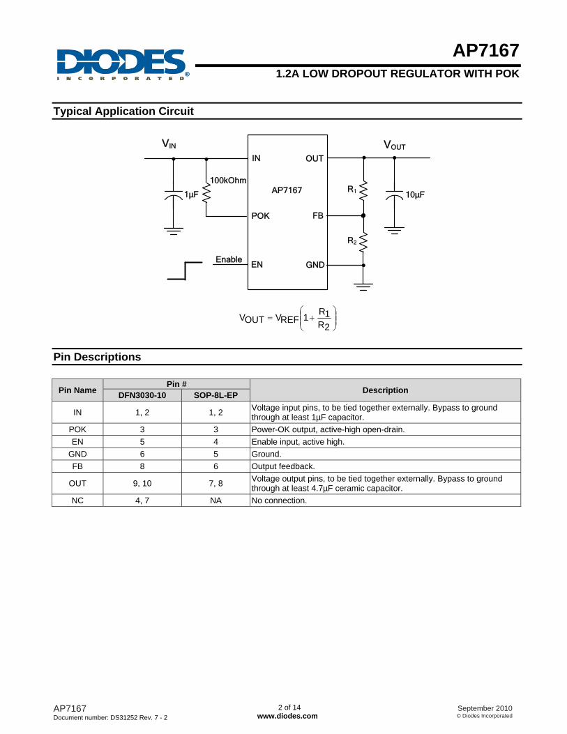
Typical Application Circuit
1µF
IN
GNDEN
OUT
Enable
FB
10µF
VIN VOUT
POK
100kOhmR1
R2
AP7167
⎟⎟⎠
⎞⎜⎜⎝
⎛+=
2R1R1REFVOUTV
Pin Descriptions
Pin Name Pin #
Description DFN3030-10 SOP-8L-EP
IN 1, 2 1, 2 Voltage input pins, to be tied together externally. Bypass to ground through at least 1µF capacitor.
POK 3 3 Power-OK output, active-high open-drain. EN 5 4 Enable input, active high.
GND 6 5 Ground. FB 8 6 Output feedback.
OUT 9, 10 7, 8 Voltage output pins, to be tied together externally. Bypass to ground through at least 4.7µF ceramic capacitor.
NC 4, 7 NA No connection.

AP7167
1.2A LOW DROPOUT REGULATOR WITH POK
AP7167 Document number: DS31252 Rev. 7 - 2
3 of 14 www.diodes.com
September 2010 © Diodes Incorporated
Functional Block Diagram
IN
EN
GND
FB
OUT
Gate Driver
0.8V
0.744V
POK
Current Limit and Thermal
Shutdown
Absolute Maximum Ratings
Symbol Parameter Ratings Unit ESD HBM Human Body Model ESD Protection 4 KV ESD MM Machine Model ESD Protection 300 V
VIN Input Voltage 7 V OUT, FB, POK, EN Voltage VIN + 0.3 V Continuous Load Current Internal Limited
TJ Operating Junction Temperature Range -40 ~ 150 °C
TST Storage Temperature Range -65 ~150 °C
PD Power Dissipation DFN3030-10 (Note 2, 4) 3.1 W SOP-8L-EP (Note 2, 5) 4.0 W
Notes: 2. Ratings apply to ambient temperature at 25°C
Recommended Operating Conditions
Symbol Parameter Min Max Unit
VIN Input voltage 2.2 5.5 V
IOUT Output Current 0 1.2 A
TA Operating Ambient Temperature -40 85 °C
AP7167
1.2A LOW DROPOUT REGULATOR WITH POK
AP7167 Document number: DS31252 Rev. 7 - 2
4 of 14 www.diodes.com
September 2010 © Diodes Incorporated
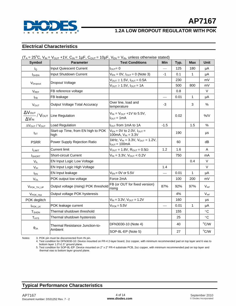
Electrical Characteristics (TA = 25oC, VIN
= VOUT +1V, CIN = 1µF, COUT
= 10µF, VEN = VIN, unless otherwise stated)
Symbol Parameter Test Conditions Min Typ. Max Unit
IQ Input Quiescent Current IOUT= 0 ⎯ 125 180 µA
ISHDN Input Shutdown Current VEN = 0V, IOUT = 0 (Note 3) -1 0.1 1 µA
VDropout Dropout Voltage VOUT ≥ 1.5V, IOUT = 0.5A 230 mV VOUT ≥ 1.5V, IOUT = 1A 500 800 mV
VREF FB reference voltage 0.8 V
IFB FB leakage ⎯ 0.01 1 µA
VOUT Output Voltage Total Accuracy Over line, load and temperature -3 3 %
OUTIN
OUT VΔVΔV / Line Regulation VIN = VOUT +1V to 5.5V,
IOUT = 1mA 0.02 %/V
ΔVOUT / VOUT Load Regulation IOUT from 1mA to 1A -1.5 1.5 %
tST Start-up Time, from EN high to POK high
VEN = 0V to 2.0V, IOUT = 100mA, VIN = 3.3V 190 µs
PSRR Power Supply Rejection Ratio 1kHz, VIN = 3.3V, VOUT = 1.2V, IOUT = 100mA 60 dB
ILIMIT Current limit VOUT = 1.8V, ROUT = 0.5Ω 1.2 1.6 A
ISHORT Short-circuit Current VIN = 3.3V, VOUT < 0.2V 750 mA
VIL EN Input Logic Low Voltage 0.4 V
VIH EN Input Logic High Voltage 1.4 V
IEN EN Input leakage VEN = 0V or 5.5V ⎯ 0.01 1 µA
VOL POK output low voltage Force 2mA 100 200 mV
VPOK_TH_UP Output voltage (rising) POK threshold FB (or OUT for fixed version) rising 87% 92% 97% Vref
VPOK_Hys Output voltage POK hysteresis 4% Vref
POK deglitch VIN = 3.3V, VOUT = 1.2V 160 µs
IPOK_LK POK leakage current VPOK = 5.5V ⎯ 0.01 1 µA
TSHDN Thermal shutdown threshold 155 °C
THYS Thermal shutdown hysteresis 25 °C
θJA Thermal Resistance Junction-to-Ambient
DFN3030-10 (Note 4) 40 oC/W
SOP-8L-EP (Note 5) 27 oC/W
Notes: 3. POK pin must be disconnected from IN pin. 4. Test condition for DFN3030-10: Device mounted on FR-4 2-layer board, 2oz copper, with minimum recommended pad on top layer and 6 vias to bottom layer 1.0”x1.5” ground plane. 5. Test condition for SOP-8L-EP: Device mounted on 2" x 2" FR-4 substrate PCB, 2oz copper, with minimum recommended pad on top layer and thermal vias to bottom layer ground plane.
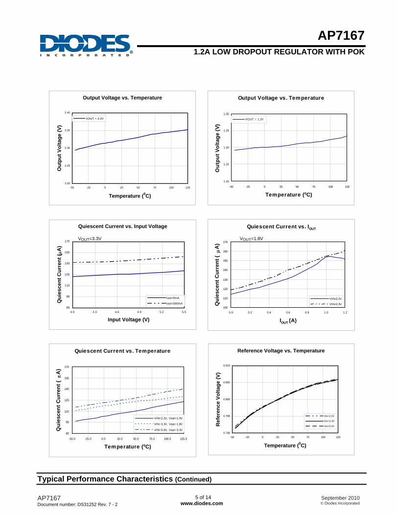
Typical Performance Characteristics
AP7167
1.2A LOW DROPOUT REGULATOR WITH POK
AP7167 Document number: DS31252 Rev. 7 - 2
5 of 14 www.diodes.com
September 2010 © Diodes Incorporated
Output Voltage vs. Temperature
3.20
3.25
3.30
3.35
3.40
-50 -25 0 25 50 75 100 125
Temperature (0C)
Out
put V
olta
ge (V
)
VOUT = 3.3V
Output Voltage vs. Temperature
1.10
1.15
1.20
1.25
1.30
-50 -25 0 25 50 75 100 125
Temperature (0C)
Out
put V
olta
ge (V
)
VOUT = 1.2V
Quiescent Current vs. Input Voltage
80
95
110
125
140
155
170
4.0 4.3 4.6 4.9 5.2 5.5
Input Voltage (V)
Qui
esce
nt C
urre
nt ( μ
A)
Iout=0mA
Iout=500mA
Quiescent Current vs. IOUT
100
110
120
130
140
150
160
170
0.0 0.2 0.4 0.6 0.8 1.0 1.2
IOUT (A)
Qui
esce
nt C
urre
nt (
μA
)
VIN=2.5V
VIN=3.3V
Quiescent Current vs. Temperature
80
95
110
125
140
155
170
-50.0 -25.0 0.0 25.0 50.0 75.0 100.0 125.0
Temperature (0C)
Qui
esce
nt C
urre
nt (π
A)
VIN=2.2V, Vout=1.0V
VIN=3.3V, Vout=1.8V
VIN=5.0V, Vout=3.3V
Reference Voltage vs. Temperature
0.790
0.795
0.800
0.805
0.810
-50 -25 0 25 50 75 100 125
Temperature (0C)
Ref
eren
ce V
olta
ge (V
)
Vin=2.2V
Vin=3.3V
Vin=5.5V
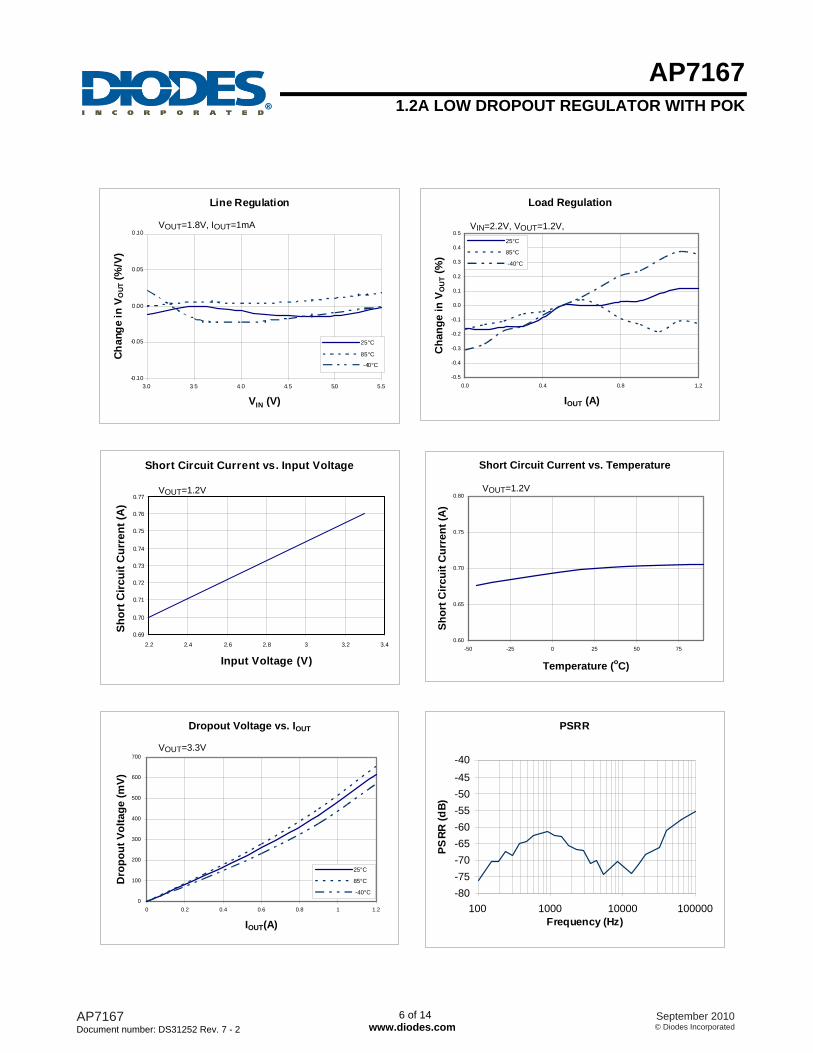
Typical Performance Characteristics (Continued)
VOUT=1.8V VOUT=3.3V
AP7167
1.2A LOW DROPOUT REGULATOR WITH POK
AP7167 Document number: DS31252 Rev. 7 - 2
6 of 14 www.diodes.com
September 2010 © Diodes Incorporated
Line Regulation
-0.10
-0.05
0.00
0.05
0.10
3.0 3.5 4.0 4.5 5.0 5.5
VIN (V)
Chan
ge in
VO
UT (%
/V)
25°C
85°C
-40°C
Load Regulation
-0.5
-0.4
-0.3
-0.2
-0.1
0.0
0.1
0.2
0.3
0.4
0.5
0.0 0.4 0.8 1.2
IOUT (A)
Cha
nge
in V
OU
T (%
)
25°C
85°C
-40°C
Short Circuit Current vs. Input Voltage
0.69
0.70
0.71
0.72
0.73
0.74
0.75
0.76
0.77
2.2 2.4 2.6 2.8 3 3.2 3.4
Input Voltage (V)
Shor
t Circ
uit C
urre
nt (A
)
Short Circuit Current vs. Temperature
0.60
0.65
0.70
0.75
0.80
-50 -25 0 25 50 75
Temperature (oC)
Shor
t Circ
uit C
urre
nt (A
)
Dropout Voltage vs. IOUT
0
100
200
300
400
500
600
700
0 0.2 0.4 0.6 0.8 1 1.2
IOUT(A)
Dro
pout
Vol
tage
(mV)
25°C
85°C
-40°C
PSRR
-80-75-70-65-60-55-50-45
-40
100 1000 10000 100000Frequency (Hz)
PSRR
(dB)
VOUT=1.8V, IOUT=1mA VIN=2.2V, VOUT=1.2V,
VOUT=1.2V VOUT=1.2V
VOUT=3.3V

AP7167
1.2A LOW DROPOUT REGULATOR WITH POK
AP7167 Document number: DS31252 Rev. 7 - 2
7 of 14 www.diodes.com
September 2010 © Diodes Incorporated
Typical Performance Characteristics (Continued)
Line Transient Response
Time (5ms/div)
Line Transient Response
Time (500us/div)
Output Load Transient Response (VOUT=1.8V)
Time (100us/div)
Output Load Transient Response (VOUT=3.3V)
Time (100us/div)
Start-up Time (VOUT=1.2V, IOUT=0.1A)
Time (50us/div)
Start-up Time (VOUT=1.2V, IOUT=1.2A)
Time (50us/div)
VIN 2V/div
VOUT 50mV/div
VIN =3V to 5.5V
COUT =10uF (Ceramic) IOUT =200mA
COUT=470uF (electrolytic)
100mV/div
500mA/div
50mA
1.2A
1A/us
COUT=10uF (Ceramic)
COUT=1uF (Ceramic)
VOUT
IOUT
VIN 2V/div
VOUT 50mV/div
VIN =5.5V to 3V
COUT =10uF (Ceramic) IOUT =200mA
COUT=470uF (electrolytic)
100mV/div
500mA/div
50mA
1.2A
1A/us
COUT=10uF (Ceramic)
COUT=1uF (Ceramic)
VOUT
IOUT
VEN 2V/div
VOUT 1V/div
VPOK 2V/div
COUT=10uF
VEN 2V/div
VOUT 1V/div
VPOK 2V/div
COUT=10uF
AP7167
1.2A LOW DROPOUT REGULATOR WITH POK
AP7167 Document number: DS31252 Rev. 7 - 2
8 of 14 www.diodes.com
September 2010 © Diodes Incorporated
Typical Performance Characteristics (Continued)
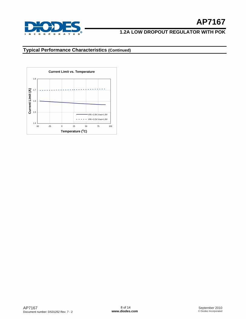
Current Limit vs. Temperature
1.4
1.5
1.6
1.7
1.8
-50 -25 0 25 50 75 100
Temperature (oC)
Cur
rent
Lim
it (A
)
VIN =2.8V,Vout=1.8V
VIN =3.3V,Vout=1.8V
AP7167
1.2A LOW DROPOUT REGULATOR WITH POK
AP7167 Document number: DS31252 Rev. 7 - 2
9 of 14 www.diodes.com
September 2010 © Diodes Incorporated
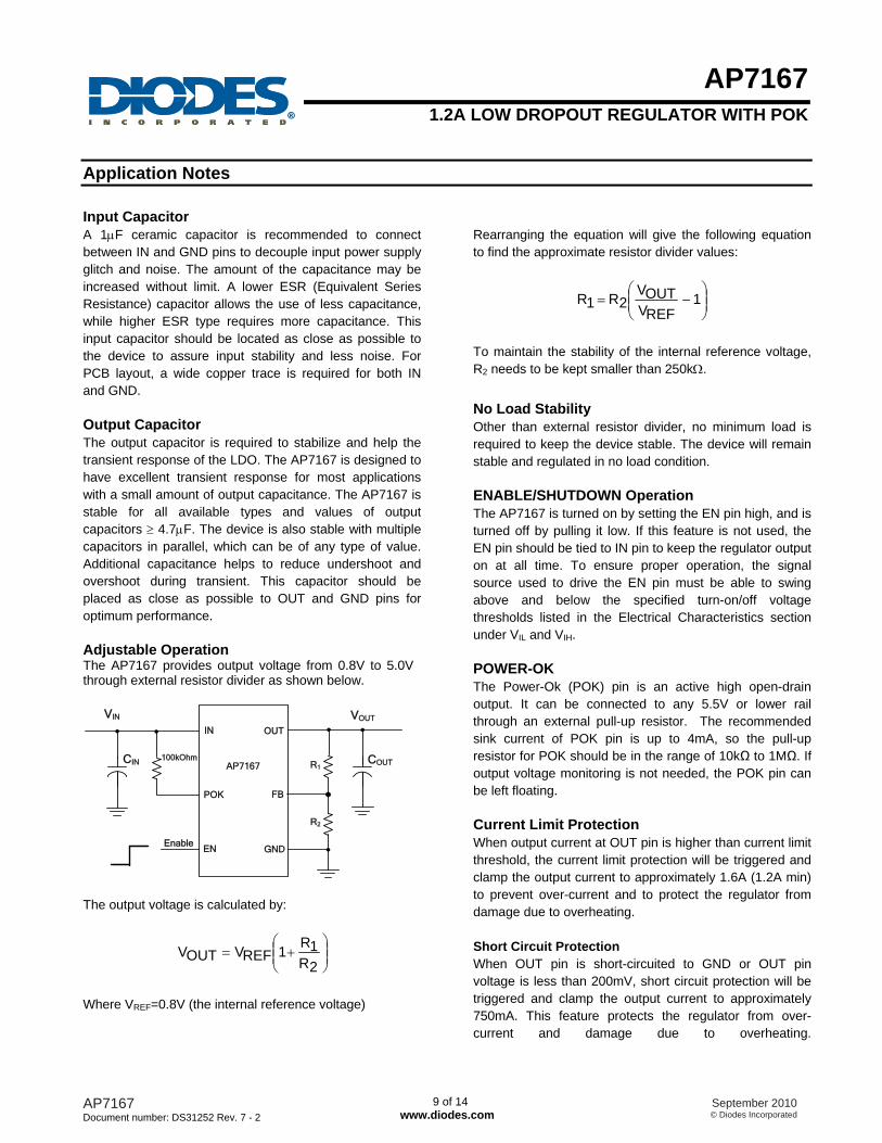
Application Notes Input Capacitor A 1μF ceramic capacitor is recommended to connect between IN and GND pins to decouple input power supply glitch and noise. The amount of the capacitance may be increased without limit. A lower ESR (Equivalent Series Resistance) capacitor allows the use of less capacitance, while higher ESR type requires more capacitance. This input capacitor should be located as close as possible to the device to assure input stability and less noise. For PCB layout, a wide copper trace is required for both IN and GND. Output Capacitor The output capacitor is required to stabilize and help the transient response of the LDO. The AP7167 is designed to have excellent transient response for most applications with a small amount of output capacitance. The AP7167 is stable for all available types and values of output capacitors ≥ 4.7μF. The device is also stable with multiple capacitors in parallel, which can be of any type of value. Additional capacitance helps to reduce undershoot and overshoot during transient. This capacitor should be placed as close as possible to OUT and GND pins for optimum performance. Adjustable Operation The AP7167 provides output voltage from 0.8V to 5.0V through external resistor divider as shown below.
IN
GNDEN
OUT
Enable
FB
VIN VOUT
POK
100kOhmR1
R2
AP7167CIN COUT
The output voltage is calculated by:
⎟⎟⎠
⎞⎜⎜⎝
⎛+=
2R1R1REFVOUTV
Where VREF=0.8V (the internal reference voltage)
Rearranging the equation will give the following equation to find the approximate resistor divider values:
⎟⎟⎠
⎞⎜⎜⎝
⎛−= 1
REFVOUTV
2R1R
To maintain the stability of the internal reference voltage, R2 needs to be kept smaller than 250kΩ.
No Load Stability Other than external resistor divider, no minimum load is required to keep the device stable. The device will remain stable and regulated in no load condition. ENABLE/SHUTDOWN Operation The AP7167 is turned on by setting the EN pin high, and is turned off by pulling it low. If this feature is not used, the EN pin should be tied to IN pin to keep the regulator output on at all time. To ensure proper operation, the signal source used to drive the EN pin must be able to swing above and below the specified turn-on/off voltage thresholds listed in the Electrical Characteristics section under VIL and VIH. POWER-OK The Power-Ok (POK) pin is an active high open-drain output. It can be connected to any 5.5V or lower rail through an external pull-up resistor. The recommended sink current of POK pin is up to 4mA, so the pull-up resistor for POK should be in the range of 10kΩ to 1MΩ. If output voltage monitoring is not needed, the POK pin can be left floating. Current Limit Protection When output current at OUT pin is higher than current limit threshold, the current limit protection will be triggered and clamp the output current to approximately 1.6A (1.2A min) to prevent over-current and to protect the regulator from damage due to overheating. Short Circuit Protection When OUT pin is short-circuited to GND or OUT pin voltage is less than 200mV, short circuit protection will be triggered and clamp the output current to approximately 750mA. This feature protects the regulator from over-current and damage due to overheating.

AP7167
1.2A LOW DROPOUT REGULATOR WITH POK
AP7167 Document number: DS31252 Rev. 7 - 2
10 of 14 www.diodes.com
September 2010 © Diodes Incorporated
Application Notes (Continued) Low Quiescent Current The AP7167, consuming only around 150µA for all input range and output loading, provides great power saving in portable and low power applications. Wide Output Range The AP7167, with a wide output range of 0.8V to 5.0V, provides a versatile solution for many portable and low power applications. Thermal Shutdown Protection Thermal protection disables the output when the junction temperature rises to approximately +155°C, allowing the device to cool down. When the junction temperature reduces to approximately +130°C the output circuitry is enabled again. Depending on power dissipation, thermal resistance, and ambient temperature, the thermal protection circuit may cycle on and off. This cycling limits the heat dissipation of the regulator, protecting it from damage due to overheating.
Power Dissipation The device power dissipation and proper sizing of the thermal plane that is connected to the thermal pad is critical to avoid thermal shutdown and ensuring reliable operation. Power dissipation of the device depends on input voltage and load conditions and can be calculated by:
OUTOUTIND xI)VV(P −=
The AP7167 is available in the DFN3030-10 and SOP-8L-EP packages, both with exposed pad, which is the primary conduction path for heat to the printed circuit board (PCB). The pad can be connected to ground or be left floating; however, to ensure the device will not overheat, it should be attached to an appropriate amount of copper PCB area. However, the maximum power dissipation that can be handled by the device depends on the maximum junction to ambient thermal resistance, maximum ambient temperature, and maximum device junction temperature, which can be approximated by the equation below:
JA
AAD R
)TC150()T(max@P
θ
−°+=
AP7167
1.2A LOW DROPOUT REGULATOR WITH POK
AP7167 Document number: DS31252 Rev. 7 - 2
11 of 14 www.diodes.com
September 2010 © Diodes Incorporated
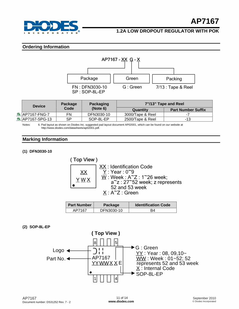
Ordering Information
AP7167 - XX G - X
PackingPackage Green
FN : DFN3030-10SP : SOP-8L-EP
G : Green 7/13 : Tape & Reel
Device Package Code
Packaging (Note 6)
7”/13” Tape and Reel Quantity Part Number Suffix
AP7167-FNG-7 FN DFN3030-10 3000/Tape & Reel -7 AP7167-SPG-13 SP SOP-8L-EP 2500/Tape & Reel -13 Notes: 6. Pad layout as shown on Diodes Inc. suggested pad layout document AP02001, which can be found on our website at
http://www.diodes.com/datasheets/ap02001.pdf.
Marking Information
(1) DFN3030-10
( Top View )
Y W X
XXXX : Identification Code
X : A~Z : Green
Y : Year : 0~9 W : Week : A~Z : 1~26 week;
a~z : 27~52 week; z represents52 and 53 week
Part Number Package Identification Code AP7167 DFN3030-10 B4
(2) SOP-8L-EP ( Top View )
AP7167 YY WW X X
LogoPart No.
58
41
E WW : Week : 01~52; 52YY : Year : 08, 09,10~G : Green
X : Internal Coderepresents 52 and 53 week
SOP-8L-EP

AP7167
1.2A LOW DROPOUT REGULATOR WITH POK
AP7167 Document number: DS31252 Rev. 7 - 2
12 of 14 www.diodes.com
September 2010 © Diodes Incorporated
Package Outline Dimensions (Continued) (1) Package Type: DFN3030-10
Bottom View
Side View
0.10 C
0.08 C Seating Plane
C
2.9/3.12.3/2.5
2.9/
3.1
0.50Typ.
1.5/
1.7
(Pin #1 ID)
AB
0.10 C A B
0.25
A
2X- 0.25 B
2X-
TOP MARK
0.50Typ.
Land Pattern Recommendation (Unit:mm)
10x-0.30
0.60
0.15
0.15
1.80
2.600.25
/0.5
5
R0.30
0.20/0.30
0.15
0/0.
02
0.57
/0.6
3
Top View
0.375Typ.
(2) Package Type: SOP-8L-EP
1.27typ 0.3/0.5
7°~9°
4.85/4.95
3.85
/3.9
5
5.90
/6.1
0
0.15/0.25
7°~9°
3.70
/4.1
0
0.62/0.82
0/0.
13 Gauge Plane0.25
4
Seating Plane
0.35
max
.
45°
Detail "A"
Detail "A"
1.30
/1.5
0
1.75
max
.
Bottom View
2.4R
ef.
3.3Ref.
Exposed pad
8x-0.60
Land Pattem Recommendation(Unit:mm)
Exposed pad
1
1
1
5.4
8x-1
.55
6x-1.27
Notes: 7. All dimensions are in millimeters. Angles are in degrees.
8. Coplanarity applies to the exposed heat sink slug as well as the terminals.
AP7167
1.2A LOW DROPOUT REGULATOR WITH POK
AP7167 Document number: DS31252 Rev. 7 - 2
13 of 14 www.diodes.com
September 2010 © Diodes Incorporated
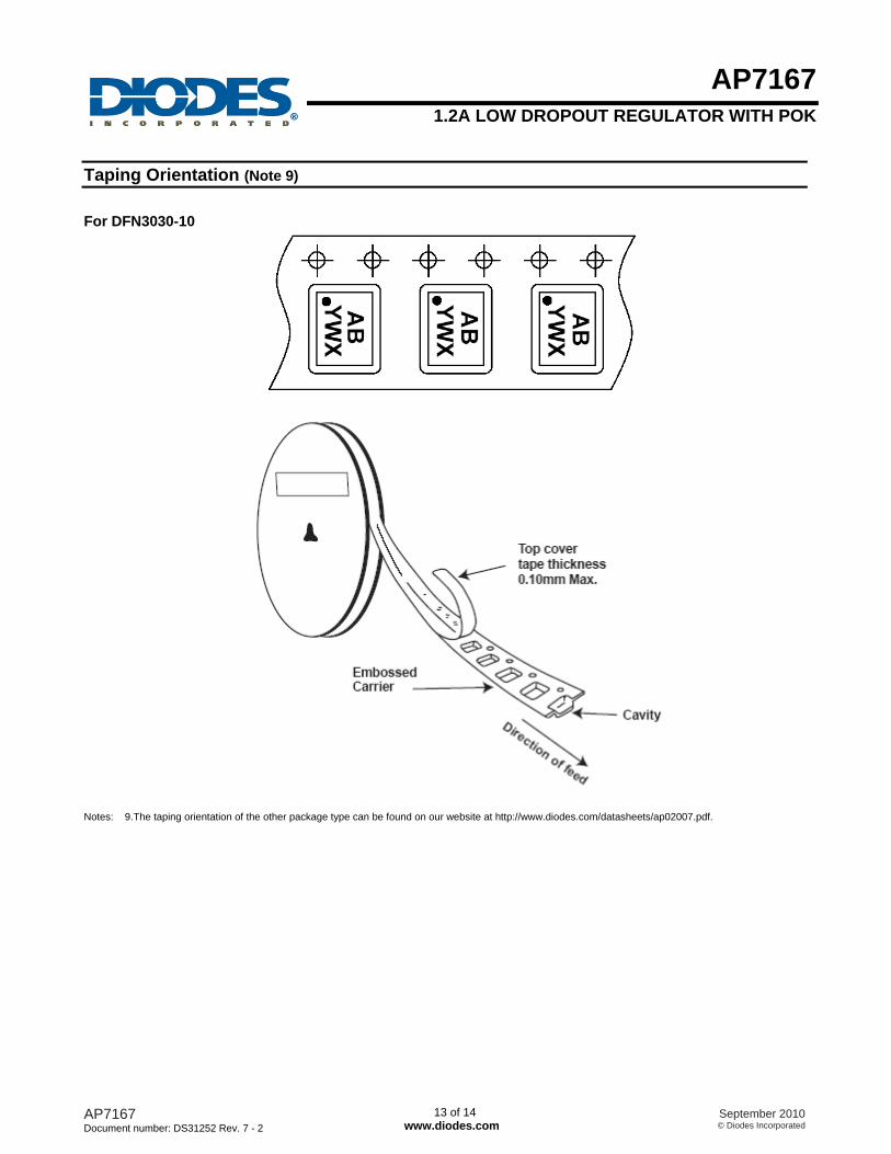
Taping Orientation (Note 9)
For DFN3030-10
Notes: 9.The taping orientation of the other package type can be found on our website at http://www.diodes.com/datasheets/ap02007.pdf.

AP7167
1.2A LOW DROPOUT REGULATOR WITH POK
AP7167 Document number: DS31252 Rev. 7 - 2
14 of 14 www.diodes.com
September 2010 © Diodes Incorporated
IMPORTANT NOTICE DIODES INCORPORATED MAKES NO WARRANTY OF ANY KIND, EXPRESS OR IMPLIED, WITH REGARDS TO THIS DOCUMENT, INCLUDING, BUT NOT LIMITED TO, THE IMPLIED WARRANTIES OF MERCHANTABILITY AND FITNESS FOR A PARTICULAR PURPOSE (AND THEIR EQUIVALENTS UNDER THE LAWS OF ANY JURISDICTION). Diodes Incorporated and its subsidiaries reserve the right to make modifications, enhancements, improvements, corrections or other changes without further notice to this document and any product described herein. Diodes Incorporated does not assume any liability arising out of the application or use of this document or any product described herein; neither does Diodes Incorporated convey any license under its patent or trademark rights, nor the rights of others. Any Customer or user of this document or products described herein in such applications shall assume all risks of such use and will agree to hold Diodes Incorporated and all the companies whose products are represented on Diodes Incorporated website, harmless against all damages. Diodes Incorporated does not warrant or accept any liability whatsoever in respect of any products purchased through unauthorized sales channel. Should Customers purchase or use Diodes Incorporated products for any unintended or unauthorized application, Customers shall indemnify and hold Diodes Incorporated and its representatives harmless against all claims, damages, expenses, and attorney fees arising out of, directly or indirectly, any claim of personal injury or death associated with such unintended or unauthorized application. Products described herein may be covered by one or more United States, international or foreign patents pending. Product names and markings noted herein may also be covered by one or more United States, international or foreign trademarks.
LIFE SUPPORT Diodes Incorporated products are specifically not authorized for use as critical components in life support devices or systems without the express written approval of the Chief Executive Officer of Diodes Incorporated. As used herein: A. Life support devices or systems are devices or systems which: 1. are intended to implant into the body, or
2. support or sustain life and whose failure to perform when properly used in accordance with instructions for use provided in the labeling can be reasonably expected to result in significant injury to the user.
B. A critical component is any component in a life support device or system whose failure to perform can be reasonably expected
to cause the failure of the life support device or to affect its safety or effectiveness. Customers represent that they have all necessary expertise in the safety and regulatory ramifications of their life support devices or systems, and acknowledge and agree that they are solely responsible for all legal, regulatory and safety-related requirements concerning their products and any use of Diodes Incorporated products in such safety-critical, life support devices or systems, notwithstanding any devices- or systems-related information or support that may be provided by Diodes Incorporated. Further, Customers must fully indemnify Diodes Incorporated and its representatives against any damages arising out of the use of Diodes Incorporated products in such safety-critical, life support devices or systems. Copyright © 2010, Diodes Incorporated www.diodes.com
![JJJJ - saurashtrauniversity.edu€¦ · JJJJ FOUR STARS (Accredited by NAAC) ;F{ZFQ8= I]lGJl;"8L SFIF",I4 I]lGJl;"8L S[d5;4 I]lGJl;"8L ZF[04 ZFHSF[8v5 . 2 JJJJ FOUR STARS (Accredited](https://img.dokumen.tips/doc/110x75/5fada83e6472a53b9710651e/jjjj-jjjj-four-stars-accredited-by-naac-fzfq8-ilgjl8l-sfifi4.jpg)


![;F{ZFQ8= I]lGJl;8L · E:\Syndicate\2016\1. Dt. 15-03-16\5. Minits.docx ~ 1 ~ ;F{ZFQ8= I]lGJl;"8L. Re-Accredited . Grade A by NAAC (CGPA 3.05) l;lg0S[8GL ;FDFgI ;EFGL SFI"JFCL GM\W](https://img.dokumen.tips/doc/110x75/5f8669782ec59e31960e114c/fzfq8-ilgjl8l-esyndicate20161-dt-15-03-165-minitsdocx-1-fzfq8.jpg)


![Karatini vved v-phil-8l[1]](https://img.dokumen.tips/doc/110x75/549bd811b47959b7318b4596/karatini-vved-v-phil-8l1.jpg)