Embed Size (px)
Citation preview

Anodic TiO2 nanotube layers: why does self-organized growth occur - A mini review
Xuemei Zhoua,
‡ Nhat Truong Nguyen
a,
‡ Selda Özkan
a, ‡ Patrik Schmuki*
ab
aDepartment of Materials Science WW4-LKO, University of Erlangen-Nuremberg, Martensstrasse 7,
91058 Erlangen, Germany
bDepartment of Chemistry, Faculty of Science, King Abdulaziz University, Jeddah, P.O. Box 80203,
Jeddah 21569, Saudi Arabia
‡These authors contributed equally.
* Corresponding author: P. Schmuki – [email protected]
Abstract
The present review gives an overview of the highlights of more than 10 years of research on synthesis
and applications of ordered oxide structures (nanotube layers, hexagonal pore arrangements) that are
formed by self-organizing anodization of metals. In particular we address the questions after the
critical factors that lead to the spectacular self-ordering during the growth of anodic oxides that finally
yield morphologies such as highly ordered TiO2 nanotube arrays and similar structures. Why are tubes
and pores formed - what are the key parameters controlling these processes?
Link to the published article: http://dx.doi.org/10.1016/j.elecom.2014.06.021

1
Over the past decade, the formation and application of anodic, self-organized TiO2 nanotube arrays
grown from a Ti metal (as illustrated in Fig.1) and similar oxide structures have attracted wide
scientific and technological interest [1-7]. Self-organization during anodization has been observed
already more than 70 years ago for aluminum that, when anodized in acidic electrolytes, forms
hexagonally ordered porous structures [8] – such ordering can peak in a virtually perfect arrangement,
as demonstrated by Masuda et al. in 1995 [9], by a meticulous optimization of the electrochemical
growth conditions. These alumina structures since then have been widely used for templating (i.e., to
fill the pores by a secondary material to form nanorods or nanowires, in combination with stripping
the template or not), as well as for numerous other applications - excellent overviews on growth and
applications of porous alumina are available; see e.g. refs. [2-4,10,11].
In the past few years, however, research activities on ordered TiO2 nanotube layers have in numbers of
paper-output surpassed porous alumina; in the past decade, more than three thousand papers have been
published dedicated to anodic TiO2 nanotubes [1,5-7]. The main reason for this enormous interest is
the anticipated impact of such nanotube layers in functional applications of titanium dioxide; such as
dye sensitized solar cells [12-15], photocatalysis [16,17] (including water splitting for the generation
of hydrogen, pollution degradation, or the reduction of CO2), biomedicine [18-20] (biomedical
coatings of implants, drug delivery systems), ion-insertion batteries, electrochromics, etc. [21-24]
These applications are, to a large extent, based on a number of almost unique features of TiO2 [1,25-
28]: it is a semiconductor of a band-gap of 3.0 eV (rutile) - 3.2 eV (anatase), with a considerably large
electron diffusion length (mainly anatase), relative band-edge positions suitable to trigger a wide range
of photocatalytic reactions; the material is highly biocompatible, and shows considerably good ion
intercalation properties. Many of these features can be exploited in a nanotubular form even more
beneficially than in powder assemblies (e.g. directional charge transport, orthogonal carrier separation,
optimized and directional diffusion profiles, defined membranes, biological cell interactions, possible
quantum size and tubular core shell devices). A particular advantage of anodic nanotube arrays is that
tubes are grown from their metallic substrate and thus can be used directly as back-contacted oxide
electrode.
While a number of excellent literature reviews exist on the immense efforts that are directed towards
an ever increasing control over growth conditions as well as exploiting the tube layers in applications
[1,5-7], only relatively little work deals with the question after the origin of self-organization in anodic
oxide formation processes [29-35]. It is thus the goal of the present review to particularly address this
point and give an overview of factors dictating self-organization and tube formation.
First reports on self-ordered TiO2 nanotube formation date back to 1984 and work by Assefpour-
Dezfuly [36] and later by Zwilling in 1999 [37] who described that the use of dilute fluoride
electrolytes in anodization of titanium can to lead to self-organizing oxide growth. Nevertheless, this
first generation of nanotubes (including later works by Grimes [38] or Beranek [39]) used acidic,
2
aqueous electrolytes, and led to tubes that showed considerable inhomogeneity in ordering, rough
walls, and a tube length limited to < 1 μm.
Experimentally significant improvements were made by introducing pH mediation [40] as well as non-
aqueous fluoride electrolytes [41-43] (mostly glycerol, ethylene glycol, DMSO, concentrated acids or
ionic liquids). Together with voltage control and -alteration procedures, this allowed to establish
smooth walled tube layers of several 100 μm thickness, bamboo or stack morphologies, branching,
diameter control in the range from 10-800 nm, and the creation of single/double walled morphologies,
for an overview, see e.g. refs [1,44,45]. It should be noted though that the as-formed tubes are
amorphous and contain significant amount of fluorides and typically carbon, and for many
applications need to be thermally crystallized to anatase or mixed anatase/rutile structures [46].
Furthermore, it is worth mentioning that using dilute fluoride electrolytes, similar aligned oxide tubes
or pore-morphologies can be grown on a full range of other metals (Zr [47-49], Hf [50], Ta [51-53], Fe
[54-56], Nb [57,58], Co [59], V [60]) and many alloys, see e.g. ref. [1] for an overview.
Factors dictating self-organization:
Classic findings on self-organization during anodic oxide growth mainly come from observations on
ordered porous alumina, and were later confirmed or adapted to self-ordered TiO2 nanotube growth:
i) Anodic oxide formation is a high field ion formation/transport process as illustrated in
Fig.1c, where ion migration is controlled by the field across the oxide layer according to
eq. )/(exp)(exp dUBABFAI , where I is the current, ΔU is the voltage across the
oxide layer thickness d defining the electric field (F = ΔU/d) and A and B are experimental
constants [61]. For a given voltage and an insoluble oxide the process is self-limiting (the
oxide grows thicker, the field drops and eventually becomes too weak to aid further ion
migration). The result is thus a compact layer of the field thickness d=f·ΔU, where f is the
oxide growth factor [f(TiO2)= 2.5 nm/V], Fig. 1b, i). A prerequisite for an extended
growth of anodic oxide is to establish an oxide formation/dissolution equilibrium. In other
words, high field conditions and thus a constant ion-flux to form permanently new oxide
can only be maintained if the steady-state oxide is thin enough. Thus a certain degree of
“solubility” of the oxide in the electrolyte is needed to provide continuous oxide growth
for building up 3D structures [1,31]. In the case of TiO2 nanotubes, this is achieved by
solvatizing TiO2 as fluoride complexes, either by chemical dissolution of the oxide or by
capturing arriving Ti4+
species (ejected to the electrolyte) by complexation as [TiF6]2-
(Fig.
1d). However, if the dissolution rate is too high no steady-state oxide layer is formed, but
complete oxide dissolution occurs (electropolishing of Ti) (Fig. 1b, ii).

3
ii) Stress: In order to explain the initial formation of a distinct tube morphology (initiated by
a curved or scalloped metal/oxide interface), mainly the buildup of compressive stress
during the early phase of anodic oxide is considered to be a key element. Stress is created
by plain volume expansion when converting metal to oxide (Pilling-Bedworth ratio) and
additionally may be enhanced by voltage induced electrostrictive forces [37,62].
Nevertheless, if there was not a continuous dissolution (see Fig. 1c), this stress (or the
induced rounding at the metal/oxide interface) would just be frozen-in in a compact oxide
layer. Experimental findings [63] such as in Fig. 2a clearly confirm the build up of net
compressive stress in the initial phase of TiO2 anodization.
iii) Field effects: Once interface curvature and oxide dissolution have started, distinct spots
will show enhanced localized dissolution due to field concentration effects (Fig. 2b) [64].
This is very well in line with work of Ono et al. [30] describing that a higher degree of
order is obtained for more rapid growth (high current densities). In particular, current
conditions close to breakdown allow ideal hexagonal ordering, as cells provide a
maximum “outward expansion pressure” (Fig. 2c) for fast growth.
iv) Typically a certain set of experimental conditions such as F- content, ΔU, pH, conductivity,
H2O content leads to a maximum organization (as indicated in Fig. 2d, where the fastest
growth results in highest degree of ordering [1,65] – note in Fig. 2d: if more drastic
conditions (higher fluoride concentration or a higher voltage than in the optimized case)
are used, the tube morphology is lost and turns either into electropolishing or sponge
formation (Fig. 2e) [66]. Maximum ordering conditions may change during anodization,
e.g. due to local acidification and ion accumulation at the tube bottoms [40,67]. Typically
the influence of different electrochemical parameters correlates well with their influence
on the steady-state oxide formation/dissolution equilibrium. Another factor that affects
morphology is the current efficiency, i.e. how much of the current goes into side reactions
– namely oxygen evolution. If oxygen evolution becomes too high, the tube morphology
turns into a sponge morphology [40,67] (Fig. 2e). A morphology change can also be
caused if too high voltages are applied – this then triggers (dielectric) breakdown events in
the oxide and, in the mildest form, leads to holes in tube walls. Therefore the formation of
a defined tube morphology is typically limited to a certain parameter range (as illustrated
in Fig. 2e).
v) Once tubes are growing their diameters can be estimated, if one assumes that from point
of oxidation, a hemispherically shaped oxide layer will grow with a radius of r=f·ΔU (f is
the anodic growth factor and ΔU is the applied potential). This simple approach is able to
explain, to a large extent, the experimentally observed linear dependencies of pore/tube
diameters on anodization voltage. (Of course, if non-aqueous, low conductivity

4
electrolytes are used, the IR-drop in the electrolyte needs to be considered to determine
the effective voltage [1]).
vi) With predefined pore initiation sites (such as induced pretexturing), the surface can guide
tube growth (most typical techniques are multiple anodization, mould indenting, or FIB
surface structuring) [68-71].
More recently, a number of fundamental quantitative approaches - namely using perturbation analysis
[32-34] or numerical treatments [72] - deal with initiation and growth of self-ordered porous alumina
and TiO2 nanotubes. In the initial phase the main question is how a morphological instability such as a
corrugated surface can be stabilized. A main conclusion from theoretical approaches (similar as in
above empirical models) is that for a certain degree of interface stress and a certain flux of ions across
the oxide interfaces (formation-dissolution equilibrium), instabilities of certain wavelength can be
stabilized (an example is shown in Fig. 3a). Under certain assumptions these models are further able to
quantitatively predict a dissolution range (expressed as oxide formation efficiency 0, as in Fig. 3b)
that needs to be established to allow for self-organizing oxide morphologies. In Fig. 3b this is shown
to hold for a range of experimental data of self-organized porous alumina and TiO2 nanotube
structures.
Nevertheless, one should point out that commonly the theoretically predicted correlation lengths often
deviate from observed tube diameters [32,33], i.e. the currently used models may be applicable to
predict the correlation length during initial layer formation (Fig. 3c) and may explain often observed
“brainy” structures at tube bottoms at high anodization voltage (Fig. 3d). The diameter of tubes during
actual growth may be better explained by a race for current, i.e. the elimination of smaller tubes (non
fitting tubes) on the account of larger ones (Fig. 3e), until a uniform hexagonal filling of space is
achieved. The diameter of the tubes then correlates well with the approach taken in Fig. 2f.
Another interesting phenomenon is that under self-organizing growth conditions, for porous alumina
and TiO2 nanotubes an unexpected lengthening during growth is observed [34,73,74]. This has been
ascribed (based on convincing experimental observations) to stress-induced viscoelastic flow of
anodic oxides [73,75] that may become possible under certain electrochemical conditions. This effect
would then contribute to pushing oxide upwards the side walls of tubes/pores (as schematically
illustrated in Fig. 1e).
The difference between a tube and a pore morphology
All above models hold essentially for porous alumina and TiO2 nanotubes. In general, alumina
anodized in acidic solution (or fluoride containing neutral solution) typically shows a nanoporous

5
structure, while for TiO2 virtually under all self-organizing conditions a tubular shape is formed [1,66].
It is important to realize that the only significant difference of the two morphologies is, if the cell
boundaries of a porous structure can be etched under the applied electrochemical conditions. As
illustrated in Fig. 1d in the case of TiO2 nanotube formation, the small fluoride ions can easily
compete with O2-
inward migration during oxide growth [76]. As a result, fluoride ions accumulate at
the metal/oxide interface and move upward with tube growth as an outer cladding (decorating the
hexagonal cell walls) [1,77]. Ti-fluoride compounds are easily dissolved in H2O (Fig. 1f) - thus the
fluoride rich locations between TiO2 tubes (or cells) are dissolved. Due to the comparably longer
etching of the tops, the resulting tubular morphology is more apparent at the top of the structure (Fig.
1a), while the bottom often still shows a tight hexagonal and porous arrangement (Fig. 1a, inset). In
case of porous alumina, even formed in fluoride electrolytes [78], a porous morphology is obtained, as
Al-fluorides are only slightly soluble in H2O.
For TiO2 the tubular shape is observed under a wide range of conditions (Fig. 2e). Only if the water
content is drastically reduced, the cell boundaries are not easily etched and porous layers can be
observed [79]. It should also be pointed out that the ratio of growth speed of the tubes versus the tube
splitting speed (that is how fast the chemical etching of the intercell fluorides follows the growing
tubes, indicated in Fig. 1f) strongly affects the tube morphology [1]. If growth is faster than splitting,
smooth tube walls are obtained, in the opposite case corrugated tube walls (bamboo type walls) are
obtained.
Specific other morphologies and factors
Above growth models and findings hold for close packed hexagonal arrangements, that is, if the
density of pore/tube initiation sites that is naturally provided or intentionally created under certain
experimental conditions is sufficiently high. If initiation occurs with a larger spacing, one may observe
individual tubes that can be considerably separated from each other [43]. Typically these tubes can
grow significantly in diameter and are embedded in a matrix of mesoporous oxide. This oxide is easier
soluble in the electrolyte and thus leads finally to an apparent larger spacing between tubes (Fig. 3f).
In the light of above arguments, the formation of such morphologies may be aided by a fast tube
splitting rate with conditions that allow for sponge formation in between tubes (O2 side reaction).
Another aspect, frequently overlooked in literature, is that anodic oxide layers often consist of a
double layer structure (oxide that is formed by O2-
inward migration and oxide formed by Ti4+
outward
migration). This leads to a twin-wall morphology of TiO2 nanotubes [46]. Typically the inner shell of
TiO2 nanotubes is of inferior quality. Only under specific conditions [44,45] or using etching
treatments this inner shell can be removed, and so-called “single-walled” tubes can be generated.
6
Concluding remarks
While in the present overview many aspects of the fascinating growth and structural features of TiO2
nanotubes and similar oxide structures could only be touched on the surface and in a referencing
manner, we hope to provide interested readers i) with a guideline through the wide literature to the
topic, and ii) more specifically, to give a comprehensive overview of critical factors affecting self-
organizing anodization.
Acknowledgements
The authors would like to acknowledge ERC, DFG and the Erlangen DFG cluster of excellence for
financial support.
7
References
[1] P. Roy, S. Berger, P. Schmuki, Angew. Chem. Int. Ed. 50 (2011) 2904.
[2] J.W. Diggle, T.C. Downie, C.W. Goulding, Chem. Rev. 69 (1969) 365.
[3] H. Asoh, S. Ono, in: G. Staikov (Ed), Electrocrystallization in Nanotechnology, Wiley-VCH:
Weinheim, 2007, pp. 138-166.
[4] G.E. Thompson, G.C. Wood, in: J.C. Scully (Ed), Treatise on Materials Science and Technology,
Vol. 23, Corrosion: Aqueous Processed and Passive Films, Academic Press, New York, 1983, pp.
205-329.
[5] D. Kowalski, D. Kim, P. Schmuki, Nano Today 8 (2013) 235.
[6] Y.R. Smith, R.S. Ray, K. Carlson, B. Sarma, M. Misra, Materials 6 (2013) 2892.
[7] D. Regonini, C.R. Bowen, A. Jaroenworaluck, R. Stevens, Mater. Sci. Eng. R 74 (2013) 377.
[8] T. Rummel, Z. Phys., 99 (1936) 518.
[9] H. Masuda, K. Fukuda, Science 268 (1995) 1466.
[10] J.Y. Liang, H. Chik, J.M. Xu, IEEE J. Sel. Top. Quantum Electron. 8 (2002) 998.
[11] B.B. Lakshmi, P.K. Dorhout, C.R. Martin, Chem. Mater. 9 (1997) 857.
[12] P. Roy, D. Kim, K. Lee, E. Spiecker, P. Schmuki, Nanoscale 2 (2010) 45.
[13] J.R. Jennings, A. Ghicov, L.M. Peter, P. Schmuki, A.B. Walker, J. Am. Chem. Soc. 130 (2008)
13364.
[14] K. Shankar, J.I. Basham, N.K. Allam, O.K. Varghese, G.K. Mor, X. Feng, M. Paulose, J.A.
Seabold, K.-S. Choi, C.A. Grimes, J. Phys. Chem. C 113 (2009) 6327.
[15] K. Zhu, N.R. Neale, A. Miedaner, A.J. Frank, Nano Lett. 7 (2007) 69.
[16] I. Paramasivam, H. Jha, N. Liu, P. Schmuki, Small 8 (2012) 3073.
[17] T. Ochiai, A. Fujishima, Photochem. Photobio. C: Photochem. Rev. 13 (2012) 247.
[18] S. Bauer, P. Schmuki, K. von der Mark, J. Park, Prog. Mater. Sci. 58 (2013) 261.
[19] J. Park, S. Bauer, K. von Der Mark, P. Schmuki, Nano Lett. 7 (2007) 1686.
[20] S. Oh, K.S. Brammer, Y.S.J. Li, D. Teng, A.J. Engler, S. Chien, S. Jin, Proc. Natl. Acad. Sci.
USA 106 (2009) 2130.
[21] A. Ghicov, H. Tsuchiya, R. Hahn, J.M. Macak, A.G. Muñoz, P. Schmuki, Electrochem. Commun.
8 (2006) 528.
[22] D. Fang, K. Huang, S. Liu, Z. Li, J. Alloys Compd. 464 (2008) L5.
[23] H. Xiong, H. Yildirim, E.V. Shevchenko, V.B. Prakapenka, B. Koo, M.D. Slater, M.
Balasubramanian, S.K.R.S. Sankaranarayanan, J.P. Greeley, S. Tepavcevic, N.M. Dimitrijievic, P.
Podsiadlo, C.S. Johnson, T.J. Rajh, J. Phys. Chem. C 116 (2012) 3181.
[24] W. Wei, G. Oltean, C.-W. Tai, K. Edström, F. Björefors, L. Nyholm, J. Mater. Chem. A 1 (2013)
8160.
[25] U. Diebold, Surf. Sci. Rep. 48 (2003) 53.
[26] A.L. Linsebigler, G. Lu, J.T. Yates, Chem. Rev. 95 (1995) 735.

8
[27] X. Chen, C. Li, M. Grätzel, R. Kostecki, S.S. Mao, Chem. Soc. Rev. 41 (2012) 7909.
[28] A. Fujishima, X. Zhang, D.A. Tryk, Surf. Sci. Rep. 63 (2008) 515.
[29] J.P. O’Sullivan, G.C. Wood, Proc. R. Soc. Lond. A 317 (1970) 511.
[30] S. Ono, M. Saito, H. Asoh, Electrochim. Acta 51 (2005) 827.
[31] K.R. Hebert, S. Albu, I. Paramasivam, P. Schmuki, Nat. Mater. 11 (2012) 162.
[32] G.K. Singh, A.A. Golovin, I.S. Aranson, Phys. Rev. B 73 (2006) 205422.
[33] L.G. Stanton, A.A. Golovin, Phys. Rev. B 79 (2009) 035414.
[34] S.J. Garcia-Vergara, L. Iglesias-Rubianes, C.E. Blanco-Pinzon, P. Skeldon, G.E. Thompson, P.
Campestrini, Proc. R. Soc. A 462 (2006) 2345.
[35] O. Jessensky, F. Muller, U. Gösele, Appl. Phys. Lett. 72 (1998) 1173.
[36] M. Assefpour-Dezfuly, C. Vlachos, E.H. Andrews, J. Mater. Sci. 19 (1984) 3626.
[37] V. Zwilling, E. Darque-Ceretti, A. Boutry-Forveille, D. David, M. Y. Perrin, M. Aucouturier,
Surf. Interface Anal. 27 (1999) 629.
[38] D. Gong, C.A. Grimes, O.K. Varghese, W.C. Hu, R.S. Singh, Z. Chen, E.C. Dickey, J. Mater.
Res. 16 (2001) 3331.
[39] R. Beranek, H. Hildebrand, P. Schmuki, Electrochem. Sol. Stat. Lett. 6 (2003) B12.
[40] J.M. Macak, H. Tsuchiya, P. Schmuki, Angew. Chem. Int. Ed. 44 (2005) 2100.
[41] J.M. Macak, H. Tsuchiya, L. Taveira, S. Aldabergerova, P. Schmuki, Angew. Chem. Int. Ed. 44
(2005) 7463.
[42] M. Paulose, K. Shankar, S. Yoriya, H.E. Prakasam, O.K. Varghese, G.K. Mor, T.A. Latempa, A.
Fitzgerald, C.A. Grimes, J. Phys. Chem. B 110 (2006) 16179.
[43] S.P. Albu, P. Schmuki, Phys. Status Solidi RRL 4 (2010) 215.
[44] H. Mirabolghasemi, N. Liu, K. Lee, P. Schmuki, Chem. Commun. 49 (2013) 2067.
[45] N. Liu, H. Mirabolghasemi, K. Lee, S.P. Albu, A. Tighineanu, M. Altomare, P. Schmuki, Faraday
Discuss. 164 (2013) 107.
[46] S.P. Albu, A. Ghicov, S. Aldabergenova, P. Drechsel, D. LeClere, G.E. Thompson, J.M. Macak,
P. Schmuki, Adv. Mater. 20 (2008) 4135.
[47] H. Tsuchiya, J. M. Macak, L. Taveira, P. Schmuki, Chem. Phys. Lett., 410 (2005) 188.
[48] H. Tsuchiya, J. M. Macak, L. Taveira, P. Schmuki, ECS Trans. 1 (2006) 351.
[49] S. Berger, F. Jakubka, P. Schmuki, Electrochem. Commun. 10 (2008) 1916.
[50] H. Tsuchiya, P. Schmuki, Electrochem. Commun. 7 (2005) 49.
[51] I. Sieber, B. Kannan, P. Schmuki, Electrochem. Solid-State Lett. 8 (2005) J10.
[52] I.V. Sieber, P. Schmuki, J. Electrochem. Soc. 152 (2005) C639.
[53] H.A. El-Sayed, V.I. Birss, Nano Lett. 9 (2009) 1350.
[54] S.P. Albu, A. Ghicov, P. Schmuki, Phys. Status Solidi RRL 3 (2009) 64.
[55] T.D. Burleigh, P. Schmuki, S. Virtanen, J. Electrochem. Soc. 156 (2009) C45.
[56] S. K. Mohapatra, S. E. John, S. Banerjee, M. Misra, Chem. Mater. 21 (2009) 3048.

9
[57] I. Sieber, H. Hildebrand, A. Friedrich, P. Schmuki, Electrochem. Commun. 7 (2005) 97.
[58] W. Wei, K. Lee, S. Shaw, P. Schmuki, Chem. Commun. 48 (2012) 4244.
[59] C.-Y. Lee, K. Lee, P. Schmuki, Angew. Chem. Int. Ed. 52 (2013) 2077.
[60] Y. Yang, S.P. Albu, D. Kim, P. Schmuki, Angew. Chem. Int. Ed. 50 (2011) 9071.
[61] A. Güntherschulze, H. Betz, Z. Phys. 92 (1934) 367.
[62] J.-F. Vanhumbeeck, J. Proost, Electrochim. Acta 53 (2008) 6165.
[63] J.F. Vanhumbeeck, J. Proost, 209th ECS Meeting 2006, abstract 432.
[64] O. Jessensky, F. Muller, U. Gösele, Appl. Phys. Lett. 72 (1998) 1173.
[65] S.P. Albu, A. Ghicov, J.M. Macak, P. Schmuki, Phys. Status Solidi RRL 1 (2007) R65.
[66] S.P. Albu, P. Roy, S. Virtanen, P. Schmuki, Isr. J. Chem. 50 (2010) 453.
[67] K. Yasuda, J.M. Macak, S. Berger, A. Ghicov, P. Schmuki, J. Electrochem. Soc. 154 (2007)
C472.
[68] J.M. Macak, S.P. Albu, P. Schmuki, Phys. Status Solidi RRL 1 (2007) 181.
[69] D. Wang, B. Yu, C. Wang, F. Zhou, W. Liu, Adv. Mater. 21 (2009) 1964.
[70] B. Chen, K. Lu, Langmuir 27 (2011) 12179.
[71] B. Chen, K. Lu, J.A. Geldmeier, Chem. Comm. 47 (2011) 10085.
[72] J.E. Houser, K.R. Hebert, Nat. Mater. 8 (2009) 415.
[73] S. Berger, J. Kunze, P. Schmuki, D. LeClere, A.T. Valota, P. Skeldon, G.E. Thompson,
Electrochim. Acta 54 (2009) 5942.
[74] S.P. Albu, P. Schmuki, Electrochim. Acta 91 (2013) 90.
[75] P. Skeldon, G.E. Thompson, S.J. Garcia-Vergara, L. Iglesias-Rubianes, C.E. Blanco-Pinzon,
Electrochem. Solid-State Lett. 9 (2006) B47.
[76] H. Habazaki, K. Fushimi, K. Shimizu, P. Skeldon, G.E. Thompson, Electrochem. Commun. 9
(2007) 1222.
[77] S. Berger, S.P. Albu, F. Schmidt-Stein, H. Hildebrand, P. Schmuki, J.S. Hammond, D.F. Paul, S.
Reichlmaier, Surf. Sci. 605 (2011) L57.
[78] H. Tsuchiya, S. Berger, J.M. Macak, A.G. Muñoz, P. Schmuki, Electrochem. Commun. 9 (2007)
545.
[79] W. Wei, S. Berger, C. Hauser, K. Meyer, M. Yang, P. Schmuki, Electrochem. Commun. 12
(2010) 1184.
10
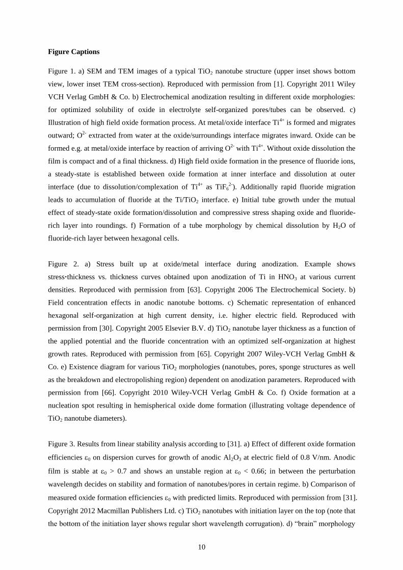
Figure Captions
Figure 1. a) SEM and TEM images of a typical TiO2 nanotube structure (upper inset shows bottom
view, lower inset TEM cross-section). Reproduced with permission from [1]. Copyright 2011 Wiley
VCH Verlag GmbH & Co. b) Electrochemical anodization resulting in different oxide morphologies:
for optimized solubility of oxide in electrolyte self-organized pores/tubes can be observed. c)
Illustration of high field oxide formation process. At metal/oxide interface Ti4+
is formed and migrates
outward; O2-
extracted from water at the oxide/surroundings interface migrates inward. Oxide can be
formed e.g. at metal/oxide interface by reaction of arriving O2-
with Ti4+
. Without oxide dissolution the
film is compact and of a final thickness. d) High field oxide formation in the presence of fluoride ions,
a steady-state is established between oxide formation at inner interface and dissolution at outer
interface (due to dissolution/complexation of Ti4+
as TiF62-
). Additionally rapid fluoride migration
leads to accumulation of fluoride at the Ti/TiO2 interface. e) Initial tube growth under the mutual
effect of steady-state oxide formation/dissolution and compressive stress shaping oxide and fluoride-
rich layer into roundings. f) Formation of a tube morphology by chemical dissolution by H2O of
fluoride-rich layer between hexagonal cells.
Figure 2. a) Stress built up at oxide/metal interface during anodization. Example shows
stress·thickness vs. thickness curves obtained upon anodization of Ti in HNO3 at various current
densities. Reproduced with permission from [63]. Copyright 2006 The Electrochemical Society. b)
Field concentration effects in anodic nanotube bottoms. c) Schematic representation of enhanced
hexagonal self-organization at high current density, i.e. higher electric field. Reproduced with
permission from [30]. Copyright 2005 Elsevier B.V. d) TiO2 nanotube layer thickness as a function of
the applied potential and the fluoride concentration with an optimized self-organization at highest
growth rates. Reproduced with permission from [65]. Copyright 2007 Wiley-VCH Verlag GmbH &
Co. e) Existence diagram for various TiO2 morphologies (nanotubes, pores, sponge structures as well
as the breakdown and electropolishing region) dependent on anodization parameters. Reproduced with
permission from [66]. Copyright 2010 Wiley-VCH Verlag GmbH & Co. f) Oxide formation at a
nucleation spot resulting in hemispherical oxide dome formation (illustrating voltage dependence of
TiO2 nanotube diameters).
Figure 3. Results from linear stability analysis according to [31]. a) Effect of different oxide formation
efficiencies 0 on dispersion curves for growth of anodic Al2O3 at electric field of 0.8 V/nm. Anodic
film is stable at 0 > 0.7 and shows an unstable region at 0 < 0.66; in between the perturbation
wavelength decides on stability and formation of nanotubes/pores in certain regime. b) Comparison of
measured oxide formation efficiencies 0 with predicted limits. Reproduced with permission from [31].
Copyright 2012 Macmillan Publishers Ltd. c) TiO2 nanotubes with initiation layer on the top (note that
the bottom of the initiation layer shows regular short wavelength corrugation). d) “brain” morphology
11
on bottom of anodic TiO2 nanotubes grown at high currents (bottom shows short wavelength
corrugation). e,f) Schematic illustration for the growth of TiO2 nanotubes with e) high and f) low
initiation nucleation density leading to growth of small tube exclusion and dense hexagonal packing (e)
or single tube bulbs in a porous matrix (f), respectively.

12
Figure 1.

13
Figure 2.

14
Figure 3.