Embed Size (px)
Citation preview

ANNUAL REPORT 1998UNSW
PHOTOVOLTAICS GROUP
ANNUAL REPORT 1998UNSW
PHOTOVOLTAICS GROUP

THE UNIVERSITY OFNEW SOUTH WALES
THE PHOTOVOLTAICS SPECIAL RESEARCH CENTREIS A SPECIAL RESEARCH CENTRE OF THE AUSTRALIAN RESEARCH COUNCIL
THE KEY CENTRE FOR PHOTOVOLTAIC ENGINEERINGIS A KEY CENTRE OF THE AUSTRALIAN RESEARCH COUNCIL
Cover Photo: Wind, Solar Powered Car & Building (G8 Building at Birmingham,Photo Courtesy of David Shepherd, BP Solar)

ANNUAL REPORT 1998
UNSWPHOTOVOLTAICS GROUP
(Incorporating The 1998 Annual Report of the PHOTOVOLTAICS SPECIAL RESEARCHCENTRE and Introducing the KEY CENTRE FOR PHOTOVOLTAIC ENGINEERING)
Photovoltaics GroupSchool of Electrical EngineeringUniversity of New South Wales
Sydney NSW 2052AUSTRALIA
Tel +61 2 9385 4018 Fax +61 2 9662 4240E-mail: [email protected]: http://www.pv.unsw.edu.au


C O N T E N T S
1998 HIGHLIGHTS PHOTOVOLTAICS SPECIAL RESEARCH CENTRE 6
DIRECTOR’S REPORT (PHOTOVOLTAICS SPECIAL RESEARCH CENTRE) 8
DIRECTOR’S REPORT (KEY CENTRE FOR PHOTOVOLTAIC ENGINEERING) 9
FACILITIES AND STRUCTURE 10
PHOTOVOLTAICS SPECIAL RESEARCH CENTRE RESEARCH REPORTS 12
HIGH EFFICIENCY SILICON SOLAR CELLS 12
THEORY AND MODELLING 15
THIN FILM SOLAR CELLS 17
BURIED CONTACT SOLAR CELLS 21
ELECTRICITY INDUSTRY RESTRUCTURING & REGULATION 24
SYSTEM HARDWARE AND PERFORMANCE MONITORING 24
EDUCATION AND EXTERNAL ACTIVITIES 26
EDUCATION AND EXTERNAL ACTIVITIES 26
EXTERNAL RELATIONS 29
DESIGN ASSISTANCE DIVISION 30
KEY CENTRE FOR PHOTOVOLTAIC ENGINEERING REPORTS 16
BACKGROUND 16
COMMERCIAL RESEARCH 16
TEACHING 16
CONTRACTS, PROFESSIONAL ACTIVITIES AND TECHNOLOGY TRANSFER 38
BUSINESS DEVELOPMENTS 38
CONTRACTS AND AGREEMENTS 39
TECHNOLOGY TRANSFER 40
PHOTOVOLTAIC SPECIAL RESEARCH CENTRE FINANCES 42
1998 PUBLICATIONS 44
APPENDIX A 48
PHOTOVOLTAICS SPECIAL RESEARCH CENTRE ADVISORY COMMITTEE 48
APPENDIX B 49
PHOTOVOLTAICS SPECIAL RESEARCH CENTRE PERSONNEL 49
5
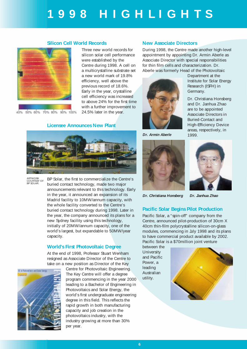
New Associate DirectorsDuring 1998, the Centre made another high-levelappointment by appointing Dr. Armin Aberle asAssociate Director with special responsibilitiesfor thin film cells and characterization. Dr.Aberle was formerly Head of the Photovoltaic
Department at theInstitute for Solar EnergyResearch (ISFH) inGermany.
Dr. Christiana Honsbergand Dr. Jianhua Zhaoare to be appointedAssociate Directors inBuried-Contact andHigh-Efficiency Deviceareas, respectively, in1999.
6
1 9 9 8 H I G H L I G H T S
Silicon Cell World RecordsThree new world records forsilicon solar cell performancewere established by theCentre during 1998. A cell ona multicrystalline substrate seta new world mark of 19.8%efficiency, well above theprevious record of 18.6%.Early in the year, crystallinecell efficiency was increasedto above 24% for the first timewith a further improvement to24.5% later in the year.
World’s First Photovoltaic DegreeAt the end of 1998, Professor Stuart Wenhamresigned as Associate Director of the Centre totake on a new position as Director of the Key
Centre for Photovoltaic Engineering.The Key Centre will offer a degreeprogram commencing in the year 2000leading to a Bachelor of Engineering inPhotovoltaics and Solar Energy, theworld’s first undergraduate engineeringdegree in this field. This reflects therapid growth in both manufacturingcapacity and job creation in thephotovoltaics industry, with theindustry growing at more than 30%per year.
ARTWORKCOURTESY OFBP SOLAR.
BP Solar, the first to commercialize the Centre’sburied contact technology, made two majorannouncements relevant to this technology. Earlyin the year, it announced an expansion of itsMadrid facility to 10MW/annum capacity, withthe whole facility converted to the Centre’sburied contact technology during 1998. Later inthe year, the company announced its plans for anew Sydney facility using this technology,initially of 20MW/annum capacity, one of theworld’s largest, but expandable to 50MW/yearcapacity.
Licensee Announces New Plant
Pacific Solar Begins Pilot ProductionPacific Solar, a “spin-off” company from theCentre, announced pilot-production of 30cm X40cm thin-film polycrystalline silicon-on-glassmodules, commencing in July 1998 and its plansto have commercial product available by 2002.Pacific Solar is a $70million joint venturebetween theUniversityand PacificPower, aleadingAustralianutility.
Dr. Armin Aberle
Dr. Christiana Honsberg Dr. Jianhua Zhao

7
Centre Accredited ISO9001 QualityStandardIn November 1998 the “Advanced Cell Division”of the Centre achieved accreditation toInternational Quality Standard ISO9001 “QualitySystems-Model for quality assurance in design,development, production, installation andservicing”. The Centre was one of the first groupswithin an Australian University to receive suchaccreditation.
Brendon Vandenberg and Mark Silver with theCentre's ISO9001 accreditation certificates.
At the end of 1998, Professors Martin Green andStuart Wenham, Centre Director and formerAssociate Director, were advised that they wereto be awarded the 1999 Australia Prize for theiroutstanding achievements in energy science andtechnology, the first all-Australian team toreceive this award since 1992. The prize is aninternational award for specific achievement in aselected area of science and technologypromoting human welfare. It was presented bythe Prime Minister, The Honourable JohnHoward, during a special ceremony atParliament House in February 1999.
Other Major AwardsIn February 1998, the Centre received theprestigious Chairman's Award at the 1998Australian Technology Awards shared jointlywith its “spin-off” Pacific Solar Pty. Ltd. Theaward, for the “one most excellent project,regardless of its nominated category” recognizedthe outstanding success in bringing thin-filmpolycrystalline silicon-on-glass cells to the stageof commercial readiness.
1999 Australia Prize
P H O T O V O L T A I C S S P E C I A LR E S E A R C H C E N T R E
In July 1998, a paper on the role of “excitons” incell operation by Centre Director, Martin Green,won the overall best poster paper award at the2nd World Conference on Photovoltaic SolarEnergy Conversion in Vienna, the largestconference ever in this field, from the over 1,000posters submitted.
Centre’s Business and Technology Manager MarkSilver with the Australian Technology Award.
Professor Stuart Wenham (left), the Prime Ministerand Professor Martin Green at Parliament House.

The Photovoltaics Special ResearchCentre at the University of NewSouth Wales (UNSW) wasestablished in 1990 to developphotovoltaic technology into asustainable power generationoption for the future. Photovoltaicor “solar” cells convert sunlightdirectly into electricity usingquantum-mechanical interactionsbetween this light and electrons inthe semiconductor material used tomake the cell.
If this technology is to displace lessenvironmentally desirable coal-fired and nuclearpower plants, the cost of photovoltaics must bereduced, the energy conversion efficiencyimproved and new applications for the cellsdeveloped.
The UNSW Photovoltaics Special ResearchCentre is at the forefront of international efforts inaddressing these three key areas. The 1998 yearcovered by this report was again a year duringwhich the Centre demonstrated outstandingachievements across all three of its key researchareas.
Continued International GrowthThe rapid growth rate of the internationalphotovoltaic industry noted during 1997 waslargely sustained during 1998 with 30% growthreported. Residential rooftop programs in Japan,Europe and the USA drove this growth, with over10 GW of photovoltaics targeted for suchapplications by 2010.
1998 Centre HighlightsThe major results achieved by the Centre arehighlighted on the previous page. It would seemthat 1998, the penultimate year of the Centre’soperation, has been the most successful yetacross the whole range of Centre activities. Not
8
D I R E C T O R ’ S R E P O R T S
only did the Centre continue to lead the world inhigh efficiency solar cell research, its licenseeshad outstanding success in commercializingCentre technology. Centre staff received severalprestigious local and international awards andthe professionalism of its activities wasdocumented by ISO9001 accreditation.
Key CentreRecognizing the rapid growth of thephotovoltaics industry and its need for trainedstaff, a Key Centre for Teaching and Research inPhotovoltaic Engineering was awarded to theUniversity, commencing in early 1999. This KeyCentre will offer the world’s first undergraduateprogram in Photovoltaics and Solar Energy,beginning in the year 2000. Professor StuartWenham resigned from Associate Directorship ofthe Special Research Centre at the end of 1998 totake on the role of Director of the Key Centre.As detailed in Professor Wenham’saccompanying report and elsewhere in thisvolume, the Key Centre will initiate strong newprograms, particularly in the undergraduate andpostgraduate teaching areas and in industry-initiated research.
Prospects for Beyond 1999The Special Research Centre is entering its finalyear of operation and is due to terminate at theend of 1999. Mechanisms are being sought toallow the continuation of the Centre’s basicresearch activities and maintenance of thefundamental processing capabilities developedduring the Centre’s operation. Invariably, aconsiderable winding-down of Centre activities isanticipated during the second half of 1999 toaccommodate the reduced resources likely to beavailable past this date.
I thank all staff and collaborators for theircontributions during 1998 and wish them wellfor the coming year.
Professor Martin A. Green,Director,Photovoltaics Special Research Centre.
DIRECTOR’S REPORT(Photovoltaics Special Research Centre)
An exciting newera has dawned forthe photovoltaicindustry with rapidgrowth of between30 - 40% perannum in recentyears creating newneeds and rapidevolution. Some ofthe outcomesinclude massiveincreases in
production capacity, demands for new oradapted technology and a growing need fortrained engineers. These are stimulating newactivities for the UNSW Photovoltaics Group. Inparticular, in the research area, several newcollaborative research projects are to be or havebeen established with industry while in theeducational area, our group will be establishingthe world’s first undergraduate engineeringdegree in Photovoltaics and Solar Energy,commencing in the year 2000.
The strong track record of the photovoltaicsgroup in conjunction with the rapidly evolvingneeds of the photovoltaic industry has led to theestablishment of a Key Centre for Teaching andResearch in the photovoltaics area, funded by theAustralian Research Council. This new Centre isfunded for a period of six years, with one of theprimary aims being to become self-sustaining bythe end of the funding period. This is one ofonly eight Key Centres awarded Australia-wideacross all disciplines, indicating the growingimportance of photovoltaics and Australia’sinternational leadership in the area. Australianmanufacturers are already the largest per-capitaworldwide, with the market share expected tocontinue to increase in the future.
The new educational initiatives of the Key Centrerequire the development of a range of new andinnovative teaching aids and materials, many ofwhich will be multimedia interactive CD-basedpresentations. Increasing emphasis will beplaced on offering web-based courses via theinternet and a promotional CD is to be producedto portray the calibre and scope of our courses.In the new degree program, considerableimportance will be placed on providing students
9
with hands-on experience with photovoltaicdevices, modules and systems. The program willalso cover the more general solar energy areaand will provide students with a grounding inother renewable energy technologies, such as theuse of wind generators, biomass and solarthermal systems.
The new industry-initiated research programs forthe Key Centre cover a range of areas thatincludes thin film technology, conventional bulkdevices, new generations of bulk technology,and photovoltaic systems research thatparticularly focuses on grid interconnection.With licensees of UNSW technology nowincluding companies from most major countries,it is anticipated that new collaborative researchprograms will be established on an ongoing basisto suit the particular needs of each individualcompany, such as with regard to chosensubstrate type and infrastructural/equipmentconstraints.
For the first time, our Centre is planning toembark upon training courses in photovoltaicprocessing in the areas of high efficiency devicesand our commercially successful buried contactsolar cell. In the past, such material has beendisseminated only through technology transfersto licensees, but with most major manufacturersnow licensees of UNSW technology, the abovecourses may form an essential ingredient in thetraining of all new photovoltaics researchers andengineers internationally.
The Key Centre activities focus primarily in twoareas: collaborative research with industry that isconducted on a full incremental cost recoverybasis; and teaching where the primary newinitiative is the world’s first bachelor ofengineering in Photovoltaics and Solar Energy.The latter is also being strongly supported by theSustainable Energy Development Authority(SEDA) and The University of New South Wales.
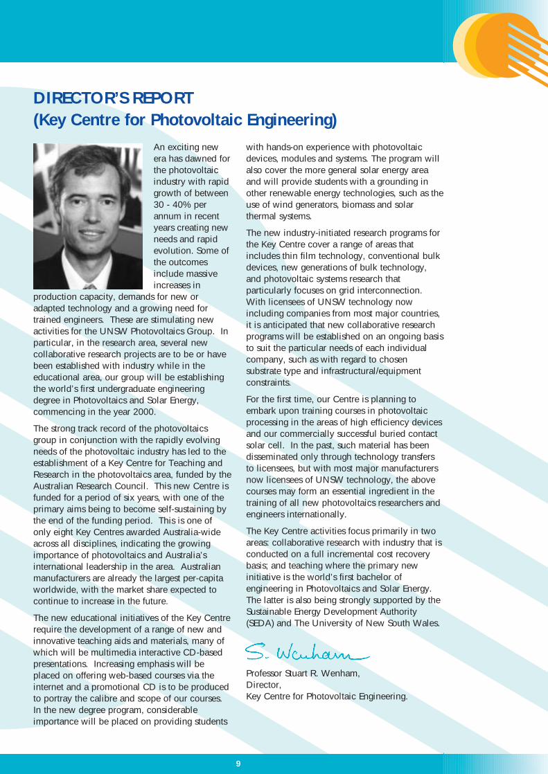
Professor Stuart R. Wenham,Director,Key Centre for Photovoltaic Engineering.
DIRECTOR’S REPORT(Key Centre for Photovoltaic Engineering)

The Centre’s three major work areas arethe Photovoltaics Research Laboratory,the Device Characterization Area andthe Power Electronics Laboratory.Systems work is also undertaken at theLittle Bay Research Facility.
Photovoltaics ResearchLaboratoryThe Centre boasts the largestand most sophisticated bulksilicon solar cell researchfacility in Australia.Laboratory space of 430 m2 islocated on 4 floors of theSchool of ElectricalEngineering building and isserviced with filtered andconditioned air, appropriatecooling water, processing gas,de-ionized water supply,chemical fume cupboards andexhausts. There is anadditional 474 m2 area
immediately adjacent to the laboratories for theaccommodation of staff, research students andlaboratory support facilities. Off site, areastotalling 200 m2 are used for the storage ofchemicals and equipment spare parts.
The laboratory is furnished with a range ofprocessing and characterisation equipment
including 37 diffusionfurnaces, 5 vacuumdeposition systems, 3laser scribingmachines,ellipsometer,microwave carrierlifetime system, rapidthermal annealer, fourpoint sheet resistivityprobe, quartz tubewasher, silver, nickeland copper platingunits, infrared andvisible wavelengthmicroscopes, 3 wafermask aligners, spin on
diffusion system, automated photoresist dualtrack coater, photoresist spinner, ion implantater,reactive ion etcher, electron beam and sputterdeposition systems, and a laboratory systemcontrol and data acquisition monitoring system.
10
F A C I L I T I E S A N D S T R U
Laboratory facilities are available for the growthof silicon films on both silicon and foreignsubstrates. Related services are also availablethrough the Department of Electronicslaboratories which are partly supported by theCentre. Additional facilities available in the latterlaboratories include wafer prober and bondersand computer aided design for mask layout.
The PVSRC also owns equipment and has accessto the new SNF, Semiconductor NanofabricationFacility, this is a joint facility between Physicsand Electrical Engineering and houses amicroelectronics laboratory and ananofabrication laboratory for e-beamlithography.
Additional equipment is available on theUniversity campus, which is commonly used forcell work. Included in this category are electronmicroscopes, X-ray diffraction, surface analysisand photoluminescence equipment.
A computer network of 46 PCs, 1 Novell Server,1 NT Server, 1 Intranet Server, 4 Macintosh, 1Unix workstation and 1 Unix computer serversupport the device laboratory, simulation andCentre administrative activities. Another 20 PCsare dedicated for the computer control oflaboratory equipment.
The device laboratories, Characterisation Areaand adjacent facilities operate 24 hours per day,365 days per year and are developed andmaintained by the Laboratory Development andOperations Team. In 1998, the team, under theleadership of Mark Silver, comprised 6 full timeand 2 part time employees, which includeelectrical, mechanical and industrial designengineers and technicians, a physicist, computerand network manager and administrative staff.
Over $0.5M has been earmarked for the upgradeof laboratory infrastructure such as exhaust andfume cupboards for 1999.
Device Characterization AreaSpace in the basement of the ElectricalEngineering Building was made available to theCentre by the University in 1995. The spacecontains a reception area, seminar room, library,offices for Centre staff interacting with the publicand industry, including the Business &Technology Manager and Design AssistanceDivision Manager, computer workstations for thedevice modelling activities of the Centre, and theDevice Characterization Area.
Figure 1:Location Map.
Figure 2:Layout of theCentre withinthe ElectricalEngineeringBuilding.

The Device Characterization Area housescharacterization equipment including “DarkStar”, the Centre’s station for temperaturecontrolled dark current-voltage measurements,the Centre’s Fourier Transform InfraredSpectroscopy system, Admittance Spectroscopysystem, Ellipsometer, photoconductance decayequipment, infrared microscope and equipmentfor spectral response and related opticalmeasurements.
Power Electronics LaboratoryThis 40 m2 laboratory is equipped with a range ofpower supplies for heavy current testing of DC-DC converters and inverters including a 60 Vbattery bank for remote area power supplytesting. A range of test equipment is availableincluding: high frequency oscilloscopes; trueRMS meters up to 2 MHz response; currentprobes up to 1000 A and all the usual smallmetering equipment. The laboratory also has anumber of microprocessor/microcontrollerdevelopment systems which include TMS320C25, and 80C196 systems which areparticularly suited to power electronicapplications. IBM-PC compatibles provideanalysis software and printed circuit design andplotting systems. The laboratory also has accessto programming facilities for a large range ofprogrammable logic arrays.
Little Bay FacilityThe Little Bay solar energy research facility(approximately 10 minutes drive from the mainUniversity campus) has been operating a gridconnected PV system for over four years. Theinitial installation at the facility included a 3.8kW array, battery systems and inverterconnected to the local grid. Currently we have3.8kW of BP and Solarex crystalline siliconarrays and a further 1kW of Canonamorphous silicon array (see Figure3). These arrays are patchable to alarge range of series-parallelconfigurations and are used forevaluating a variety of systems underactual operating conditions.
All the systems are being monitoredby an extensive data acquisitionsystem which logs environmental andelectrical conditions of the systemsunder test.
11
A single axis tracking module test facility is alsoinstalled. Each module is connected to anelectronic load which enables a completecurrent / voltage characteristic to be obtained. Adata acquisition computer system controls theelectronic loads and logs environmentalconditions, module temperatures and electricalcharacteristics of the modules under test. Thetracking system may be fixed in orientation ortracked to investigate module performance underboth conditions.
C T U R E
Figure 3: BP,Solarex, andCanon arrays atLittle Bay.
Figure 4: Functional organization of thePhotovoltaics Special Research Centrefor 1999.
A range of other test equipment is availableincluding a Voltec PM3000A harmonic analyserfor investigating quality of supply issues for bothRAPS and grid connected systems and a highspeed data acquisition system for investigatingprotection issues related to grid connectedsystems.

High EfficiencySilicon Solar CellsSenior Project Scientist:Dr. Jianhua Zhao (project leader)
University Staff:Prof. Martin Green, Prof. Stuart Wenham
Project Scientist: Dr. Aihua Wang
Visiting Fellow: P. Altermatt
Researcher: Fei Yun
1998 Objective - Improving PERL CellEfficienciesThe major objective in 1998 for the highefficiency group was to further improve theefficiency of PERL (passivated emitter, rearlocally-diffused) cells and modules, and also todemonstrate high performance onmulticrystalline silicon substrates. The 1998objective for the high efficiency group has beenfulfilled with the demonstration of 3 new worldrecord performances by mono-crystalline and multi-crystallinesilicon cells. Another recordmatching performance was alsodemonstrated by a photovoltaicmodule with PERL cells.
Improved High EfficiencyPERL CellsFigure 5 shows the PERL cell structure, whichhad previously demonstrated a record AM1.5efficiency of 24.0% for silicon cells in 1994. In1998, the PERL cells have been redesigned toreduce the metallisation shading loss and metalresistance loss.
12
P H O T O V O L T A I C S
The history of the efficiency evolution for siliconsolar cells is shown Figure 6. With the new celldesigns, the efficiency records of silicon solarcells were broken twice by PERL cells fabricatedat the Centre in 1998. The picture frame cellsdemonstrated 24.4% efficiency in February, 1998and 24.5% in December, 1998.
Figure 5: Passivated Emitter, Rear Locally-diffused(PERL) cell with double layer antireflection coating.
Figure 6: Efficiency evolution for silicon solar cells.
Table 1: Record performance of PERL cells. Allmeasurements by Sandia National Laboratories, underthe standard 100 mW/cm2 AM1.5 global spectrum at25°C.
Cell ID Date of Voc Jsc FF Eff
Testing (mV) (mA/cm2) (%) (%)
Wh06-3A Feb, 1998 696 42.0 83.6 24.4
WLT2-3B Dec, 1998 703 42.1 82.5 24.5
Table 1 lists the performance of these record-breaking PERL cells. One major improvementcame from the improved short-circuit currentdensities of these cells. These resulted from thereduced metal shading loss of the new celldesign. Improved equipment for the depositionof antireflection coating may have alsocontributed to this current improvement. The fillfactor of the cells was also significantly improvedwithout the need of the previous double-metalplating technique.
It was unfortunate that WLT2-3B had a markedlylower fill factor than the previous cell Wh06-3A.It is believed that a processing problem causedthis lower fill factor. It was inferred that WLT2-3B would have demonstrated an efficiency of24.8%, if it had not encountered this low fillfactor problem.

Figure 8(a) shows a scanning electron microscopy(SEM) image of a slightly over-etched honeycombtextured surface in plan view, while Figure 8(b)gives a perspective view. To fabricate this texture,photolithography was used to pattern a hexagonarray of small 4 µm x 4 µm windows through themasking oxide. These windows have an equalspacing of 14 µm. Isotropic etching was used toetch into these windows to generate low reflectionwells at the silicon surface. This isotropic etchingshowed good texturing uniformity across grainsof different crystal orientations.
13
A multicrystalline PERL cell of 1 cm2 area hasbeen measured at Sandia, demonstrating arecord efficiency of 19.8%. Table 2 shows theperformance of this honeycomb cell comparedto a previous planar multicrystalline cell.
S P E C I A L R E S E A R C H C E N T R ER E S E A R C H R E P O R T S
19.8% Efficient ‘Honeycomb’Multicrystalline Silicon CellAfter demonstrating an 18.2% efficiency by aplanar multicrystalline cell in the previous year,research on multicrystalline cells concentrated ontexturing techniques for the multicrystallinesilicon substrates. A technique called‘honeycomb’ texturing has significantly reducedcell surface reflection and improved the cellefficiency. Figure 7 shows the structure of thesehoneycomb cells. Except for the surfacetexturing, these honeycomb multicrystallinesilicon cells have been processed similarly to thesingle crystalline PERL cells. Contrary to thetraditional belief that low temperature processeswere required for multicrystalline silicon, thehigh temperature PERL process (over 1000°C) didnot destory substrate properties.
Figure 7: Honeycomb textured multicrystalline silicon cell.
(a) (b)Figure 8: Details of the honeycomb textured cell surface.
Cell ID Substrate Cell Voc Jsc FF Eff
Surface (mV) (mA/cm2) (%) (%)
WD4-2-4D Eurosolare Honeycomb 654 38.1 79.5 19.8
WD3-4B Crystal Planar 643 34.5 82.0 18.2Systems
Table 2. The performance of 1-cm2 multicrystallinesilicon cells tested at Sandia, under the standard 100mW/cm2 AM1.5 global spectrum at 25°C.
Most of the efficiency gain from the honeycombcell over the previous planar cell came from theimprovement in the cell current density. Thehoneycomb texture not only reduced the surfacereflection, but also improved the light trappingperformance of these cells. Figure 9 comparesthe surface reflection and external quantumefficiency of these two types of cell, and of ahigh efficiency crystalline PERL cell. It is clearlyseen in Figure 9 that most of the reflection andquantum efficiency gain for the honeycomb cellover the planar multicrystalline cell is in theinfra-red wavelength range, where the lighttrapping performance is a dominant factor.
Figure 9: The hemispherical surfacereflection and the external quantumefficiency of the honeycomb textured cell(red curves), the planar multicrystalline cell(green curves), and the high efficiencysingle crystalline PERL cell (blue curves).

Novel Light Trapping DesignsNew light trapping designs have been proposedto improve the PERL cell performance. Figure 10shows the structure of these new designs. Figure10(a) shows two sets of differently sized invertedpyramids. The different sizes allow offsetting ofthe pyramid locations, improving the trapping ofthe incident light. Figure 10(b) shows theperpendicular grooves on the same side of thewafer (“quiltwork” pattern). This allows theobliquely transmitted light (entering on one set ofgroove walls) to return to the front surface in theareas with grooves perpendicular to the entrygrooves, assuming a good rear flat mirror surfaceand a properly designed cell thickness. Thismakes nearly all the light remaining trapped inthe substrate after 2 passes. The initialexperiments on these new light trappingstructures did not give the expected clearadvantage in cell performance. Moreexperiments are needed to further investigatethese new light trapping structures.
14
P H O T O V O L T A I C S
Improvement in SiliconModule ResearchLarge area PERL cells have demonstrated 23.7%AM1.5 efficiency. Two one-square-foot flat-platemodules made from 40 such cells havedemonstrated record high efficiencies of 22.3%and 22.7% in 1996. These were the highestefficiency ever reported for a large areaphotovoltaic module made on any material. Athird module with improved cell efficiency andimproved encapsulation materials was fabricatedin 1997. Unfortunately, this module had anunexpected soldering problem. One of the cellswas completely disconnected in the module.This defect was repaired by drilling holes into theback of the module and rewiring the cells. Thismethod caused an increased series resistance.Hence, the module gave a significantly lower fillfactor than expected from the average fill factorof the constituent cells. Hence, 22.7% efficiencywas measured at Sandia National Laboratories,which matched the previous record for module
efficiency.
However, it was clear that the opticsof the last module had beensignificantly improved givingmarkedly improved short-circuitcurrent density. Hence, the modulewas estimated to have a potential23.2% efficiency, if the modulecould have kept the fill factorsmarginally higher than the averagecell fill factor, which was the case forthe previous two modules.
Investigation of Improved CoatingsA plasma system has been set up for Si3N4
deposition. A preliminary experiment hasdemonstrated the same cell performance as withthe standard ZnS/MgF2 antireflection coatings.The plasma damage to the surface can bepassivated by a later aluminium anneal. Furtherexperiments are to be conducted to reduce thissurface damage. Use of a remote plasma systemis also expected to completely eliminate thissurface damage problem.
(a) (b)
Figure 10: New light trapping designs. (a) invertedpyramids with different sizes help to trap the incidentlight. (b) perpendicular grooves on the same side ofwafer make for perfect total internal reflection afterlight passes through the substrate twice.
It is believed that the honeycomb structure canbe also used to improve light trappingperformance for single crystalline PERL cells.However, techniques like plasma etching will beneeded to make very deep honeycomb wells toreduce the direct surface reflection.

Invited Centre PaperThe Centre was invited to present the “PeterGlaser Lecture” at the 49th InternationalAstronautical Congress, Sept 28-Oct 2, 1998,Melbourne, Australia. Dr Jianhua Zhao presentedthis paper entitled: “High Efficiency Silicon SpaceSolar Cell Research at the University of NewSouth Wales”. The paper attracted wideattention at the conference.
The paper was presented in the Solar PowerSatellite (SPS) session of the congress, and NASAhas recently restudied this concept. It believedthat the SPS concept is much more practicablethan 30 years ago, when first proposed. Somedelegates to the conference were discussing a16% global power supply using SPS by 2050.NASDA has started investigating the possibility ofmaking some small SPS systems for remote areasin developing countries.
Based on the increasing demand for highefficiency space solar cells, the high efficiencygroup at the Centre has also redirected some ofits research activities towards space solar cells.This program has been granted funding by theAustralian Research Council. One of the goals ofthis program is to demonstrate 22% AM0efficiency on silicon. The EOL (end of life)efficiency is also expected to be over 15% after 1x 10¹⁵ e/cm2 1MeV electron radiation damage.
15
S P E C I A L R E S E A R C H C E N T R ER E S E A R C H R E P O R T S
Theory and Modelling University Staff:Prof. Martin Green, Prof. Stuart Wenham,Dr. Armin Aberle, Dr. Gernot Heiser
Research Fellows:Dr. Pietro Altermatt, Dr. Richard Corkish,Dr. Alistair Sproul
Graduate Students:Donald Clugson (PhD), Om Kumar Harsh(Masters), Daniel Krcho (PhD)
Research Assistants:Volker Henninger, Tobias Kiesewetter, Tom Oates
Visiting Students:Frank Geelhaar (PhD), Marco Lammer,Axel Neisser (Diplomarbeit), Holger Neuhaus,Jürgen Schumacher
Figure 11: Electron density in a silicon solar cellsegment irradiated by an electron beam near a grainboundary.
EBIC ModellingWe used the numerical simulator Dessis tosimulate electron-beam-induced currentexperiments. We improved the accuracy of thenumerical model, and compared the model withan analytical expression for the solar cell currentresulting from an electron beam scanned across agrain boundary. The numerical model is beingused to investigate realistic physical situations forwhich analytical models do not exist or areinsufficiently sophisticated to correctly describethe real case. For instance, our numericalmodelling has quantified the error introduced byneglect of the junction region in a frequently-used method for extracting grain and grain-boundary parameters from experimental EBICdata. Figure 11 shows the simulation mesh usedto model a solar cell segment containing a grainboundary and illuminated by an electron beam.
Quantum WellsWe are studying the theory of quantum wells insolar cells. The introduction of quantum wells,extremely thin layers of a different semiconductorwhose band gap is smaller than the host cell’s,into the active regions of solar cells, holds outthe promise of potential efficiency increases.Quantum wells are already extensively used inother opto-electronic devices, such as lasers andinfrared detectors, but their potential benefits insolar cells remain controversial. Theoretical workin the Centre has shown that, under the mostbeneficial assumptions, quantum well cells couldslightly exceed the ultimate efficiency of othertwo-contact, two-bandgap cell structures. Thisyear UNSW took delivery of a newsemiconductor device modelling program whichcan simulate the behaviour of quantum wells andheterojunctions including so-called “hot”carriers. This program will be used in 1999 tocarry out more realistic simulations of thesedevices than has been possible previously.
16
P H O T O V O L T A I C S
At high doping levels, the transport properties (asfor example the free carrier mobility) need not berefined because they have been alreadyinvestigated by other members of the Centre andby other groups around the world in previousyears. However, the density-of-states (DOS) hasnot yet been quantified to satisfactory precision.In device simulation, the DOS of non-dopedsilicon is used at all doping densities, althoughan impurity band is formed at doping levelsabove 1x1018 cm-3, lowering the Fermi energyconsiderably. To extract the DOS from publishedphotoluminescence measurements, we used amodel for carrier-induced band gap narrowingrecently developed by Dr. Andreas Schenk fromETH Zurich, who spent three weeks as a visitingresearcher at the Centre. The model wasimplemented into the numerical simulator,Dessis. With the DOS data obtained, we resolveddiscrepancies between various measurements ofthe activation energy of dopants and, hence, weare able to compute the electron density ofphosphorus doped silicon as a function oftemperature with unprecedented accuracy. Wealso calculated incomplete ioisation anddemonstrated that the Hall measurementtechnique, applied for determining the free-carrier density, is significantly affected byincomplete ionisation. With the DOS values, wealso calculated the absorption edge of highlydoped cells. Currently, we are performingtunnelling measurements of the DOS inphosphorus and boron doped silicon to completethe data.
Auger RecombinationIn the context of finding a consistent parameterset for the simulation of highly injected silicondevices, the ambipolar Auger recombinationcoefficient is being investigated. It is influencedby the presence of excitons. We are setting up ameasurement facility to measure therecombination rate at injection densities up to2x1018 cm-3, where no excitons exist. In order tofind a value for the ambipolar Auger coefficientthat is consistent with device parameters used innumerical modelling, we simulated the well-known Auger experiment of Sinton & Swanson,in collaboration with Dr. Ronald Sinton,Colorado, USA. In these simulations, we areapplying the band gap narrowing model ofSchenk as well. We demonstrated that free-carrier induced band gap narrowing is animportant physical process in highly injectedsolar cells that needs to be included in thedetermination of the ambipolar Auger coefficient.
Recombination in the Depletion RegionWe have been investigating recombinationproperties of depletion regions, especially for thinfilm applications. Currently we are setting up anexperiment to analyse the distribution andcapture cross-section of defects by means ofadmittance spectroscopy. This experiment isbeing used to investigate recombination centresin thin films, multicrystalline solar cells andhighly doped test devices.
Doping EffectsWe are working on a consistent set of siliconmaterial parameters for the numerical simulationof crystalline silicon devices. In recent years weimproved the set for low and medium dopedcrystalline silicon. This year, we have beeninvestigating high doping and high-injectioneffects.

Simulation of Jo
In contrast to analytical models, numericalsimulations need no saturation current Jo as inputparameter. However, Jo is a commonlydetermined experimental parameter. We aresimulating various experimental techniques tomeasure Jo. It was found that there is a significantdifference in Jo among various measurementtechniques. The simulation of Jo is especiallysensitive to the applied band gap narrowingmodels.
Optical characterisationWe are working in the area of opticalcharacterisation of solar cell materials -particularly Fourier Transform InfraredSpectroscopy (FTIR). We are applying new andrefining existing techniques, e.g. attenuated totalreflectance (ATR), photothermal ionisationspectroscopy (PTIS), interferogram techniques,Kramers-Kronig analysis and infrared microscopy,to characterise impurities, free carrier behaviour,thin and layered sample properties.
17
Thin Film Solar CellsUniversity Staff:Dr. Armin Aberle (project leader since 11/98),Prof. Martin Green, Prof. Stuart Wenham
Research Fellows:Dr. Pietro Altermatt, Dr. Patrick Campbell,Dr. Mark Gross, Dr. Mark Keevers (project leadermultilayer cells), Dr. Tom Puzzer, Dr. AlistairSproul (project leader until 11/98), Dr. DavidThorp (until 11/98)
Research Fellows:Matthew Boreland, Oliver Nast, Daniel Krcho(all PhD)
Research Assistant: Holger Neuhaus
The primary aim of the thin-film group is toinvestigate polycrystalline thin-film silicon solarcells on glass, an approach that is widelyrecognised as being a pathway towardssubstantially lowering the cost of solar cells.These activities are complementary to those ofour “spin-off”, Pacific Solar, and do notnecessarily involve the same approaches asbeing commercialised by this company. In 1998,our main areas of work have been thecrystallisation of amorphous silicon (a-Si) filmson glass at low temperature (< 600°C) usingmetal-induced crystallisation and lasercrystallisation, as well as the characterisation ofthe resulting polycrystalline silicon films. To datewe have been primarily interested in a-Si filmsdeposited via sputtering, due to the ease ofscalability and the potential for low cost. Inaddition, we are performing detailedexperimental investigations of performanceconstraints in the multilayer thin-film siliconsolar cell, a novel device structure conceived atUNSW and presently being commercialised byPacific Solar.
Metal-induced Crystallisation ofAmorphous SiliconThe metal-induced crystallisation approachexploits the fact that a-Si crystallises in contactwith certain metals at temperatures well belowthe usual crystallisation temperature. In the caseof Al, crystallisation temperatures as low as150°C have been reported. In 1998, our researchon Al-induced crystallisation (AIC) of a-Si onglass has led to a major technical advance.
S P E C I A L R E S E A R C H C E N T R ER E S E A R C H R E P O R T S
Figure 12: Infrared photoconductivity spectrum of aboron doped(100 Ohm cm) float-zone silicon waferat approximately 20 K. Sharp lines representelectronic transitions while the broad maximum isdue to photoionisation of the impurities.

18
P H O T O V O L T A I C S
Figure 14: Cross-section SEM picture of an AIC-treated sample after Al etching.
While other methods that are principally suitedto the fabrication of silicon seeding layers onglass generally lead to crystal sizes of only about1 µm, the polycrystalline silicon films producedin the Centre by AIC exhibit crystallites with verylarge lateral dimension (typically above 20 µm !).This large grain size and the fact that continuouspoly-Si films can be grown on glass over largeareas shows that AIC-produced films are highlypromising seeding layers for the fabrication ofhigh-quality polycrystalline silicon films on glass.
Laser Crystallisation of AmorphousSilicon Using Copper Vapour LasersThe copper vapour laser (CVL) provides apathway to relax some of the sample restrictionsencountered by excimer lasers, and allowsreapplication of the techniques developed forexcimer lasers. Using a CVL focused spot,combined with low temperature substrate heating(< 300°C) to control the solidification velocity,grain sizes up to 0.44 µm have been achieved,with an area weighted average up to 0.24 µm.These grain sizes, which are comparable toreports using excimer lasers on much thinnerfilms, were achieved on 1 µm thick PECVD a-Sion quartz substrates, making the CVL approachpotentially interesting for photovoltaic devices.
High Resolution EBIC Imaging ofPolycrystalline Silicon Solar CellsAnother area of work during 1998 has been thedevelopment of an imaging technique capable ofcharacterising recombination activity in thin-filmpolycrystalline silicon solar cells. Conventionalelectron beam induced current (EBIC) imaging isroutinely used to characterise recombination atgrain boundaries and other defects in large-grained polycrystalline silicon solar cells.However, to date very little work has been donein applying this technique to materials with grainsizes of the order of 1 µm.
Using sputtered a-Si on Al, continuous, large-grained poly-Si films of uniform thickness (~ 0.5µm) have been realised on glass at annealingtemperatures of only 500°C.
Figure 13 shows scanning electron microscope(SEM) pictures of a typical sample before andafter the 30 minute annealing step at 500°C.Note that the Si and Al layers change placesduring the AIC process. The striking feature ofthis plot is the exceptional structural quality ofthe polycrystalline Si film. The poly-Si filmsfabricated this way were found to be heavily p-doped (~ 0.04 Ωcm), presumably due to thepresence of Al. From these results it can beconcluded that the AIC method is extraordinaryin terms of the nature of the growth process,required temperature, quality of crystal grown,ability to tolerate interfacial oxide, simplicity,and potential for low cost.
While it appears difficult at present to use AIC forthe growth of a sufficiently thick film for solarcell applications (several microns) or even for p-njunction formation, the poly-Si films created byAIC are well suited to serve as a seeding layer forthe subsequent deposition of ‘thick’ poly-Si films.The reason is that the Al film on the poly-Si filmscan easily be etched away. Figure 14 shows aSEM picture of an AIC-treated sample afteretching off the Al film. It can be seen that, inaddition to the poly-Si film of uniform thickness(0.5 µm), there are separate crystals protrudingfrom the surface with a diameter of severalhundred nanometres. Using energy-dispersive x-
ray spectroscopy (EDS),these crystals wereidentified as silicon. Dueto their large surface area,a suitable chemical etchwill eliminate thesecrystals with little sacrificein the thickness of theunderlying poly-Siseeding layer.
Figure 13: SEM picture of (a)the a-Si/Al/glass structurebefore annealing and (b) theAl(+Si)/poly-Si/glassstructure resulting from a 30min anneal at 500°C.

The approach we have taken is to use low-energy electron beams (typically 2 - 5 keV)instead of the more typical 20 - 30 keV. Lowerelectron energy means that the excitation volumewithin the silicon is smaller, and can have adiameter of less than 1 µm. This allows higherlateral resolution, and for solar cells with a highresponse, excellent low-noise imaging ispossible. The capability of this technique isdemonstrated by Figure 15, which shows a high-resolution EBIC image of intersecting grainboundaries in a conventional large-grainedpolycrystalline silicon solar cell.
19
As part of this work we also found that bycombining the information obtained from aconventional SEM image with an EBIC image wewere able to identify regions within the EBICimage that were influenced by topographiceffects rather than carrier recombination. A clearexample of this is shown in Figure 16. Figure16(a) shows a conventional single-crystallinesilicon solar cell with a textured surface viewedat normal incidence using a SEM. In this imagethe valleys are dark and the peaks are bright,indicating low and high backscattering ofelectrons, respectively. In the correspondinghigh-resolution EBIC image (Figure 16(b)) of thesame area the contrast is reversed. This EBICcontrast is not due to recombination differencesbut is simply a result of the sample topography.At the peaks, more of the electrons from thebeam are backscattered. As a result they do notgenerate as many electron-hole pairs in thesilicon as would be expected for a flat surface.Hence, the EBIC signal at this point is low. Thereverse argument holds for the ‘valleys’.
We have made extensive use of this technique tocharacterise a wide variety of small-grainedpolycrystalline thin-film silicon solar cells fromour laboratory, from overseas researchlaboratories, as well as from commercialmanufacturers. As an example, Figure 17 showsthe SEM image and the high-resolution EBICimage of a cell provided by Dr. Ralf Bergmannfrom the University of Stuttgart, Germany. The
S P E C I A L R E S E A R C H C E N T R ER E S E A R C H R E P O R T S
Figure 15: High-resolution EBIC image of intersectinggrain boundaries in a large-grained polycrystallinesilicon solar cell.
Figure 16: A textured silicon solar cell imaged by (a) aSEM and (b) the high-resolution EBIC method. Thevery dark ‘spot’ in the EBIC image corresponds to aspeck of dust.
investigated cells generally exhibited good EBICresponse, however, we were able to identifysmall clustered regions where the EBIC signalwas low. Our investigations clearly showed thatthese low EBIC signals were not correlated withthe sample topography.
(a) (b)

Characterisation of Thin-Film Silicon byFTIR Spectroscopy Fourier transform infrared (FTIR) spectroscopy isa very useful technique for the characterisation ofthin films of silicon and associated materialsdeposited on various substrates. In the infrared,many impurities such as hydrogen and oxygenexhibit quite strong absorption. Additionally, inIR spectroscopy this absorption occurs at specificfrequencies, depending on the chemical natureof the impurity, allowing the identification of thebonding arrangement of the impurity in thematerial.
Typically, films are deposited on silicon wafers,glass, or metal substrates. Room temperaturetransmission measurement is used to determinethe oxygen and hydrogen content and bondingconfiguration in amorphous and polycrystallinesilicon and silicon nitride films deposited onsilicon wafers. Periodic baseline patterns due tomultiple reflections in the film are used for filmthickness and/or refractive index determination.The baseline is modelled and the film spectrum
retrieved. Anexample ofsuch ameasurementfor an a-Si filmdeposited on acrystallinesilicon wafer isshown in Figure18. The Hconcentrationcan be
determined from the magnitude of the Si-Habsorption peak at 2000 cm-1, as well as the filmthickness and refractive index from the periodand magnitude of the maxima and minimapresent in the baseline spectrum. The sharpabsorption peaks in the vicinity of 1000 cm-1 aredue to the c-Si substrate.
20
P H O T O V O L T A I C S
Light trapping and reflection control inthin-film silicon solar cellsLight trapping and reflection control is crucial forhighly efficient thin-film polycrystalline silicon solarcells. We are developing techniques to embosssurface textures at the silicon/glass and glass/airinterfaces, and have begun pressing glass specimenswith textured silicon masters. We are also studyingphotoconductance methods to spectrallycharacterise light trapping, and are evaluating theeffectiveness of novel pigmented dielectric reflectors.
Fabrication and Characterisation ofMultilayer Thin-film Silicon Solar CellsThe multilayer thin-film cell, shown in Figure 19,theoretically enables high efficiency on low-cost,very-poor-quality polycrystalline silicon. The cellstructure is theoretically tolerant of both impurityand grain boundary effects, with efficiencies over15% predicted for devices less than 10 µm thickon 10 ns lifetime silicon. The work described hereis the first detailed experimental study of the multi-layer cell, outside the commercialisation effortsof Pacific Solar. Since this study has more of afocus on fundamentals, the multilayer cells arefabricated from chemical vapour deposition (CVD)epilayers grown on inert silicon wafer substrates(rather than the glass substrate/superstrate of Fig. 19).
(a) (b)
Figure 17:A small-grainedpolycrystallinethin-film siliconsolar cellimaged by (a) aSEM and (b) thehigh-resolutionEBIC method.
Figure 19: The multilayer thin-film cell, consisting ofalternating polarity n- and p-type layers, with like-polaritylayers connected in parallel using a buried contact grid.
Figure 18:Transmissionspectrum of anamorphoussilicon film on acrystallinesiliconsubstrate.

In 1998, the focus of our work has been thedesign and fabrication of high-efficiency, trulyparallel-connected multilayer cells, that is, cellswith all layers of the same doping typeconnected in parallel. With the fabricationtechniques used, this has proved to be asignificant challenge, much greater than was theprevious fabrication of 17.6% efficient pseudo-multilayer cells containing many ‘floating’(unconnected) layers. The present cell designconsists of 1 cm2 mesa-shape devices separatedby 25 µm deep isolation trenches, withinterdigitated n- and p-type buried contact gridsof about the same depth defined byphotolithography and wet chemical etching (or,alternatively, by laser scribing). The cells consistof n-p-n-p-n epilayers (doped 1017 cm-3,respectively; total thickness 17 µm) on a 15 µmthick p+ buffer layer (doped ≥ 1018 cm-3) grown ona 0.01-Ωcm single-crystal p+ CZ silicon wafer.Aside from some practical processing obstaclesthat had to be overcome, the major processingachievement in 1998 has been the developmentof a photolithography sequence compatible withthe device’s 25 µm vertical features.
Optimisation of the cell design and processingsequence has required detailed characterisationof the fabricated cells. This has included current-voltage (I-V) measurements (light, dark, Jsc-Voc),suns-Voc, quantum efficiency, focused ion beam(FIB) and EBIC, as well as device modelling usingPC-1D. Figure 20 is an example of the detectivework used to optimise the processing sequence.It shows a cross sectional EBIC image of the topcorner of a p-type finger of a multilayer cell. Theclean cross section was obtained by milling awell-defined trench into the cell using the FIB.
21
The figure clearly shows three (of the five) p-njunctions, the extent of the p+ groove diffusion,and the electrolessly plated metal layers.Successful parallel connection of the p-typelayers is evident. Additional FIB images (notshown) revealed that the insulating oxide barrierdoes prevent the metallisation from shunting thetopmost p-n junction.
Using the above-mentioned approach, multilayercells with efficiencies exceeding 10% have beenfabricated in 1998. Future work aims at the fabricationof a sufficient quantity of highly efficient multilayercells for systematic studies of the impact ofmaterial quality on device performance, withmaterial quality controllably degraded usingproton irradiation. These experiments alsoenable the assessment of the suitability of siliconmultilayer solar cells for space applications.
S P E C I A L R E S E A R C H C E N T R ER E S E A R C H R E P O R T S
Figure 20: An example of a characterisationtechnique used for optimising the cell fabricationprocess. EBIC image of a p-type finger in a multilayercell, milled to a clean cross section using FIB.
Buried Contact Solar CellsUniversity Staff:Prof. Martin Green, Dr. Christiana Honsberg(project leader), Prof. Stuart Wenham
Researchers:Dr. Jeff Cotter, Dr. Ximing Dai, Dr. Hamid RezahMehrvarz
Graduate Students:Linda Koschier (PhD), Keith McIntosh (PhD),Bryce Richards (PhD), Stephen Pritchard (PhD),Alexander Slade (PhD), Bernhard Vogl (Masters)
Undergraduate Students:Gurbir Deol, Gaurav Naik, Tee Hain Teo, LeongTheng Wei
The primary objective of the buried contact siliconsolar cell research is the development of new solarcell processes and structures that enhance theeconomic viability of silicon solar cells. Establishedburied contact solar cell technologies continue toenjoy considerable success, both in the laboratoryand in the commercial market. This year, a newlicensee, Eurosolare, joined the family of buriedcontact licensee. Eurosolare, whose parentcompany is the major oil company Agip (ENIS.pA.), is a major European solar cell manufacturer,and plans to use the buried contact technology torealise efficiency improvements in multicrystallinewafers. The buried contact modules produced bythe other European licensee, BP Solar, are stillthe highest efficiency commercial silicon moduleproduced and these modules are coming underinterest for building integrated applications. Figure21 shows a building integrated application usingburied contact solar modules produced by BP Solar.

22
P H O T O V O L T A I C S
Double Sided Buried Contact Solar CellsThe double-sided buried contact solar cell shownin Figure 22 offers a commercially realisticmethod to enhance the performance of the rearsurface in commercial solar cells by using thefloating junction passivation technique incombination with laser-scribed rear groovecontacts. Floating junction passivation and itsclose relative, inversion layer passivation, haveshown exceptional levels of rear surfacepassivation, and world record open-circuitvoltages have been achieved using floatingjunction passivation. An additional key advantageof both inversion layer and floating junctionpassivation is that they can be easily used in abifacial solar cell, and the key aim in 1998 wasto demonstrate the suitability of floating junctionpassivation in a bifacial silicon solar cell.
Figure 21: Building-integrated buried contactphotovoltaic array on the “Solar Showcase building”at the conference centre during the G8 Summitmeeting in Birmingham, (Photo courtesy of DavidShepherd, BP Solar).
A central issue in the use of floating junctionpassivation that has hindered development is thepresence of a parasitic shunting mechanism,which introduces an injection level dependencein the effective rear surface recombination.However, both modelling and experimentalmeasurements demonstrate that the effect of thisparasitic shunt can be eliminated in acommercial solar cell, particularly by usingbifacial illumination. Modelling in Figure 23demonstrates that under even moderate bifacialillumination, the presence of a moderate shuntresistance becomes insignificant. For example, atrear illumination levels above 0.3 suns, a shuntresistance of only 200 Ω/cm2 allows over 95% ofthe maximum rear power to be collected fromthe solar cell. While these modelling resultsdemonstrate a desirable insensitivity to the shuntresistance, experimental SEM/EBIC observationssuggest that the shunt resistance can beeliminated. The combination SEM/EBICmicrograph in Figure 24 suggests that thecollecting region around the rear groove is notshunted. Furthermore, solar cells fabricated onhigh resistivity wafers (5 Ω.cm) had voltages inexcess of 650 mV from both the front and rear,bifaciality factors of 94% (which is higher thanany previously reported for solar cells using nophotolithography) and high transparency fromboth front and rear through the use of a buriedcontact grid on both sides. These resultsdemonstrate that a high efficiency, bifacial solarcell using laser-defined grooves and floatingjunction passivation can be produced.
Figures 23: Modelling results showing the relationshipbetween rear illumination, parasitic shunt resistanceand output power.
Figure 22: Double-sided buried contact (DSBC) solarcell using floating junction passivation. The resultingsolar cell achieves excellent rear surface passivation,high transparency from both front and rearillumination and low series resistance.

23
Simplified Buried Contact Solar CellsThe simplified buried contact solar cell uses anumber of innovations in the processingsequences to reduce the cost of fabrication whileretaining the efficiency advantages of the buriedcontact technology and is designed especially forCzochralski and multicrystalline wafers. While amultitude of simplified buried contact processingsequences can be envisioned depending on theparticular silicon parameters, work in 1998focused on a simplified buried contact processfor low to moderate quality silicon wafers suchas multicrystalline wafers. For such wafers, theperformance benefit of a selective-emitter processbegins to vanish because the open-circuit voltagebecomes dominated by the dark saturationcurrent of the base region, especially for bulklifetimes less than about 50 µs. This effect isillustrated in Figure 25, which compares theefficiency of the two emitter structures and showsthat the single-step emitter is capable of the sameefficiency as the selective emitter structure.
S P E C I A L R E S E A R C H C E N T R ER E S E A R C H R E P O R T S
Figure 24: EBIC superimposed on an SEM micrographof the p-diffused rear groove of a double-sided buriedcontact solar cell fabricated in an n-type wafer. Thewhite area around the groove shows currentcollection in the superimposed EBIC image, indicatingthe presence of a collecting junction.
(a)
Figure 25:Modelledefficiencyusing PC1Dfor (a) aselectiveemitter and(b) a single-step emitter.
(b)
Experimental results from silicon mc-Si wafersdemonstrate the feasibility of achieving highefficiencies using a homogenous emitter.Experimental measurements on homogenousemitters, with emitter and groove diffusions at 50to 100 Ω/ and metallised grooves, givescombined emitter and groove saturation currentsbelow 2.5 x 10⁻¹³ A/cm2. These saturationcurrents are consistent with open circuit voltagesin excess of 650 mV, thus allowing a mc-Si orCZ solar cell to remain limited by the electricalparameters of the base of the solar cell. Titaniumdioxide plays a key role in allowing thehomogeneous emitter to be used in the simplifiedburied contact process, replacing silicon dioxideas the primary front surface coating. The surfacepassivation of titanium dioxide is therefore ofprimary importance. Figure 26 shows the emittersaturation current density measured on diffusedmulticrystalline wafers with various titaniumdioxide coatings. By careful choice of the emitterresistivity or by the use of an intermediate silicondioxide layer, the emitter saturation currentdensity can be controlled enough to allow open-circuit voltages in excess of 650 mV.

24
P H O T O V O L T A I C S
Electricity IndustryRestructuring & RegulationUniversity Staff:Associate Prof. Hugh Outhred, Dr John Kaye
Project Staff:Dr Muriel Watt, Mark Ellis, Dean Travers (PhD),Iain MacGill (PhD)
Staff contributed to a range of activities during1998 associated with electricity industryrestructuring with the objective of ensuring thatthe restructured industries will be botheconomically efficient and sustainable. Particularattention continues to be given to the role ofdistributed resources. Highlights include:
• A visit by Professor Tim Mount, Director of theCornell Institute for Social and EconomicResearch as Honorary Visiting Professor forthe period January - June 1998. The purposeof this visit was to investigate electricityindustry restructuring and sustainability in theAustralian context.
• The provision of advice to the SouthAustralian Government on the facilitation ofdistributed resources in the context ofelectricity industry restructuring.
Figure 26: Emitter saturation current densitymeasured on multicrystalline wafers for varioussurface coatings. The solid lines are simulated withPC1D with the inset numbers representing surfacerecombination velocity. The red, purple and greensymbols represent experimental measurements ofsilicon dioxide, titanium dioxide, and titanium dioxideover a thin (135Å) silicon dioxide passivating layer,respectively.
• The submission of PhD theses by Iain MacGilland Dean Travers, which addressed issuesassociated with the interaction of distributedrenewable energy generators with electricpower systems.
• Finalisation of a study on photovoltaics inbuildings commenced in 1997.
• The appointment of Hugh Outhred to theNational Electricity Tribunal and continuationof his appointment to the NSW LicenceCompliance Advisory Board (LCAB). TheLCAB’s 1998 annual report discusses theenvironmental outcomes for the NSWelectricity industry for the first time. Futureannual reports will discuss progress byretailers in meeting their environmental targetsand distributors in meeting their least-costplanning obligations.
System Hardware andPerformance MonitoringUniversity Staff: Ted Spooner
Project Staff: Greg Harbidge
The systems hardware and monitoring strandcovers a wide range of activities related to theinterfacing of PV to other systems. Of particularinterest are Remote Area Power Supply (RAPS)and grid connected systems as these are going tobe major uses for PV in the future.
Grid Connected System MonitoringGrid connected Photovoltaic systems are beingmonitored at our Little Bay Energy ResearchFacility. The performance of arrays and invertersystems under actual operating conditionscontinue being analysed in a long term study forenergyAustralia.
Module testingComparison of performance of modules underactual operating conditions is being carried out atLittle Bay. Modules under test are mounted on asingle axis tracking system. Each module isconnected to an electronic load which enables acomplete current / voltage characteristic to beobtained. A data acquisition computer systemcontrols the electronic loads and logsenvironmental conditions, module temperaturesand electrical characteristics of the modulesunder test. The data gathered is being analysedto investigate the long term performance andtemperature coefficients of modules under test.
25
S P E C I A L R E S E A R C H C E N T R ER E S E A R C H R E P O R T S
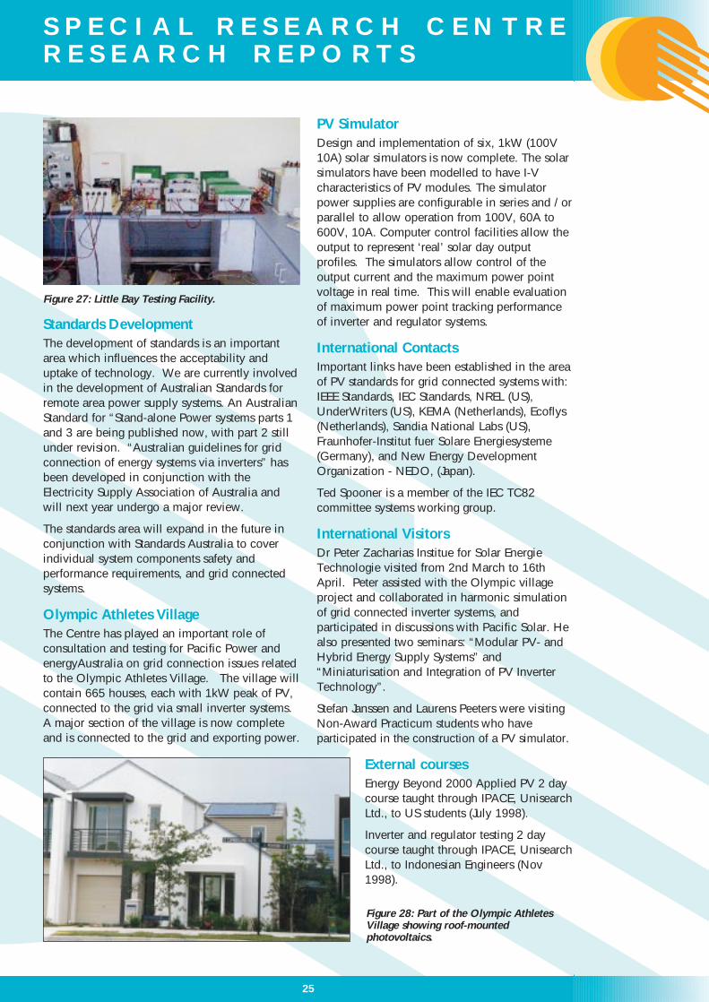
Figure 27: Little Bay Testing Facility.
Standards DevelopmentThe development of standards is an importantarea which influences the acceptability anduptake of technology. We are currently involvedin the development of Australian Standards forremote area power supply systems. An AustralianStandard for “Stand-alone Power systems parts 1and 3 are being published now, with part 2 stillunder revision. “Australian guidelines for gridconnection of energy systems via inverters” hasbeen developed in conjunction with theElectricity Supply Association of Australia andwill next year undergo a major review.
The standards area will expand in the future inconjunction with Standards Australia to coverindividual system components safety andperformance requirements, and grid connectedsystems.
Olympic Athletes VillageThe Centre has played an important role ofconsultation and testing for Pacific Power andenergyAustralia on grid connection issues relatedto the Olympic Athletes Village. The village willcontain 665 houses, each with 1kW peak of PV,connected to the grid via small inverter systems.A major section of the village is now completeand is connected to the grid and exporting power.
Figure 28: Part of the Olympic AthletesVillage showing roof-mountedphotovoltaics.
PV SimulatorDesign and implementation of six, 1kW (100V10A) solar simulators is now complete. The solarsimulators have been modelled to have I-Vcharacteristics of PV modules. The simulatorpower supplies are configurable in series and / orparallel to allow operation from 100V, 60A to600V, 10A. Computer control facilities allow theoutput to represent ‘real’ solar day outputprofiles. The simulators allow control of theoutput current and the maximum power pointvoltage in real time. This will enable evaluationof maximum power point tracking performanceof inverter and regulator systems.
International ContactsImportant links have been established in the areaof PV standards for grid connected systems with:IEEE Standards, IEC Standards, NREL (US),UnderWriters (US), KEMA (Netherlands), Ecoflys(Netherlands), Sandia National Labs (US),Fraunhofer-Institut fuer Solare Energiesysteme(Germany), and New Energy DevelopmentOrganization - NEDO, (Japan).
Ted Spooner is a member of the IEC TC82committee systems working group.
International VisitorsDr Peter Zacharias Institue for Solar EnergieTechnologie visited from 2nd March to 16thApril. Peter assisted with the Olympic villageproject and collaborated in harmonic simulationof grid connected inverter systems, andparticipated in discussions with Pacific Solar. Healso presented two seminars: “Modular PV- andHybrid Energy Supply Systems” and“Miniaturisation and Integration of PV InverterTechnology”.
Stefan Janssen and Laurens Peeters were visitingNon-Award Practicum students who haveparticipated in the construction of a PV simulator.
External coursesEnergy Beyond 2000 Applied PV 2 daycourse taught through IPACE, UnisearchLtd., to US students (July 1998).
Inverter and regulator testing 2 daycourse taught through IPACE, UnisearchLtd., to Indonesian Engineers (Nov1998).

Education andExternal ActivitiesUniversity Staff:Robert Largent, David Roche, Dr ChristianaHonsberg, Paul Rowley
Australian Short CoursesShort courses in energy efficiency and renewableenergy for building companies, school andcommunity workshops and local governmentforums have all contributed to a successfulportfolio of education and training programs atthe Centre. These programs are supported bystrong research foundations; currently, projectsinvolving energy management and policydevelopment, along with technological aspects ofrenewable energy generation are in progress atthe Centre.
Education and training activities have alsoinvolved cooperative project development with anumber of State and Commonwealth bodies,such as the Sustainable Energy DevelopmentAuthority and the Australian CRC for RenewableEnergy (ACRE). Additionally, the Centre’seducation and training facility has won a numberof consultancy contracts. These includedevelopment of SEDA’s Energy Smart HomesTraining program and short course provision forindustry groups.
Internet and CD based Course MaterialsThe Centre is at the leading edge of programdelivery technology - its work in developingInternet and World Wide Web-based educationprograms and learning networks has gainedinternational recognition, including theinvolvement of the BBC On-line in itsdevelopment.
An internet based “Applied PV”course was run in1998, in conjunction with ACRE for 35 studentsworldwide. Course material was supplied viaCD-Rom and tutoring via internet. Six studentssubsequently undertook an in-housesupplementary course, allowing hands-onlaboratory and computing work. The course willbe offered again in 1999.
Work continues on CD-ROM teaching materials,initially based on the Centre’s AppliedPhotovoltaics undergraduate course. The aim isto be able to use the CDs at different levels,catering for high school, undergraduate andpostgraduate PV courses.
26
E D U C A T I O N A N D E X T
International Short CoursesThe PVSRC conducted a three week intensivecourse in Applied Photovoltaics for high levelengineers and policy makers of Indonesia’s BPPT.BPPT is currently finishing off the installation of38,000 domestic home lighting systems inremote areas of Indonesia. Each system consistsof a 50 watt Solarex PV module, a lead acidbattery and three fluorescent lights. Provisionsare also made to power a radio and a smalltelevision. BPPT reports that plans are beingmade to expand the project to 1,000,000 PVlighting systems for remote areas.
Figure 29: Dr. Honsberg and Dr. Cotter withIndonesia’s BPPT.
Figure 30: BPPT Engineers in Water Pumping Tutorial
Figure 31: BPPT in Applied Photovoltaics Tutorial.

High School EducationRooftop PV arrays for schools have significanteducational value. As well as being responsiblefor the technology (such as the 1kW array on FortSt High School in NSW), the PVSRC is workingon an ACRE Solar Schools project with MurdochUniversity and the Australian NationalUniversity, with the aim of developing aneducational program for teachers and students.Educational groups have also taken advantage of
Centre expertisewith special lecturesinvolving electricitydemonstrations tohigh schoolstudents. Theselectures have provedto be very popularwith the SiemensScience Experienceand the giftedchildren groups andhelp teach basicelectricity conceptsto buddingengineers andscientists.
27
Figure 34: ACRE Funded Solar Viewing Telescopewith Cranbrook Students.
Photovoltaics for Non-EngineersThis year a new course was offered at UNSWspecifically designed for teaching photovoltaicsto non-engineering based students. The coursewas taught through the general education systemand only non-engineering students were eligibleto enrol. Photovoltaics concepts were taughtthrough the study of the 1996 World SolarChallenge with subjects as follows:Aerodynamics, solar arrays, motors, motorcontrollers, batteries, suspension, brakes andwheels. The students designed, built and racedmodel solar cars constructed of recycledmaterials utilising the concepts learned duringthe course. The race itself was a striking eventwith several hundred university studentsattending.
E R N A L A C T I V I T I E S
Figure 32: Fort St. HighSchool with 1kW PV systemvisible on roof.
Figure 33: Dr. Jeff Cotter demonstrating for giftedchildren seminar.
Renewable Energy LecturesThe PVSRC provides lectures on renewableenergy to High Schools thus helping to promotethe understanding of renewable energy. TheCooperative Research Centre for RenewableEnergy (ACRE) has provided funding forequipment used in these lectures. Figure 35: Model Solar Car designed by Non-
Engineering Students.

Industrial DesignThe PVSRC assists Industrial Design studentsfrom UNSW and the University of Sydney in finalyear projects. The design criteria used byIndustrial Design is tailored to sound engineeringprinciples. The PV module’s physical size, thebattery dimensions and mass, the energy storagerequirements and energy control are allevaluated and, over a period of months, thestudent’s effort form the project into a PVproduct.
28
E D U C A T I O N A N D E X T
Figure 36: Industrial Design Student Marcel Julliard’sPV Lantern and Portable Power Supply.
Figure 37: Industrial Design Student Marcel Julliard’sPV Lantern Ready for Charge.
UNSW Courses and Careers Day andFaculty of Engineering Open Day.This year UNSW Courses and Careers Day washeld on 5th September, allegedly the month oflowest annual rainfall in Sydney and, similarly tolast year, it rained. Fortunately, rain did notdampen the enthusiasm of those prospectivestudents lining up to learn about photovoltaics,land the interactive solar powered modelhelicopter and receive their “free orange juice”squeezed by Centre volunteers on solar poweredjuicers. Over 10,000 prospective students visitedUNSW with many flocking to the Engineeringfaculty with its interactive displays. The displays,designed by Gordon Bates, were supplementedwith career advice from senior academics and alecture by the Centre’s External RelationsManager, Rob Largent, entitled “Clean, Green &Cost Effective: Electrical Engineering designingNew Solar Energy Systems”.
Figure 38: Prospective students and friends queue atthe Centre display, Courses and Careers Day 98.
Figure 39: Perfect touchdown for the interactive solarpowered model helicopter.
29
Figure 40: Centre Display at ERDIC Annual Seminar.
E R N A L A C T I V I T I E S
External RelationsManagers:Robert Largent, David Roche
Project Staff: Linda Koschier, Donald Clugston, Matt Borland
A high level of public and media interest in theCentre was maintained throughout 1998. Thisinterest was met through the usual channels ofphone and e-mail correspondence, printedinformation sheets, laboratory tours, exhibitiondisplays, open days, media liaison and theCentre’s world-wide web site.
The Centre’s information sheets were updatedand expanded to cover additional topics. Theseinformation sheets form a core aspect of theCentre’s external relations, since they provide awealth of information on photovoltaics and theCentre’s work in a readily available and easilyunderstood format. These information sheets areaccessible on the Centre’s world-wide web site“http://www.pv.unsw.edu.au/info/”.
Numerous national and regional radio interviewswere conducted throughout the year on topicsranging from energy efficiency to solar cars.
The Centre’s work or staff appeared in a numberof publicationsincluding theSydney MorningHerald, theMelbourne Age,Geo Magazine,Australian EnergyNews and Uniken.
Figure 41: Prof.Martin Green onthe cover ofAustralian EnergyNews.
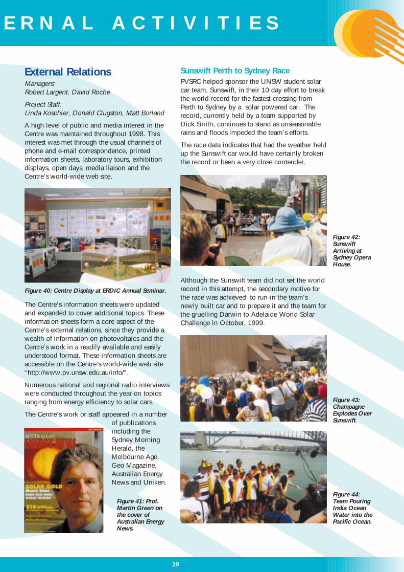
Sunswift Perth to Sydney RacePVSRC helped sponsor the UNSW student solarcar team, Sunswift, in their 10 day effort to breakthe world record for the fastest crossing fromPerth to Sydney by a solar powered car. Therecord, currently held by a team supported byDick Smith, continues to stand as unseasonablerains and floods impeded the team’s efforts.
The race data indicates that had the weather heldup the Sunswift car would have certainly brokenthe record or been a very close contender.
Although the Sunswift team did not set the worldrecord in this attempt, the secondary motive forthe race was achieved: to run-in the team’snewly built car and to prepare it and the team forthe gruelling Darwin to Adelaide World SolarChallenge in October, 1999.
Figure 43:ChampagneExplodes OverSunswift.
Figure 44:Team PouringIndia OceanWater into thePacific Ocean.
Figure 42:SunswiftArriving atSydney OperaHouse.

Stand Alone Power Supply SystemsThe Centre’s expertise in applied photovoltaicshas been effectively put to use by the NationalParks and Wildlife Service (NPWS).
The success of the NPWS Montague IslandPV/diesel hybrid system installed in 1997 hasprompted NPWS to install a 6 kW PV/dieselhybrid system at Green Cape on the far southcoast of NSW. This system is due forcommissioning in early 1999.
Ongoing data analysis from the Montague Islandhybrid system has shown that the diesel requiredto power the island has been reduced by over80%. NPWS has reported that the PV/dieselhybrid system will pay for itself in only eightyears based solely upon the per litre cost ofdiesel. If NPWS also takes into account the costsassociated with the transport of the diesel to theisland the system will pay for itself much sooner.
Montague Island is an ecologically sensitive areawith Australia’s only year round seal colony andpenguin rookeries. NPWS desired both to reducethe ecological risk of a diesel spill and reduce thefinancial burden of supplying fossil fuel forelectricity generation.
30
E D U C A T I O N A N D E X T
Figure 45: Montague Island: 4 kWp PV Array used topower island community.
Design Assistance DivisionManager: Robert Largent
University Staff: Dr Christiana Honsberg
Project Staff: David Roche
The Centre’s Design Assistance Division (DAD)has a primary function to make available theCentre’s photovoltaic and systems expertise toUniversity and off-campus individuals andgroups.
The DAD handles public enquiries regarding thetechnical issues concerning PV and its associatedequipment by offering information, advice andcommercial contacts. Advice ranges from RAPSinformation, equipment suppliers, and systemsizing to recommending the best locations ingardens to install solar powered lights.
Technical support for industry is diverse, rangingfrom enquiries concerning commerciallyavailable solar technology to instituting fullprojects for the development (to the pre-commercial stage) of specialised equipment forsolar PV applications.
Notable users of the Centre’s DAD have been:
• ECO Design Foundation• General Technology• Taronga Zoo• National Parks and Wildlife Service• Harry Seidler and Associates• Barry Webb and Associates• energyAustralia• Olympic Organising Committee• Federal Ministry of Health, India• Kenhill Engineers Pty Ltd• Manly Council• The Robinson Group• Taylor Woodrow (Australia) Pty Ltd
As with Montague Island, in the Green Capeproject the PVSRC was chosen for its non-partisan expertise in renewable energy systems.The DAD evaluated the community’s powerrequirements, set tender specifications,conducted a technical site visit for tenderers, andclarified the technical content of the tendersduring tender evaluation thus allowing NPWS tomake informed an decision.
This site is similar to Montague Island with a lighthouse and two cottages. The PV/diesel hybridsystem will supply power for up to 20 people.

31
LightingIndustrial consulting and research (throughUnisearch Ltd) has resulted in a DAD designed2.54 MHz inverter used to power Philipsinduction lamps and a high efficiency MaximumPower Point Tracker designed specifically for BPSolar’s BP 585F (Buried Contact) PV module.This fully dimmable lighting system has a bulblife of fifteen years.
A pre-commercial lighting system using thistechnology has been installed at Gate 9 of theUNSW Kensington campus.
Figure 46: High Efficiency, Fully Dimmable LightingSystem.
PV in BuildingsA growing level of technical support is beingsought by architectural firms for projects bothwithin and outside of Australia. Collaborativeeffort involving Solarch and the DAD is helpingto meet this demand.
Photovoltaics and SculptureArtist Allan Giddy’s sculpture ICE HEART was agreat success during its showing on TamaramaBeach during the Sydney Organising Committeefor the Olympic Games’ Sculpture by the Sea
Figure 48: The Sculpture ICE HEART at TamaramaBeach.
Figure 47: Sculpture Allan Giddy Inserting Ice Heart.
Reflection AnalysisThe DAD offers reflection analysis for proposedPV arrays. In some cases, it is necessary todetermine in advance the intensity of reflection,the times of day and the directions that will beaffected by reflections from PV arrays. Thesereflections can be of concern in both city andrural areas and in both cases small adjustmentsto the orientation or tilt of the array may be ableto minimise the effects of these reflections.
exhibition. The artwork used four buried contactsolar modules on loan from BP Solar to power arefrigeration system which kept an anatomicallymodelled piece of ice shaped as a human hearton display.
The DAD aided in the design of the refrigerationand energy systems for the artwork.
E R N A L A C T I V I T I E S

BackgroundRecognizing the rapid growth of thephotovoltaics industry and its need for trainedstaff, a Key Centre for Teaching and Research inPhotovoltaic Engineering was awarded to theUniversity, commencing in early 1999. This KeyCentre will offer the world’s first undergraduateprogram in Photovoltaics and Solar Energy,beginning in the year 2000. Professor StuartWenham resigned from Associate Directorship ofthe Special Research Centre at the end of 1998 totake on the role of Director of the Key Centre.As detailed in Professor Wenham’s report at thefront of this volume and further below, the KeyCentre will initiate strong new programs,particularly in the undergraduate andpostgraduate teaching areas and in industry-initiated research.
The following sections outline the initial industry-linked research projects being undertaken by theKey Centre and gives a detailed outline of thenew undergraduate program leading to thedegree of Bachelor of Engineering inPhotovoltaics and Solar Energy.
Commercial Research
Project with BP SolarBP Solar, one of several licensees of the BCSCtechnology, presently manufactures the highestperforming commercial cells using the standardBCSC process with cell efficiencies in the vicinityof 17%. The aim of this new collaborativeproject negotiated with BP Solar is to developand implement a new solar cell rear structurethat appears to solve the primary limitation of allcurrent commercial solar cells - poorlypassivated rear surfaces. To aid in thecommercial implementation of the UNSW
32
K E Y C E N T R E F O R P H O TE N G I N E E R I N G R E P O R T S
patented designs, funding has been successfullysought by BP Solar from the European Union’sJOULE program. The expected outcome will bethe achievement of significantly higherefficiencies approaching 20% for the BCSCtechnology using solar grade materials, whilesimultaneously lowering costs.
A novel approach for contact formation is tomake use of selective solid phase epitaxial (SSPE)growth. The aluminium (Al) mediated SPEgrowth process is extraordinary in terms of thenature of the growth process, requiredtemperature, quality of crystal grown, ability totolerate interfacial oxide, simplicity and potentialfor low cost. A crystalline silicon surface coatedby a layer of Al and then a layer of sputteredamorphous silicon (a-Si), when heated to 500˚C(below the Al-Si eutectic temperature), leads tothe SPE growth of Al doped silicon onto theadjacent silicon surface. The a-Si penetrates intothe Al (in which it has high mobility andsolubility) to reduce its free energy, followingwhich epitaxial growth takes place at thecrystalline surface as the free energy of the Siatoms is further reduced. A concentrationgradient of Si within the Al results, leading tocontinual diffusion of Si from the a-Si interface tothe crystalline silicon surface where it epitaxiallygrows, doped with Al at its solid solubility.Consequently, the juxtaposed Si and Al layerschange place with the a-Si being converted tocrystalline silicon.
For implementation into the BCSC process, thefront surface is fabricated in the usual way.Continuous (Figure 50(b)) or intermittent (Figure50(a)) grooves can be formed in a grid pattern onthe rear surface by a number of techniques.Damage created by this process may requireetching as is normally the case with front groovesfor the BCSC. The SSPE growth process is thenimplemented and should facilitate SPE growth ofp+ silicon onto the exposed substrate p-typeregion following the automatic reduction orremoval of the native oxide. Regions with thickoxide should remain unaffected as demonstratedby preliminary work in Figure 51 where a3,000Å thick oxide layer provided protection forthe crystalline Si surface from the overlying layersof Al and Si. The exposed Al following the SPEgrowth appears well suited to standardelectroless metal plating used for conventionalBCSC devices. UNSW owns the correspondingintellectual property and has already negotiatedrights with BP Solar.
Figure 49:UNSWCommercialTechnologyproduced by BPSolar, held byits inventorsMartin Green(left) and StuartWenham.
PHOTO BY STUART DAVIDSON
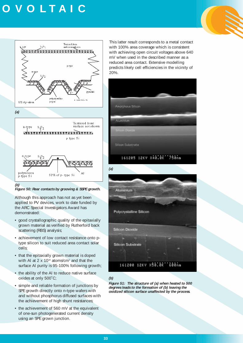
Although this approach has not as yet beenapplied to PV devices, work to date funded bythe ARC Special Investigators Award hasdemonstrated:
• good crystallographic quality of the epitaxiallygrown material as verified by Rutherford backscattering (RBS) analysis;
• achievement of low contact resistance onto p-type silicon to suit reduced area contact solarcells;
• that the epitaxially grown material is dopedwith Al at 2 x 10¹⁸ atoms/cm3 and that thesurface Al purity is 95-100% following growth;
• the ability of the Al to reduce native surfaceoxides at only 500˚C;
• simple and reliable formation of junctions bySPE growth directly onto n-type wafers withand without phosphorus diffused surfaces withthe achievement of high shunt resistances;
• the achievement of 560 mV at the equivalentof one-sun photogenerated current densityusing an SPE grown junction.
33
This latter result corresponds to a metal contactwith 100% area coverage which is consistentwith achieving open circuit voltages above 640mV when used in the described manner as areduced area contact. Extensive modellingpredicts likely cell efficiencies in the vicinity of20%.
(a)
(b)Figure 50: Rear contacts by grooving & SSPE growth.
(a)
(b)Figure 51: The structure of (a) when heated to 500degrees leads to the formation of (b) leaving theoxidized silicon surface unaffected by the process.
O V O L T A I C

Project with Eurosolare, ItalyA collaborative research plan has been agreedupon with Eurosolare addressing majoradaptation of the BCSC fabrication to suit existingscreen-printing equipment/infrastructure. Newintellectual property to suit these requirementshas been recently generated at UNSW. Alicensing agreement is being negotiated withincentives for Australian manufacture. A furtherchallenge for the collaborative research is todevelop processes compatible with constraintsimposed by Eurosolare’s polycrystalline siliconsubstrates. A three year program has been agreedupon, including exchange of researchers(including a UNSW PhD student) betweenUNSW and Eurosolare. A technology transfer toEurosolare is planned during 1999.
Project with Pacific SolarPacific Solar has already purchased the rights toUNSW thin-film technology. Collaborativeresearch will focus on improving the siliconmaterial quality by capitalizing on state-of-the-artcharacterization equipment available at PacificSolar in conjunction with the high level ofexpertise available through the Key Centre. Adetailed research plan has been agreed uponwith the involvement of 3 PhD studentsanticipated.
Grid-connected PV ProjectsThese projects focus on grid-connected issues forPV such as system design, grid dynamics,impedance matching, harmonics, long lifeinverter design, transmission line voltagedistribution, etc. as well as more general systemhardware issues. Emphasis will also be placedon broader institutional/policy and environmentalissues and the restructuring of the electricityindustry. The scope of the correspondingprogram will be expanded where appropriateinto related areas of research to generateadditional knowledge for the teaching program.To date, one project has been negotiated with,and will be funded by, Pacific Solar relatingspecifically to grid-connected inverters.
Space Cells Project with UnisearchCells for space applications vary significantlyfrom terrestrial cells with greater importanceplaced on performance and tolerance toradiation damage from the harsh spaceenvironment. UNSW high efficiency solar cellsmay be prime candidates for space where apremium can be paid for their unique attributes.
34
K E Y C E N T R E F O R P H O TE N G I N E E R I N G R E P O R T S
Device reliability, performance at “end-of-life”,suitability for the environment, radiation hardnessand thermal design are some of the issues to beaddressed by this research strand. Funding toestablish and operate a pilot production facilityhas already been granted by UNSW with futurework expected to be self-supporting. The futureof this work (in the context of the Key Centre)will depend on the industry’s interest in highperformance silicon solar cells for space use.
TeachingOverview of course 3642 inPhotovoltaics and Solar EnergyThe undergraduate engineering degree programin Photovoltaics and Solar Energy is to beestablished in the year 2000 in response to rapidgrowth in the industry in both manufacturingcapacity and job creation. Course materialscover all aspects of photovoltaic engineeringincluding: research, development, education andtraining; photovoltaic technology, manufacturing,quality control and product reliability;photovoltaic applications, system design,performance optimisation, system integration,balance of system components includinginterface and control electronics, grid interfaceissues, system analysis, fault diagnosis andreliability; device theory and design; marketing,analysis, life cycle costing, modelling and policy;and a broad education in solar energy,renewable energy technologies and sustainableenergy. All areas are covered briefly in the firsttwo years while in the 3rd and 4th years, scopeexists for specialising in preferred areas.Throughout the course, considerable emphasis isplaced on gaining hands-on experience ofworking with photovoltaic devices, modules andsystems, such as through the solar car projectand solar powered houses, such as in theOlympic village.
A unique feature of the degree is that students aregiven the opportunity to also specialise in acomplementary area, such as one of the otherengineering disciplines. In 2nd year, students areable to enrol in one 18 Credit Point strandchosen from the areas of computing, electronics,telecommunications, chemistry, mathematics,environmental/civil engineering, electric energyand mechanical engineering. The chosen strandwill provide the necessary core material tofacilitate subsequent selection of more advancedelectives from the corresponding area in the 3rdand 4th years of the Photovoltaics and Solar

Energy degree. This may make it feasiblethrough an extra 5th year of study to achieve adouble degree such as in Photovoltaics and SolarEnergy combined with say Electrical Engineering.It may also be possible for students with analternative engineering degree to also gain adegree in Photovoltaics and Solar Energy througha 5th year of study.
35
Course OutlineThe following is the course outline to be printed in the Faculty Handbook pending finalapproval from The University of New South Wales.
YEAR 1 HPW HPWS1 S2 CP
SOLA1050 Introduction to Solar Energy and Photovoltaics 4 3 9CHEM1806 Chemistry 1EE 0 3 3
ELEC1011 Electrical Engineering 1 6 0 6ELEC1041 Digital Circuits 0 4 6
MATH1141 Higher Mathematics 1A 6 0 6MATH1241 Higher Mathematics 1B 0 6 6PHYS1969 Physics 1 6 6 12
Total 22 22 48
MATH1141 and MATH1241 may be taken at the ordinary level.
YEARS 2 & 3 STRAND OPTIONS
Students have the opportunity to select one of eight possible strands to complementtheir education in Solar Energy and Photovoltaic Engineering. Each strand comprises 18Credit Points with the opportunity to subsequently select additional Electives in thecorresponding area in the final two years. The eight strands available are listed belowwith the subject(s) comprising the last 6 Credit Points to be taken in year 3.
YEAR 2 HPW HPWS1 S2 CP
Selected Strand 5 5 12
SOLA2051 Project in Photovoltaics and Solar Energy 3 2 6SOLA2020 Photovoltaic Technology and Manufacturing 4 0 6ELEC2042 Real Time Instrumentation 0 4 6MATH2849 Statistics EE 0 3 3MATH2589 Linear Algebra 0 3 3SOLA2050 Sustainable Energy 2.5 0 3SOLA2060 Introduction to Electronic Devices 0 2.5 3
General Education Electives 4 0 6
Total 18.5 19.5 48
O V O L T A I C

36
K E Y C E N T R E F O R P H O TE N G I N E E R I N G R E P O R T S
YEAR 3 HPW HPWS1 S2 CP
Professional Electives 5 10 18Selected Strand (continued) 5 0 6
SOLA3055 Renewable Energy Engineering 2.5 0 3SOLA3540 Applied Photovoltaics 4 0 6SOLA3507 Solar Cells and Systems 0 4 6SOLA3054 Renewable Energy Product Reliability 2.5 0 3
General Education 0 4 6Total 19 18 48
YEAR 4 HPW HPWS1 S2 CP
Professional Electives 5 5 12ELEC4010 Introduction to Management for
Electrical Engineers 4 0 6ELEC4011 Ethics and Electrical Engineering Practice 0 2 3SOLA4012 Grid Connected Photovoltaic Systems 4 0 6SOLA4013 Current Issues in Photovoltaics 0 2.5 3ELEC4903 Industrial Training 0 0 0SOLA4910 Thesis Part A 5 0 6SOLA4911 Thesis Part B 0 10 12
Total 18 19.5 48
YEARS 2 & 3 STRAND OPTIONSStrand 1 Computing and Control HPW HPW
S1 S2 CPCOMP1011 Computing 1A 0 6 6COMP1021 Computing 1B 6 0 6ELEC2041 Microprocessors and Interfacing 4 0 6Strand 2 Electronics HPW HPW
S1 S2 CPELEC2031 Circuits and Systems 3 3 6ELEC3006 Electronics A 6 0 6ELEC3016 Electronics B 0 5 6orELEC3017 Electrical Engineering Design 0 5 6Strand 3 Electric Energy HPW HPW
S1 S2 CPMATH2011 Several Variable Calculus 4 0 6PHYS2939 Electromagnetism 3 0 3ELEC2015 Electromagnetic Applications 0 3 3ELEC3005 Electrical Energy 1 0 5 6Strand 4 Communications HPW HPW
S1 S2 CPELEC2031 Circuits and Systems 3 3 6MATH2620 Complex Analysis 0 2.5 3MATH3150 Transform Methods 0 3 3TELE3013 Telecommunications Systems 1 5 0 6
37
Strand 5 Mathematics HPW HPWS1 S2 CP
MATH2011 Several Variable Calculus 4 0 6MATH2620 Complex Analysis 0 2.5 3MATH1090 Discrete Mathematics 0 3 3MATH3141 Mathematical Methods EE 0 4 6
Strand 6 Mechanical Engineering HPW HPWS1 S2 CP
MECH2700 Thermodynamics 1 2 2 5MECH2600 Fluid Dynamics 1 2 2 5MECH3702 Heat Transfer 0 2 2MECH4720 Solar Energy 3 or 3 3MECH4740 Thermal Power Plants 3 or 3 3
Strand 7 Civil Engineering HPW HPWS1 S2 CP
CIVL1312 Statics 3 0 3CIVL1314 Mechanics of Solids 0 3 3CIVL2314 Engineering Materials 2 3 5CIVL2312 Introduction to Structures 2 0 3CIVL3116 Engineering Management 1 2 2 4
Strand 8 Chemical Engineering HPW HPWS1 S2 CP
CEIC0010 Mass Transfer and Material Balance 2 2 4INDC3010 Thermodynamics 3 0 3CHEN2030 Heat Transfer 0 3 3CEIC2040 Applied Electrochemical and Surface Processes 1.5 0 2INDC3031 Experimental Design 2 1 3INDC3041 Corrosion in the Chemical Industry 0 3 3
PROFESSIONAL ELECTIVES FOR YEARS 3 & 4 HPW HPWS1 S2 CP
SOLA4508 High Efficiency Silicon Solar Cells 0 2.5 3SOLA4010 Building Integrated Photovoltaics 0 2.5 3SOLA4011 Solar Cells: Operating Principles and Technology 0 4 6SOLA4053 Wind Energy Converters 0 4 6SOLA4052 Biomass 4 0 6SOLA4051 Life Cycle Assessment 2 0 3SOLA4050 Renewable Energy Policy and International Programs 2 0 3
Electives can also be chosen from the subjects listed as electives for ElectricalEngineering, Mechanical Engineering, Civil Engineering, Environmental Engineering,Computer Science and Engineering and Chemical Engineering for which appropriatepre-requisite requirements have been satisfied and which conform to the credit pointrequirements.
O V O L T A I C
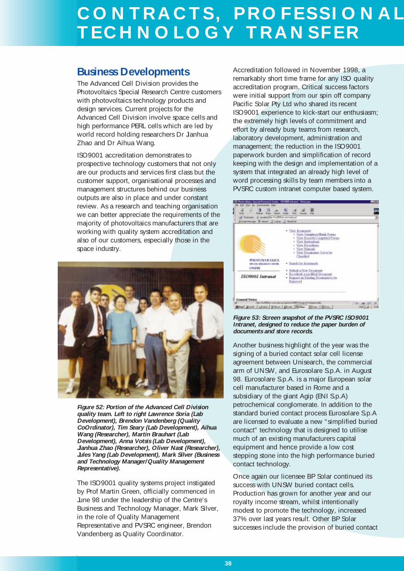
Business DevelopmentsThe Advanced Cell Division provides thePhotovoltaics Special Research Centre customerswith photovoltaics technology products anddesign services. Current projects for theAdvanced Cell Division involve space cells andhigh performance PERL cells which are led byworld record holding researchers Dr JianhuaZhao and Dr Aihua Wang.
ISO9001 accreditation demonstrates toprospective technology customers that not onlyare our products and services first class but thecustomer support, organisational processes andmanagement structures behind our businessoutputs are also in place and under constantreview. As a research and teaching organisationwe can better appreciate the requirements of themajority of photovoltaics manufacturers that areworking with quality system accreditation andalso of our customers, especially those in thespace industry.
38
C O N T R A C T S , P R O F E S S I O N A LT E C H N O L O G Y T R A N S F E R
Figure 52: Portion of the Advanced Cell Divisionquality team. Left to right Lawrence Soria (LabDevelopment), Brendon Vandenberg (QualityCoOrdinator), Tim Seary (Lab Development), AihuaWang (Researcher), Martin Brauhart (LabDevelopment), Anna Votsis (Lab Development),Jianhua Zhao (Researcher), Oliver Nast (Researcher),Jules Yang (Lab Development), Mark Silver (Businessand Technology Manager/Quality ManagementRepresentative).
The ISO9001 quality systems project instigatedby Prof Martin Green, officially commenced inJune 98 under the leadership of the Centre’sBusiness and Technology Manager, Mark Silver,in the role of Quality ManagementRepresentative and PVSRC engineer, BrendonVandenberg as Quality Coordinator.
Figure 53: Screen snapshot of the PVSRC ISO9001Intranet, designed to reduce the paper burden ofdocuments and store records.
Accreditation followed in November 1998, aremarkably short time frame for any ISO qualityaccreditation program. Critical success factorswere initial support from our spin off companyPacific Solar Pty Ltd who shared its recentISO9001 experience to kick-start our enthusiasm;the extremely high levels of commitment andeffort by already busy teams from research,laboratory development, administration andmanagement; the reduction in the ISO9001paperwork burden and simplification of recordkeeping with the design and implementation of asystem that integrated an already high level ofword processing skills by team members into aPVSRC custom intranet computer based system.
Another business highlight of the year was thesigning of a buried contact solar cell licenseagreement between Unisearch, the commercialarm of UNSW, and Eurosolare S.p.A. in August98. Eurosolare S.p.A. is a major European solarcell manufacturer based in Rome and asubsidiary of the giant Agip (ENI S.p.A)petrochemical conglomerate. In addition to thestandard buried contact process Eurosolare S.p.Aare licensed to evaluate a new “simplified buriedcontact” technology that is designed to utilisemuch of an existing manufacturers capitalequipment and hence provide a low coststepping stone into the high performance buriedcontact technology.
Once again our licensee BP Solar continued itssuccess with UNSW buried contact cells.Production has grown for another year and ourroyalty income stream, whilst intentionallymodest to promote the technology, increased37% over last years result. Other BP Solarsuccesses include the provision of buried contact

39
A C T I V I T I E S A N D
solar cells for the grid connected roof top panelsin the new athletes village at the Sydney 2000Olympic site (Figure 28) and the announcementin October 1998 of a new 20-50MWpa buriedcontact production facility to be built at Belrosein Sydney.
In addition to the above activities, the Centrecontinued to provide technical services to thephotovoltaics and electrical utility industry, withnew product testing at its Little Bay SolarResearch Facility, the development of newstandards and guidelines for renewableinterconnection to the supply grid, and variousstudies, courses and seminars in the general areaof renewable energy systems.
Contracts and AgreementsPacific Solar Pty. Ltd. Pacific Solar commenced operation in February,1995 as a $64 million collaborative venturebetween Pacific Power and Unisearch Ltd. Thecompany’s mission is to commercialize themultilayer thin film technology developed by theCentre. The company is leasing the Centre’s BayStreet facility (Figure 54) from the University andis engaging the Centre’s services for contractualresearch. Additionally, a number of Centre staffhave been seconded from the Centre for theduration of the company’s developmental phaseto assist in meeting the company’s objectives.During 1998, Pacific Solar commenced pilotproduction of thin-film polycrystalline silicon-on-glass modules using Centre technology.
energyAustraliaenergyAustralia provided Foundation Sponsorshipfor the Little Bay Solar Energy Research Facility.Their sponsorship includes funding ofphotovoltaic-based power systems installed atthe site. Funding of $85,000 was providedtowards construction of the building in 1994 andanother $240,000 over 3 years towards thephotovoltaic system.
energyAustralia has also been involved in othercollaborative projects with the Centre includingthe Australian High School Project and theAustralian Technology Park photovoltaicinstallation.
Additional activities included performanceassessment of selected crystalline and thin filmsilicon module technologies and electronicinterface hardware.
Sandia National LaboratoriesThe long term association of the Centre withSandia continued into 1998, completing over 11years of very fruitful collaboration. During 1998,Sandia supported the development of advancedsilicon cells by testing some of the best cells andmodules under internationally recognisedstandard reference conditions.
Australian Cooperative Research Centrefor Renewable Energy (ACRE)The University of NSW was a foundationmember of ACRE, when it was established in1997 and is undertaking collaborative research at
the PV Centre and at SOLARCH,the University’s solar architecturegroup.
Projects are variously funded byACRE, UNSW, industry and otherresearch organisations. The PVCentre is currently receivingaround $100,000 per year fromACRE for collaborative work onthree projects in ACRE’sEducation program: energyinformation, short courses andschool & community education;and 2 projects in the SystemsIntegration program: standards forPV systems and evaluation ofremote area power supplyoptions.Figure 54: Pacific Solar’s premises at Bay St., Botany.

40
C O N T R A C T S , P R O F E S S I O N A LT E C H N O L O G Y T R A N S F E R
Other Research Contracts and Grants Individual researchers affiliated with the Centreattracted additional grants from other bodies suchas the New South Wales Department of Energy,Environment Australia, the NSW SustainableEnergy Development Authority, and TheAustralian PV Power Systems Consortium.
Licensing AgreementsCompanies now on public record as beinglicensed to use technology developed at theCentre (or assigned Centre intellectual property)include:
BP Solar Australia Pty. Ltd. BP Solar Espana S.A. Central Electronics Ltd., India Eurosolare S.p.A, Italy.Pacific Solar Pty. Ltd.Samsung Electronics Co. Ltd. Solarex Corporation Solarex Pty. Ltd.
Figure 55: Prof. Martin Green and photovoltaic andoptoelectronic postgraduate students of theUniversity of Havana, Cuba.
ConferencesStaff or students affiliated with the Centrepresented papers relevant to photovoltaics at thefollowing local and international conferencesduring the year:
• 2nd World Conference and Exhibition onPhotovoltaic Solar Energy Conversion, Vienna,July, 1998;
• 3rd Biennial Engineering Mathematics andApplications Conference, Adelaide, July, 1998;
• 36th Annual Conference of the Australian andNew Zealand Solar Energy Society (ANZSES),Christchurch, November, 1998;
• II Workshop on Optoelectronic Materials andtheir Application, including Solar Cells, Cuba,November,1998;
• ESAA - 4th Renewable Energy Technologies &Remote Area Power Supplies Conference,Hobart, February, 1998;
• Space Power Satellite Session on the 49thInternational Astronuatical Congress,September, Melbourne, 1998;
• World Ceramics Congress & Forum on NewMaterials, Florence, June 1998.

41
Technology TransferThe main objective of the technology transfergroup is to facilitate the transfer of celltechnology from the Centre’s research laboratoryto companies which license the technology. Thetechnology transfer group bridges the gapbetween the small-scale solar cell processes usedin research work, and the large-scale productionused in industry. This is done by establishingcandidate sequences on the Centre’s pilotproduction line, thereby demonstrating thesuitability of the technology to commercialisationand providing a training ground for the Centre’slicensees.
The technology transfer group works closely withUnisearch Ltd, the commercial arm of theUniversity of New South Wales. Whentransferring technology to a licensee, its activitiesmay be divided into two main sections:
Cell-Processing Training.This includes the following:
• The preparation of a document outlining thescientific and engineering principles underlyingthe design, fabrication, operation andcommercialisation of the new technology;
• The provision of a series of seminars on variousaspects of the new technology;
• The provision of practical training for licenseepersonnel in all aspects of the production ofthe new photovoltaic devices. The training iscarried out at the Centre’s pilot productionfacility. The trainees are provided with detaileddocumentation of the processing sequence.They observe and participate in the day-to-dayoperation of the pilot production facility. Thelevel of training is such that the trainees are ina position to fabricate devices with minimalassistance from Centre staff;
• Technology transfer visits are organised atappropriate stages of the development of thelicensee’s own pilot production facility. Duringthese visits, one or more research engineersfrom the Centre visit the licensee’s facilities fora period of approximately one week. The mainpurpose of these visits is to get first handexperience of any problems which may arise,to suggest solutions to these problems, and toestablish a strong communication link betweenkey technical personnel;
• The Centre’s research engineers makethemselves available to offer the licenseesprompt and specific technical assistance byfacsimile or telephone, if the need arises.
Advising on Equipment.The Centre provides technical support andadvice to licensees as they establish their ownlaboratories and pilot production facilities. Thedegree of the Centre’s involvement may includeall or any part of the full spectrum of systemintegration:
• Cost analyses;
• Feasibility studies;
• Planning;
• Design of equipment (where appropriate);
• Acquisition of equipment and materials(technical specifications, quotations, freight);
• Installation and commissioning of equipmentand plant;
• Implementation and optimisation of theproduction process.
A C T I V I T I E S A N D

42
F I N A N C E S
PHOTOVOLTAIC SPECIAL RESEARCHCENTRE FINANCESThe Photovoltaics Special Research Centre wasestablished in 1990 with broadly based fundingreceived under the Australian Research Council’s(ARC) Special Research Centres Scheme andfrom Pacific Power. Under the approvedprogram, the Special Research Centre funding isused to provide infrastructure for Centreoperations, seeding funds to bring projects to thestage where they can attract externalsupport and complementary funds toimprove the viability and scope ofexternally supported projects. Inaddition to this broadly basedfunding, individual researchers withinthe Centre receive research grantsand contracts for specific projectswithin the Centre’s general area ofinterest.
Total expenditure during 1998 was$3.1 million, with a breakdown ofexpenditure by source of incomeshown in Figure 56.
Figure 56: Breakdown of expenditure by source ofexternal income (total expenditure is $3.1million).
Only 28% of total expenditure wasfrom income from the ARC SpecialResearch Centres scheme, meetingthe Centre’s target of 45% or less forthis figure. Another substantialsource of funds was Pacific Solar,with large funding totals alsoreceived for specific projectsproposed by researchers affiliatedwith the Centre supported by theAustralian Research Council’s grants
and fellowship schemes. Significant amountswere received from the Australian Co-operativeResearch Centre in Renewable Energy andGreenhouse Gas Abatement (ACRE), and avariety of other sources. The Centre alsoreceived considerable support from theUniversity in the form of infrastructural supportgrants and a major capital grant. The Universityalso provided other substantial non-cash supportto the Centre.
Figure 57: Overall expenditure by category (totalexpenditure is $3.1million).
The chart above (Figure 57) shows the broadareas where funds were spent. Salariesaccounted for close to 50% of expenditure. TheCentre has a target for 1999 of reducingexpenditure to 40% on salaries. Figure 57 alsoshows the progressively smaller percentagesspent on equipment, materials and travel.
Figure 58 shows the corresponding breakdownfor the expenditure of the specific funds receivedunder the ARC Special Research Centres Scheme.These funds have a special role in maintainingand developing the Centre infrastructure.
Figure 58: Expenditure by category of ARC SpecialResearch Centre funds (total of expenditure shown is$887,491).

43
A breakdown of total Centre expenditure byproject area is shown in Figure 59. Thisexpenditure, as in the early years of the Centre,was weighted heavily towards near-term bulkdevice research. This primarily reflected thesuccess in obtaining external funding for specificresearch projects in this area, including a largecapital grant during 1998.
With the maturing of the thin film device work,appreciable external funding is now beingreceived for this area so that it now approachesthe level of support for bulk device work.Although a smaller component of totalexpenditure, external funding for the expandingactivities in the systems area is also becomingsignificant. The figures shown do not accuratelyreflect total Centre effort directed to the areasindicated, since University resources directed tothese areas by way of salary, space and otherinfrastructural support are not included.
Figure 59: Breakdown of total Centre expenditure byproject area (total expenditure is $3.1million).
Finally, Figure 60 shows the breakdown ofexpenditure by project area of broadly basedfunding received by the Centre from the ARCSpecial Research Centres Scheme. The ARCfunding has been used primarily to providesupport for the operation, maintenance anddevelopment of Centre laboratories and facilities,with special attention paid to the nurturing ofsystem research activities.
Apart from direct cash funds received and shownin Figure 56, support from the University is notincluded in any of the previous figures. TheUniversity provides salaries for 9 of the academicstaff and 4 of the non-academic staff involvedwith the Centre. The University also providesaccommodation and a range of services for theCentre, as well as infrastructural support by wayof facilities, such as the library.
Figure 60: Breakdown of expenditure by project areaof funding from the ARC Special Research CentresScheme (total of expenditure shown is $887,491).

44
1 9 9 8 P U B L I C A T I O N S
THESISRichards, B.S., “Optical Charaterisation ofSputtered Silicon Thin Films for PhotovoltaicApplications”, The University of New SouthWales, February, 1998.
BOOKS, BOOK CHAPTERSGreen, M.A., “Solar Cells”, in S.M. Sze (eds),Modern Semiconductor Device Physics (Wiley-Interscience Publication), pp.473-530, 1998.
Schäfer, A.I., Basson, L., and Richards, B.S.,“Environmental Engineering Research Event1998”, Conference Proceedings, Published byUNESCO Centre for Membrane Science andTechnology (UNSW) and Department ofChemical Engineering (USyd), December, 1998,ISBN 0 7334 05193.
REFEREED JOURNALSBasore, P.A., “Event Report: Sunrayce 97”,Progress in Photovoltaics: Research andApplications, Vol. 6, No. 1, pp.69-75, 1998.
Corkish, R., “But they’ll never recover the energyit took to make them.....”, Solar Progress, Vol. 19,No. 3, pp. 14-15, September, 1998.
Corkish, R., Puzzer, T., Sproul, A.B., and Luke,K.L., “Quantitative interpretation of electron-beam-induced current grain boundary contrastprofiles, with application to silicon”, Journal ofApplied Physics, Vol. 84, No. 10, pp. 5473-5481, 1998.
Cotter, J.E., “Model of the Optical Intensity ofLight in Silicon Layers with Rear DiffuseReflectors”, Journal of Applied Physics, Vol. 84,No. 1, pp. 618-623, 1998.
Green, M.A., “Comments on 17.3% EfficiencyMetal-Oxide-Semiconductor (MOS) Solar Cellswith Liquid-Phase Deposited Silicon Dioxide”,IEEE Electron Device Letters, Vol. 19, pp. 447-449, 1998.
Green, M.A., “Photovoltaic Solar EnergyConversion: Recent Progress”, Korean Journal ofElectrical and Electronic Material, Vol. 11. Pp.100-105, October, 1998.
Green, M.A., Emery, K., Bücher, K., King, D.L.,and Sanekazu, I., “Solar Cell Efficiency Tables(Version 11)”, Progress in Photovoltaics: Researchand Applications, Vol. 6, No. 1, pp. 35-42, 1998.
Green, M.A., Emery, K., Bücher, K., King, D.L.,and Igari, S., “Solar Cell Efficiency Tables(Version 12)”, Progress in Photovoltaics: Researchand Applications, Vol. 6, pp. 265-270, 1998.
Green, M.A., and Jordan, D., “Technology andEconomics of Three Advanced Silicon SolarCells”, Progress in Photovoltaics: Research andApplications, Vol. 6, No. 3, pp. 169-180, 1998.
Nast, O., Puzzer, T., Koschier, L.M., Sproul, A.B.,and Wenham, S.R., “Aluminium InducedCrystallization of Amorphous Silicon on GlassSubstrates Above and Below the EutecticTemperature”, Applied Physics Letters, Vol. 73,pp. 3214-3216, 1998.
Outhred, H.R., “A Review of Electricity IndustryRestructuring in Australia”, Electric PowerSystems Research, Vol. 44, pp. 15-25, 1998.
Shi, Z., and Green, M.A., “Survey of MaterialOptions and Issues for Thin Film Silicon SolarCells”, Progress in Photovoltaics: Research andApplications, Vol. 6, pp. 247-257, 1998.
Watt, M.E., Johnson, A.J., Ellis, M., and Outhred,H.R., “Life-Cycle Air Emissions from PV PowerSystems”,Progress in Photovoltaics: Research andApplications, Vol. 6, No. 2, pp. 127-136, 1998.
Wenham, S.R, Bowden, S., Dickinson, M.,Largent, R., Shaw, N., Honsberg, C.B., andGreen, M.A., “Low Cost Photovoltaic Roof Tile”,Solar Energy Materials and Solar Cells, Vol. 47,pp. 325-337, October, 1997. (omitted from 1997Annual Report).
Zhang, G., Zhao, J., and Green, M.A., “Effect ofSubstrate Heating on the Adhesion and HumidityResistance of Evaporated MgF2/ZnSAntireflection Coatings and on the Performanceof High Efficiency Silicon Solar Cells”, SolarEnergy Material and Solar Cells, Vol. 51, pp.393-400, 1998.
Zhao, J., Wang, A., Green, M.A., and Ferrazza,F., “19.8% Efficient “Honeycomb” TexturedMulticrystalline and 24.4% MonocrystallineSilicon Solar Cells”, Applied Physics Letters, Vol.73, pp. 1991-1993, 1998.
Zheng, G.F., Zhang, W., Shi, Z., Thorp, D.,Bergmann, R.B., and Green, M.A., “Highefficiency drift-field thin-film silicon solar cellsgrown on electronically inactive substrates”,Solar Energy Materials and Solar Cells, Vol. 51,pp. 95-104, 1998.

45
CONFERENCE PAPERS & REPORTSCorkish, R.P., and Honsberg, C.B., “NumericalModelling Of Quantum Well Solar Cells”, 2ndWorld Conference and Exhibition onPhotovoltaic Solar Energy Conversion, Vienna,July, 1998.
Corkish, R.P., Sproul, A.B., Puzzer, T., Altermatt,P.P., Heiser, G., and Keung, L.L., “QuantitativeAnalysis Of Electron-Beam-Induced-CurrentProfiles Of Grain Boundaries In MultycrystallineSolar Cells”, 2nd World Conference andExhibition on Photovoltaic Solar EnergyConversion, Vienna, July, 1998.
Cotter, J.E., Richards, B.S., Ferrazza, F.,Honsberg, C.B., Leong, T.W., Mehravarz, H.R.,Naik, G.A., and Wenham, S.R., “Design Of ASimplified Emitter Structure For Buried ContactSolar Cells”, 2nd World Conference andExhibition on Photovoltaic Solar EnergyConversion, Vienna, July, 1998.
Färber, G., Bardos, R.A., McIntosh, K.R.,Honsberg, C.B., and Sproul, A.B., “Detection OfShunt Resistance In Silicon Solar Cells UsingLiquid Crystals”, 2nd World Conference andExhibition on Photovoltaic Solar EnergyConversion, Vienna, July, 1998.
Green, M.A., “Excitons In Silicon Solar Cells:Room Temperature Distributions And Flows”,2nd World Conference and Exhibition onPhotovoltaic Solar Energy Conversion, Vienna,July, 1998.
Green, M.A., “Photovoltaic Solar EnergyConversion: An Update”, ATSE Focus, No. 102,May/June, 1998.
Green, M.A., “Photovoltaics: Heading for theSuburbs”, MRS Bulletin, Vol. 23, No. 6, pp. 4-5,1998.
Green, M.A., “Recent Developments inPhotovoltaics”, II Workshop on OptoelectronicMaterials and their Application, including SolarCells, Havana, Cuba, 2-6 November, 1998.
Green, M.A., “Status and Prospects of Devicesand Systems for Photovoltaic Solar EnergyConversion”, CIMTEC Conference, Florence,June, 1998.
Green, M.A., Zhao, J., Wang, A., “23% PVModule And Other Silicon Solar Cell Advances”,2nd World Conference and Exhibition onPhotovoltaic Solar Energy Conversion, Vienna,July, 1998.
Green, M.A., Zhao, J., Wang, A., “RecentAdvances in Silicon Solar Cell Efficiency”,Proceedings of the 36th Annual Conference ofthe Australian and New Zealand Solar EnergySociety, (ANZSES Solar ‘98), 25-27 November,1998, Christchurch, New Zealand, pp. 483-490.
Koschier, L.M., Wenham, S.R., and Green, M.A.,“Efficiency Improvements In Thin Film SiliconSolar Cells Using SI1-xGEx ALLOYS”, 2nd WorldConference and Exhibition on Photovoltaic SolarEnergy Conversion, Vienna, July, 1998.
Koschier, L.M., Wenham, S.R., Gross, M.,Puzzer, T., and Sproul, A.B., “Low TemperatureJunction And Back Surface Field Formation ForPhotovoltaic Devices”, 2nd World Conferenceand Exhibition on Photovoltaic Solar EnergyConversion, Vienna, July, 1998.
Krcho, D., “Kramers-Kronig Relations in FourierTransform Infrared Spectroscopy ofSemiconductors”, 3rd Biennial EngineeringMathematics and Applications Conference,Adelaide, July, 1998.
Krcho, D., “FTIR Spectroscopy for Thin FilmSilicon Solar Cell Characterisation”, 2nd WorldConference and Exhibition on Photovoltaic SolarEnergy Conversion, Vienna, July, 1998.
Krcho, D., “FTIR Spectroscopy of Silicon-BasedThin Films”, Proceedings of the 36th AnnualConference of the Australian and New ZealandSolar Energy Society, (ANZSES Solar ‘98), 25-27November, 1998, Christchurch, New Zealand,pp. 504-509.
MacGill, I.F., and Kaye, R.J., “OperationalInteractions and Potential Synergies BetweenPhotovoltaics and Distributed Energy Storage”,14th European PVSEC, Barcelona, Spain, 30June, 1997. (omitted from 1997 Annual Report).
McIntosh, K.R., “The Implementation ofPhotovoltaic Solar Power in DevelopingCountries”, Proceedings of the EnvironmentalEngineering Research Event, Avoca Beach(NSW), December, 1998, pp. 267-272.
McIntosh, K.R., Honsberg, C.B., and Wenham,S.R., “Shunt Resistance Paths Across a RearFloating Junction Caused by Edge-Isolation”,Proceedings of the 36th Annual Conference ofthe Australian and New Zealand Solar EnergySociety, (ANZSES Solar ‘98), 25-27 November,1998, Christchurch, New Zealand, pp. 518-523.

46
1 9 9 8 P U B L I C A T I O N S
McIntosh, K.R., Honsberg, C.B., and Wenham,S.R., “The Impact Of Rear Illumination OnBifacial Solar Cells With Floating JunctionPassivation”, 2nd World Conference andExhibition on Photovoltaic Solar EnergyConversion, Vienna, July, 1998.
Pritchard, S.C., McIntosh, K.R., Altermatt, P.P.,and Honsberg, C.B., “A Comparison of SingleJunction and Transistor Structure Solar Cells”,Solar ‘97, ANZSES, 1-3 December, 1997,Canberra. (omitted from 1997 Annual Report).
Remmer, D.P., and Kaye, R.J., “The Effects ofRisk on Energy Choices for Fringe of GridConsumers”, 2nd World Conference andExhibition on Photovoltaic Solar EnergyConversion, Vienna, July, 1998.
Richards, B.S., Cotter, J.E., Ferrazza, F.,Honsberg, C.B., and Wenham, S.R., “Loweringthe Cost of Commercial Silicon Solar Cells”,Proceedings of the Environmental EngineeringResearch Event, Avoca Beach (NSW), December,1998, pp. 303-308.
Richards, B.S., Sproul, A.B., and Lambertz, A.,“Optical Characterisation Of Sputtered SiliconThin Films On Glass”, 2nd World Conferenceand Exhibition on Photovoltaic Solar EnergyConversion, Vienna, July, 1998.
Snow, M., Travers, D.L., Prasad, D.K., Jones, P.,and Watt, M., “Building Integrated Photovoltaics(BIPV) - Developing a Modelling Tool for Cities”,Presented at the 36th Annual Conference of theAustralian and New Zealand Solar EnergySociety, (ANZSES Solar ‘98), 25-27 November,1998, Christchurch, New Zealand.
Spooner, E.D. Zacharias P., Morphett, D.,Grunwald, G., and Mackay, J., “Solar OlympicVillage, Design and Testing Experience”, 2ndWorld Conference and Exhibition onPhotovoltaic Solar Energy Conversion, Vienna,July, 1998.
Sproul, A.B., Puzzer, T., and Bergmann, R.B.,“High Resolution EBIC Imaging Of PolycrystallineSilicon Solar Cells”, 2nd World Conference andExhibition on Photovoltaic Solar EnergyConversion, Vienna, July, 1998.
Watt, M., “Assessing the Value of Renewables”,ESAA - 4th Renewable Energy Technologies &Remote Area Power Supplies Conference,Hobart, 23-25 February, 1998.
Watt, M., “Australian Report on PhotovoltaicPower Applications 1996-97”, Report for theAustralian IEA PV Power Systems Consortium.
Watt, M., Ellis, M., and Outhred, H., (1998),“Photovoltaics in Competitive ElectricityMarkets”, IEA PVPS TI 1998 3.
Wenham, S.R., Honsberg, C., and Green, M.A.,“Development and Commercialisation ofCrystalline Silicon Photovoltaic Technology”,Proceedings of the 36th Annual Conference ofthe Australian and New Zealand Solar EnergySociety, (ANZSES Solar ‘98), 25-27 November,1998, Christchurch, New Zealand, pp. 532-538.
Wenham, S.R., Koschier, L.M., and Green, M.A.,“Thyrsitor Structure Solar Cells”, 2nd WorldConference and Exhibition on Photovoltaic SolarEnergy Conversion, Vienna, July, 1998.
Zhao, J., Wang, A., and Green, M.A., “19.8%Efficient Multicrystalline Silicon Solar Cells With‘Honeycomb’ Textured Front Surface”, 2ndWorld Conference and Exhibition onPhotovoltaic Solar Energy Conversion, Vienna,July, 1998.
Zhao, J., Wang, A., and Green, M.A., “19.8%Efficient ‘Honeycomb’ Multicrystalline SiliconSolar Cells”, Proceedings of the 36th AnnualConference of the Australian and New ZealandSolar Energy Society, (ANZSES Solar ‘98), 25-27November, 1998, Christchurch, New Zealand,pp. 539-544.
Zhao, J., Wang, A., and Green, M.A.,”HighEfficiency Silicon Space Solar Cell Research atthe University of New South Wales”, an invitedpaper as the “Peter Glaser Lecture” for SpacePower Satellite Session on the 49th InternationalAstronuatical Congress, 28 September - 2October, 1998, Melbourne, Australia.
47
PUBLICATIONS IN PRESSCotter, J.E., “Light Trapping in Silicon-Film SolarCells with Pigmented Diffuse Reflectors”,Progress in Photovoltaics, accepted forpublication.
Green, M.A., “Crystalline Silicon Solar Cells”, inImperial College Series on Photoconversion,M.D. Archer (Ed.) (Imperial College Press,London, 1999).
Green, M.A., Zhao, J., Wang, A., and Wenham,S.R., “Very High Efficiency Silicon Solar Cells-Science and Technology”, IEEE Transactions onElectron Devices,invited.
Parretta, A., Sarno, A., Tortora, P., Yakubu, H.,Maddalena, P., Zhao, J., and Wang, A., “OpticalCharacterization of Photovoltaic Materials andSolar Cells by a Variable Angle Reflectometer”,IEEE Transactions on Electron Devices, submittedfor publications.
Watt, M., Kaye, J., Travers, D., MacGill, I.,Prasad, D., Thomas, P.C., Fox, L., and Jansen, S.,(1998), “Opportunities for the Use of BuildingIntegrated Photovoltaics in NSW”, Draft Reportto SERDF, November, 1998
Zhao, J., Wang, A., Campbell, P., and Green,M.A., “19.8% Efficient HoneycombMulticrystalline Silicon Solar Cell with ImprovedLight Trapping”, IEEE Transactions on ElectronDevices, submitted for publication.
Zhao, J., Wang, A., Campbell, P., and Green,M.A., “22.7% Efficient Silicon PhotovoltaicModules with Textured Front Surface”, IEEETransactions on Electron Devices, submitted forpublication.

48
A P P E N D I X A
Photovoltaics Special Research Centre Advisory Committee
1. FULL MEMBERSHIP
(a) University Representatives1. Deputy-Vice-Chancellor
(Professor C.J.D. Fell)
2. Dean, Faculty of Engineering (Professor M. Wainwright)
(b) Centre Representatives3. Director (Professor M.A. Green)
4. Associate Director, Thin-Film Devices (Dr. A.G. Aberle) (from 11/98)
5. Associate Director, Systems (A/Professor H.R. Outhred)
6. Associate Director, Devices (Professor S.R. Wenham) (to 12/98)
7. Associate Director, Buried-Contact Cell (Dr. C.B. Honsberg) (1999)
8. Associate Director, High-Efficiency Cells (Dr. J. Zhao) (1999)
9. Associate Director, Multilayer Technology Commercialization (A/Professor P.A. Basore)
(c) Representatives of Major Sponsors10. Pacific Power
11. N.S.W. Office of Energy
12. Unisearch Ltd.
13. Pacific Solar Pty. Ltd.
2. ASSOCIATE MEMBERSHIP
(a) Manufacturing Representatives14. B.P. Solar Australia Pty. Ltd.
15. Solarex Pty. Ltd.
(b) Other Representatives16. Electricity Supply Association of Australia
17. Australian CRC for Renewable Energy (ACRE)
18. Director, Key Centre for Photovoltaic Engineering (from 1999)

PHOTOVOLTAICS SPECIAL RESEARCHCENTRE PERSONNEL
Director: Martin A. Green, BE, MEngSc (Qld.), PhD(McMaster), FAA, FTS, FIEEE, FIEAust.
Associate Directors:Armin G. Aberle (Thin-Film Devices), BSc, MSc,PhD (Freiburg) (from 11/98)
Paul A. Basore (Thin-Film Commercialization),BSc (Oklahoma State), MS, PhD (MIT), MIEEE
Christiana B. Honsberg (Buried-Contact Cells),BEE, MSc, PhD (Delaware) (from 1999)
Hugh R. Outhred (Systems), BSc, BE, PhD (Syd.),AMIEE, MIEEE, FIEAust.
Stuart R. Wenham (Devices), BE, BSc, PhD(UNSW), SMIEEE (to 12/98)
Jianhua Zhao (High-Efficiency Cells), ME, PhD(UNSW), MIEEE (from 1999)
Affiliated Academic Staff:K.C. Daly, BSc, BE, PhD (UNSW), CEng, MIEE,MIEEE
M. Dickinson, BDsgn Hons (UTS)
G. Heiser, BSc, MSc, PhD (ETH Zurich), SMIEEE,MACM
R.J. Kaye, BE, MEngSc (Melb.), PhD (Calif.),MIEEE
I.F. Morrison, BSc, BE, PhD (Syd), CPEng,FIEAust, MIEE, MIEEE.
Business & Technology Manager:M. Silver, BE (UNSW), GMQ (AGSM)
Project and Senior Project Scientists:E.D. Spooner, BE, ME (UNSW)
A. Wang, BE, PhD (UNSW)
M.E. Watt, BSc (UNE), PhD (Murdoch)
49
Research Fellows and ResearchAssociates:P.P. Altermatt, Dipl Phys, PhD (Konstanz)
P. Campbell, BSc, BE, PhD (UNSW)
R. Corkish, BE (RMIT), PhD (UNSW)
J. Cotter, BEE, MSc, PhD (Delaware)
M.J. Keevers, BSc, PhD (UNSW)
T. Kiesewetter, Dipl Phys (TU Berlin) (to 1/98)
D. Krcho, RNDr (Bratislava)
H.R. Mehrvarz, PhD (UNSW)
O. Nast, Dipl Phys (TU, Berlin)
D.H. Neuhaus, Dipl Phys (Hannover)
T. Puzzer, BSc, PhD (UNSW) (P/T)
A.B. Sproul, BSc (Syd.), PhD (UNSW) (P/T)
D. Thorp, BA (Cambridge), PhD (UNSW) (to11/98)
Visiting Academics:H.S. Tang, Professor of Fudan University, China(to 11/98)
Dr. A. Schenk, Integrated Systems Laboratory,ETH-Zurich, Switzerland (March 1998)
Special Projects: D. Roche, BE, BA (UNSW) (to 10/98)
Design Assistance Division Manager/External Relations ManagerR. Largent, AS (USA)
Education Officer :P. Rowley, BSc, PGCE, PhD (Cambridge) (to 8/98)
A P P E N D I X B

Non-Award Professional PracticumStudents:G. Färber, FH Konstanz (to 3/98)
M. Lammer, Dipl. Ing. (Darmstadt) (since 8/98)
A. Neisser, BSc (Manchester), TechnicalUniversity of Berlin (to 3/98)
Centre Clerks:J. Hansen
J. Kwan
J. Noble (P/T)
A. Votsis (P/T)
Laboratory and Research Staff:
Professional Officers and ResearchAssistants:R. Bardos, BSc (Hons) (Melbourne)
T. Basevi, BE (UNSW) (P/T)
G. Bates, BA Ind.Des. (UTS)
S. Bowden, BE, PhD (UNSW) (to 5/98)
M. Brauhart, BEE (UNSW)
X. Dai, BSc (Zhejiang), PhD (UNSW) (to 5/98)
M. Gross, BSc (Syd), PhD (Syd)
E.M. Keller, Dipl Ing (Czech Republic)
T. Oates, BSc (Sydney) (to 2/98)
B. Richards, BSc (Wellington), MEngSc (UNSW)(P/T)
L. Soria, Assoc.Dip.Comp.Appl. (Wollongong)
B. Vogl, BE (Regensburg) (P/T)
Z.S. Yang, BSc (China)
50
Technical and Senior Technical Officers:T. Seary
B. Vandenberg (P/T)
G.C. Zhang, BE, ME (China)
Laboratory Operations Officers andLaboratory Assistants:N. Hornidge (P/T) (to 3/98)
R. Jimenez (to 2/98)
Higher Degree Students:
Masters:O. Harsh, MSc, PhD, DSc (India)
A. Johnson, BSc (Rochester)
N. Shaw, BE (UNSW)
B. Vogl, BE (Regensburg)
T. Zhang, Electronics Eng. (China)
Doctoral:M. Boreland, BSc (UNSW)
S. Bremner, BSc (UNSW)
D. Clugston, Bsc (Syd)
D. Debuf, BE, ME (UNSW)
F. Geelhaar, Dipl Phys (Hamburg) (to 9/98)
S. Ghaemi, BE (UNSW)
Y. Huang, MSc (China)
J. Haji Babaei, BE, MS (Iran)
L. Koschier, BE, (UNSW)
I. MacGill. BE, MEngSc (Melb)
K. McIntosh, BSc (Sydney)
S. Pritchard, BA, BE (UNSW)
D.P. Remmer, BAppSc (UBC)
B. Richards, BSc (Wellington), MEngSc (UNSW)
A.M. Slade, BSc (Monash)
Y. H. Tang, BSc (China)
D. Travers, BE, BSc (UNSW)

THE PHOTOVOLTAICS SPECIAL RESEARCH CENTREIS A SPECIAL RESEARCH CENTRE OF THE AUSTRALIAN RESEARCH COUNCIL
THE KEY CENTRE FOR PHOTOVOLTAIC ENGINEERINGIS A KEY CENTRE OF THE AUSTRALIAN RESEARCH COUNCIL
SYDNEY, NSW 2052, AUSTRALIATEL +61 2 9385 4018 FAX +61 2 9662 4240
PRODUCED BY PLT PRINT SOLUTIONS