Embed Size (px)
Citation preview

ANISOTROPIC AND HYPERBOLICMETAMATERIALS IN THE CYLINDRICAL
GEOMETRY
A Thesis Submittedin Partial Fulfilment of the Requirements
for the Degree of
Doctor of Philosophy
byDHEERAJ PRATAP
to theDEPARTMENT OF PHYSICS
INDIAN INSTITUTE OF TECHNOLOGY KANPURSeptember 2015

To My Parents


Acknowledgments
It has been long time of six years since I started my thesis work. Over this
long period of time, my experiences and associations are innumerable and now
that I am writing, I want to use this occasion to express my sincere thanks to
all those who have supported and helped me in this endeavor.
First and foremost, I would like to express my gratitude to my thesis su-
pervisor Prof. S. Anantha Ramakrishna for providing me the opportunity to
work under his guidance and for his continuous support and encouragement
throughout the research work. It is he who introduced me to various issues
explored in this thesis work, in particular, his simplifying but systematic ap-
proach towards the cylindrical metamaterial problems has motivated me a
lot.
I thank my collaborators Dr. Ashwin K. Iyer of University of Alberta,
Canada for his continuous support and discussion on the waveguide problems,
and Prof. Sameer Khandekar of IIT Kanpur, India for his support and thermal
problems.
I am also grateful to Prof. H. Wanare and Prof. R. Vijaya for their invalu-
able comments and suggestions during the semester evaluation of my thesis
work. I am also thankful to Prof. Sutapa Mukherjee, Prof. V. Subramanium
and Prof. Avinash Singh for teaching various foundation and advanced topics
during the course work.
I acknowledge to Dr. Chandan Srivastava and his students Rohit and
Mahander of IISc Bangalore to help me for the nanowires deposition. I thank
Mechanical Engineering, BSBE, Nanoscience Center, ACMS of IIT Kanpur for
SEM imaging because without it my thesis work never would be completed.
I am thankful to the Physics Department for providing me an excellent
laboratory and other facilities, and for the opportunity of teaching exposure
I

during teaching assistant in Prep, PHY 101, MSc. Optics, MSc. 2 year and
AFM labs. I also appreciate the assistance in computer related problems by
Arvind Mishra, and acknowledge the staff members of Physics Office including
Narayanan G, Arvind Verma, Puja Shahoo, and M. Khan for their help.
I also acknowledge the CSIR, DST, department of physics and DORA of
Indian Institute of Technology Kanpur for financial support.
I thank my seniors: Lipsa nanda, Sanggeta Chakravarti, Ashwath Babu,
Neeraj Shukla, Dudh Nath Patel, Shyamlal, and friends: Hemnadhan Mayeni,
Upkar Kumar, Dushyant Kumar, Gopal, Gyanendra Kumar, Lalruatfela, Nikhil
Kumar, Prabhakar Tiwari, Pranati Kumari Rath, Shubhankar Das, Sunil Ku-
mar, Seema Devi, Vandana Yadav, Bahadur Singh, Nimisha Raghuvanshi,
Reeta Pant, Shraddha Sharma, Ashu Choudhary, Sushma Yadav who pro-
vided me a enjoyable company and enriching experiences during my stay here.
I am extremely grateful to my colleagues and lab-mates Prasanta Mandal,
K. Jeyadheepan, Rajneesh Kumar, Sriram Guddala, Govind Dayal, Gangad-
har Behera, Jhuma Dutta, Prince Gupta, Nadeem Akhtar, Naorem Ramesh-
wari, Raghawendra Kumar, Rajesh Kumar, Jitendra Pradhan, Justin Pollock,
Sanchit K. Singh, Rohan Nemade, Mahendra Arya, Ankush Panwar, Prabhan-
shu Pavecha and Shobhit Yadav for their love and support.
A special thanks for our Taekwondo coach Mr. Balram Yadav and Taek-
wondo Club for their enthusiastic love and support which kept me always
active and happy.
I would like to acknowledge the tremendous support and unconditional
love from my family members with unfailing conviction, particularly in diffi-
cult times, which provided me the necessary strength and patience to carry
out this work. I am especially indebted to my father because it is he who
procured the initial foundation which was beyond his economic reach. Al-
though inexpressible in words, a special thanks to my wife Jyoti for her love
II

and encouragement, and to my little son Keshav whose sole job was to keep
us happy, which proved vital in focusing me to accomplish this thesis work.
Lastly but definitely not the least, I owe a debt of gratitude to the Almighty
to sail the journey and made this possible by being with me all the time.
I seek pardon for all whose names are missed out unintentionally in spite
of their immense and persistent support. While grateful to the people who
have bring this thesis to fruition, all the mistakes and flaws that remain are
my own.
September, 2015 Dheeraj Pratap
III

Synopsis
Name: Dheeraj Pratap
Roll No.: Y9109063
Degree for which submitted: Doctor of Philosophy
Department: Physics
Thesis Title: Anisotropic and Hyperbolic Metamaterialsin the Cylindrical Geometry
Thesis Supervisor: Prof. S. Anantha Ramakrishna
Month and year of submission: September, 2015
Metamaterials are artificially structured composite materials made of natural ma-
terials, and obtained by periodically repeating in space a unit cell termed a “meta-atom”
that is analogous to the atom in natural materials. The properties of the metamaterials
depend on the resonances of the geometrical structure as well as the constituent materials.
For a fixed set of constituent materials, the metamaterials properties can be completely
changed by changing merely the structural geometry. Metamaterials show some unusual
electromagnetic/optical properties and light-matter interaction phenomena, which are not
easily observed in natural materials. In natural materials, the optical anisotropy is usu-
ally very small and crystals usually possess orthorhombic symmetry. There are no natural
materials having optical anisotropy with cylindrical or the spherical symmetries. The de-
velopment of metamaterials break down these limitations. Incorporating such anisotropic
metamaterials in waveguides or optical fibers give rise to very interesting novel properties
compared to conventional waveguides or conventional optical fibers. In this thesis, we
principally develop such nanostructured optical anisotropic fibers made of metamaterials
i

and study the electromagnetic modes in such waveguides filled or clad with anisotropic
materials.
To design the metamaterials, in different frequency ranges of the electromagnetic
spectrum, different kinds of fabrication techniques such as mechanical machining, opti-
cal lithography, chemical, deposition techniques, focused ion beam (FIB), electron beam
lithography (EBL), laser micro-machining etc. are available. Fabrication of metamaterials
for the visible range of frequencies is difficult because of the requirement of sub-micron
size of the unit cell that arises from requirements of homogenization. There are few
methods such as FIB, EBL by which nano structuring can be carried out at these length
scale. But using these methods, only a very small area can be structured in costly and
time consuming manners. Template methods are very good processes to fabricate nanos-
tructures. To fabricate one dimensional nanostructures such as nanowires, nanoporous
alumina can be used as templates. Using this method very high aspect ratio nanowires
of metals, nonmetal, polymers materials including ordered carbon nanotubes, nano par-
ticles can be made over large areas of few centimeter squares to meters squares quickly,
which is probably unachievable by any other technique. Nanoporous alumina are alu-
minium oxides having nanopores and obtained by anodization of the aluminium metal in
an acidic environment. Anodization of a planar aluminium sheet gives planar nanoporous
alumina in which the nanopores have hexagonal arrangement on the sheet surface and
oriented perpendicular to the sheet surface. The nanopore organization, diameter or size,
interpore distance, orientation and uniformity depend on various parameters such as the
purity of aluminium sheet, surface roughness, anodization electrolyte, anodization voltage
or current, solution temperature etc. We have used nanoporous alumina for our meta-
material fabrication in the planar and the cylindrical geometries, and we studied their
optical properties of the resulting metamaterial structures. We present unique microwires
made of nanoporous alumina with continuous pores that are oriented radially outwards,
which can also be filled with plasmonic metals.
This thesis introduces a truly three dimensional nanostructured cylindrical meta-
ii

material optical fiber, possibly for the first time in the field of metamaterials. These
metamaterials are radially inhomogeneous with cylindrical anisotropy, and easy to fabri-
cate in a cost effective manner over large scales quickly. These can be made to operate
over a very wide range of electromagnetic spectrum from terahertz to optical frequencies,
and have potential applications across branches of physics, engineering and biology. These
nanoporous metamaterials are comparatively simple to fabricate, but have elegant prop-
erties. We have investigated the properties of the anisotropic metamaterial waveguides,
and inhomogeneous and anisotropic metamaterial waveguides formed by such nanoporous
alumina microtube that could also be embedded with plasmonic nanowires. We show that
our cylindrical metamaterials can be used as anisotropic metamaterial waveguides or op-
tical fibers that can support novel kinds of modes described by Bessel functions with
imaginary or complex orders. Optical scattering of these systems and fluorescence from
molecules placed in them also have been investigated. Our development can now enable
many theoretical proposals in the area of metamaterials that have otherwise remained
only hypothetical. The chapter wise summary of the thesis is given below.
The Chapter 1 gives an introduction to the subject matter of the thesis and cov-
ers the basic concepts of metamaterials and optical anisotropy including cases of ex-
treme anisotropy when hyperbolic dispersion results. We discuss the classification of the
electromagnetic metamaterials and the fabrication techniques used by us, namely, the
nanoporous alumina template method in details. We introduce and discuss small amount
of the previous theoretical and experimental works that try to implement metamaterials
within waveguides and optical fibers, and suggest that systems may give rise to very inter-
esting properties that are not possible in the ordinary fibers or waveguides. Since in our
thesis, we use the finite element method (FEM) based COMSOL Multiphysics modeling
software, therefore, we briefly introduce the FEM numerical technique and its implemen-
tation in the COMSOL multiphysics software to model electromagnetic problems. At the
end of this chapter, we discuss the organization of the other chapters.
Chapter 2 is dedicated to describing the fabrication techniques for the cylindrical
iii

metamaterials that are central to the thesis. Anodization of planar aluminium sheets
of high purity at optimized parameters to give planar nanoporous alumina with highly
hexagonal ordered and uniform nanopores is described. Changing the organization of the
nanopores arrangement using pre-textured aluminium sheets are discussed, and it is shown
the nanopores can be easily forced to arrange linearly along meso-scale scratch marks on
the aluminium sheet. In general, aluminium metal of any shape can be anodized and we
adopted the process to the anodization of aluminium microwires of circular cross-sections
of sub-hundred micron diameters to yield nanoporous alumina with radially emanating
nanopores along the circular cross section that we term as cylindrical nanoporous alumina.
Since the anodization of the aluminium microwire starts from the surface, therefore, in the
cylindrical nanoporous alumina the nanopores are oriented along the radial direction of
the microwire and the nanopore size and interpore separation distance decrease towards
the axis of the microwire. The microwire can not be anodized completely up to the
center, and an aluminium core is left behind which can be removed by chemical etching if
necessary. We have also electrodeposited silver nanowires into the nanopores of the planar
nanoporous alumina as well as in the nanopores of the cylindrical nanoporous alumina.
In Chapter 3, we discussed the homogenization of nanoporous alumina material for
determination of a homogenized dielectric permiitivity tensor. Planar nanoporous alu-
mina can be homogenized using the Maxwell-Garnett homogenization theory to obtain
the effective dielectric permittivity. The fill fraction of the nanopore in planar nanoporous
alumina is constant, and the system is effectively homogeneous and anisotropic for visible
and infrared light. We model the structure of the cylindrical nanoporous alumina as an
inhomogeneous and anisotropic medium due to the variation of the nanopore diameter
and the interpores distance along the radius of the microwire. This necessitates the de-
scription by a local homogenization procedure. We homogenize the cylindrical nanoporous
alumina by using the techniques of transformation optics and Maxwell-Garnett homoge-
nization theory to obtain the effective dielectric parameters. Effectively, the cylindrical
nanoporous alumina is an inhomogeneous as well as an anisotropic system for radiation
iv

with wavelengths greater than a few hundred nanometers.
In Chapter 4, we discuss the light guiding properties of the cylindrical nanoporous
alumina. To see the effect of the anisotropy, we assume that the cylindrical nanoporous
alumina are homogeneously filled and anisotropic. We derived the general mathemati-
cal modal analysis of the homogeneously filled and anisotropic waveguide in the coaxial
geometry and develop the quantitative analysis of the cylindrical nanoporous alumina
microtube as metamaterial waveguide. In the cylindrical nanoporous alumina waveg-
uide, the modes are described by Bessel functions with integral, fractional, imaginary and
complex orders while in the isotropic waveguides there are only integral order Bessel func-
tions describe the solutions. The light confinement in the cylindrical nanoporous alumina
waveguides are much higher than in the ordinary isotropic waveguides. In the case of the
imaginary order modes, the mode fills out the whole volume while concentrating towards
the center of the waveguide as the order increases. In contrast, it is well known that in
the isotropic waveguides as the order increases the electromagnetic fields shift away from
the center of the waveguide towards the periphery, which are whispering gallery modes.
The modal dispersions of the cylindrical nanoporous alumina waveguides show backward
wave propagation. The silver nanowire filled cylindrical nanoporous alumina waveguides
are quite lossy due to the metallic inclusions.
In Chapter 5, we lift the approximation of homogeneously filling of the waveguide
and study the light guiding properties of the inhomogeneously filled and anisotropic waveg-
uides. We shown analytically that in the inhomogeneous and anisotropic case, the modes
are coupled even if there is perfect electric conductor (PEC) condition in the core and at
the outer region. The analytical solution can not be found in closed form in general and
we carried out the FEM based COMSOL modeling of the inhomogeneous and anisotropic
nanoporous alumina fiber. We found that there can be extremely high confinement of the
modes.
Chapter 6 presents the light scattering properties of planar and cylindrical nanoporous
v

alumina as well as studies on the fluorescence of molecules placed in these systems. The
planar nanoporous alumina with linearly aligned nanopores show polarization sensitive
scattering behavior with light. The darkfield and brightfield microscopy show that the
gold coated planar nanoporous alumina with linearly organized nanopores are more scat-
tering if the incident light polarization is along the nanopores alignment than if the light
the polarization perpendicular to the nanopore alignment. Fluorescent dye molecules,
Rhodamine-6G (R6G) doped in the poly-methyl-methacrylate (PMMA), were coated on
planar nanoporous alumina (gold coated otherwise). We found that the fluorescence from
the R6G coated planar nanoporous alumina get highly enhanced, while the fluorescence
signal from R6G with gold coated planar nanoporous alumina was quenched because of
the interaction with surface plasmons on the gold-nanoporous alumina interface. The
silver nanowire deposited cylindrical nanoporous alumina show high scattering and plas-
monic behavior. The nanopores of the cylindrical nanoporous alumina were filled with
R6G molecule by immersing it into a solution of R6G in chlorobenzene. We measured
the fluorescence properties and found a similar fluorescence characteristic like the planar
nanoporous alumina. The fluorescence signal was much enhanced on the R6G coated
cylindrical nanoporous alumina while it was quenched on the R6G coated on the silver
nanowire filled cylindrical nanoporous alumina.
In the last Chapter 7, we summarize the thesis and discuss about the future scope
of planar and the cylindrical nanoporous alumina. The cylindrical nanoporous alumina
waveguides and fibers have structured nature, hence will always have scattering and ab-
sorbing losses and are not suitable for communication but have enormous potential for
good couplers, sensors and non-linear applications. Some thermal applications such as
wetting and evaporation dynamics of water on planar and cylindrical nanoporous alumina
have been also investigated by us apart from the work in this thesis. We believe that such
thin nanoporous alumina microtubes have been investigated for the first time. A lot of
future work is required for the optimization of the synthesis, and applications of this very
promising system.
vi

List of Publications
Published:
1. Wetting dynamics and evaporation of sessile droplets on nano-porous alumina sur-
faces,
S. K. Singh, S. Khandekar , D. Pratap and S. A. Ramakrishna,
Colloids and Surfaces A: Physicochemical and Engineering Aspects, 432, 71-81
(2013).
2. Plasmonic properties of gold coated nano-porous anodic alumina with linearly orga-
nized pores,
D. Pratap, P. Mandal , and S. A. Ramakrishna,
Pramana- Journal of Physics, 83, 1025-1033 (2014).
3. Anisotropic Metamaterial Optical Fibers,
D. Pratap, S. A. Ramakrishna, J. G. Pollock and A. K. Iyer,
Optics Express, 23, 9074-9085 (2015).
4. Pool Boiling of Water on Nano-structured Micro-wires at Sub-atmospheric Condi-
tions,
M. Arya, S. Khandekar, D. Pratap and S. A. Ramakrishna,
Heat and Mass Transfer, (Accepted, DOI 10.1007/s00231-015-1692-2).
5. A class of circular waveguiding structures containing cylindrically anisotropic meta-
materials: Applications from radio frequency/microwave to optical frequencies,
J. G. Pollock, A. K. Iyer, D. Pratap, and S. A. Ramakrishna
J. Appl. Phys., 119, 083103-083110 (2016).
vii

Preprints:
1. Inhomogeneous and Anisotropic Nanoporous Alumina Metamaterial Optical Fiber,
D. Pratap, A. Bhardwaj and S. A. Ramakrishna,
(To be submitted).
2. Dropwise condensation of unsaturated humid air: Effect of nano-porous alumina
surface treatments on flow condensation for fully developed turbulent flow,
F. Plourde, S. Khandekar, D. Pratap,
(To be submitted).
Patents:
1. Nanoporous Microfluidic Devices and Methods for their Preparation and Use in Heat
Exchange Applications,
S. A. Ramakrishna, D. Pratap, S. Khandekar and J. Ramkumar,
Intellectual Ventures, ID: IN-875089, (2014).
2. Nanoporous Microtubes for Anisotropic Optical Fibers,
S. A. Ramakrishna and D. Pratap,
SIDBI Innovation & Incubation Centre, IIT Kanpur, Ref: 850/DEL/2014, (filed).
3. Compact Air Cooler with Nano- Structured Surfaces,
S. Khandekar, S. A. Ramakrishna, D. Pratap, A. Panwar, P. Pavecha and S. Ya-
dav,
SIDBI Innovation & Incubation Centre, IIT Kanpur, Ref: 3246/DEL/2014,
(filed).
viii

Table of Contents
Thesis Synopsis i
List of Publications vii
Table of Contents ix
1 Introduction 1
1.1 Introduction to Metamaterials . . . . . . . . . . . . . . . . . . . . . . . . . 1
1.1.1 Classification of Metamaterials . . . . . . . . . . . . . . . . . . . . 3
1.1.2 Fabrication of Metamaterials . . . . . . . . . . . . . . . . . . . . . . 9
1.2 Role of Metamaterials in Waveguides and Optical Fibers . . . . . . . . . . 11
1.3 Nanoporous Alumina . . . . . . . . . . . . . . . . . . . . . . . . . . . . . . 13
1.3.1 The Two-Step Anodization . . . . . . . . . . . . . . . . . . . . . . . 14
1.3.2 Barrier layer removal . . . . . . . . . . . . . . . . . . . . . . . . . . 15
1.4 Electrodeposition and the Nanowire Metamaterials . . . . . . . . . . . . . 19
1.5 The Finite Element Method . . . . . . . . . . . . . . . . . . . . . . . . . . 21
1.6 Modelling in COMSOL Multiphysics . . . . . . . . . . . . . . . . . . . . . 24
ix

1.7 Thesis Organization . . . . . . . . . . . . . . . . . . . . . . . . . . . . . . . 27
2 Fabrication of Nanoporous Alumina Templates 29
2.1 Introduction . . . . . . . . . . . . . . . . . . . . . . . . . . . . . . . . . . . 29
2.2 Anodization of Aluminium Planar Sheet . . . . . . . . . . . . . . . . . . . 30
2.2.1 Nanoporous Alumina with Highly Organized nanopores . . . . . . . 30
2.2.2 Nanoporous Alumina with Linearly Organized Nanopores . . . . . . 33
2.3 Anodization of Aluminium Microwire . . . . . . . . . . . . . . . . . . . . . 37
2.3.1 Anodization . . . . . . . . . . . . . . . . . . . . . . . . . . . . . . . 37
2.3.2 Structural Characterization . . . . . . . . . . . . . . . . . . . . . . 37
2.3.3 Effect of Radius of Curvature: Anodization Current and Crack For-
mation . . . . . . . . . . . . . . . . . . . . . . . . . . . . . . . . . . 42
2.3.4 Effect of Radius of Curvature: Organization of nanopores and Shell
Thickness . . . . . . . . . . . . . . . . . . . . . . . . . . . . . . . . 44
2.3.5 Optical Transparency of Nanoporous Alumina Microtubes . . . . . 46
2.4 Metalization of Nanoporous Alumina . . . . . . . . . . . . . . . . . . . . . 48
2.4.1 Nanowire Deposition into Planar Nanoporous Alumina . . . . . . . 49
2.4.2 Nanowire Deposition into Cylindrical Nanoporous Alumina . . . . . 49
2.5 Conclusions . . . . . . . . . . . . . . . . . . . . . . . . . . . . . . . . . . . 53
3 Homogenized Material Parameters of Cylindrical Nanoporous Alumina 55
3.1 Introduction . . . . . . . . . . . . . . . . . . . . . . . . . . . . . . . . . . . 55
3.2 Homogenization of Planar Nanoporous Alumina . . . . . . . . . . . . . . . 57
x

3.3 Structural Modeling of Cylindrical Nanoporous Alumina . . . . . . . . . . 58
3.4 Geometric Transformation using Transformation Optics . . . . . . . . . . . 61
3.5 Homozenization of Cylindrical Nanoporous Alumina . . . . . . . . . . . . . 63
3.6 Conclusions . . . . . . . . . . . . . . . . . . . . . . . . . . . . . . . . . . . 70
4 Homogeneous, Anisotropic Metamaterial Optical Fiber 71
4.1 Introduction . . . . . . . . . . . . . . . . . . . . . . . . . . . . . . . . . . . 71
4.2 Electromagnetic Fields in a Cylindrically Symmetric Anisotropic Medium . 72
4.2.1 TE Modes in a Coaxial Anisotropic Fiber . . . . . . . . . . . . . . 75
4.2.2 TM Modes in a Coaxial Anisotropic Fiber . . . . . . . . . . . . . . 79
4.3 Modal Fields and Dispersions in a homogeneously filled anisotropic coaxial
waveguide . . . . . . . . . . . . . . . . . . . . . . . . . . . . . . . . . . . . 83
4.3.1 Bessel Functions of Integral, Fractional and Imaginary Orders . . . 84
4.3.2 Modal Fields in homogeneous Anisotropic Waveguides . . . . . . . 86
4.3.3 Modal Dispersions in Homogeneous Anisotropic Waveguide . . . . . 91
4.4 Guided Modes in Homogeneously Filled Anisotropic Hollow Fiber . . . . . 94
4.5 Conclusions . . . . . . . . . . . . . . . . . . . . . . . . . . . . . . . . . . . 98
5 Inhomogeneous, Anisotropic Metamaterial Optical Fiber 101
5.1 Introduction . . . . . . . . . . . . . . . . . . . . . . . . . . . . . . . . . . . 101
5.2 Inhomogeneous Nature of Cylindrical Nanoporous Alumina . . . . . . . . . 102
5.3 Electromagnetic Fields in Inhomogeneous and
Anisotropic Cylindrical Media . . . . . . . . . . . . . . . . . . . . . . . . . 105
xi

5.4 Modal Analysis of Inhomogeneous and Anisotropic Nanoporous Alumina
Coaxial Fiber . . . . . . . . . . . . . . . . . . . . . . . . . . . . . . . . . . 107
5.5 Guided Modes in the Inhomogeneous and Anisotropic Nanoporous Alumina
Fiber . . . . . . . . . . . . . . . . . . . . . . . . . . . . . . . . . . . . . . . 111
5.6 Optical Charaterization of Inhomogeneous Anisotropic Nanoporous Alu-
mina Fiber . . . . . . . . . . . . . . . . . . . . . . . . . . . . . . . . . . . . 113
5.7 Conclusions . . . . . . . . . . . . . . . . . . . . . . . . . . . . . . . . . . . 115
6 Fluorescence from molecules on, and Scattering from Nanoporous Alu-
mina 117
6.1 Introduction . . . . . . . . . . . . . . . . . . . . . . . . . . . . . . . . . . . 117
6.2 Fluorescence and Scattering from Planar Nanoporous Alumina . . . . . . . 118
6.2.1 Sample Fabrication . . . . . . . . . . . . . . . . . . . . . . . . . . . 118
6.2.2 Morphology of Linearly Organized Nanopores . . . . . . . . . . . . 119
6.2.3 Darkfield Spectroscopy . . . . . . . . . . . . . . . . . . . . . . . . . 120
6.2.4 Fluorescence Spectroscopy . . . . . . . . . . . . . . . . . . . . . . . 123
6.3 Fluorescence and Scattering from Cylindrical
Nanoporous Alumina . . . . . . . . . . . . . . . . . . . . . . . . . . . . . . 126
6.3.1 Sample Fabrication . . . . . . . . . . . . . . . . . . . . . . . . . . . 126
6.3.2 Darkfield Spectroscopy of Nanowire Embedded Cylindrical Nanoporous
Alumina . . . . . . . . . . . . . . . . . . . . . . . . . . . . . . . . . 126
6.3.3 Fluorescence from Rhodamine-6G coated Cylindrical Nanoporous
Alumina . . . . . . . . . . . . . . . . . . . . . . . . . . . . . . . . . 128
xii
6.4 Conclusions . . . . . . . . . . . . . . . . . . . . . . . . . . . . . . . . . . . 130
7 Summary and Future Directions 133
7.1 Summary . . . . . . . . . . . . . . . . . . . . . . . . . . . . . . . . . . . . 133
7.2 Future Directions . . . . . . . . . . . . . . . . . . . . . . . . . . . . . . . . 134
Bibliography 139
xiii


List of Figures
1.1 A schematic diagram to show the material classification based on the real
parts of the material parameters ε and µ plotted along the x and y axes
respectively. Here we only consider isotropic media. The decaying curved
line represents the evanescent wave while the oscillatory line represents the
propagating wave. . . . . . . . . . . . . . . . . . . . . . . . . . . . . . . . . 4
1.2 The iso-frequency surfaces of an uni-axial non-magnetic material. (a) The
iso-frequency surface is an ellipsoid if εx > 0 and εz > 0. (b) The hyper-
boloid of one sheet for εx < 0 < εz. (c) The hyperboloid of two sheets for
εz < 0 < εx. . . . . . . . . . . . . . . . . . . . . . . . . . . . . . . . . . . . 6
1.3 The schematic of two types of the hyperbolic metamaterials. (a) The
alternating electrically thin layers of metal and dielectric (b) the metal
nanowires of electrically small diameters embedded in a dielectric host gives
the metamaterial of non-resonant type. . . . . . . . . . . . . . . . . . . . . 7
1.4 Plots effective permittivity components ε‖ and ε⊥ of layered hyperbolic
metamaterials made of alternate layers of silica and silver metal. (a) η =
1.5 and (b) η = 0.5. The data of the silica taken from optical constant
handbook and Drude-Lorentz model used for silver metal. . . . . . . . . . 9
xv

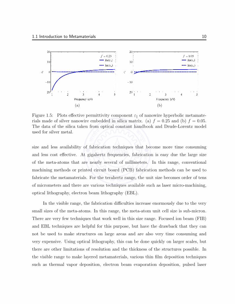
1.5 Plots effective permittivity component ε‖ of nanowire hyperbolic metama-
terials made of silver nanowire embedded in silica matrix. (a) f = 0.25 and
(b) f = 0.05. The data of the silica taken from optical constant handbook
and Drude-Lorentz model used for silver metal. . . . . . . . . . . . . . . . 10
1.6 The schematic for the two step anodization. In this method nanopores
become straight and more organized. . . . . . . . . . . . . . . . . . . . . . 15
1.7 The FESEM images of nanoporous alumina (a) before and (b) after the
pore widening. The pore widening was done in 5% H3PO4 for 90 minutes
at room temperature. . . . . . . . . . . . . . . . . . . . . . . . . . . . . . . 16
1.8 Schematic illustration of two methods for barrier removal. Cross section of
the nanoporous alumina are shown at various stages. (a) The wet etching
process in H3PO4 and (b) shows the voltage/current reduction method. . . 17
1.9 The FESEM images of nanoporous alumina (a) before and (b) after the
barrier layer removal by the cathodic polarization process. (a) Shows
nanopores with the barrier layer at the bottom and bellow the barrier
layer the remained aluminium sheet was used to give the electrical contact
to the cathodic polarization process. (b) Shows the nanoporous alumina
with removed barrier layer by cathodic polarization process. . . . . . . . . 18
1.10 The FESEM images of metalized nanoporous alumina. (a) the bare nanoporous
alumina, (b) the top view of silver nanowire deposited nanoporous alumina
and (c) the cross section of silver nanowire deposited nanoporous alumina.
Reproduced with permission from Sauer et al., Journal of Applied Physics,
91, 3243 (2002). Copyright 2002, AIP Publishing LLC. . . . . . . . . . . . 20
1.11 (a) An arbitrary shape domain for FEM analysis, (b) the domain of (a) is
discretized in few number of sub-domains and (c) domain is discretized in
large umber of sub-domains. . . . . . . . . . . . . . . . . . . . . . . . . . . 22
xvi

1.12 The normalized plots of the field component Ez for TM01 and TM11 modes
at 10 GHz frequency. (a) and (b) are obtained by analytical calculations,
β/k0(TM01)=1.8088 and β/k0(TM11)=1.4668. (c) and (d) are obtained by
COMSOL simulation, β/k0(TM01)=1.8091 and β/k0(TM11)=1.4677. . . . 27
2.1 The photograph of the anodization holder and anodization setup to anodize
the aluminium sheet. (a) the components of the holder, (b) the parts of
holder are assembled and (c) the anodization setup schematic for anodiza-
tion of the aluminium sheet. . . . . . . . . . . . . . . . . . . . . . . . . . . 31
2.2 A schematic for the planar nanoporous alumina. Nanopores are in hexag-
onal arrangement and uniform size throughout. . . . . . . . . . . . . . . . 33
2.3 FESEM images of the planar nanoporous alumina prepared in 0.3 M oxalic
acid solution at 0 C. (a) the top view show the nanopores arrangement
and (b) the cross section in which the nanopores are uniform throughout. . 34
2.4 FESEM images of planar nanoporous alumina obtained by anodization of
aluminium sheet: (a) anodized surface without electropolishing, (b) an-
odized surface after electropolishing and (c) electropolished and scratched
surface that has been subsequently anodized. The corresponding images of
the surfaces of the aluminium sheet, obtained before anodization, are also
shown in (d), (e) and (f) respectively, for comparison. . . . . . . . . . . . . 35
2.5 A schematic of the anodization setup to anodize the aluminium microwire. 38
2.6 Schematic of the structure of the cylindrical nanoporous alumina. (a) an-
odizing aluminium microwire, (b) outer surface of the anodized wire, (c)
the transverse cross section of the anodized wire and (d) the longitudinal
cross section of the anodized wire. . . . . . . . . . . . . . . . . . . . . . . . 39
xvii

2.7 FESEM images of (a) electropolished aluminium wire, (b) anodized wire,
(c) outer surface of the anodized wire, (d) transverse cross section of the
anodized wire. Images (e) and (f) are of hollow nanoporous alumina mi-
crotubes of small and large diameter respectively. . . . . . . . . . . . . . . 40
2.8 (a) An schematic to mill out the part of the cylindrical nanoporous alumina
to see the pore size with respect to radius of the wire and (b) corresponding
the FESEM images of the milled out cylindrical nanoporous alumina. . . . 42
2.9 The measured anodization current of aluminium microwires of diameters
(a) 50 µm, (b) 100 µm and (c) 220 µm. The small jump in the anodization
current of anodization of aluminium microwires of (a), (b) and (c) occurred
around 60 minutes, 70 minutes and 110 minutes respectively. (d) The
anodization current of an aluminium sheet for reference. There is no jump
in the anodization current of aluminium sheet anodization. . . . . . . . . . 45
2.10 FESEM images of anodized wire to show the crack formation in the nanoporous
shell while anodization. (a) No crack for 30 min anodization and (b) sample
just after the crack take place. The anodization time was 70 min. . . . . . 46
2.11 FESEM images of anodized wire to show the curvature effect on the nanopore
size and interpore distance. (a) and (b) for large diameter, and (c) and (d)
for small diameter. . . . . . . . . . . . . . . . . . . . . . . . . . . . . . . . 47
2.12 Optical microscope images in reflection mode of (a) an electropolished alu-
minium wire and (b) anodized wire with hollow core. . . . . . . . . . . . . 48
2.13 FESEM image of Ag nanowires deposited into the pores of the planar
nanoporous alumina. (a) A schematic to electrodeposition of Ag nanowire,
(b) electrodeposited Ag nanowires and (c) the zoomed image of area of
white dotted rectangle in (b). . . . . . . . . . . . . . . . . . . . . . . . . . 50
xviii

2.14 FESEM image of Ag nanowire deposited in the cylindrical nanoporous
alumina. (a) A schematic to electrodeposition of Ag nanowire, (b) elec-
trodeposited Ag nanowires. The white dotted rectangle position of (a) is
shown in (b), (c) the zoomed image of area of white dotted rectangle in (b)
and the EDX spectra of Ag nanowire embedded in nanoporous alumina shell. 52
3.1 The schematic of (a) planar nanoporous alumina where the nanopores are
organized in hexagonal pattern in xy−plane and oriented uniformally along
z−direction, and (b) the top surface area of the planar nanoporous alumina
showing a unit shell. . . . . . . . . . . . . . . . . . . . . . . . . . . . . . . 56
3.2 The schematic of (a) position a cylindrical shell of radius r and (b) a small
local area on the general φz surface at radius r. . . . . . . . . . . . . . . . 59
3.3 Nanopores fill fraction of cylindrical nanoporous alumina when nanopore
diameters are 30 nm and 50 nm at the outer surface. . . . . . . . . . . . . 61
3.4 A cylindrical shell is mapped to a flat slab. The nanopores along the radial
direction in shell mapped along the x-direction in the new frame. . . . . . 62
3.5 The COMSOL calculated, the normalized electric field of (a) anisotropic
cylinder with ¯ε = (1, 1, r20) in an anisotropic medium ¯ε = (εAl2O3 , εAl2O3 , εAl2O3r
20),
(b) anisotropic cylinder with ¯ε = (εAg, εAg, εAgr20) in an anisotropic medium
¯ε = (εAl2O3 , εAl2O3 , εAl2O3r20), (c) isotropic air cylinder with ε = 1 in an
isotropic alumina ε = εAl2O3 and (d) isotropic silver cylinder with ε = εAg
in an isotropic alumina ε = εAl2O3 . The color shows the normalized electric
field and the arrow show the electric field directions. Here εAl2O3 = 2.6375,
εAg = −1359.1400 + i115.5060 and r0 = 12.5µm. . . . . . . . . . . . . . . . 65
xix

3.6 The effective permittivity components of cylindrical nanoporous alumina
with respect to the radius of the wire at 442 nm, 532 nm, 632.8 nm and
785 nm wavelengths. The left panel is for air inclusion and the right panel
is for the silver inclusion. . . . . . . . . . . . . . . . . . . . . . . . . . . . . 67
3.7 The permittivity of (a) pure alumina (Weber, Handbook of Optical Ma-
terials, 2003) and (b) silver metal of Drude model (Cai et al., Optical
Metamaterials: Fundamentals and Applications, 2010). . . . . . . . . . . . 68
3.8 The effective permittivity components of cylindrical nanoporous alumina
at constant nanopore fill fractions of 0.08 and 0.23 with respect to the
frequency. The left panel for air inclusion, and the right panel for silver
inclusion. Here R1=0.5µm and R2=12.5µm. . . . . . . . . . . . . . . . . . 69
4.1 Schematic of the coaxial fiber. The region between R1 and R2 is the
anisotropic cylindrical nanoporous alumina shell. The core (r < R1) and
the outer region (r > R2) of the anisotropic region are the PEC. . . . . . . 76
4.2 Plots of the Bessel functions Jα and Yα (left panel), and plots of the Mod-
ified Bessel functions Iα and Kα (right panel). Plots of (a) and (b) for
integral order, (c) and (d) for fractional order, and (e) and (f) for imagi-
nary order (Olver et al., NIST Handbook of Mathematical Functions,2010). 85
4.3 The behavior of low-order modes (TM1,1 and TM2,2) in an anisotropic
nanoporous alumina coaxial fiber for dimensions R1 = 0.5 µm and R2 =
12.5 µm. Col. 1: Eigen modes at β = 0, τ = m integral order, Col. 2:
modes at εr = 2.467, εφ = εz = 2.638, and β 6= 0, τ 6= m fractional order,
Col. 3: modes at εr = 2.638, εφ = εz = 2.467, and β 6= 0, τ 6= m imaginary
order. Dielectric constants are at wavelength 633 nm. . . . . . . . . . . . . 87
xx

4.4 The computed electric fields (Ez) of modes in cylindrical nanoporous alu-
mina when nanopores have air inclusion for R1 = 0.5 µm, R2 = 12.5 µm for
m = 1, 2, 5, 20, 40. Top row shows the Bessel modes in an isotropic alumina
fiber with real integral orders for εr = εφ = εz = 3.118. The middle row
shows Bessel modes in an anisotropic nanoporous alumina fiber with frac-
tional order and positive dielectric permittivity components for εr = 2.467
and εφ = εz = 2.638. The bottom row shows the fields for Bessel modes of
anisotropic nanoporous alumina fiber with imaginary orders and εr = 2.638
and εφ = εz = 2.467. Relative permittivity components are at wavelength
632.8 nm. . . . . . . . . . . . . . . . . . . . . . . . . . . . . . . . . . . . . 88
4.5 The computed electric fields (Ez) of modes in cylindrical nanoporous alu-
mina when nanopores have silver metal inclusion for R1 = 0.5 µm, R2 =
12.5 µm for m = 1, 2, 5, 20, 40. The fields for Bessel modes of anisotropic
nanoporous alumina fiber with complex orders and εr = −1.288 + i0.053
and εφ = εz = 6.244 + i0.027. Relative permittivity components are at
wavelength 632.8 nm. . . . . . . . . . . . . . . . . . . . . . . . . . . . . . . 89
4.6 The computed TM1,1 dispersive dispersion of modes in cylindrical nanoporous
alumina when nanopores have (a) air inclusion with fill fraction 0.23 and
(b) silver inclusion with fill fraction 0.08. R1 = 0.5 µm, R2 = 12.5 µm.
The air permittivity was 1, the permittivity of alumina taken from Ref.
Rajab et al. 2008 and for silver from Ref. Ordal et al. 1983. . . . . . . . . 92
4.7 The modal dispersions of the homogeneously filled nanoporous alumina
hollow waveguides embedded in air and when the nanopoers are filled with
(a) air for fill fraction 0.23 and (b) silver metal for fill fraction 0.08. The
permittivity of alumina taken from Ref. Rajab et al. 2008 and for silver
from Ref. Ordal et al. 1983. . . . . . . . . . . . . . . . . . . . . . . . . . . 96
xxi

4.8 The normalized mode plots of the homogeneously filled nanoporous alu-
mina waveguide, when the nanopores are filled with air and silver, at wave-
length 632.8 nm. (a) and (b) are modes for air inclusion, εr = 2.638, εφ =
2.467. (c) and (d) are modes for silver inclusion, εr = −1.288+ i0.053, εφ =
6.244 + i0.027. Here the core radius R1 = 5µm and nanoporous alumina
shell radius R2 = 15µm. . . . . . . . . . . . . . . . . . . . . . . . . . . . . 98
5.1 Plot of the fill fraction of nanopores of the cylindrical nanoporous alumina
with microtube radius r and the diameter of the nanopores 2Q at the
outer surface at R2. Here interpore distance D = 100 nm, R1 = 0.5 µm,
R2 = 12.5 µm. . . . . . . . . . . . . . . . . . . . . . . . . . . . . . . . . . 103
5.2 Plots of the effective permittivity components εr and εφ with frequency
and radius of the fiber for 2Q = 50 nm, D = 100 nm. (a) and (b) for 1
THz to 50 THz frequency range, (c) and (d) for the visible range. . . . . . 104
5.3 The modal dispersion plots for inhomogeneous and anisotropic cylindrical
nanoporous alumina coaxial fiber obtained by the COMSOL simulation.
The inner core radius R1 = 0.5µm and the shell radius R2 = 12.5µm.
The nanopores diameter and interpore distance are 50 nm and 100 nm
respectively at the outer surface of the nanopoorus alumina shell. . . . . . 108
5.4 The COMSOL simulated field plots of some hybrid modes of nanoporous
alumina fiber for air inclusion at wavelength λ = 632.8 nm, the inner core
radius R1 = 0.5µm and the shell radius R2 = 12.5µm. The inner and outer
boundaries are PEC. Here there exist only EH hybrid modes. Rows 1 and 2
for inhomogeneous and anisotropic fiber, and rows 3 to 6 for inhomogeneous
and isotropic fiber. . . . . . . . . . . . . . . . . . . . . . . . . . . . . . . . 110
xxii

5.5 The COMSOL simulated field plots of some guided modes of nanoporous
alumina fiber for air inclusion at wavelength λ = 632.8 nm, the inner core
radius R1 = 0.5µm and the shell radius R2 = 12.5µm. Here the core
and the outer regions are filled with air. The nanopores diameter and
interpore distance are 50 nm and 100 nm respectively at the outer surface
of the nanopoorus alumina shell. Modal field plots for inhomogeneous and
anisotropic fiber are in rows 1 and 2, and for inhomogeneous and isotropic
fiber are in rows 3 to 6. . . . . . . . . . . . . . . . . . . . . . . . . . . . . . 112
5.6 The modal dispersion plots for inhomogeneous and anisotropic cylindrical
nanoporous alumina hollow fiber obtained by the COMSOL simulation.
The inner core radius R1 = 0.5µm and the shell radius R2 = 12.5µm.
The nanopores diameter and interpore distance are 50 nm and 100 nm
respectively at the outer surface of the nanopoorus alumina shell. . . . . . 113
5.7 (a) Photograph of light (λ = 532 nm) propagating across a bent nanoporous
alumina fiber with an aluminum core, aluminium core diameter- 10 µm,
nanoporous alumina shell diameter- 80 µm, length- 1.3 cm, nanopore di-
ameter is 30 nm and nanopore periodicity is 100 nm at outer surface. The
scale bar is shown for scale. (b) The output from the nanoporous alumina
fiber at λ = 632.8 nm wavelength. . . . . . . . . . . . . . . . . . . . . . . . 115
6.1 FESEM images of the front surface of planar nanoporous alumina: (a)
before and (b) after the deposition of a 25 nm thick Au film. Image (c)
is the cross sectional image of the Au-coated planar nanoporous alumina
showing the pores and the top gold coating. . . . . . . . . . . . . . . . . . 119
xxiii

6.2 The large-angle scattering and reflectivity spectra obtained by darkfield
and brightfield microscopic measurements. (a) The darkfield (scattering)
spectra when the planar nanoporous alumina (PNA) is coated with 25 nm
thick gold film, (b) the darkfield (scattering) spectra from bare PNA, (c)
the brightfield (reflection) spectra when the PNA is coated with 25 nm
thick gold film and (d) the brightfield spectra (reflection) from the bare
PNA. . . . . . . . . . . . . . . . . . . . . . . . . . . . . . . . . . . . . . . . 121
6.3 Fluorescence spectra obtained from R6G doped PMMA spin coated on the
planar nanoporous alumina (PNA) with and without gold coating using
(a and b) 488 nm and (c and d) 548 nm wavelength excitations. (a) Flu-
orescence spectra when R6G coated on Au-coated PNA, (b) fluorescence
spectra when R6G coated on bare PNA, (c) fluorescence spectra when R6G
coated on Au coated PNA and (d) fluorescence spectra when R6G coated
on bare PNA. . . . . . . . . . . . . . . . . . . . . . . . . . . . . . . . . . . 124
6.4 (a) Schematic of R6G doped nanoporous alumina shell and (b) Fluorescence
photograph of R6G coated nanoporous alumina shell excited by 548 nm
wavelength light. The diameter of the anodized wire was 70 µm. . . . . . . 127
6.5 (a) The darkfield and (b) the brightfield spectra of silver nanowires (NWs)
embedded cylindrical nanopoorus alumina (CNA). All the spectra had been
normalized with an electropolished aluminium micro wire. (c) and (d) are
the optical photograph of the bare CNA and silver nanowire embedded
CNA in the darkfield and the brightfield mode respectively. . . . . . . . . . 129
6.6 Fluorescence spectra of R6G doped in cylindrical nanoporous alumina ex-
cited by (a) 488 nm wavelength and (b) 548 nm wavelength lights. . . . . . 131
xxiv

List of Tables
1.1 The aluminium anodization conditions and the result at parameters of
the nanoporous alumina for some frequently used acids and conditions
(Adapted from Santos et al., Materials, 7, 4297 (2014)). . . . . . . . . . . . 14
4.1 Possible solutions for Hz in a non-magnetic (µr = µφ = µz = 1) homoge-
neous anisotropic circular coaxial waveguide. . . . . . . . . . . . . . . . . . 78
4.2 Possible solutions for Ez in a non-magnetic (µr = µφ = µz = 1) homoge-
neous anisotropic circular coaxial waveguide. . . . . . . . . . . . . . . . . . 81
4.3 The dispersive cutoff frequencies (in THz) of TM modes of a non-magnetic
homogeneous isotropic alumina coaxial fiber. Cutoff frequencies are calcu-
lated in the 1-35 THz frequency range for various modes. . . . . . . . . . . 92
4.4 The dispersive cutoff frequencies (in THz) of TM modes of a non-magnetic
homogeneous nanoporous alumina coaxial fiber for air inclusion in the
nanopores. Cutoff frequencies are in the 1-35 THz frequency range. . . . . 93
4.5 The dispersive cutoff frequencies (in THz) of TM modes of a non-magnetic
homogeneous nanoporous alumina coaxial fiber for silver metal inclusion in
the nanopores. Cutoff frequencies of fibers are in the 1-1500 THz frequency
range. . . . . . . . . . . . . . . . . . . . . . . . . . . . . . . . . . . . . . . 94
xxv

4.6 Guided mode conditions of a non-magnetic homogeneous anisotropic hollow
circular waveguide. Where dielectric constant of core and outer region are
ε1 = ε3 = εi. The index i for isotropic material. . . . . . . . . . . . . . . . 97
5.1 The cutoff frequencies (in THz) of an inhomogeneous and anisotropic nanoporous
alumina coaxial fiber. The cutoff frequencies were calculated for core and
shell radius 0.5 µm and 12.5 µm. The nanopores diameter and interpore
distance are 50 nm and 100 nm respectively at the outer surface of the
nanoporus alumina shell. . . . . . . . . . . . . . . . . . . . . . . . . . . . . 109
xxvi

Chapter 1
Introduction
1.1 Introduction to Metamaterials
The optical properties of various materials and crystals have been studied extensively
and their optical phenomena such as refraction, polarization, birefringence, linear and
non-linear effects etc. are well known [1–5]. The devices have to be designed according
to the properties of the materials because the materials properties can not be changed.
Most of the crystals are optically anisotropic with their optical properties arising from
the atomic/molecular polarizabilities and the arrangement of the atoms in the materi-
als [1, 3, 4]. The anisotropy in natural crystals is, however, very small and the optical
anisotropy can be changed only to a small extent by applying external fields or stresses.
Usually crystals have orthorhombic symmetries and there are no cylindrically or spheri-
cally symmetric anisotropies in the natural crystals. Over the last couple of decades, a new
class of materials are called ‘Metamaterials’, whose electromagnetic or optical properties
can be obtained according to the need [6–8] have been developed. Metamaterials are ar-
tificially designed structured composite materials that utilize resonances of the structure
to control and manipulate the waves and the physical phenomena in them. Properties
of the metamaterials depend on the constituent materials used in their construction as
well as the geometrical structures. Metamaterials are typically obtained by periodically
1

1.1 Introduction to Metamaterials 2
repeating a unit cell called meta-atom that is analogous to an atom or a molecule in
natural materials. These metamaterials can show properties that usually are not found
in natural materials. In general, metamaterials can be designed for any kind of waves
such as electromagnetic waves, acoustic waves, seismic and magnetic spin waves or any
other type of waves, but here in this thesis, our interest is only on metamaterials for
electromagnetic waves with frequencies ranging from microwave (109 Hz) to optical waves
(1015 Hz). Metamaterials are being used for sub-wavelength imaging, superlens, enhanced
spontaneous emission, electromagnetic invisibility and in non-linear applications [7, 8].
In metamaterials, the anisotropy can be changed literally at will. Some of them
even show indefinite behavior for the response tensor [9], which we shall discuss in the
next section. Most of the metamaterials are planar structured metamaterials and provide
novel responses only for waves polarized or incident in specific directions. Thus, unless
designed for isotropic responses, most metamaterials are intrinsically anisotropic. For
example, unidirectionally oriented dilute arrays metal microwires function as a homoge-
neous medium which have very low plasma frequency (109 Hz) and this metal microwire
array medium has uniaxial anisotropy, But if the microwires were uniformly oriented
along all the three directions then the medium would become isotropic [10,11], but would
also have a very small plasma frequency. Some researchers have demonstrated layered
structured metamaterials in half-cylindrical shaped and rolled metamaterials that have
cylindrical symmetry [12–15]. We also note that field cloaking devices mostly are with
cylindrical symmetry [16–18], where these new structured materials play a central role.
But these devices spanning along the longitudinal direction (cylindrical axis) are only a
single meta-atom, and effectively, they appear as two dimensional circular objects due
to the axis of invariance. An optical cloak in the visible frequency made of tiny prolate
spheroids oriented along the radial direction in a cylindrical dielectric medium has also
been theoretically discussed [17]. In a similar manner, an optical cloak, which was made
of uniform metal nanowires embedded in a dielectric medium, was also shown theoreti-
cally only [18]. But no one has yet demonstrated practically radially oriented nanowires

1.1 Introduction to Metamaterials 3
cylindrical system.
In this thesis, we report on the fabrication, characterization and some applications
of radially structured anisotropic metamaterials with cylindrical symmetry. These meta-
materials are truly nano-structured in a three dimensional sense and can be produced
on very large scales in a cost effective manner. These cylindrical metamaterials are not
be limited just to optical applications, but several other applications including thermal
engineering applications, are possible. In the present chapter, we shall introduce the basic
concepts and tools, which will be needed to understand the electromagnetic properties of
cylindrical metamaterials that are the focus of our thesis. In the rest of the chapters, the
fabrication, characterization, modeling and some applications of the radially structured
cylindrical metamaterials are discussed.
1.1.1 Classification of Metamaterials
Since the metamaterials are composite materials, therefore, they are inhomogeneous at
the subwavelength/micron/nano scale but can be described as a homogeneous medium
on length-scales much larger than the wavelength. Homogenization techniques such as
Maxwell-Garnett, Bruggeman formalism, field averaging etc. are deduce to get the ef-
fective parameters that describe the wave propagation in the metamaterials. For valid
homogenization, the size of the unit cell of the metamaterials should be electrically or
magnetically small. We will discuss the Maxwell-Garnett homogenization technique in
the cylindrical geometry in Chapter 3. The effective permittivity and effective permeabil-
ity are two possible parameters by which the metamaterials properties can be described.
By designing the metamaterials with the possible the effective permittivity and effective
permeability, the physical phenomena in the metamaterials can be controlled.
In general, the effective permittivity and effective permeability of an isotropic meta-
material are complex functions of frequency. In metamaterials, the numerical value of
the real part of the effective material parameters may be positive or negative. For the

1.1 Introduction to Metamaterials 4
m
¶ > 0, m > 0¶ < 0, m > 0 kE
Double positive (DPS)Right Handed Medium
Single Negative (SNG)Electric Plasma
Metals below UV
H
Ordinary materialsRight Handed Propagating
waves
Metals below UVEvanescent waves
k
¶ > 0 m < 0¶ < 0 m < 0
k
E
S
Single Negative (SNG)Magnetic Plasmaifi i l i l
Double Negative (DNG)f d d di
¶ > 0, m < 0¶ < 0, m < 0 kH
Artificial metamaterialsSome ferrites
Evanescent waves
Left Handed MediumArtificial metamaterialsLeft handed Propagating
waveswaves
kS
Figure 1.1: A schematic diagram to show the material classification based on the realparts of the material parameters ε and µ plotted along the x and y axes respectively. Herewe only consider isotropic media. The decaying curved line represents the evanescent wavewhile the oscillatory line represents the propagating wave.

1.1 Introduction to Metamaterials 5
sake of simplicity to classify the materials, we here consider then to be isotropic and
lossless when the imaginary part of the medium parameters may be considered to be
negligible. Figure 1.1 show a general classification of materials based on the permittiv-
ity (ε) and permeability (µ) components. The first quadrant corresponds to media with
both parameters being positive called double positive (DPS) media. Most of the natural
materials lie in this region. The electric field ( ~E), magnetic field ( ~H) and propagation
vector (~k) of the electromagnetic wave form a right handed triad. Hence, the materials
that lies in this quadrant are called right handed materials (RHM) also. If either of the
parameters, the permittivity or the permeability become negative, then the metamateri-
als are said to be single negative metamaterials (SNG) and these lie in the second and
fourth quadrants of Fig. 1.1. The most interesting case occurs when both the parameters
simultaneously become negative, then the metamaterials are said to be double negative
metamaterials(DNG) and lie in the fourth quadrant as shown in the Fig. 1.1. If both
the parameters become negative, then negative refraction is possible. In this region, the
vectors E, H and k form a left handed triad, and are called left handed materials (LHM).
Metamaterials can be designed to correspond to any one of these four quadrants.
In general, metamaterials are anisotropic too and their material parameters are
described by second ranked tensors. We know that the anisotropic materials posses a
large variety of interesting properties that are not present in isotropic materials. One
classification that can be made for anisotropic metamaterials depends on the behavior of
the dispersion relations or on the sign of the eigenvalues of the material parameter tensors.
Since the dispersion of a wave in a biaxial anisotropic medium is quite complicated [19],
we shall discuss this aspect in the case of uniaxial dielectric anisotropic metamaterials.
Consider an uniaxial non-magnetic (¯µ = µ0(1, 1, 1)) medium in which the permittivity
tensor is ¯ε = ε0(εx, εx, εz). In this medium the dispersion relation is given by the following
expressionk2x + k2
y
εz+k2z
εx=(ωc
)2
. (1.1)

1.1 Introduction to Metamaterials 6
(a) (b) (c)
Figure 1.2: The iso-frequency surfaces of an uni-axial non-magnetic material. (a) Theiso-frequency surface is an ellipsoid if εx > 0 and εz > 0. (b) The hyperboloid of onesheet for εx < 0 < εz. (c) The hyperboloid of two sheets for εz < 0 < εx.
If in Eq. (1.1), the εx > 0 and εz > 0, then the iso-frequency surfaces (ω=constant)
would be ellipsoids as shown in Fig. 1.2(a). This happens in all natural materials and
most metamaterials as well. If in Eq. (1.1), the metamaterial has εx < 0 and εz > 0, then
the iso-frequency surfaces would be hyperboloids of one sheet (Fig. 1.2(b)). If εx > 0 and
εz < 0 for the metamaterials, then the iso-frequency surfaces would be hyperboloids of
two sheets (Fig. 1.2(c)). The second and third cases have an extreme anisotropy and the
corresponding metamaterials are defined as indefinite metamaterials as the eigenvalues
of the permittivity matrix have no definite sign, or as hyperbolic metamaterials [9] as the
dispersion equation becomes hyperbolic. The hyperbolic metamaterials can be resonance
free and typically exhibit lower losses than the resonant metamaterials.
In general, metamaterials can be fabricated over most of the applicable electromag-
netic spectrum from microwaves to optical frequencies. Metamaterials can be classified on
the basis of the wavelength or frequency regime also. Then the wavelengths are approx-
imately 100 µm to 1 dm, the metamaterials are microwave metamaterials because their
resonance frequencies lie in gigahertz range [10, 11]. In the far infrared regime (approx-
imately 10 µm to 100 µm wavelengths) the resonance frequencies lie in terahertz region
and the metamaterials are called terahertz metamaterials [20–22]. Up to the terahertz

1.1 Introduction to Metamaterials 7
(a) (b)
Figure 1.3: The schematic of two types of the hyperbolic metamaterials. (a) The alter-nating electrically thin layers of metal and dielectric (b) the metal nanowires of electricallysmall diameters embedded in a dielectric host gives the metamaterial of non-resonant type.
frequencies, metals used in the construction of metamaterials can be considered as per-
fect or ohmic conductors. Infrared metamaterials are those with resonance frequencies
at long wave infrared to the short infrared (λ ' 20− 2µm). Metamaterials with smaller
resonance wavelengths are known as near-infrared or optical metamaterials. At these
large frequencies, the electronic inertia (mass) considerably affects the performance and
the skin depth (δ) has to be properly accounted to describe the resonance. In the visible
range, the resonances of metamaterials can occur due to surface plasmon excitations, and
hence, such metamaterials are called plasmonic metamaterials [17,23,24]. In many cases,
the metamaterial unit cell becomes comparable with the wavelength of the interacting
radiation, and in those cases the metamaterials would be more aptly termed as photonic
metamaterials [25–27]. Some very simple and practically possible examples of hyperbolic
metamaterials are the layered metamaterials [12] and nanowire metamaterials [28]. In
Fig. 1.3, these examples of hyperbolic metamaterials are schematically shown.
A metamaterial with alternating layers of a metal and a dielectric effectively behaves
as a hyperbolic metamaterial as shown in Fig. 1.3(a). Consider a layered hyperbolic
medium that is made of alternate layers of electrically thin films of silica (SiO2) and

1.1 Introduction to Metamaterials 8
silver metal with film thicknesses of d1 and d2 respectively. The effective permittivity
can be obtained by noting the requirement of field continuity. If the layers are very thin,
then the fields in them can be assumed to be effectively uniform. If the field is incident
parallel to the interface of the thin films then the electric field components E1 and E2
in the two media on either side of an interface will be continuous. Therefore, averaging
the displacement field across the interface, the parallel component of the relative effective
permittivity can be written as
ε‖ =ε1 + ε2η
1 + η, (1.2)
where η = d2/d1. If the incident field is perpendicular to the thin films interface, then
the displacement field components D1 and D2 will be continuous. Therefore, averag-
ing the electric field components, the perpendicular component of the relative effective
permittivity can be obtained as
ε−1⊥ =
1ε1
+ ηε2
1 + η. (1.3)
The components ε‖ and ε⊥ with the frequency are plotted in Fig. 1.4. The data of
silica has been taken from the optical constant handbook [1] and Drude-Lorentz model
used for silver metal. We see a resonance in the permittivity, as shown in Fig. 1.4.
Further, we note the hyperbolic dispersion that becomes possible for both frequencies
below (ε‖ < 0, ε⊥ > 0) and above (ε‖ > 0, ε⊥ < 0) the resonance frequency.
Plasmonic nanowires embedded in a dielectric medium as shown in Fig. 1.3(b)
show hyperbolic dispersion too. Now consider a medium in which silver metal nanowires
of electrically small diameters are embedded, oriented along one direction in a silica
matrix. Let f be the fill fraction of the nanowires in the silica matrix. Applying the
similar approch of field averaging we shall find the effective permittivity components of
the nanowire hyperbolic media. If the incident field is along the nanowires direction then
the electric field components will be continuous at the interface of the silver nanowire
and the silica matrix, therefore, averaging the electric displacement gives the parallel

1.1 Introduction to Metamaterials 9
(a) (b)
Figure 1.4: Plots effective permittivity components ε‖ and ε⊥ of layered hyperbolicmetamaterials made of alternate layers of silica and silver metal. (a) η = 1.5 and (b)η = 0.5. The data of the silica taken from optical constant handbook and Drude-Lorentzmodel used for silver metal.
components of the permittivity component as
ε‖ = (1− f)ε1 + fε2. (1.4)
On the other hand, ε⊥ can be obtained by some homogenization procedure (see Chapter
3). Figure 1.5 shows the dispersion of a nanowire metamaterials where the silver nanowires
are embedded along one direction in silica matrix.
Up to here, we have discussed briefly about metamaterials and their classifications.
Since the metamaterials are structured composite materials, therefore, the biggest chal-
lenges lie in the fabrication. In the next section, we shall discuss some techniques to
fabricate metamaterials.
1.1.2 Fabrication of Metamaterials
Depending on the electromagnetic spectrum regime at which the metamaterial has to
operate, different fabrication techniques need to be used. As we go from the microwave
to the visible frequency region, the fabrication difficulty increases because of smaller unit
1.1 Introduction to Metamaterials 10
(a) (b)
Figure 1.5: Plots effective permittivity component ε‖ of nanowire hyperbolic metamate-rials made of silver nanowire embedded in silica matrix. (a) f = 0.25 and (b) f = 0.05.The data of the silica taken from optical constant handbook and Drude-Lorentz modelused for silver metal.
size and less availability of fabrication techniques that become more time consuming
and less cost effective. At gigahertz frequencies, fabrication is easy due the large size
of the meta-atoms that are nearly several of millimeters. In this range, conventional
machining methods or printed circuit board (PCB) fabrication methods can be used to
fabricate the metamaterials. For the terahertz range, the unit size becomes order of tens
of micrometers and there are various techniques available such as laser micro-machining,
optical lithography, electron beam lithography (EBL).
In the visible range, the fabrication difficulties increase enormously due to the very
small sizes of the meta-atoms. In this range, the meta-atom unit cell size is sub-micron.
There are very few techniques that work well in this size range. Focused ion beam (FIB)
and EBL techniques are helpful for this purpose, but have the drawback that they can
not be used to make structures on large areas and are also very time consuming and
very expensive. Using optical lithography, this can be done quickly on larger scales, but
there are other limitations of resolution and the thickness of the structures possible. In
the visible range to make layered metamaterials, various thin film deposition techniques
such as thermal vapor deposition, electron beam evaporation deposition, pulsed laser

1.2 Role of Metamaterials in Waveguides and Optical Fibers 11
deposition, sputtering etc. are suitable. The template method, which will be discussed
in later sections of this chapter, is one of the best method to fabricate nanostructured
or nanowire metamaterials. Using this method highly organized nanomaterials and very
high aspect ratio nanowire metamaterials can be fabricated on large scales. Nanoporous
alumina templates are widely used to fabricate such nanowire metamaterials. In fact, this
template technique is not only suitable for visible range metamaterial fabrication but may
be suitable for near infrared metamaterials too by tuning the template structure using
the fabrication parameters.
This thesis discusses the fabrication of the cylindrical metamaterials using nanoporous
alumina templates, and their application as metamaterial waveguides and optical fibers
by themselves. Hence, in the next section, we shall briefly introduce the development of
metamaterial inclusions in waveguides and optical fibers.
1.2 Role of Metamaterials in Waveguides and Optical
Fibers
Optical fibers form the backbone of optical communications systems worldwide. Their
analogues in the microwave regime are hollow or coaxial metallic waveguides, which are
indispensable in applications requiring field confinement, low losses, and high power-
handling capability. The introduction of physical structure in the form of a periodic array
of microscopic air holes running along the fiber axis in the photonic crystal fiber [29] gives
rise to new possibilities. Light can even be confined within a hollow core or a core of lower
refractive index due to confinement caused by a photonic band gap in the surrounding
region containing a periodic array of holes. Alternatively for a solid core surrounded by
microholes, the clad region with the microholes effectively creates a region with lower
modal index for light propagating in the core and confines light by a modified total-
internal-reflection effect. Birefringence of the modes in these fibers usually results from
a two-fold asymmetry, and even small birefringence created by applied strain provides

1.2 Role of Metamaterials in Waveguides and Optical Fibers 12
for many sensor applications [30]. However, these fibers usually have no structure or
structural anisotropy perpendicular to the fiber axis.
Introducing the metamaterial in the design of the optical fiber or waveguide can give
rise to some unique properties which can not be found in conventional optical fibers or
waveguides. Interesting phenomena have been shown in microwave rectangular and circu-
lar waveguides loaded with metamaterials, including propagation at frequencies below the
fundamental mode of the unfilled waveguide [31,32]. Similarly, the unprecedented control
over the metamaterial properties as well as the enormous flexibility of applications possi-
ble with a fiber makes it attractive to combine them into a common platform. Theoretical
discussions of fibers made of negative-refractive-index materials have indicated interesting
properties such as sign-varying energy flux [33] and zero group-velocity dispersion [34].
Surface waves guided along a cylindrical metamaterial waveguide were discussed in [35].
Dispersion of modes in a fiber with anisotropic dielectric permittivity was also discussed
recently [36]. However, the immense difficulty of practically assembling small nanostruc-
tured metamaterial units inside the micrometer sized fibers has essentially discouraged the
discussion of such systems for optical frequencies. Only some cylindrically layered tubes,
or those with coaxially oriented nanowires that are otherwise uniform along the axis, have
been theoretically discussed [37, 38] as metamaterial optical fibers. These layered tubes
due to the inherent anisotropy of the layered structure as explained in the section 1.1,
provide an anisotropic waveguide with cylindrical symmetry. Recently, guided modes in a
hollow core waveguide with a uniaxial metamaterial cladding have been theoretically dis-
cussed [39], where the metamaterial was proposed to consist of a layer of drawn split-ring
resonators. The dispersion of the transverse components of the magnetic and dielectric
properties of the metamaterial clad was found to dominate the behavior of the modes [40]
and a drawn fiber with a single split-ring resonator at the fiber axis was demonstrated
for terahertz frequencies in [41]. We note that all the proposals for metamaterial fibers so
far have considered only designs that are invariant and homogeneous along the fiber axis,
i.e., effectively the problem is only two-dimensional, presumably because only the drawing

1.3 Nanoporous Alumina 13
technique was considered for the fabrication of these fibers. This limits the discussion to
a form of anisotropy with effective dielectric parameters εr ' εφ 6= εz.
In the later chapters of this thesis, we shall show that application of anodization
techniques [42] to aluminum microwires can result in a three-dimensionally radially struc-
tured cylindrical metamaterial and can be used as an anisotropic metamaterial optical
fiber made of nanoporous alumina (Al2O3). In the next section, we shall introduce about
the anodization technique to form nanoporous alumina and its use as a template in fab-
rication of nanowire metamaterials.
1.3 Nanoporous Alumina
Nanoporous alumina are aluminium oxides having nanopores that self organize and get
arranged in a hexagonal ordered lattice during anodization. These are obtained by an-
odization of aluminium sheets in an acidic environment [42]. While anodization, at the
anode the liberation of hydrogen gas bubbles create nanopores and to minimize the energy
of the system the nanopores arranged themselves in an hexagonal order. For the anodiza-
tion of an aluminium sheet, various acids such as sulfuric acid, oxalic acid, phosphoric
acid and many more can be used [43] to obtain nanopores with different size and spac-
ing. The anodization starts from the surface of the aluminium sheet and the nanopores
grow perpendicular to the surface [44]. Ideally, the nanopores are organized in a hexag-
onal pattern. The nanopore sizes, organization and interpore distances depend on the
aluminuim purity, surface roughness, electrolyte nature, anodization voltage or current,
temperature, number of anodization steps and time [43]. The organization of nanopores
even for very pure aluminium sheet can be changed by pre-texturing the aluminium sheet
surface [45,46]. Some typical acids and parameters of their anodized products under some
typical conditions are listed in Table 1.1. Increasing the acid temperature and keeping all
other parameters constant will increase the nanopore size, interpore distance as well as
the ordering of the nanopores. But with increasing temperature, decreases the ordering

1.3 Nanoporous Alumina 14
Table 1.1: The aluminium anodization conditions and the result at parameters of thenanoporous alumina for some frequently used acids and conditions (Adapted from Santoset al., Materials, 7, 4297 (2014)).
Acid Concentration V T dp dint Growth rate(M) (V) (C) (nm) (nm) (µm.h−1)
H2SO4 0.3 25 5-8 25 63 7.5H2SO4 0.3 40 0-1 30 78 85
H2C2O4 0.3 40 5-8 50 280 3.5H2C2O4 0.3 140 0-1 30 100 50H3PO4 0.1 195 0-1 160 500 2
of the nanopores. So to get higher ordered nanopores, the anodization should be carried
out at lower temperatures. The optical transparency also depends on the fabrication pa-
rameters which we shall show in the Chapter 2. Nanopore size and interpore distance
increase with acid concentration also.
1.3.1 The Two-Step Anodization
In the previous subsection, we mentioned that the nanopore ordering depends on the num-
ber of steps of anodization and its time. If the aluminium sheet is anodized once then the
nanopores do not form as straight pores and not arranged in hexagonal order [42,47]. This
anodization is called first anodization. Merging of nanopores or branching of a nanopore
may happen in the nanoporous alumina obtained after the first anodization. This is due
to the influence of surface inhomogeneities, stresses etc. If the alumina is subsequently
etched off, the we get a nanosize concave pre-textured aluminium surface [47]. The re-
anodization of alumina etched aluminium sheet at same parameters gives rise to highly
ordered and straight nanopores as the original surface inhomogeneties have no effect now.
This subsequent re-anodization is called the second anodization, and the whole process is
called a two-step anodization process [42]. The Fig. 1.6 shows schematically the two-step
anodization technique. At fixed parameters of the anodization, the size of nanopores and

1.3 Nanoporous Alumina 15
First anodizationSmooth electropolished
Disturbed nanoporousl ielectropolished
anodized Al sheetalumina
Remaining Al sheet
Acid etching of Al O
Pretextured aluminium substrate
Acid etching of Al2O3
Second anodization
Highly ordered nanoporous alumina
Figure 1.6: The schematic for the two step anodization. In this method nanoporesbecome straight and more organized.
the lattice size are also fixed. But after the anodization, the size of the nanopores can be
increased by widening the nanopores by slow dissolution in dilute phosporic acid. Pore
widening can be carried out only up to the interpore distance otherwise the nanopores
would merge into each other and the whole nanoporous alumina network would get dis-
solved by the phosphoric acid. In Fig. 1.7 the FESEM images of nanoporous alumina
before and after pore widening in a 5% phosphoric acid are shown. The anodization time
was 90 minutes at room temperature. It can be seen in Fig. 1.7(b) that if the pore
widening would be carried out for more time, then the nanopores would merge with each
other.
1.3.2 Barrier layer removal
After the anodization process, at the bottom of the nanoporous alumina, an impermeable
insulating alumina barrier layer is left behind followed by conducting aluminium. To
electrodeposit some metal into the nanopores, we have to remove the impermeable barrier
layer and it can be removed by several methods. The common method is the wet chemical
etching. It is carried out by putting the nanoporous alumina into dilute phosphoric

1.3 Nanoporous Alumina 16
(a) (b)
Figure 1.7: The FESEM images of nanoporous alumina (a) before and (b) after the porewidening. The pore widening was done in 5% H3PO4 for 90 minutes at room temperature.
acid after removing the bottom aluminium in some salt electrolytes such as chromic
acid [48]. This procedure is illustrated schematically in Fig. 1.8(a). This method is
good to remove the barrier layer from a thicker nanoporous alumina templates. In thin
nanoporous alumina, after dissolving the supporting aluminium sheet at the bottom, it
is very difficult to handle the micrometer thick templates.
A second method of barrier layer removal is the voltage or current reduction method.
The fact that the barrier layer thickness increases with the anodization voltage or cur-
rent in utilized here. In this method at the end of the anodization process, the voltage
or current are reduced slowly so that the impermeable layer thickness gets drastically
reduced and becomes porous as well. This need to be carried out in a very controlled
manner otherwise small fluctuations of the voltage or current might increase the barrier
thickness [47]. Using this method, there will still be left a 1 to 2 nm thick barrier layer.
After this stage the nanoporous alumina with aluminium at bottom can be used for AC
electrodeposition [47]. The remaining barrier layer can be further removed by dissolving it
in phosphoric acid wash. This method is good for thin or thick both types of nanoporous
alumina because at the bottom there will be the aluminium sheet left for mechanical
support. The second method of barrier layer removal by voltage or current reduction is
shown schematically in Fig. 1.8(b).

1.3 Nanoporous Alumina 17
Second anodizationSecond anodization
Al substrate removed
Barrier removed in H3PO4
Seed layer and metal filling
(a)
Second anodizationSecond anodization
Pore widening
Thinning of the barrier
Metal filling
(b)
Figure 1.8: Schematic illustration of two methods for barrier removal. Cross sectionof the nanoporous alumina are shown at various stages. (a) The wet etching process inH3PO4 and (b) shows the voltage/current reduction method.

1.3 Nanoporous Alumina 18
500 nmBarrier layer at bottom of nanopore
(a) (b)
Figure 1.9: The FESEM images of nanoporous alumina (a) before and (b) after thebarrier layer removal by the cathodic polarization process. (a) Shows nanopores with thebarrier layer at the bottom and bellow the barrier layer the remained aluminium sheetwas used to give the electrical contact to the cathodic polarization process. (b) Showsthe nanoporous alumina with removed barrier layer by cathodic polarization process.
A third method of barrier layer removal is called cathodic polarization. In this
method, after the anodization process is complete, a reverse electrolysis of the alumina
template is further done. The alumina template is used as cathode and graphite or
platinum as anode in a diluted potassium chloride solution [48], and by applying a negative
potential to the alumina template, the barrier layer gets removed electrolytically. A
FESEM of the cross section of the nanoporous alumina with the barrier layer and with
the barrier layer removed is shown in Fig. 1.9. This method needs good optimization. If
the polarization time is less, then the barrier layer would not be fully removed and if the
time become more then it would corrode the aluminium also. This method works well
for thinner nanoporous alumina. The cathodic polarization also widens the size of the
nanopores. For thicker nanoporous alumina, the polarization time would be more and
this causes the nanopores merge with each other. So it can not be used easily for thicker
nanoporous alumina.
We have discussed some methods to remove the barrier layer from nanoporous alu-
mina. After removing the barrier layer, the nanoporous alumina can be used as templates

1.4 Electrodeposition and the Nanowire Metamaterials 19
to grow metal nanowires for plasmonic and metamaterial study. In next section we shall
discuss about the metal nanowire deposition into the nanopores of the nanoporous alu-
mina and the application as nanowire metamaterials.
1.4 Electrodeposition and the Nanowire Metamate-
rials
In fact, nanoporous alumina themselves are structured anisotropic materials that can work
as metamaterials. The nanoporous alumina can be further used as templates to fabricate
one dimensionally oriented thin wire composite structures. After removing the barrier
layer, the nanopores can be filled by some materials such as metals, polymer, dimers,
nanotubes, nanoparticles etc. [46]. External materials filled nanoporous alumina also
works as metamaterials [28]. By filling the nanopores with certain materials, the alumina
matrix can be dissolved in some electrolyte and the nano objects (typically nanowires)
can be separated [49,50]. Thus it becomes a means for the uniform synthesis of nanowires.
We are interested here in the deposition of metal nanowire inside the nanoporous alumina.
The metal nanowires synthesis using the nanoporous alumina template is mainly
done by AC or DC electrodeposition techniques. If we remove the barrier layer by a wet
etching method, then we are left with only nanoporous alumina. A thin or thick layer of
a conductor like silver or gold need to be deposited at one face of the nanoporous alumina
as a seed layer. This nanoporous alumina is used as the cathode and graphite or platinum
as the anode in a metal salt solution of interest. By applying an AC or DC voltage to
the electrodes, the metal nanowires can be deposited into the pores of the nanoporous
alumina [51]. If the barrier layer is removed by voltage reduction or cathodic polarization
method, then the template can be used directly for electrodeposition without any seed
layer [47]. In Fig. 1.10, the FESEM image of silver nanowire grown in the alumina
template is shown. Figure 1.10(a) shows alumina template with the barrier layer removed.
Figure 1.10(b) and Fig. 1.10(c) show the top view and cross section of silver nanowires

1.4 Electrodeposition and the Nanowire Metamaterials 20
(a) (b) (c)
Figure 1.10: The FESEM images of metalized nanoporous alumina. (a) the barenanoporous alumina, (b) the top view of silver nanowire deposited nanoporous aluminaand (c) the cross section of silver nanowire deposited nanoporous alumina. Reproducedwith permission from Sauer et al., Journal of Applied Physics, 91, 3243 (2002). Copyright2002, AIP Publishing LLC.
electrodeposited inside the pores of the nanoporous alumina template respectively. Since
at the bottom there is an aluminium base, therefore, after dissolving the alumina matrix
one can obtain free standing nanowires. Very high aspect ratio nanowires can not be
obtained as free standing nanowires because the nanowires will tend to collapse [52].
There are several applications of nanowire embedded nanoporous alumina. But
here our primary interest is in its use as nanowire metamaterials. Nanowire embedded
nanoporous alumina exhibit the hyperbolic dispersion, and these metamaterials can also
show the negative refraction phenomena [51]. Here the negative refraction happen because
of the hyperbolic nature instead of a negative refractive index. It can be used as a
hyperbolic flat lens [53]. The nanowire metamaterials can be made over very large areas.
The nanowire metamaterials are only two dimensional because the nanopores and the
nanowire growth occur only along one direction. In literature, the nanowire metamaterials
are only known in flat geometry. This thesis will deal with nanowire metamaterials in the
cylindrical geometry, which is discussed in the later chapters.
1.5 The Finite Element Method 21
1.5 The Finite Element Method
As we know, most of the electromagnetic metamaterial structures are very complex sys-
tems to model. In general, only few problems with some symmetries can be approximately
solved analytically, but most of the structures are not amenable to analytical solutions.
To solve such complex systems, there is a need for numerical techniques that can be imple-
mented on computers. There are various numerical techniques such as the finite difference
time domain (FDTD), the finite element method (FEM), method of moments, mesh free
method etc. In this thesis, we have used a commercial simulation software, COMSOL
multiphysics 4.4, which is based on the FEM to model our metamaterial structures. In
this section, we introduce some basic concepts about the FEM and method used in the
COMSOL multiphysics software.
Many physical systems can be represented by partial differential equations. By solv-
ing the set of differential equations with proper boundary conditions, the properties of
the system can be obtained. The FEM is a numerical technique to find the approxi-
mate solutions of physical problems represented by the partial differential equations with
well defined the boundary conditions. For the FEM analysis in a domain there are four
major steps: 1. Discretization into sub-domains or elements, 2. Deriving the differen-
tial equations in the element, 3. Assembling all the elements into the solution domain
and 4. Solving the system of differential equations by applying the boundary conditions.
Now we briefly describe the each steps of the FEM process by a qualitative analysis of
electromagnetic problems [54,55].
1. Consider an arbitrary object where we want to find some electromagnetic quanti-
ties. We first derive the domain of interest into sun-domains or elements as shown in Fig.
1.11. We see that if the number of sub-domains are not sufficient then the discretized
domain would be very roughly matched and the solution too would be very approxi-
mate. On the other hand, if the number of sub-domains are sufficiently large, then the
descretized domain would be better match the original domain and the solution would be

1.5 The Finite Element Method 22
(a) (b) (c)
Figure 1.11: (a) An arbitrary shape domain for FEM analysis, (b) the domain of (a) isdiscretized in few number of sub-domains and (c) domain is discretized in large umber ofsub-domains.
more accurate. Let Vi be the potential in the ith element of the discetrized domains. The
total potential of whole domain would be
V (x, y) =N∑i=1
Vi(x, y) (1.5)
where N is the total number of the sub-domains. Most common forms of the potential
for triangular mesh is
Vi(x, y) = a2x+ a1y + a0 (1.6)
and for quadrilateral mesh is
Vi(x, y) = a3x+ a2xy + a1y + a0. (1.7)
The triangular or quadrilateral mesh are chosen to minimize the irregularity of the de-
scretized domain with the original one. In general, it is approximated that the potential
Vi is zero outside of the ith element. For the triangular mesh we assumed in Eq. (1.6)
potential is linear but in general it may have some other variations also. The electric field
associated with Vi would be
~Ei = −~∇Vi. (1.8)
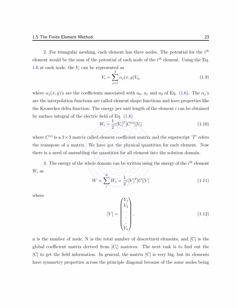
1.5 The Finite Element Method 23
2. For triangular meshing, each element has three nodes. The potential for the ith
element would be the sum of the potential of each node of the ith element. Using the Eq.
1.6 at each node, the Vi can be represented as
Vi =3∑j=1
αj(x, y)Vij (1.9)
where αj(x, y)’s are the coefficients associated with a0, a1 and a2 of Eq. (1.6). The αj’s
are the interpolation functions are called element shape functions and have properties like
the Kronecker delta function. The energy per unit length of the element i can be obtained
by surface integral of the electric field of Eq. (1.8)
Wi =1
2ε[Vi]
T [C(i)][Vi] (1.10)
where C(i) is a 3×3 matrix called element coefficient matrix and the superscript ’T ’ refers
the transpose of a matrix. We have got the physical quantities for each element. Now
there is a need of assembling the quantities for all element into the solution domain.
3. The energy of the whole domain can be written using the energy of the ith element
Wi as
W =N∑i
We =1
2ε[V ]T [C][V ] (1.11)
where
[V ] =
V1
V2
.
.
.Vn
, (1.12)
n is the number of node, N is the total number of descretized elements, and [C] is the
global coefficient matrix derived from [Ci] matrices. The next task is to find out the
[C] to get the field information. In general, the matrix [C] is very big, but its elements
have symmetry properties across the principle diagonal because of the some nodes being

1.6 Modelling in COMSOL Multiphysics 24
connected to each other. We see Fig. 1.11 that as the number N increases the nodes will
increase and it will take more time and computation to solve. Now we shall apply some
other constraints to get the coefficient matrix.
4. From the calculus of variations, we know that the Laplace’s equation is satisfied
when the energy of the whole system is a minimum. So the partial derivative of energy
W with respect to the potential at each node will be zero∂W
∂Vk= 0, k = 1, 2, ..., n. (1.13)
Using the Eq. (1.11) in Eq. (1.13), we get the following expressionn∑i=1
ViCik = 0, (1.14)
where n is the number of nodes in the mesh of the discretized domain. This is a general
expression. If we write the this expression for all nodes, then we get the set of n partial
differential equations in N unknowns, which we have to solve simultaneously to get [V].
There are several methods such as the iteration method [56], matrix method [57] etc.
which can be used to solve the system of partial differential equations.
We have given a general qualitative description of the FEM analysis. Solving manu-
ally such large system of equations of system is not possible, particularly, if the discretized
elements are very large or the system is highly complex. Now-a-days, there are several
software packages that have been developed to solve such type of problems working on the
principles of FEM. We have used the COMSOL Multiphysics, a commercial simulation
software based on FEM to model our metamaterial structures. In the next section, we
introduced briefly about this software.
1.6 Modelling in COMSOL Multiphysics
In COMSOL, there are different types of physical problems such as mechanical, chemical,
electromagnetics, thermal etc., individually or in coupled form, that can be modeled using

1.6 Modelling in COMSOL Multiphysics 25
the different modules. Some major steps of modelling in COMSOL Multiphysics are listed
below:
1. Choosing the appropriate module
2. Drawing the geometry of the system domain
3. Filling the domain with material parameters
4. Applying the appropriate boundary conditions
5. Setting the study parameters such as frequency, wavelength etc, and computation
6. Meshing or discritization of the domain
7. Results analysis such as field plotting, mode analysis, eigenvalues etc.,
For the study of electrodynamics problems, we can choose the Radio Frequency
(RF) module and for optics problems Wave Optics module or RF module. After choosing
the regime of the physics we have to draw the geometry either 2D or 3D. Externally made
CAD geometry from other softwares also can be imported into COMSOL Multiphysics.
The MATLAB software is fully integrated with COMSOL Multiphysics. The problems
script written in MATLAB can be loaded in COMSOL Multiphysics for simulation. If
3D problems takes much time to be solved than the 2D problems, depending on the
available symmetries, the 3D problems can be projected into 2D geometries to reduce the
computation time and memory required.
After drawing the geometry of the problem, we need to feed the material properties
in the volumes of the geometry or sub-geometries. Different kinds of predefined material
parameters are given in COMSOL Multiphysics, but the external material data called user
defined data can be also loaded. The user defined material data can even be parametrized,
spatially or temporally. When the material parameters have been fixed, then there is need
of applying the appropriate boundary conditions. We have carried out electromagnetic
simulations for our analysis. So from now onward for discussion of simulation in COMSOL
Multiphysics, we will focus only on RF module. In the RF module, there are several types
of boundary conditions that are available in COMSOL Multiphysics. One should be very
careful in applying the boundary conditions, otherwise slightly changing them will result in

1.6 Modelling in COMSOL Multiphysics 26
inappropriate solutions. For example, if there is any metallic or magnetic materials in the
domain then we can use perfect electric conductor (PEC) or perfect magnetic conductor
(PMC) boundary conditions. For radiating problems, the scattering boundary conditions
or perfectly matched layer (PML) boundary conditions are good [58–61]. Most of the
metamaterial structures are periodic, in which case, the periodic boundary conditions or
Floquet boundary conditions [60,61] are appropriate.
After fixing the boundary conditions, the next important step is the meshing or dis-
critization. Depending on the size of sub-geometries, the incident frequency, metamaterial
element and space symmetry, there is need to properly mesh the computational domain.
Simulation of 3D problems are more difficult than the 2D problems because for the same
size of meshing in 3D model the number of elements increases exponentially compared
to 2D model and hence the computational time and memory increase drastically. So if
possible, it is always preferable to use a 2D model instead of a 3D geometry. Once the
meshing is done, the simulator is ready to solve or compute the problem. There are differ-
ent types of solver such as stationary solver, time-dependent solver, eigenvalue solver etc.
in COMSOL Multiphysics. The solvers compute almost all the related physical parame-
ters. After the simulations, there is a need to analyze the results by plotting, calculating
various quantities etc.
To benchmark the COMSOL computation, we considered an example of dielectric
circular waveguide from a book ‘Advanced Engineering Electromagnetics’ [62]. A lossless
dielectric circular waveguide of radius 1.3457 cm and dielectric constant 4 is surrounded by
a perfect perfect electric conductor. Analytically, its cutoff frequencies for the TE11 and
TM01 modes are 3.2664 GHz and 4.2664 GHz respectively. We simulated this example in
COMSOL Multiphysics using the RF module’s eigenfrequency module. For the waveguide
modal analysis, the COMSOL solves the following equation
~∇× µ−1r
(~∇× ~E
)− k2
0
(εr −
iσ
ωε0
)~E = 0, (1.15)
where all symbols are in standard notations. The Eq. (1.15) is a general form of the

1.7 Thesis Organization 27
(a) (b) (c) (d)
Figure 1.12: The normalized plots of the field component Ez for TM01 and TM11
modes at 10 GHz frequency. (a) and (b) are obtained by analytical calculations,β/k0(TM01)=1.8088 and β/k0(TM11)=1.4668. (c) and (d) are obtained by COMSOLsimulation, β/k0(TM01)=1.8091 and β/k0(TM11)=1.4677.
Maxwell curl equation. COMSOL calculates all the related parameters with boundary
conditions. The computed cutoff frequencies for TE11 and TM01modes are 3.2641 GHz
and 4.2633 GHz respectively. At 10 GHz frequency, analytically calculating the effective
propagation constant (β/k0) for TM01 and TM11 modes, we obtain the eigenvalues as
1.8088 and 1.4668 respectively, and COMSOL obtained β/k0 for TM01 and TM11 modes
as 1.8091 and 1.4677 respectively. The normalized field component Ez for TM01 and
TM11 modes are plotted in Fig. 1.12. The analytical and computed cutoff frequencies
and effective propagation constants almost match exactly with a very small error since the
FEM analysis gives only the approximate solutions. Error may depend on the limitations
of boundary conditions, size of meshing and the solver.
1.7 Thesis Organization
The present Chapter 1 introduced the basics concepts of metamaterials, classifications,
nanoporous alumina fabrication techniques, nanowire metamaterials, metamaterial waveg-
uides and FEM modeling techniques. The organization of the rest of the chapters of the
thesis is given below.
Chapter 2 discusses the details of the experimental aspects of the fabrication of the

1.7 Thesis Organization 28
metamaterials using nanoporous alumina templates. In this chapter, description of the
fabrication of planar and cylindrical nanoporous alumina templates, and their structural
and morphological characterization will be given. The deposition of metallic nanowires
in these templates also will be described.
Chapter 3 will show the homogenization of cylindrical metamaterials made by cylin-
drical nanoporous alumina templates. We use the technique of transformation optics
and local Maxwell-Garnett homogenization (MGH) theory to homogenize the cylindrical
metamaterials.
Chapter 4, we approximate that our cylindrical nanoporous alumina are homoge-
neously filled. Using this approximation we discuss the properties of anisotropic waveg-
uides that are homogeneously filled, and cylindrical anisotropic nanoporous alumina coax-
ial and hollow fibers.
In Chapter 5, we relax the assumption of the homogeneously filled condition used in
the Chapter 4. We discuss the waveguide properties of the radially inhomogeneous and
anisotropic nanoporous alumina coaxial and hollow fibers. In this chapter, we discuss the
light transmission also in the inhomogeneous and anisotropic nanoporous alumina fibers.
Chapter 6 will discuss the scattering applications of the planar and the cylindrical
nanoporous alumina templates. In this chapter, first we discuss the polarization dependent
light scattering properties and fluorescence properties of the planar nanoporous alumina
which have linearly organized or disorganized nanopores. Later in this chapter, we give
the analysis of the light scattering and fluorescence properties of cylindrical nanoporous
alumina.
Chapter 7 summarizes the thesis and discusses future possible areas of research with
planar and the cylindrical nanoporous alumina.

Chapter 2
Fabrication of Nanoporous AluminaTemplates
2.1 Introduction
In the introductory Chapter 1, we have discussed the basics of nanoporous alumina. The
anodization technique is known since decades [42, 63, 64] for fabricating large areas of
nanoporous alumina with high aspect ratio pores from aluminium sheets. The possibility
of structural modification of nanopores in the nanoporous alumina makes it a very flexible
system for creating templates to deposit other materials. This technique has been also
used to make highly anisotropic nanowire metamaterials [28] but is in the planar geometry.
Nanoporous alumina in the cylindrical geometry has been rarely reported [65–67] and
have been used for chemical catalysis [65, 66]. Alumina membrane microtubes for use
as low friction hypodermic needles has also been reported [67]. In the previous reports,
only alumina membrane tubes with large diameters have been used. The anodization of
cylindrical aluminium wires with diameters of sub-hundred micrometer, and their detailed
structural characterization and optical properties were not known. Nanoporous alumina
in the cylindrical geometry have very different properties from the usual nanoporous
alumina in their structural and anodization characteristics. Our main interest in the
29

2.2 Anodization of Aluminium Planar Sheet 30
thesis are microwires of nanoporous alumina. In this chapter we shall discuss the details
of the fabrication of the nanoporous alumina in planar and cylindrical geometries, their
structural characterization and deposition of nanowires into the porous templates. The
structural characterization has been carried out by using field emission scanning electron
microscope (FESEM), focused ion beam (FIB) and optical microscopy. In this chapter,
it is shown how the cylindrical nanoporous alumina is structurally different from planar
nanoporous alumina. Later on, silver metal deposition has been carried out with both
types of nanoporous alumina. The electrodeposition of silver nanowires in the nanopores
of planar nanoporous alumina is easy because the barrier layer can be easily removed and
the nanopores are uniform throughout the volume. It is, however, very difficult in case of
cylindrical nanoporous alumina as the barrier layer directly can not be removed and the
nanopores diameter decreases radially towards the center.
2.2 Anodization of Aluminium Planar Sheet
A home made anodization holder, made of delrin polymer, has been used to anodize the
aluminium sheet. The anodization holder and setup are shown in Fig. 2.1. A photograph
of the anodization holder (component wise) is shown in Fig. 2.1(a) and the assembled
form of the holder is shown in Fig. 2.1(b). The anodization setup is schematically shown
in Fig. 2.1(c). An Aplab regulated DC power supply (model:L1281) has been used in the
electropolishing, anodization and electrodeposition processes.
2.2.1 Nanoporous Alumina with Highly Organized nanopores
Anodization
Templates were fabricated by a two-step anodization process. Aluminium sheets of
99.999% purity (Alfa Aesar) were cleaned in acetone and then annealed at temperature
500 C in vacuum to increase the gain size. The annealed sheets were electropolished in a

2.2 Anodization of Aluminium Planar Sheet 31
(a) (b)
(c)
Figure 2.1: The photograph of the anodization holder and anodization setup to anodizethe aluminium sheet. (a) the components of the holder, (b) the parts of holder areassembled and (c) the anodization setup schematic for anodization of the aluminiumsheet.

2.2 Anodization of Aluminium Planar Sheet 32
mixture of ethanol and perchloric acid in 5:1 volume ratio at 0.076 A/cm2 current density
for three minutes [68–70]. After electropolishing a very smooth mirror like shiny surface
was obtained which is very necessary to get straight nanopores. The electropolished alu-
minium sheets were anodized in 0.3 M oxalic acid at 40 V at 0 C for half hour [42, 46].
Since the anodization is an exothermic process, we used the ice bath to keep temperature
of the system constant at 0 C. A tantalum (Ta) plate used as the counter electrode. Dur-
ing anodization, the solution was continuously stirred using a magnetic stirrer to keep the
solution temperature uniform. The alumina synthesized in the first anodization process
was etched off in a mixture of chromic acid (9 gm), phosphoric acid (7 ml) and deionized
(DI) water in a 200 ml solution at 90 C [46,48,68]. The alumina etched sample was once
again anodized in 0.3 M oxalic acid. In the second anodization process, all the parameters
were maintained the same as for the first anodization. The second anodization time was
varied as per need. From the anodized sheets, the remaining aluminum was removed by
dissolving in a mixture of hydrocloric acid (100 ml), cupric chloride (3.4 gm) and water
in 200 ml solution. The duration of the alumina etching after the first anodization and
the aluminium etching after second anodization depend on the thickness of the alumina
and aluminium, which we have to optimize for the particular thickness. Pore widening
and barrier layer removal was carried out in 5% phosphoric acid.
Structural Characterization
In Fig. 2.2, a schematic picture of the anodization of plane aluminium sheet is shown.
In nanoporous alumina, the nanopores ideally have a hexagonal arrangement, and the di-
ameters of the nanopores are uniform throughout. The nanopore organization, nanopore
diameter and interpore distance depend on the purity of the aluminium sheet, the sur-
face roughness of aluminium sheet, the nature of electrolyte, applied voltage or current,
temperature of the solution, the first anodization duration. FESEM images of planar
nanoporous alumina are shown in Fig. 2.3. It can be seen in Fig. 2.3(a) that the
nanopores are arranged almost perfectly in hexagonal order. The size of nanopore is

2.2 Anodization of Aluminium Planar Sheet 33
Figure 2.2: A schematic for the planar nanoporous alumina. Nanopores are in hexagonalarrangement and uniform size throughout.
uniform throughout as shown in Fig. 2.3(b).
2.2.2 Nanoporous Alumina with Linearly Organized Nanopores
The organization of the nanopores in the planar nanoporous alumina is affected by the
surface topography and the surface stress on the aluminium sheet. The pores can be forced
to form in a different order by using pre-patterned aluminium surfaces and subsequent
anodization. Techniques such as focused ion beam milling, electron beam lithography
or nano-imprint lithography have been used to obtain the pre-patterned aluminium sur-
face [46, 71–75].
Anodization
The planar nanoporous alumina with linearly organized pores were fabricated using the
following steps: pieces of Aluminum sheet of 99.9 % purity (Loba Chemie, India) were
cleaned by sonicating for 10 minutes in acetone. The cleaned aluminum sheet was then
electropolished for 5 minutes in an electrolyte solution containing perchloric acid and
ethanol in proportion of 1:5 by volume. A current density 0.076 A/cm2 was maintained
during the electropolishing process. The polished surfaces with mirror-like finish were

2.2 Anodization of Aluminium Planar Sheet 34
(a) (b)
Figure 2.3: FESEM images of the planar nanoporous alumina prepared in 0.3 M oxalicacid solution at 0 C. (a) the top view show the nanopores arrangement and (b) the crosssection in which the nanopores are uniform throughout.
rinsed in deionized water and used for the subsequent anodization process. Some elec-
tropolished aluminum surfaces were deliberately scratched by a steel needle along straight
lines resulting in micro scratches on the surfaces. Anodization was carried out on three
kinds of surfaces: (i) electropolished, (ii) electropolished and scratched surfaces, (iii) un-
polished. For reference, we also anodized a high purity aluminium sheet 99.999 % (Sigma
Aldrich) without any electropolishing as well as after electropolishing. The anodization
was carried out for 12 hours in aqueous solution of oxalic acid (0.3 molar) at 40 volts. The
solution temperature was maintained at 18C throughout the experiment. A magnetic
stirrer at 300 rmp was used to continuously stir the solution.
Structural Characterization
The surface morphology of the fabricated planar nanoporous alumina was characterized
by using FESEM. The surface structures of the templates prepared with various surfaces
are shown in Fig. 2.4. Figure 2.4(a) shows templates grown by the anodization of rough
aluminium sheet without prior electropolishing, Fig. 2.4(b) shows templates grown by the
anodization of electropolished smooth surfaces, and Fig. 2.4(c) shows templates grown

2.2 Anodization of Aluminium Planar Sheet 35
(a) (b) (c)
(d) (e) (f)
Figure 2.4: FESEM images of planar nanoporous alumina obtained by anodization ofaluminium sheet: (a) anodized surface without electropolishing, (b) anodized surface afterelectropolishing and (c) electropolished and scratched surface that has been subsequentlyanodized. The corresponding images of the surfaces of the aluminium sheet, obtainedbefore anodization, are also shown in (d), (e) and (f) respectively, for comparison.
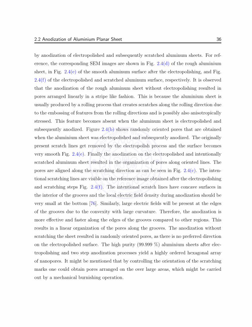
2.2 Anodization of Aluminium Planar Sheet 36
by anodization of electropolished and subsequently scratched aluminum sheets. For ref-
erence, the corresponding SEM images are shown in Fig. 2.4(d) of the rough aluminium
sheet, in Fig. 2.4(e) of the smooth aluminum surface after the electropolishing, and Fig.
2.4(f) of the electropolished and scratched aluminum surface, respectively. It is observed
that the anodization of the rough aluminum sheet without electropolishing resulted in
pores arranged linearly in a stripe like fashion. This is because the aluminium sheet is
usually produced by a rolling process that creates scratches along the rolling direction due
to the embossing of features from the rolling directions and is possibly also anisotropically
stressed. This feature becomes absent when the aluminum sheet is electropolished and
subsequently anodized. Figure 2.4(b) shows randomly oriented pores that are obtained
when the aluminium sheet was electropolished and subsequently anodized. The originally
present scratch lines get removed by the electropolish process and the surface becomes
very smooth Fig. 2.4(e). Finally the anodization on the electropolished and intentionally
scratched aluminum sheet resulted in the organization of pores along oriented lines. The
pores are aligned along the scratching direction as can be seen in Fig. 2.4(c). The inten-
tional scratching lines are visible on the reference image obtained after the electropolishing
and scratching steps Fig. 2.4(f). The intentional scratch lines have concave surfaces in
the interior of the grooves and the local electric field density during anodization should be
very small at the bottom [76]. Similarly, large electric fields will be present at the edges
of the grooves due to the convexity with large curvature. Therefore, the anodization is
more effective and faster along the edges of the grooves compared to other regions. This
results in a linear organization of the pores along the grooves. The anodization without
scratching the sheet resulted in randomly oriented pores, as there is no preferred direction
on the electropolished surface. The high purity (99.999 %) aluminium sheets after elec-
tropolishing and two step anodization processes yield a highly ordered hexagonal array
of nanopores. It might be mentioned that by controlling the orientation of the scratching
marks one could obtain pores arranged on the over large areas, which might be carried
out by a mechanical burnishing operation.

2.3 Anodization of Aluminium Microwire 37
2.3 Anodization of Aluminium Microwire
2.3.1 Anodization
The aluminium microwire was directly anodized using the two step anodization method.
There was no holder used and we directly suspended the aluminium microwire into the
solution. At the solution-air interface, we painted the microwire with lacquer to protect
the aluminium from the fast reaction at the interface. Otherwise, portion of microwire at
solution-air interface get complete anodization very fast and stop the electrical contact
to anodize the immersed portion of the microwire. A schematic of anodization setup has
been shown in Fig. 2.5. Aluminium microwires of 99.999% purity, and diameters 100
µm and 250 µm were purchased from Alfa Aesar company. The aluminium wires were
cleaned in acetone prior to the vacuum annealing at 500 C for three hours to increase
the grain size. The annealed wires were anodized in 0.3 oxalic acid solution made in DI
water. A tantalum (Ta) plate was used as the cathode. The system temperature was kept
at 0 C using an ice bath. Here we did not stir the solution because the wires were thin
and a small flow or turbulence could deform them. The first anodization time was kept
to be 30 minutes. After the first anodization, the alumina was etched away as in the case
of the aluminium planar sheet anodization. Second anodization was performed at the
same physical parameters as was done for the first anodization. The aluminium core from
the anodized wire was removed in the aluminium etching solution as was for the plane
sheet anodization. After the aluminium core removal, we obtained a hollow cylinder of
nanoporous alumina (cylindrical shell). Here 5% phosphoric acid used to carry out the
pore widening of the anodized wires.
2.3.2 Structural Characterization
A schematic picture of the anodized microwire is shown in Fig. 2.6, while the FESEM im-
ages of the obtained nanoporous alumina microtubes are shown in Fig. 2.7. If the surface

2.3 Anodization of Aluminium Microwire 38
DC Power Supply (40 V)
+ -
Thermal isolating jacket
Ice bath
Ta plate
Al micro wire
0.3 M H2C2O4
Lacquer
Figure 2.5: A schematic of the anodization setup to anodize the aluminium microwire.

2.3 Anodization of Aluminium Microwire 39
(a)
2 R1
2 R2
Al2O3Nanopore
Anodization
Nanopore
Al wire Anodized
Outer surface
wire
(b)
(c) (d)
Figure 2.6: Schematic of the structure of the cylindrical nanoporous alumina. (a)anodizing aluminium microwire, (b) outer surface of the anodized wire, (c) the transversecross section of the anodized wire and (d) the longitudinal cross section of the anodizedwire.

2.3 Anodization of Aluminium Microwire 40
(a) (b)
(c) (d)
(e) (f)
Figure 2.7: FESEM images of (a) electropolished aluminium wire, (b) anodized wire, (c)outer surface of the anodized wire, (d) transverse cross section of the anodized wire. Im-ages (e) and (f) are of hollow nanoporous alumina microtubes of small and large diameterrespectively.
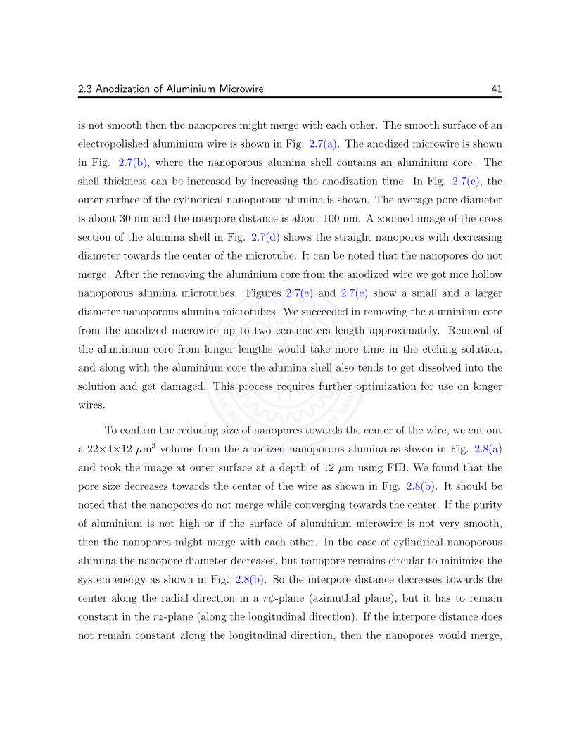
2.3 Anodization of Aluminium Microwire 41
is not smooth then the nanopores might merge with each other. The smooth surface of an
electropolished aluminium wire is shown in Fig. 2.7(a). The anodized microwire is shown
in Fig. 2.7(b), where the nanoporous alumina shell contains an aluminium core. The
shell thickness can be increased by increasing the anodization time. In Fig. 2.7(c), the
outer surface of the cylindrical nanoporous alumina is shown. The average pore diameter
is about 30 nm and the interpore distance is about 100 nm. A zoomed image of the cross
section of the alumina shell in Fig. 2.7(d) shows the straight nanopores with decreasing
diameter towards the center of the microtube. It can be noted that the nanopores do not
merge. After the removing the aluminium core from the anodized wire we got nice hollow
nanoporous alumina microtubes. Figures 2.7(e) and 2.7(e) show a small and a larger
diameter nanoporous alumina microtubes. We succeeded in removing the aluminium core
from the anodized microwire up to two centimeters length approximately. Removal of
the aluminium core from longer lengths would take more time in the etching solution,
and along with the aluminium core the alumina shell also tends to get dissolved into the
solution and get damaged. This process requires further optimization for use on longer
wires.
To confirm the reducing size of nanopores towards the center of the wire, we cut out
a 22×4×12 µm3 volume from the anodized nanoporous alumina as shwon in Fig. 2.8(a)
and took the image at outer surface at a depth of 12 µm using FIB. We found that the
pore size decreases towards the center of the wire as shown in Fig. 2.8(b). It should be
noted that the nanopores do not merge while converging towards the center. If the purity
of aluminium is not high or if the surface of aluminium microwire is not very smooth,
then the nanopores might merge with each other. In the case of cylindrical nanoporous
alumina the nanopore diameter decreases, but nanopore remains circular to minimize the
system energy as shown in Fig. 2.8(b). So the interpore distance decreases towards the
center along the radial direction in a rφ-plane (azimuthal plane), but it has to remain
constant in the rz-plane (along the longitudinal direction). If the interpore distance does
not remain constant along the longitudinal direction, then the nanopores would merge,

2.3 Anodization of Aluminium Microwire 42
(a) (b)
Figure 2.8: (a) An schematic to mill out the part of the cylindrical nanoporous aluminato see the pore size with respect to radius of the wire and (b) corresponding the FESEMimages of the milled out cylindrical nanoporous alumina.
which does not happen. This new feature of changing density of the nanopores makes the
cylindrical nanoporous alumina structurally inhomogeneous as well as anisotropic. We
had noted in the case of planar nanoporous alumina that the nanopore size remains con-
stant throughout the volume and comparatively, the planar nanoporous alumina system
is a homogeneous but anisotropic system. In later chapters, we shall model the optical
properties of the cylindrical nanoporous alumina system where the structural anisotropy
and inhomogeneity play a major role.
2.3.3 Effect of Radius of Curvature: Anodization Current andCrack Formation
We noted that during anodization of aluminium microwires, there was a crack can develop
in the nanoporous alumina shell after some time. There was usually no crack in the
planar nanoporous alumina sheet unlike this. We recorded the anodization current of
aluminium microwires of diameters 50 µm, 100 µm, 220 µm, and an aluminium sheet.
The recorded anodizations currents are shown in Fig. 2.9. The anodization current of

2.3 Anodization of Aluminium Microwire 43
aluminium microwires first increases quickly to a peak value and then decreases over
time. While decreasing, a sudden small jump occurs in the anodization current beyond
the peak value after some time and anodization current then decreases again. The time
of jump in the anodization current of the microwires of diameters 50 µm, 100 µm and 220
µm were around 60 minutes, 70 minutes and 110 minutes respectively which can be seen
in Figs. 2.9(a), 2.9(b) and 2.9(c) respectively (marked by the arrows). In comparision,
the anodization current of the aluminium sheet after the peak value always decreases
over time [63, 64, 77] and here there is no jump in the anodization current as shown
in Fig. 2.9(d). This jump in the microwire anodization current occurs because of the
formation of microcrack. When the crack occurs the effective resistivity between solution
and aluminium microwire decreases and the anodization current slightly increases. For
larger diameters of the microwires, the time at which the current changes rapidly shifted
towards longer times. For the planar aluminium sheet the radius of curvature is effectively
infinite and the anodization current remains steadily decreasing with no sudden changes.
In Figs. 2.10, two anodized wires of the same diameter have shown. Figure 2.10(a)
is for 30 minutes anodization and there is no crack in the microtube. Figure 2.10(b)
is for 70 minutes anodization, when sample had been taken out just after the jump in
the anodization current occurred. We see that there a small crack in the nanoporous
alumina shell. If the aluminium microwire is anodized for longer time, then the crack size
also becomes larger. We know that the anodization starts perpendicular to the planar
aluminium sheet surface and there is a volume expansion, as the volume of nanoporous
alumina is much larger compared to the original volume of the aluminium [44]. In the case
of the planar aluminium sheet anodization, the reactive area of aluminium always remains
constant throughout the anodization while the volume of nanoporous alumina increases
perpendicular to the sheet surface. So the cracks do not occur in the planar nanoporous
alumina because its reactive area is always constant. In the case of anodization of the
aluminium microwire the anodization starts perpendicular to the curved surface along
the radial direction towards the center in the cylindrical symmetry. So the effective

2.3 Anodization of Aluminium Microwire 44
reactive area continuously decreases with radius and the relative volume expansion of
the nanoporous alumina increases. Thus, the alumina is under tensile stress and also
plastically deforms to some extent. Eventually with continued stress building up, a crack
suddenly appears as the yield point is crossed. For the smaller diameter of the microwire
the effective reactive area decreases faster compared to the larger diameter microwire, so
the crack formation occurs earlier for microwires with smaller diameter.
2.3.4 Effect of Radius of Curvature: Organization of nanoporesand Shell Thickness
To see the effects of the radius of curvature of the wire on the pore size, interpore distance
and shell thickness, we anodized two different diameters wires, one of 25 µm and other 230
µm, for the same time. We observe that in both the anodized wires, the average nanopore
size is 30 mn and the interpore distance is 100 nm at the outer surface, while there is
difference in the nanoporous alumina shell thickness. For smaller diameter of the wire,
the shell thickness was less than the shell thickness of the larger diameter wire. Figures
2.11(a) and 2.11(b) show the cross sections of the large 230 µm diameter anodized wire,
and Figs. 2.11(c) and 2.11(d) show the cross section and outer surface of the anodized
wire of diameter 25 µm.
Just after the anodization, for fixed anodization parameters, the pore diameters
and interpore distance at outer surface remain constant for smaller and larger diameters
microwires both. But the nanopores diameter can be increased by pore widening upto
just lesser than the interpore distance. These two quantities, nanopore diameter and
interpore distance towards the center along the radial direction vary faster with radius
for smaller diameter microwires compare to larger diameter microwires. These quantities
can be changed by changing the acid or the anodization parameters or both. In the same
anodization time, the nanoporous alumina shell thickness is lesser for smaller diameter
microwire compared to larger diameter microwire because the effective reactive area de-

2.3 Anodization of Aluminium Microwire 45
(a) (b)
(c) (d)
Figure 2.9: The measured anodization current of aluminium microwires of diameters(a) 50 µm, (b) 100 µm and (c) 220 µm. The small jump in the anodization current ofanodization of aluminium microwires of (a), (b) and (c) occurred around 60 minutes, 70minutes and 110 minutes respectively. (d) The anodization current of an aluminium sheetfor reference. There is no jump in the anodization current of aluminium sheet anodization.

2.3 Anodization of Aluminium Microwire 46
(a) (b)
Figure 2.10: FESEM images of anodized wire to show the crack formation in thenanoporous shell while anodization. (a) No crack for 30 min anodization and (b) samplejust after the crack take place. The anodization time was 70 min.
creases faster. As the radius of curvature of microwire increases, the rate of change of the
reactive area decreases and tends to zero value for infinite radius of curvature.
2.3.5 Optical Transparency of Nanoporous Alumina Microtubes
The alumina are transparent in the visible range. The nanoporous alumina are structured
materials. To see the transparency of the nanoporous alumina shell, we took the optical
reflection images of an electropolished aluminum microwire and a nanoporous alumina
tube with an optical microscope (Olympus BX51). The optical reflection images of the
aluminium microwire and the nanoporous alumina tube with a hollow core are shown
in Figs. 2.12(a) and 2.12(b) respectively. We see that the light is highly reflected from
the electropolished surface of the wire, while the nanoporous alumina tube is optically
transparent. The air core is visible at the center in the microtube. Since these are
transparent, therefore, the cylindrical nanoporous alumina with or without aluminium
cores can be used as optical waveguides. The presence of a few surface inhomogeneities
as well as some scattering enter in the nanopores alumina microtube can be seen. In
the later chapters we shall discuss the optical waveguide properties of these cylindrical

2.3 Anodization of Aluminium Microwire 47
(a) (b)
(c) (d)
Figure 2.11: FESEM images of anodized wire to show the curvature effect on thenanopore size and interpore distance. (a) and (b) for large diameter, and (c) and (d)for small diameter.

2.4 Metalization of Nanoporous Alumina 48
(a) (b)
Figure 2.12: Optical microscope images in reflection mode of (a) an electropolishedaluminium wire and (b) anodized wire with hollow core.
nanoporous alumina for optical and infrared frequencies.
2.4 Metalization of Nanoporous Alumina
There are various kinds of materials such metals, oxides, polymers that can be deposited
into the pores of the planar nanoporous alumina [28, 46, 71, 78]. Metalized nanoporous
alumina have become very interesting to the scientific community after the development
of the metamaterials [28, 78]. Several metals can be electrodeposited in the nanopores of
the nanoporous alumina making it a popular template. This represents a readymade form
of anisotropic or hyperbolic metamaterials. Among the metals, silver is highly preferred
because of its plasmonic properties and less lossy nature. All the depositions so far
have been made in planar nanoporous alumina templates, and growth of nanowires in
cylindrical nanoporous alumina is not reported yet. In the next subsection, we present
the deposition of silver nanowires deposition in planar nanoporous alumina, and in the
subsequent subsection, in cylindrical nanoporous alumina microwires.

2.4 Metalization of Nanoporous Alumina 49
2.4.1 Nanowire Deposition into Planar Nanoporous Alumina
The electrodeposition is carried out with silver metal. After etching the aluminium from
the anodized samples, the alumina template was immersed in 5% phosphoric acid at room
temperature for 90 minutes to remove the barrier layer. During the barrier layer removal
the nanopores were also widened by the acid. The front side of the template was coated
with 160 nm gold film as a seed layer. As shown in Fig. 2.13(a) the gold coated template
was kept on an aluminium foil and the all back and sides were covered with scotch tape.
The gold coated templates were used as the cathode and a platinum wire as the anode.
0.2 M silver nitrate (AgNO3) solution maintained in an ice bath was used as electrolyte
to deposit the silver nanowires. Putting both the electrodes in the silver nitrate solution,
a 30 mA current was passed for 40 minutes to electrodeposit the silver nanowires into
the alumina templates. After the deposition, the scotch tape was removed for further
characterization.
The Fig. 2.13(b) show the FESEM image of electrodeposited silver nanowires into
the planar nanoporous alumina. The white dotted area of Fig. 2.13(b) is zoomed out Fig.
2.13(c). We can clearly see that the silver nanowires are deposited into the nanopores
of the planar nanoporous alumina. The nanowires deposited in the pores of planar
nanoporous alumina are broken at several places. Possibly there may be two reasons
for broken nanowires. The first reason could be due to the lack of proper electrical con-
tact between the gold thin film and the aluminium foil and the second reason is that we
used the silver nitrate water solution only and we have not mixed any surfactant etc. to
control the wettability of the system.
2.4.2 Nanowire Deposition into Cylindrical Nanoporous Alu-mina
The situation of cylindrical nanoporous alumina is quite different than the planar nanoporous
alumina. Because the diameter of the cylindrical nanoporous alumina is sub-hundred mi-
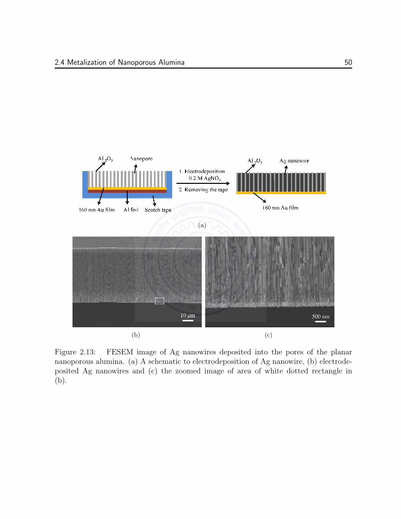
2.4 Metalization of Nanoporous Alumina 50
(a)
(b) (c)
Figure 2.13: FESEM image of Ag nanowires deposited into the pores of the planarnanoporous alumina. (a) A schematic to electrodeposition of Ag nanowire, (b) electrode-posited Ag nanowires and (c) the zoomed image of area of white dotted rectangle in(b).

2.4 Metalization of Nanoporous Alumina 51
crometer in size and we can not easily make a seed gold layer on the inner side of the
template. But we have an aluminium core which can be utilized as a conducting electrode.
To remove the barrier layer of impermeable alumina inside the cylindrical nanoporus alu-
mina, the voltage after anodization was reduced slowly to zero. We reduced the voltage
in steps of 5 V from 40 V to 5 V. After each voltage reducing step, 5 minutes was al-
lowed to stabilize the anodization current. From 5 V to 0 V, we reduced the potential
in steps of 1 V/min. After the anodization was completed, the templates were immersed
in 5% phosphoric acid for half hour to remove the barrier layer completely. This process
widened the nanopores size as well to some extent. The barrier layer removed cylindrical
nanoporous alumina with aluminium core was used as the cathode and a platimum wire
used as the anode. Both the electrodes were immersed in an ice cold electrolyte which
was mixture of AgNO3(3.5gm.), CH3COONH4(2.8 gm.), NH3H2O (25 % extra pure) (4.61
ml.) in 70 ml of solution [68]. A 3 mA current was applied for 40 minutes to deposit the
silver nanowires.
Figure 2.14(a) shows a schematic of electrodeposited silver nanowires in the cylindri-
cal nanoporous alumina. The silver nanowires are embedded in the alumina matrix. The
FESEM image of the silver nanowires in cylindrical nanoporous alumina is shown in Fig.
2.14(b). This FESEM image is taken at the position white dotted area in Fig. 2.14(a). We
see that there is an aluminium core and it is surrounded by the metal filled nanoporous
alumina shell. The Fig. 2.14(c) is the zoomed image of Fig. 2.14(b) within the white
dotted area. The presence of the silver nanowires were confirmed by the Energy-dispersive
X-ray spectroscopy (EDX) as shown in Fig. 2.14(d).
We have thus succeeded in electrodepositing the silver nanowires into a very thin
layer of the nanoporous alumina shell, where the shell thickness is small compared to
the diameter of the aluminium wire. The reason is that as the shell thickness increases,
the nanopore size decreases towards the center and it becomes very difficult to remove
the barrier layer. In future, some other methods might prove successful to remove the
barrier layer from the much thicker nanoporous alumina shell. Using the other method

2.4 Metalization of Nanoporous Alumina 52
(a) (b)
(c)
Project 1 1/19/2015 1:18:05 PM
Comment:
Spectrum processing :
No peaks omitted
Processing option : All elements analyzed (Normalised)
Number of iterations = 3
Standard :
O SiO2 1‐Jun‐1999 12:00 AM
Al Al2O3 1‐Jun‐1999 12:00 AM
Ag Ag 1‐Jun‐1999 12:00 AM
Element Weight% Atomic%
O K 24.11 50.28
Al K 28.31 35.00
Ag L 47.58 14.72
Totals 100.00
(d)
Figure 2.14: FESEM image of Ag nanowire deposited in the cylindrical nanoporousalumina. (a) A schematic to electrodeposition of Ag nanowire, (b) electrodeposited Agnanowires. The white dotted rectangle position of (a) is shown in (b), (c) the zoomedimage of area of white dotted rectangle in (b) and the EDX spectra of Ag nanowireembedded in nanoporous alumina shell.

2.5 Conclusions 53
for barrier layer removal and electrodeposition would require further work to optimize the
procedures.
2.5 Conclusions
We investigated some new features of the anodization of the aluminium microwires of
circular cross section. In planar nanoporous alumina, the nanopores size remain uniform
throughout the volume, and the system is homogeneous and anisotropic. In cylindrical
nanoporous alumina, in comparison with planar nanoporous alumina, the nanopore sizes
decrease towards the axis of the microwire. The azimuthal interpore distance decreases
towards the wire axis while the longitudinal interpore distance remains constant. This
cylindrical nanoporous alumina system is both inhomogeneous and anisotropic. After re-
moving the aluminum core by etching, the hollow nanoporous alumina microtubes could
be obtained. The nanoporous alumina microtubes are optically transparent. The alu-
minium core could only be removed from a small lengths ( 2-3 cm) of the anodized wire
as the alumina also dissolves while removing the aluminium core from longer lengths of
the anodized wire. For longer times of anodization, there were cracks that form in the
nanoporous alumina shell because of the volume expansion, and which could be detected
by a sudden increase in the anodization current. The time at which the crack occurs
for the first time increases with the radius of the microwire, and it is indefinitely long
for a plane sheet. For fixed anodization parameters, the shell thickness would be lesser
for smaller wire diameters while the nanopores size and the interpore distance remains
constant at the outer surface. The nanopore size can be increased nearly to the interpore
distance by pore widening process. The barrier layer of the cylindrical nanoporous alu-
mina was removed by the voltage reduction method, and the aluminium core remains at
the center. The electrodeposition of the silver nanowires within the pores of the planar
nanoporous alumina could be carried out to obtain very thick nanoporous alumina tem-
plates, while for sub-hundred micrometer diameter size cylindrical nanoporous alumina,

2.5 Conclusions 54
the electrodeposition was not possible for much thicker shells because of the decreasing
size of nanopores towards the center and the consequent difficulty in the removal of the
insulating barrier alumina layer.

Chapter 3
Homogenized Material Parametersof Cylindrical Nanoporous Alumina
3.1 Introduction
In chapter 2, we have described the fabrication of planar nanoporous alumina and cylin-
drical nanoporous alumina microtubes. We have also shown that incorporation of metallic
nanorods is possible within the pores in the planar as well as cylindrical nanoporous alu-
mina. To understand wave propagation in the nanoporous alumina, we need to model
its material parameters by considering it as a homogeneous medium using some valid
homogenization method. To homogenize a composite medium, the inclusions should be
electrically small, that is, the size of the dispersed particles must be much smaller than
the wavelength [7, 79]. The homogenization of planar nanoporous alumina is well known
in the literature [51, 80, 81], but the homogenization of cylindrical nanoporous alumina
has not been reported.
The Bruggemann homogenization [7,79,82] and Maxwell-Garnett homogenization [7,
79, 83] are widely used two methods for the homogenization of binary mixtures. Since
in our case the fill fraction of the inclusion can be made small and the Maxwell-Garnett
homogenization works well for fill fraction less than 0.3 [84, 85], therefore, we shall use
55

3.2 Homogenization of Planar Nanoporous Alumina 56
(a) (b)
Figure 3.1: The schematic of (a) planar nanoporous alumina where the nanopores areorganized in hexagonal pattern in xy−plane and oriented uniformally along z−direction,and (b) the top surface area of the planar nanoporous alumina showing a unit shell.
the latter method to homogenize the nanoporous alumina system. In the second section,
we homogenize the planar nanoporous alumina.
In the cylindrical nanoporous alumina, the diameter of the nanopores decrease to-
wards the center of the cylinder, hence only a local homogenization will be possible. In
the third section we describe the structural parameters of the cylindrical nanoporus alu-
mina required for modeling the effective medium. In the fourth section, we transform
the cylindrical geometry into a plane geometry using the technique of transformation op-
tics [16, 86, 87]. We have homogenized the cylindrical nanoporous alumina microtubes in
the new transformed geometry and then after homogenization we invert the transforma-
tion to obtain the material parameters in the original geometry [88].

3.2 Homogenization of Planar Nanoporous Alumina 57
3.2 Homogenization of Planar Nanoporous Alumina
Figure 3.1 shows a schematic picture of planar nanoporous alumina. The nanopores have
hexagonal arrangement in the xy-plane and are oriented along the z-direction as shown in
Fig. 3.1(a). The nanopores are uniformly distributed in the whole volume. Figure 3.1(b)
shows the unit cell in the xy-plane. Let the nanopore diameter and interpore distance
be 2Q and D(= dy) respectively. Then the nanopore fill fraction f can be given by the
following expression
f =Area of nanopores within unit cell
Area of unit cell(3.1a)
=2× (πQ2)(√
3D)×D
(3.1b)
=2πQ2
√3D2
(3.1c)
Here the nanopore fill fraction is same everywhere in the volume. It only depends
on the nanopore diameter and the interpore distance. For a fixed interpore distance,
the nanopore fill fraction can be changed by increasing the nanopore diameters by pore
widening process described in Chapter 1.
For the present, let us assume that the nanopores of planar nanoporous alumina are
filled with a material that has a dielectric permittivity of εi. Since the nanopores have very
high aspect ratio, therefore, the polarizability along the nanowires direction is effectively
zero while there is finite polarizability in the transverse direction of the nanopores. The
effective permittivity of the planar nanoporous alumina along the nanopores direction,
εz, can be approximately given by the volume average as [89,90]
εz = fεi + (1− f)εh (3.2)
where εi and εh are the permittivities of inclusion (air or metal) and host (alumina)
respectively.

3.3 Structural Modeling of Cylindrical Nanoporous Alumina 58
Since we are considering the areal (area/area) fill fraction, therefore, the effective
permittivties εx and εy along the x-direction and y-direction will be equivalent, that is,
εx = εy. The effective permittivity along the transverse direction can be obtained by the
Maxwell-Garnett homogenization (MGH) theory, and for the cylindrical inclusion it can
be given by the following expression [90]
εx = εy =(1 + f)εiεh + (1− f)ε2
h
(1− f)εi + (1 + f)εh. (3.3)
The Eqs. (3.2) and (3.3) are approximate results and work well for the smaller (< 0.3)
fill fractions. They can not, however, be used for larger fill fractions accurately.
3.3 Structural Modeling of Cylindrical Nanoporous
Alumina
A cylindrical nanoporous alumina shell whose inner and outer radii are R1 and R2 is
shown in Fig. 3.2. We divide the cylindrical nanoporous alumina system into three
regions. Region-I: inner core from cylindrical axis to R1 may be metallic or dielectric.
Region-II: consisting of the nanoporous alumina shell from R1 to R2; Region-III: the
outermost region beyond R2 which may be metal or dielectric. We assume that at the
outer surface of the cylindrical nanoporous alumina (r = R2), the nanopores organization
is ideally hexagonal packed as shown in Fig. 3.2(a). The interpore distances decrease
along the azimuthal direction and there is no change in the interpore distance along the
z-direction towards the cylindrical axis. Let the interpore distance be D2 at R2 and the
nanopore diameter be 2Q2 there. Let the interpore distance be d at the φz-surface at
radius r, and the nanopore diameter be 2q at that point. Consider the unit cell as shown
in Fig. 3.2(b). The solid angle Ω made by the surface area of the pore at R2 and r will
be same. Therefore, at a point in the nanoporous alumina shell at a distance r from the

3.3 Structural Modeling of Cylindrical Nanoporous Alumina 59
(a) (b)
Figure 3.2: The schematic of (a) position a cylindrical shell of radius r and (b) a smalllocal area on the general φz surface at radius r.
center axis,
Ω(r) = Ω(R2), (3.4a)
πq2
r2=πQ2
R22
, (3.4b)
q =Q2
R2
r. (3.4c)
Equation (3.4c) shows that the pore radius linearly depends on the radial distance from
the center of the microwire.
If the pore periodicity at R2 is D2, then from the Fig. 3.2(b) the unit cell length
along φ-direction and along z-direction
d2,φ =√
3D2, (3.5a)
d2,z = D2. (3.5b)
In the azimuthal plane, the angular width of the unit cell at R2
∆φ =
√3D2
R2
. (3.6)
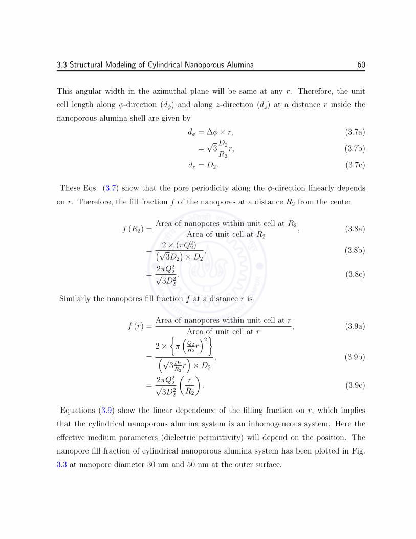
3.3 Structural Modeling of Cylindrical Nanoporous Alumina 60
This angular width in the azimuthal plane will be same at any r. Therefore, the unit
cell length along φ-direction (dφ) and along z-direction (dz) at a distance r inside the
nanoporous alumina shell are given by
dφ = ∆φ× r, (3.7a)
=√
3D2
R2
r, (3.7b)
dz = D2. (3.7c)
These Eqs. (3.7) show that the pore periodicity along the φ-direction linearly depends
on r. Therefore, the fill fraction f of the nanopores at a distance R2 from the center
f (R2) =Area of nanopores within unit cell at R2
Area of unit cell at R2
, (3.8a)
=2× (πQ2
2)(√3D2
)×D2
, (3.8b)
=2πQ2
2√3D2
2
. (3.8c)
Similarly the nanopores fill fraction f at a distance r is
f (r) =Area of nanopores within unit cell at r
Area of unit cell at r, (3.9a)
=
2×π(Q2
R2r)2
(√3D2
R2r)×D2
, (3.9b)
=2πQ2
2√3D2
2
(r
R2
). (3.9c)
Equations (3.9) show the linear dependence of the filling fraction on r, which implies
that the cylindrical nanoporous alumina system is an inhomogeneous system. Here the
effective medium parameters (dielectric permittivity) will depend on the position. The
nanopore fill fraction of cylindrical nanoporous alumina system has been plotted in Fig.
3.3 at nanopore diameter 30 nm and 50 nm at the outer surface.

3.4 Geometric Transformation using Transformation Optics 61
Figure 3.3: Nanopores fill fraction of cylindrical nanoporous alumina when nanoporediameters are 30 nm and 50 nm at the outer surface.
3.4 Geometric Transformation using Transformation
Optics
The ad-hoc homogenization of the nanoporous alumina microtube have several assump-
tions such as the inhomogeneity could be disregarded to locally homogenize the system
at different radial distances. In this section, we shall carry out the homogenization rig-
orously using the techniques of transformation optics [86, 91]. Using a mapping we show
that an effective anisotropic dielectric tensor can be obtained for the medium with radially
oriented nanowires/nanopores in the curvilinear geometry as well.
The cylindrical shell can be transformed into a rectangular slab by the transforma-
tion into cylindrical coordinates,
x = ln r, y = φ, z = z. (3.10)
In the new coordinate frame (x, y, z), the transformed material parameters and fields can
be written as [91]
εj = εjS1S2S3
S2j
, µj = µjS1S2S3
S2j
, Ej = SjEj, Hj = SjHj, (3.11)

3.4 Geometric Transformation using Transformation Optics 62
Figure 3.4: A cylindrical shell is mapped to a flat slab. The nanopores along the radialdirection in shell mapped along the x-direction in the new frame.
S2j =
(∂r
∂qj
)2
+
(r∂φ
∂qj
)2
+
(∂z
∂qj
)2
, (3.12)
where tilde (˜) represents the new transformed frame. Now using Eqs. (3.10)–(3.12), the
material parameters in the new frame for the embedded material (i) and alumina host
material (h) within their respective regions are given by
εx,i = εr,i, εy,i = εφ,i, εz,i = e2xεz,i, (3.13a)
µx,i = µr,i, µy,i = µφ,i, µz,i = e2xµz,i, (3.13b)
εx,h = εr,h, εy,h = εφ,h, εz,h = e2xεz,h, (3.13c)
µx,h = µr,h, µy,h = µφ,h, µz,h = e2xµz,h. (3.13d)
In this manner, we can transform the cylindrical shell with radially emanating nanopores/nanorods
into a slab with columns along the x direction (see Fig. 3.4). The only difference from
a medium of unidirectional nano-columns is that both the background material of the
slab and the columns are now both anisotropic and inhomogenous (along z) in the new
geometry. Such a structure can be easily homogenized by noting that the principal axis
of anisotropy coincides with the column axes and the fact that we have only diagonal
anisotropy.

3.5 Homozenization of Cylindrical Nanoporous Alumina 63
3.5 Homozenization of Cylindrical Nanoporous Alu-
mina
Now we will proceed to homogenize the structure in the new geometry, and then transform
the obtained effective-medium parameters back to the cylindrical geometry. This will be
valid at all points, except at the origin in the cylindrical geometry where there is a
singularity, which is excluded in the homogenization. The effective permittivity along the
x-direction with the help of Eq. (3.13) can be given by the volume average [89,90]
εeffx = fεr,i + (1− f)εr,h, (3.14)
where f is the fill fraction of the inclusion. In the transverse direction, the effective
permittivity can be approximately obtained by the Maxwell-Garnett homogenization
procedure. We would need the polarizabilities of anisotropic cylinders embedded in an
anisotropic medium. The polarisability of an anisotropic prolate spheroid in an isotropic
medium is well known [92] and the homogenization of anisotropic ellipsoids embedded in
an anisotropic medium has been also been obtained [93].
The coincidence of the principal axes of anisotropy with the symmetry axes of the
geometry makes it simple here. In our case, as the inclusion is cylindrical with very
large aspect ratio, therefore, it can be approximated as a prolate spheroid with extreme
eccentricity (like a long needle). The normalized electric field of an anisotropic cylinder
with ¯ε = (1, 1, r20) embedded in an anisotropic medium ¯ε = (εAl2O3 , εAl2O3 , εAl2O3r
20) which
is placed in a uniform electric field have been plotted using COMSOL Multiphysics is
shown in Fig. 3.5(a). Here εAl2O3 (= 2.6375) is the dielectric permittivity of the isotropic
alumina and r0 (= 12.5µm) is the outer radius of cylindrical shell. The field plot of
an anisotropic nanowire with ¯ε = (εAg, εAg, εAgr20) embedded in an anisotropic medium
¯ε = (εAl2O3 , εAl2O3 , εAl2O3r20) is shown in Fig. 3.5(b), where εAg (= −1359.1400+i115.5060)
represents the dielectric permittivity of silver metal. For comparison the field plots of an
isotropic air cylinder with ε = 1 and an isotropic silver cylinder with εAg = −1359.1400 +

3.5 Homozenization of Cylindrical Nanoporous Alumina 64
i115.5060 placed in isotropic alumina εAl2O3 = 2.6375 are shown in Fig. 3.5(c) and 3.5(d)
respectively. Since the diameter of anisotropic cylinder with ¯ε = (1, 1, r20) and anisotropic
nanowire with ¯ε = (εAg, εAg, εAgr20) both are electrically small, therefor, the field plots
are almost look like the case of isotropic air cylinder and isotropic silver nanowire. We
see that the field plots for anisotropic cylinders are almost the same as the field plots of
the isotropic cylinders as well as the polarizability. So the local homogenization is good
approximation for such type of system. The homogenized effective-medium parameters
are obtained as [90]
εeffy =
(1 + f)εφ,iεφ,h + (1− f)ε2φ,h
(1− f)εφ,i + (1 + f)εφ,h, (3.15)
and
εeffz = e2x
(1 + f)εz,iεz,h + (1− f)ε2z,h
(1− f)εz,i + (1 + f)εz,h. (3.16)
The additional exponential factor in the εeffz results in a biaxial and inhomogeneous
medium in the Cartesian coordinate frame of rectangular slab. Thus, it is different from
a flat nanoporous anodic alumina template.
Now we will map back these parameters into the original cylindrical geometry and
obtain
εeffr = fεr,i + (1− f)εr,h, (3.17)
εeffφ =
(1 + f)εφ,iεφ,h + (1− f)ε2φ,h
(1− f)εφ,i + (1 + f)εφ,h, (3.18)
and
εeffz =
(1 + f)εz,iεz,h + (1− f)ε2z,h
(1− f)εz,i + (1 + f)εz,h. (3.19)
Note that the exponential factors of e2x cancel in the inverse mapping process. Since
in the cylindrical geometry, the individual materials are isotropic, the effective permit-
tivity components εeffφ and εeff
z are equal in this approximation. Incidentally, we obtain
an identical result as obtained by just applying this process directly in the curvilinear

3.5 Homozenization of Cylindrical Nanoporous Alumina 65
(a) (b)
(c) (d)
Figure 3.5: The COMSOL calculated, the normalized electric field of (a) anisotropiccylinder with ¯ε = (1, 1, r2
0) in an anisotropic medium ¯ε = (εAl2O3 , εAl2O3 , εAl2O3r20),
(b) anisotropic cylinder with ¯ε = (εAg, εAg, εAgr20) in an anisotropic medium ¯ε =
(εAl2O3 , εAl2O3 , εAl2O3r20), (c) isotropic air cylinder with ε = 1 in an isotropic alumina
ε = εAl2O3 and (d) isotropic silver cylinder with ε = εAg in an isotropic alumina ε = εAl2O3 .The color shows the normalized electric field and the arrow show the electric field direc-tions. Here εAl2O3 = 2.6375, εAg = −1359.1400 + i115.5060 and r0 = 12.5µm.

3.5 Homozenization of Cylindrical Nanoporous Alumina 66
geometry. This is the due to the large aspect ratio of the inclusions and the electrically
small diameter of the nanopores aligned along the r-direction. We also note that cylindri-
cally symmetric metamaterials have been also been homogenized using similar geometric
transformations [94,95], including for the design of anisotropic invisibility cloaks [96].
In this picture, only the areal fill fraction (f) of the pore/nanorod determines the
effective medium properties and the anisotropy results in εr 6= εφ and εz ' εφ. From the
FESEM images of several samples, we find that the nanopore cross-section approximately
reduces linearly with the radial distance in alumina microtubes anodized at constant
voltage, and the areal fill fraction changes with the radial distance as Eq. 3.9. Typically,
D2 = 100 nm at the outer surface of the anodized aluminium wire where anodization
begins when an anodization voltage of 40 V is used at 0 C in oxalic acid (see Chapter
2). Similarly, the pore diameter 2Q2 is 30 nm under these circumstances. The pore
diameter can be flexibly increased to any any value up to about 90 nm by pore widening
in a solvent such as phosphoric acid. At a wavelength of 632.8 nm, Fig. 3.6 shows
the variation in the anisotropic material parameters with the radial distance obtained
for the cases of (i) air nanopores in nanoporous alumina and (ii) silver nanorods in the
nanoporous alumina, where a Drude dielectric permittivity for silver (Fig. 3.7(b)) was
used as εAg = ε∞ − ω2p/[ω(ω + iγ)] with ε∞ = 5.7, ωp = 9.2eV and γ = 0.021eV [8].
For the host alumina material (Fig. 3.7(a)), the dielectric permittivity have been taken
from [1]. The imaginary part of the effective medium parameters for the silver filled
nanoporous structure is also small due to the small fill fractions (0.23) of silver. Due to the
radial variation of the pore diameters, these fibers are actually spatially inhomogenous.
Typically, nanowires made of plasmonic materials that have Re(ε) < 0 results in an
extreme effective anisotropy with εr < 0 and εφ > 0.
At a constant nanopore fill fraction of 0.23, the effective permittivity components
with respect to the frequency have been plotted in Fig. 3.8. Here also the alumina data
is taken from Ref. [1] and the silver data is from Ref. [8]. For the case of air inclusions
as shown in Fig. 3.8(a), the permittivity components are anisotropic. The anisotropy is

3.5 Homozenization of Cylindrical Nanoporous Alumina 67
(a) (b)
(c) (d)
(e) (f)
(g) (h)
Figure 3.6: The effective permittivity components of cylindrical nanoporous alumina withrespect to the radius of the wire at 442 nm, 532 nm, 632.8 nm and 785 nm wavelengths.The left panel is for air inclusion and the right panel is for the silver inclusion.

3.5 Homozenization of Cylindrical Nanoporous Alumina 68
(a) (b)
Figure 3.7: The permittivity of (a) pure alumina (Weber, Handbook of Optical Ma-terials, 2003) and (b) silver metal of Drude model (Cai et al., Optical Metamaterials:Fundamentals and Applications, 2010).
larger for higher frequencies. The material dispersion for the case of silver inclusions is
shown in Fig. 3.8(b). The signs of εr and εφ vary over the given spectral range. We see
that in certain spectral range the permittivity components show the hyperbolic dispersion.
In the case of air inclusion, the εr is always greater than the εφ is shown in Fig. 3.8(a). If
we fill the nanopores of cylindrical nanoporous alumina with some higher index medium
compare to alumina then this inequality can be reversed, that is, in this case εr < εφ. But
if we fill the nanopores of the cylindrical nanoporous alumina with metals then all the
inequality exist. Figure 3.8(b) shows the effective permittivity components of cylindrical
nanoporous alumina with silver metal inclusion. It shows that below the 600 THz there
is indefinite permittivity with εr < 0, εφ > 0 which have very high metallic losses. In a
very narrow rage around 800 THz there is εr > 0, εφ < 0. But beyond this range there
is normal anisotropy. It is clear that the metal inclusion increases the anisotropy of the
nanoporous alumina.

3.5 Homozenization of Cylindrical Nanoporous Alumina 69
(a) (b)
(c) (d)
Figure 3.8: The effective permittivity components of cylindrical nanoporous aluminaat constant nanopore fill fractions of 0.08 and 0.23 with respect to the frequency. Theleft panel for air inclusion, and the right panel for silver inclusion. Here R1=0.5µm andR2=12.5µm.

3.6 Conclusions 70
3.6 Conclusions
We have carried out a homogenization analysis using the structural parameters of the
cylindrical nanoporous alumina microtubes. The nanopore diameter of nanopores, az-
imuthal interpore distance and the nanopore fill fraction vary linearly with the radius
of the wire. All these three decrease toward the microwire axis, and the cylindrical
nanoporous alumina is an inhomogeneous and anisotropic medium. These variations are
not available in the planar nanoporous alumina which is only an anisotropic but a homo-
geneous system. We locally homogenized the cylindrical nanoporous alumina using the
technique of the transformation optics and the Maxwell-Garnett homogenization theory.
We found that for the case of air inclusions the system has inhomogeneous and anisotropic
dispersion while for the silver inclusion the system has anisotropic as well as hyperbolic
dispersion depending on the electromagnetic spectral ranges. For fixed inclusions, these
dispersions can be changed by changing the nanopore diameters or changing the inter-
pore distance. For fixed nanopore diameters and interpore distance the dispersions can be
changed by using the different inclusions. This method is only valid for dilute inclusions
(f < 0.3). For higher fill fraction (f > 0.3), these homogenization would not be valid and
in that case we have to use some other homogenization method such as Bruggemann’s ho-
mogenization method. In the case of air inclusions there are less losses almost over whole
given range but there are huge losses for metallic inclusions in lower frequency ranges.

Chapter 4
Homogeneous, AnisotropicMetamaterial Optical Fiber
4.1 Introduction
Circular waveguides optical fibers have been studied since several decades [97]. They are
being used in many scientific and engineering applications such as communication, power
transmission, sensors, medical, instruments etc. Most of them are isotropic in nature
and light confinement is due to the total internal reflections. Later on photonic crystal
fibers, which are internally structured but invariant along the axial direction, have been
introduced [29]. In these fibers, few micrometer size holes placed in a perodic manner are
drawn along the fiber axis and light is guided by the photonic band gap in the transverse
direction [30]. Development of metamaterials has opened new doors for applications
of optical fibers [7]. Using metamaterials, any desired anisotropy can be introduced in
the waveguides and optical fibers [31, 53, 98]. The modal dispersions of an anisotropic
dielectric permittivity fiber have been recently discovered [36]. The light guiding nature
of metamaterial clad hollow waveguides also has been of interest, where the anisotropy in
the clad region is produced by the split ring resonators [39,40].
In the Chapter 2 we have discussed about the fabrication of radially structured
71

4.2 Electromagnetic Fields in a Cylindrically Symmetric Anisotropic Medium 72
microtubes of nanoporous alumina, whose effective parameters have been theoretically
found in Chapter 3 using the Maxwell-Garnett homogenization theory. In this chapter we
shall discuss about the wave guiding nature of these radially structured fibers. These fibers
have an anisotropy with cylindrical symmetry that renders the polarization in the axial,
radial and azimuthal directions different. To simplify the discussion, we shall consider that
the anisotropic medium is homogeneous in this chapter. This assumption will be relaxed
in the next chapter. We find these waveguides to support novel modes, particularly where
the anisotropy is indefinite and the mode dispersions become hyperbolic. The new modes
possible are analyzed and explained in this chapter. Conditions for the guidance are also
analyzed.
4.2 Electromagnetic Fields in a Cylindrically Sym-
metric Anisotropic Medium
Consider a cylindrically symmetric medium with anisotropy along the radial, azimuthal
and axial directions as given by the homogenization in Chapter 3 for a nanoporous alumina
microtube. More generally, both the dielectric permittivity (¯ε) and magnetic permeability
(¯µ) can be anisotropic and are second ranked tensors that can be represented by 3 × 3
matrices. For cylindrically symmetric anisotropic medium for diagonal anisotropy, ¯ε and
¯µ are given as
¯ε =
εr 0 00 εφ 00 0 εz
, (4.1a)
¯µ =
µr 0 00 µφ 00 0 µz
. (4.1b)
The medium for the present discussion (in this chapter) will be regarded as homogeneous.
The Maxwell’s equations for time harmonic electromagnetic fields in a source free, linear,
anisotropic and homogeneous medium can be written as

4.2 Electromagnetic Fields in a Cylindrically Symmetric Anisotropic Medium 73
~∇ ·(ε0 ¯ε ~E
)= 0, (4.2a)
~∇ ·(µ0 ¯µ ~H
)= 0, (4.2b)
~∇× ~E = iωµ0 ¯µ ~H, (4.2c)
~∇× ~H = −iωε0 ¯ε ~E. (4.2d)
We are interested in guided mode solutions in the waveguide that propagate along the
waveguide axis (z-direction). Hence, we consider the form of electromagnetic wave prop-
agating in the fiber as
~E (r, φ, z, t) = ~E (r, φ) ei(βz−ωt), (4.3a)
~H (r, φ, z, t) = ~H (r, φ) ei(βz−ωt), (4.3b)
where β is the propagation constant along z-direction. Expanding the Eq. (4.2c) and
Eq. (4.2d) using Eqs. (4.1) we get(1
r
∂Ez∂φ− ∂Eφ
∂z
)r +
(∂Er∂z− ∂Ez
∂r
)φ+
1
r
∂
∂r(rEφ)− ∂Er
∂φ
z
= iωµ0
µrHrr + µφHφφ+ µzHz z
, (4.4a)(
1
r
∂Hz
∂φ− ∂Hφ
∂z
)r +
(∂Hr
∂z− ∂Hz
∂r
)φ+
1
r
∂
∂r(rHφ)− ∂Hr
∂φ
z
= −iωε0
εrErr + εφEφφ+ εzEz z
. (4.4b)
Using Eq. (4.3) in Eq. (4.4), and comparing the coefficients of r, φ and z on both

4.2 Electromagnetic Fields in a Cylindrically Symmetric Anisotropic Medium 74
sides, we get
1
r
∂Ez∂φ− iβEφ = iωµ0µrHr, (4.5a)
iβEr −∂Ez∂r
= iωµ0µφHφ, (4.5b)
1
r
∂
∂r(rEφ)− ∂Er
∂φ
= iωµ0µzHz, (4.5c)
1
r
∂Hz
∂φ− iβHφ = −iωε0εrEr, (4.5d)
iβHr −∂Hz
∂r= −iωε0εφEφ, (4.5e)
1
r
∂
∂r(rHφ)− ∂Hr
∂φ
= −iωε0εzEz. (4.5f)
Eliminating Hφ from Eq. (4.5b) and Eq. (4.5d), Hr from Eq. (4.5a) and Eq. (4.5e), Eφ
from Eq. (4.5a) and Eq. (4.5e) and Er from Eq. (4.5b) and Eq. (4.5d) we obtain
Er =
iωµ0µφ
ω2ε0µ0εrµφ − β2
(β
ωµ0µφ
∂Ez∂r
+1
r
∂Hz
∂φ
), (4.6a)
Eφ =
iωµ0µr
ω2ε0µ0εφµr − β2
(−∂Hz
∂r+
β
ωµ0µr
1
r
∂Ez∂φ
), (4.6b)
Hr =
iβ
ω2ε0µ0εφµr − β2
(∂Hz
∂r− ωε0εφ
β
1
r
∂Ez∂φ
), (4.6c)
Hφ =
iβ
ω2ε0µ0εrµφ − β2
(ωε0εrβ
∂Ez∂r
+1
r
∂Hz
∂φ
). (4.6d)
We see that in Eqs. (4.6) Er, Eφ, Hr and Hφ are all functions of Ez and Hz. For the
TE mode, Ez = 0 and the components Er, Eφ, Hr and Hφ will be non-zero. For the TM
mode, Hz = 0 and the four components Er, Eφ, Hr and Hφ will be non-zero. Only either
TE, TM, or hybrid EH and HE modes are considered here.
In an ordinary isotropic fiber or waveguide there are oscillatory and decaying solu-
tions described by Bessel functions with integral order. But the anisotropic nature of the
material of the waveguides causes the other kind of solutions. To explore all the possible

4.2 Electromagnetic Fields in a Cylindrically Symmetric Anisotropic Medium 75
solutions in a cylindrical anisotropic waveguide, we shall first discuss the modes in an
anisotropic coaxial waveguide, where the region inside and outside are metallic. These
metal boundaries can be approximated as perfect electric conductors (PEC) for most
practical purposes. The PEC condition will have lesser errors for lower frequencies than
the higher frequencies because at lower frequencies its metallic nature will be better than
higher frequencies. At higher frequencies, beyond optical (e.g. UV), metals behaves as
dielectric. But metals like silver or aluminium has a large plasma frequency (9.2 eV and
15.1 eV) which would make the magnitude of the dielectric permittivity very large even
at 632.8 nm wavelength. Then the metal would actually appear as a resistive electrical
conductor. If we do not consider the PEC conditions then the solutions particular to the
cylindrical anisotropic medium can not be clearly distinguished because of the dielectric
boundary constraints which will couple the polarization and will not allow the propaga-
tion of pure TE and TM modes. If we consider a coaxial waveguide with PEC boundary
inside and outside, then the modal dispersion relations can be decoupled for Ez and Hz
which will give TM and TE modes respectively. In the next section we will study the
behavior of TE and TM modes in a nanoporus alumina metamaterial waveguide in the
coaxial geometry. A schematic picture of such a waveguide is shown in Fig. 4.1. Now
we first carry out the general mode analysis of a PEC-anisotropic-PEC coaxial fiber, and
later present the numerical analysis of the PEC-nanoporous alumina-PEC coaxial fiber.
4.2.1 TE Modes in a Coaxial Anisotropic Fiber
We shall first consider the TE modes with
Er 6= 0, Eφ 6= 0, Ez = 0, (4.7a)
Hr 6= 0, Hφ 6= 0, Hz 6= 0. (4.7b)
Using Eq. (4.7) in Eqs. (4.6a) and (4.6b) and solving the Eq. (4.5c) for Hz, we get
∂2Hz
∂r2+
1
r
∂Hz
∂r+µφµr
k2
0εφµr − β2
k20εrµφ − β2
1
r2
∂2Hz
∂φ2+µzµr
k2
0εφµr − β2Hz = 0. (4.8)
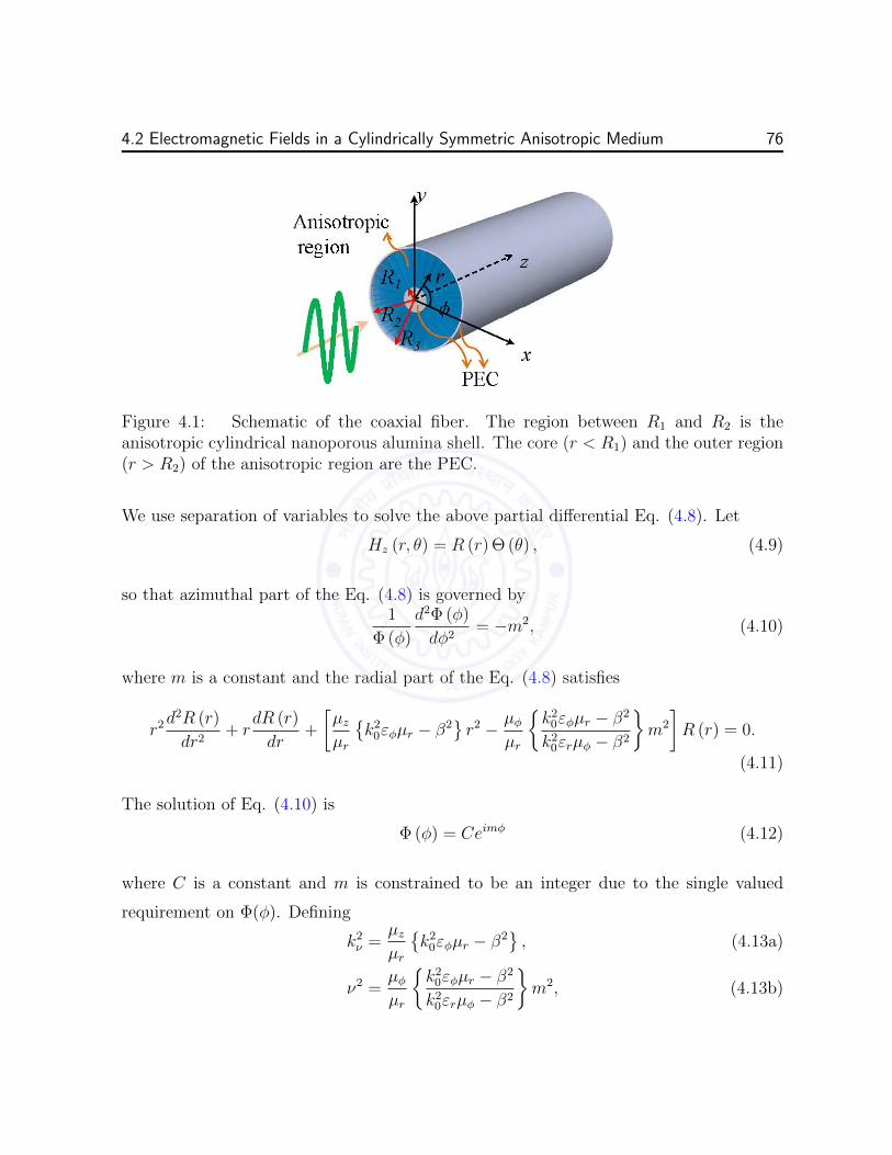
4.2 Electromagnetic Fields in a Cylindrically Symmetric Anisotropic Medium 76
Figure 4.1: Schematic of the coaxial fiber. The region between R1 and R2 is theanisotropic cylindrical nanoporous alumina shell. The core (r < R1) and the outer region(r > R2) of the anisotropic region are the PEC.
We use separation of variables to solve the above partial differential Eq. (4.8). Let
Hz (r, θ) = R (r) Θ (θ) , (4.9)
so that azimuthal part of the Eq. (4.8) is governed by1
Φ (φ)
d2Φ (φ)
dφ2= −m2, (4.10)
where m is a constant and the radial part of the Eq. (4.8) satisfies
r2d2R (r)
dr2+ r
dR (r)
dr+
[µzµr
k2
0εφµr − β2r2 − µφ
µr
k2
0εφµr − β2
k20εrµφ − β2
m2
]R (r) = 0.
(4.11)
The solution of Eq. (4.10) is
Φ (φ) = Ceimφ (4.12)
where C is a constant and m is constrained to be an integer due to the single valued
requirement on Φ(φ). Defining
k2ν =
µzµr
k2
0εφµr − β2, (4.13a)
ν2 =µφµr
k2
0εφµr − β2
k20εrµφ − β2
m2, (4.13b)

4.2 Electromagnetic Fields in a Cylindrically Symmetric Anisotropic Medium 77
then the Eq. (4.11) can be written as
r2d2R (r)
dr2+ r
dR (r)
dr+(k2νr
2 − ν2)R (r) = 0, (4.14)
which is the well known Bessel differential equation. Solving this equation we obtain the
radial dependence. A general form for the z component for the magnetic field is
Hz (r, φ, z, t) = A1Jν (kνr) + A2Yν (kνr) eimφei(βz−ωt). (4.15)
where Jν and Yν are the Bessel functions of first kind and second kind (Yν are also termed
Neumann functions). The coefficients A1 and A2 can be found by setting the tangential
components Eφ = 0 at PEC bundary R1 and R2 and we obtain the following condition
J′
ν (kνR1)Y′
ν (kνR2)− J ′
ν (kνR2)Y′
ν (kνR1) = 0, (4.16)
where prime (′) indicates the radial derivative. Solving this equation, we can obtain the
dispersion relations for TE modes.
The nature of the modes critically depends on the parameters ν and kν . It is well
known that when kν is imaginary, the modal solutions assume the form of the modified
Bessel functions. More importantly, in this case, the anisotropic nature of the waveguide
allows the order, ν, of the Bessel function to be fractional and even imaginary (ν2 <
0) [99, 100], which is not possible in isotropic systems. In a non-magnetic medium, for
example, a propagating (β is real) TE mode with real kν (implying that k20εφ > β2). If
k20εr < β2 < k2
0εφ, then ν2 < 0 and the order of the mode becomes imaginary. This is seen
to occur straightforwardly in a medium with εr < 0 and εφ > 0, whereas in a medium
with εr = εφ, this situation would not arise [88]. Note that the inequalities reverse if
we seek a TE mode with imaginary kν described by the modified Bessel functions. The
requirements for an imaginary order for the TM modes are actually slightly more involved
due to the various possibilities of the material parameters which is discussed in the next
subsection. By changing the sign of the dielectric permittivity components, there are
various kinds of solutions possible. All the possible solutions of the TE modes for various

4.2 Electromagnetic Fields in a Cylindrically Symmetric Anisotropic Medium 78
Table 4.1: Possible solutions for Hz in a non-magnetic (µr = µφ = µz = 1) homogeneousanisotropic circular coaxial waveguide.
Sr. εr εφ εz Conditions k2ν ν2 β Remarks
1 + + + k20εr > β2 + +
√k2
0εφ − k2ν
Solutions similar topositive index fibers,fractional order modes
k20εφ > β2
k20εr < β2 + −
√k2
0εφ − k2ν
Imaginary ordermodes
k20εφ > β2
k20εr > β2 − −
√k2
0εφ − k2ν
Imaginary ordermodes
k20εφ < β2
k20εr < β2 − +
√k2
0εφ − k2ν
Plasmonic surfacemodes
k20εφ < β2
2 + + − Hz same as 1
3 + − + k20εr > β2 − − i
√k2
0 |εφ|+ k2ν No propagation
−k20 |εφ| < β2
k20εr < β2 − + i
√k2
0 |εφ|+ k2ν No propagation
−k20εφ < β2
4 − + + −k20 |εr| < β2 + −
√k2
0εφ − k2ν
Imaginary ordermodes
k20εφ > β2
−k20 |εr| < β2 − +
√k2
0εφ − k2ν
Plasmonic surfacemodes
k20εφ < β2
5 + − − Hz same as 3
6 − + − Hz same as 4
7 − − + −k20 |εr| < β2 − + i
√k2
0 |εφ|+ k2ν No propagation
−k20 |εφ| < β2

4.2 Electromagnetic Fields in a Cylindrically Symmetric Anisotropic Medium 79
possibilities with anisotropic and non-magnetic materials are tabulated in Table 4.1.
Physical applications of Bessel functions with imaginary orders have been rarely
reported [99–101]. There are consequences to a fractional or imaginary order, ν. The
order of the Bessel function and the field distributions now depend on the propagation
constant β, unlike those for an integral order (m) mode in isotropic media. We notice in
Table 4.1 that the imaginary order modes (ν2 < 0) are even possible if the all permittivity
components are positive (Sr. 1 Table 4.1). There are some surface plasmonic modes as
presented by Table 4.1 Sr. no. 1, 4 and 6. In the plasmonic mode, the field decay along the
radial direction but can propagate along the axial direction. There is one very important
issue is that if the εφ < 0, then the propagation constant β becomes imaginary and there
is no propagation is possible for TE modes (Sr. 3,5,7 Table 4.1). The nature of the fields
of the modes described by the Bessel functions with imaginary orders will be discussed in
the later subsections of this chapter.
4.2.2 TM Modes in a Coaxial Anisotropic Fiber
Now we describe the TM modes in the coaxial anisotropic waveguide. The field compo-
nents for TM modes
Er 6= 0, Eφ 6= 0, Ez 6= 0, (4.17a)
Hr 6= 0, Hφ 6= 0, Hz = 0. (4.17b)
We again use the method of separation of variables and let
Ez (r, φ) = R (r) Φ (φ) . (4.18)
Following a similar approach as for the TE modes, for TM modes we can get the azimuthal
component of the Ez field as
Θ (φ) = Ceimφ, (4.19)

4.2 Electromagnetic Fields in a Cylindrically Symmetric Anisotropic Medium 80
where m is an integer and C is a constant. The radial part of Ez is the solution of the
differential equation
r2d2R (r)
dr2+ r
dR (r)
dr+(k2τr
2 − τ 2)R (r) = 0, (4.20)
in which
k2τ =
εzεr
k2
0εrµφ − β2, (4.21a)
τ 2 =εφεr
k2
0εrµφ − β2
k20εφµr − β2
m2. (4.21b)
If we see the expressions of the kν and ν in Eq. (4.13) of TE modes and the expressions
of the kτ and τ in Eq. (4.21) of TM modes are exactly complimentary to each other,
but with the permittivity replaced by the permeability components and vice versa. So to
avoid the confusion between the expressions of the TE and TM modes, we used different
symbols. The general form of the field component Ez of the TM mode is given by
Ez (r, φ, z, t) = B1Jτ (kτr) +B2Yτ (kτr) eimφei(βz−ωt). (4.22)
where kτ and τ is given by the Eq. (4.21). The coefficients B1 and B2 can be obtained by
setting the tangential components of the field, Ez = 0 for the field at the PEC boundaries,
resulting in
Jν (krR1)Yν (krR2)− Jν (krR2)Yν (krR1) = 0. (4.23)
This the dispersion relation of the TM modes of the coaxial waveguides. After taking
the various combinations of the sign of permittivity components, there are various types
of solutions possible. All these solutions for a non-magnetic anisotropic circular coaxial
fiber are listed in Table 4.2. Due to the involvement of εz in Eq. (4.21a), there some more
solutions that are not possible in the case of TE mode of non-magnetic and anisotropic
circular coaxial fiber as we have seen in the Table 4.1 of the previous subsection . In the
TM mode case, if the εz < 0 then in some cases when there are modes with essentially no
cutoff frequency (Sr. 2,5 Table 4.2). Here there is only one case εr < 0, εz < 0 for which
there is no propagation (Sr. 6 Table 4.2).

4.2 Electromagnetic Fields in a Cylindrically Symmetric Anisotropic Medium 81
Table 4.2: Possible solutions for Ez in a non-magnetic (µr = µφ = µz = 1) homogeneousanisotropic circular coaxial waveguide.
Sr. εr εφ εz Conditions k2τ τ 2 β Remarks
1 + + + k20εr > β2 + +
√k2
0εr − εrεzk2τ
Solutions similar topositive index fibers,fractional order modes
k20εφ > β2
k20ερ > β2 + −
√k2
0εr − εrεzk2τ
Imaginary ordermodes
k20εφ < β2
k20εr < β2 − −
√k2
0εr − εrεzk2τ
Imaginary ordermodes
k20εφ > β2
k20εr < β2 − +
√k2
0εr − εrεzk2τ
Plasmonic surfacemodes
k20εφ < β2
2 + + − k20εr > β2 − +
√k2
0εr + εr|εz |k
2τ No cutoff
k20εφ > β2
k20εr > β2 − −
√k2
0εr + εr|εz |k
2τ No cutoff
k20εφ < β2
k20εr < β2 + −
√k2
0εr + εr|εz |k
2τ No cutoff
k20εφ > β2
k20εr < β2 + +
√k2
0εr + εr|εz |k
2τ No cutoff
k20εφ < β2
3 + − + k20εr > β2 + +
√k2
0εr − εrεzk2τ
Solutions similar topositive index fibers,fractional order modes
−k20 |εφ| < β2
k20εr < β2 − −
√k2
0εr − εrεzk2τ
Imaginary ordermodes
−k20 |εφ| < β2

4.2 Electromagnetic Fields in a Cylindrically Symmetric Anisotropic Medium 82
Sr. εr εφ εz Conditions k2τ τ 2 β Remarks
4 − + + −k20 |εr| < β2 + +
√−k2
0 |εr|+|εr|εzk2τ
Fractional ordermodes
k20εφ > β2
−k20 |εr| < β2 + −
√−k2
0 |εr|+|εr|εzk2τ
Imaginary ordermodes
k20εφ < β2
5 + − − k20εr > β2 − +
√k2
0εr + εr|εz |k
2τ No cutoff
−k20 |εφ| < β2
k20εr < β2 + −
√k2
0εr + εr|εz |k
2τ No cutoff
−k20 |εφ| < β2
6 − + − −k20 |εr| < β2 − + i
√k2
0 |εr|+|εr||εz |k
2τ No propagation
k20εφ > β2
−k20 |εr| < β2 − − i
√k2
0 |εr|+|εr||εz |k
2τ No propagation
k20εφ < β2
7 − − + −k20 |εr| < β2 + +
√−k2
0 |εr| −|εr|εzk2τ
Fractional ordermodes
−k20 |εφ| < β2

4.3 Modal Fields and Dispersions in a homogeneously filled anisotropic coaxial waveguide 83
4.3 Modal Fields and Dispersions in a homogeneously
filled anisotropic coaxial waveguide
In Chapter 3, we homogenized a cylindrically symmetric microwire of nanoporous alu-
mina and found that it has uniaxial anisotropy, i.e., εr 6= εφ = εz. Due to the varying fill
fraction with the radial distance, the alumina microtube is actually an inhomogeneously
filled anisotropic waveguide. However, to understand the nature of the modes in cylindri-
cally anisotropic medium, it would be good to separate out the effects of anisotropy and
inhomogeneity. Hence, in this section, we analyze the modes of a homogeneously filled
anisotropic waveguide. As an approximation, let us assume that the nanoporus alumina
fiber is homogeneously filled and it has uniaxial anisotropy. Additionally PEC boundary
conditions are applied symmetrically at r = R1 and r = R2 thereby reducing it to a
coaxial waveguide.
In the previous section, we discussed the general solutions of TE and TM modes
of a homogeneously filled anisotropic (εr 6= εφ 6= εz) coaxial waveguide. If in the Tables
4.1 and 4.2, we use the anisotropy as εr 6= εφ = εz then the number of possibilities
are reduced. From these two tables we have noticed that the TM modes present more
interesting cases with than the TE modes with dielectric anisotropy. For example, there
are modes with no cut-off frequencies in some cases. Hence we discuss the TM modes
here. The numerical analysis of the TE modes can be done in a similar manner. As we
have seen, the nanopores of cylindrical nanoporous alumina microtube can be filled with
suitable materials like polymers, liquids, metals etc. which can give different signs to
the different permittivity components. Here we considered two cases to demonstrate the
nanoporous alumina coaxial fiber. First the nanopores filled with air and the second the
nanopores filled with silver metal.
In this chapter we have used mode index notation TMm,n to avoid the confusion for
higher index modes, where m is the azimuthal integral order of the mode which appears in
the solution of the angular part of Eq. (4.12) or (4.19), and n is the sequence of number of

4.3 Modal Fields and Dispersions in a homogeneously filled anisotropic coaxial waveguide 84
roots of dispersion relation for a fixed azimuthal order m. Since in the anisotropic coaxial
waveguides there can exist the integral, fractional and imaginary order modes, therefore,
in the next subsection we shall briefly introduce about the Bessel functions of various
kinds of orders which will help to understand the nature of the modes of the anisotropic
fiber.
4.3.1 Bessel Functions of Integral, Fractional and Imaginary Or-ders
The Bessel functions are the solutions of the Bessel differential equation [102]
x2 d2y
dx2+ x
dy
dx+ (x2 − α2)y = 0, (4.24)
where constant α is called the order of the Bessel functions. The above equation have
two solutions which are called Bessel functions of first kind (Jα) and Bessel functions of
second kind or Neumann function (Yα). For the purely imaginary argument the solutions
of the Eq. (4.24) are called Modified Bessel function of first kind (Iα) and Modified Bessel
function of second kind (Kα). The Bessel functions order, α, can be integral, fractional,
imaginary or complex numbers which will reflect on the properties of the Bessel functions.
Some plots of Bessel functions of different kind of orders are shown in Fig. 4.2 [103].
We see that the integral order Bessel functions either oscillate or decay as shown in
Fig. 4.2(a) and 4.2(b). In the integral order case the minimum variation of α is 1, while
this variation in the fractional order case can be extremely small. The fractional order
Bessel functions also oscillate or decay but their variation with the order α become slow
or fast as the functions orders slow or fast than the integral order Bessel functions. For
example in the Fig. 4.2(c) the functions orders are 1/2 and 1/3 then the variation in the
function is small. If the function order would become 1/2.1 or 17/2 then the function
would change very slow or fast compared to the function of order 1/2. Similarly this
also happens for the modified Bessel functions too, but only thing is that they always
decay with increasing x. The behavior of the imaginary order Bessel functions are very

4.3 Modal Fields and Dispersions in a homogeneously filled anisotropic coaxial waveguide 85
(a) (b)
(c) (d)
(e) (f)
Figure 4.2: Plots of the Bessel functions Jα and Yα (left panel), and plots of the ModifiedBessel functions Iα and Kα (right panel). Plots of (a) and (b) for integral order, (c) and(d) for fractional order, and (e) and (f) for imaginary order (Olver et al., NIST Handbookof Mathematical Functions,2010).

4.3 Modal Fields and Dispersions in a homogeneously filled anisotropic coaxial waveguide 86
different than the integral and fractional order Bessel functions. They always oscillate
whether they are ordinary Bessel functions (Fig. 4.2(e)) or Modified Bessel functions(Fig.
4.2(f)). As the argument, x, decrease, the functions oscillations increase. The functions
amplitudes and oscillations increase tremendously with their order as argument tends to
zero. In fact, these functions do not have a well defined limit as x→ 0, and are reminiscent
functions like sin(1/x) that have an essential singularity at x = 0. More details of the
Bessel functions can be found in Ref. [103]. In the next subsection, we shall use these
Bessel functions to explain the mode properties of the homogeneously filled anisotropic
coaxial waveguides.
4.3.2 Modal Fields in homogeneous Anisotropic Waveguides
At cut-off, every type of mode has an integral order, the order τ or ν of the Bessel function
changes with β or the frequency, ω, for a given m. One of the consequences is that the
modes become comparatively more confined near the center with increasing β or ω. This
confinement is more drastic than in ordinary dielectric fibers as the effects of β or ω
are manifested within the Bessel functions order (τ or ν) rather than only the argument
(kr). Figure 4.3 shows this behavior for the TM1,1 and TM 2,2 modes. In contrast to a
waveguide filled with an isotropic medium where the argument of the Bessel function (kr)
changes with β, here, the order ν of the Bessel function itself evolves with β. In Fig. 4.3,
this is strictly true that at β = 0 represents the onset of a stop band and a condition
where the modes may be described purely as TE or TM, hence, it is not unreasonable to
show them as we have also shown alongside the field distributions for β 6= 0. We highlight
that the field profile for the first two sub-figures varies subtly for the non-zero beta value
shown in the remaining figures, as a result of the mode order becoming fractional from a
integral one.
For air inclusions and at 0.23 fill fraction, the field component (Ez) for the TM
modes is plotted in Fig. 4.4. In this figure, the first row is for an isotropic alumina

4.3 Modal Fields and Dispersions in a homogeneously filled anisotropic coaxial waveguide 87
Figure 4.3: The behavior of low-order modes (TM1,1 and TM2,2) in an anisotropicnanoporous alumina coaxial fiber for dimensions R1 = 0.5 µm and R2 = 12.5 µm. Col. 1:Eigen modes at β = 0, τ = m integral order, Col. 2: modes at εr = 2.467, εφ = εz = 2.638,and β 6= 0, τ 6= m fractional order, Col. 3: modes at εr = 2.638, εφ = εz = 2.467, andβ 6= 0, τ 6= m imaginary order. Dielectric constants are at wavelength 633 nm.
fiber with positive εr = εφ = εz = 3.118 at wavelength λ = 632.8 nm for reference.
In the case of an air filled nanoporous fiber with εr = 2.467, εφ = εz = 2.638, there
are fractional order modes possible at wavelength λ = 632.8 nm as shown in Fig. 4.4.
We see that the confinement of the electric field is higher than the isotropic fiber. It
is more visible for the higher order modes. Imaginary order modes are also possible for
εr = 2.638, εφ = εz = 2.467, and λ = 632.8 as shown in Fig. 4.4. Here the confinement of
light within the fiber is very high and the light is highly concentrated towards the center
of the fiber. For the imaginary order modes, as the index m increases, the fields spread
all over the volume while concentrating towards the center. By contrast, in the isotropic
fiber with positive ε, the fields move away from the center of the fiber for large azimuthal
index m. These modes that are localized to the edge of the fiber are conventionally termed
“whispering gallery modes”.
Metals have complex permittivity with negative real parts below their plasma fre-

4.3 Modal Fields and Dispersions in a homogeneously filled anisotropic coaxial waveguide 88
Figure 4.4: The computed electric fields (Ez) of modes in cylindrical nanoporous aluminawhen nanopores have air inclusion for R1 = 0.5 µm, R2 = 12.5 µm for m = 1, 2, 5, 20, 40.Top row shows the Bessel modes in an isotropic alumina fiber with real integral orders forεr = εφ = εz = 3.118. The middle row shows Bessel modes in an anisotropic nanoporousalumina fiber with fractional order and positive dielectric permittivity components forεr = 2.467 and εφ = εz = 2.638. The bottom row shows the fields for Bessel modes ofanisotropic nanoporous alumina fiber with imaginary orders and εr = 2.638 and εφ =εz = 2.467. Relative permittivity components are at wavelength 632.8 nm.

4.3 Modal Fields and Dispersions in a homogeneously filled anisotropic coaxial waveguide 89
Figure 4.5: The computed electric fields (Ez) of modes in cylindrical nanoporous alu-mina when nanopores have silver metal inclusion for R1 = 0.5 µm, R2 = 12.5 µm form = 1, 2, 5, 20, 40. The fields for Bessel modes of anisotropic nanoporous alumina fiberwith complex orders and εr = −1.288 + i0.053 and εφ = εz = 6.244 + i0.027. Relativepermittivity components are at wavelength 632.8 nm.
quencies which lie in UV range for most of the metals. Filling the nanopores of the
cylindrical nanoporous alumina with silver metal, the effective permittvity components
of the cylindrical nanoporous alumina show the hyperbolic dispersion in some frequency
range. Field plots for TM modes for the case of silver inclusion in nanoporous alumina
with εr = −1.288+i0.053, εφ = εz = 6.244+i0.027 at wavelength λ = 632.8 nm have been
shown in Fig. 4.5. We see that the modes are confined like the imaginary order modes
of the air inclusion case. But in the silver inclusion case, complex order modes are also
possible because of the complex permittivity of the metal. Here also the fields are spread
over the volume while concentrating towards the fiber axis. If we vary the real part of the
dielectric permittivity and keeping imaginary part of the dielectric permittivity constant
then it will change the cutoff frequency of the modes and field confinement, but no change
in the losses will occur. The change of the cutoff and confinement also depend on the
levels of the anisotropy. On the other hand, if we keep real part of the dielectric permit-
tivity constant and vary the imaginary part, then it will increase the losses drastically and
slight change on the cutoff and field distribution. For smaller imaginary part of dielectric
permittivity losses will be lower and for larger imaginary part of dielectric permittivity
the losses will be higher. In all the applications, there is a need to keep imaginary part
of dielectric permittivity small as much as it can be.
The modes with imaginary orders are very interesting in that the higher-order (large
4.3 Modal Fields and Dispersions in a homogeneously filled anisotropic coaxial waveguide 90
m) modes are localized near the central region of the waveguide (see Fig. 4.4). In contrast,
the large m whispering gallery modes are concentrated at the edges of a waveguide filled
with an isotropic positive material (Fig. 4.2). Further, these Bessel functions with imagi-
nary orders undergo large oscillations near the center and need not converge at r = 0 [99],
a reflection of the geometric singularity at the axis, which cannot be attained in a physical
system. The PEC boundary condition applied at r = R1, however, prevents any issues
with the mathematical singularities of the function at the origin (r = 0). The number of
oscillations of the wave-field near r = 0 increases with the order τ (or ν) of the mode.
Even for modes with real fractional orders that result for anisotropic fibers, there is a
comparatively larger confinement of the higher-order m modes (Fig. 4.4).
The origin of this spreading out of the fields of the modes with large m well into the
interior of the waveguide lies in the dispersion of the wave in a hyperbolic medium with
cylindrical symmetry. Consider at very small length scales, when a wave propagating in
the (r, φ) plane would essential look like a plane wave, so that the local wave-vector can
be considered to be along the ray. If (kr, kφ) be locally the wave-vector, the phase shift
for an infinitesimal displacement (δr, rδφ) would be exp[i(krδr + kφrδφ)]. Demanding a
single valued function constrains that kφ = m/r, where m is an integer. Under these
circumstances (in analogy to a wave in an anisotropic medium in flat rectangular space),
locally we havek2r
εφ+
m2
r2εr=ω2
c2. (4.25)
In a normal positive medium with εr > 0 and εφ > 0, as the wave moves towards
the origin, r → 0 and kφ → ∞, and kr becomes imaginary. Thus, the wave decays
exponentially towards the origin for the large m whispering gallery modes and avoids the
region near the origin. On the contrary, in an hyperbolic medium with εr · εφ < 0, kr
remains real and large for kφ → ∞ (large m), and the wave can effectively propagate
in the region near the origin with the only difference that the fields oscillate more and
more rapidly along r closer to the origin. This is due to the fact that propagation of

4.3 Modal Fields and Dispersions in a homogeneously filled anisotropic coaxial waveguide 91
higher-order modes that can be supported in media with hyperbolic dispersion as seen
earlier in the case of the hyperlens [104]. In that work, the higher-order modes carrying
spatially sub-wavelength (rapidly varying) image features could be propagated across the
radial direction and imaged out into far-field radiating modes [12]. For example, in Eq.
(4.25), if εr < 0 and εz > 0, then kr increases without bound along with β. Thus, very
large oscillatory field variations in the radial direction can be supported close the center
of the fiber and the field can occupy large modal volumes.
4.3.3 Modal Dispersions in Homogeneous Anisotropic Waveg-uide
We proceeded then to calculate the dependence of the propagation constant β on the
frequency (the dispersion) for the anisotropic waveguide. The Fig. 4.6 shows the disper-
sions in an nanoporous alumina fiber with air and silver inclusions at fill fraction of 0.23
and 0.08 respectively. In the 1-35 THz frequency range, alumina has a number phonon
resonances. So we used experimental data for the dielectric permittivities of the alumina
host [105] and the silver inclusion [7, 106]. For comparison the modal dispersion of the
isotropic alumina fiber is also shown. The cutoff frequencies of modes of isotropic alumina
fiber and anisotropic nanoporous alumina fiber for air inclusion are calculated in the 1-35
THz range and tabulated in the Tables 4.3 and 4.4 respectively.
As shown in Fig. 4.6(a), the alumina has phononic resonances at 13 THz and 17 THz,
which cause strong dispersion in the effective permittivity of the nanoporous alumina.
Both fibers, isotropic as well as anisotropic, show forward wave propagation from 5.5-
11.5 THz. In this range losses (Im(β) << Re(β)) are very small and fibers are suitable
for practical applications. Because of phononic resonance of alumina, from 11.5-22 THz
range there are several narrow bands of backward and forward wave propagation. The
backward propagating waves usually have extreme losses. In the 22-25.7 THz frequency
range, there is negative phase velocity with high loss in the nanoporous alumina fiber for

4.3 Modal Fields and Dispersions in a homogeneously filled anisotropic coaxial waveguide 92
(a) (b)
Figure 4.6: The computed TM1,1 dispersive dispersion of modes in cylindrical nanoporousalumina when nanopores have (a) air inclusion with fill fraction 0.23 and (b) silver inclu-sion with fill fraction 0.08. R1 = 0.5 µm, R2 = 12.5 µm. The air permittivity was 1, thepermittivity of alumina taken from Ref. Rajab et al. 2008 and for silver from Ref. Ordalet al. 1983.
Table 4.3: The dispersive cutoff frequencies (in THz) of TM modes of a non-magnetichomogeneous isotropic alumina coaxial fiber. Cutoff frequencies are calculated in the 1-35THz frequency range for various modes.
Mode fc1(THz) fc2(THz) fc3(THz)TM0,1 3.6371 - i 0.0063 14.9586 - i 0.1575 27.5003 - i 0.3531TM0,2 7.0699 - i 0.0265 15.0282 - i 0.1524 29.2919 - i 0.2667TM1,1 4.5847 - i 0.0102 14.9684 - i 0.1566 27.8242 - i 0.3339TM1,2 7.6983 - i 0.0323 15.0601 - i 0.1509 29.8815 - i 0.2461
air inclusion only which is not possible in isotropic fibers. This is a very unique feature of
the nanoporous alumina. Beyond 25.7 THz the nanoporous alumina fibers again become
useful for applications.
For the case of silver inclusion in the nanoporous alumina, the high negative permit-
tivity of silver always dominates over the permittivity of alumina host and creates extreme
anisotropy. Since the metals are very lossy media. Therefore, including the metals into
the structured system such as nanoporous alumina increases the loss in the anisotropic
system. Figure 4.6(b) shows the dispersion and Table 4.5 shows the cutoff frequencies of

4.3 Modal Fields and Dispersions in a homogeneously filled anisotropic coaxial waveguide 93
Table 4.4: The dispersive cutoff frequencies (in THz) of TM modes of a non-magnetichomogeneous nanoporous alumina coaxial fiber for air inclusion in the nanopores. Cutofffrequencies are in the 1-35 THz frequency range.
Mode fc1(THz) fc2(THz) fc3(THz) fc4(THz)TM0,1 4.3450 - i 0.0085 14.9262 - i 0.1599 24.1951 - i 0.6636 27.3489 - i 0.3619TM0,2 8.1955 - i 0.0359 15.0640 - i 0.1501 24.8165 - i 0.5454 29.0552 - i 0.2651TM1,1 5.4478 - i 0.0138 14.9681 - i 0.1565 24.3554 - i 0.6256 27.6089 - i 0.3441TM1,2 8.8376 - i 0.0436 15.1223 - i 0.1487 24.9237 - i 0.5322 29.7192 - i 0.2384
the waveguide modes with silver nanowire inclusions in the nanopores of the cylindrical
nanoporous alumina. The Fig. 4.6(b) shows that there is extreme loss (Im(β) >> Re(β))
over almost the entire range. But in a very wide frequency range, from 6.6-25.5 THz,
there is backward wave propagation effectively. In a narrow band around 14.5 THz and a
wide band 26-28.3 THz, there is negative phase velocity. The nanoporous alumina with
silver inclusion from 27-28 THz might be potentially useful for applications because of
lower losses.
The losses due to the metal inclusion vary over the electromagnetic spectrum. These
losses are very less in the visible range. The solutions for modes for homogenized fibers
corresponding to silver-filled nanoporous alumina, the ratio of the imaginary and real parts
of β at 632.8 nm wavelength was on the order of 10−3 for TM1,1 modes (f = 0.08) with
complex order. Thus, while the fibers discussed here are clearly not meant for traditional
transmission applications, they have immense potential for several other purposes such as
coupling the near-field into a waveguide or waveguide couplers and shifters. The complex
order modes always will be lossy. While absorption can not be removed totally, but it can
be lowered down with very dilute metallic inclusions. For very dilute metallic inclusions
with very low fill fraction, we may not obtain hyperbolic dispersions. So we have to
optimize the parameters of the dielectric permittivity to obtain complex order modes as
per need.
For non-metallic inclusions, we can get the situation where Re(β) >> Im(β), as

4.4 Guided Modes in Homogeneously Filled Anisotropic Hollow Fiber 94
Table 4.5: The dispersive cutoff frequencies (in THz) of TM modes of a non-magnetichomogeneous nanoporous alumina coaxial fiber for silver metal inclusion in the nanopores.Cutoff frequencies of fibers are in the 1-1500 THz frequency range.
Mode fc1(THz) fc2(THz) fc3(THz)TM0,1 3.3632 - i 0.0054 14.9565 - i 0.1577 27.4242 - i 0.3580TM0,2 6.6161 - i 0.0228 15.0111 - i 0.1534 28.9349 - i 0.2807TM1,1 4.2489 - i 0.0087 14.9645 - i 0.1570 27.6980 - i 0.3412TM1,2 7.2308 - i 0.0280 15.0353 - i 0.1520 29.4314 - i 0.2616
for example can be seen in Fig. 4.6(a) in the case of air inclusion. In this situation the
losses will be almost zero and such arrangement can be used for practical purpose. As
we see in the previous paragraph in the case of metallic inclusions, the losses are so high
that in this case the waveguide may not be practically suitable for applications, although
this arrangement has hyperbolic dispersion. But, if we are able to fill the nanopores with
such electrically conducting materials that have almost zero imaginary part of dielectric
permittivity (very low loss), then we can get Re(β) >> Im(β) and hyperbolic behavior
simultaneously.
4.4 Guided Modes in Homogeneously Filled Anisotropic
Hollow Fiber
It is also important to realize that the general nature of these modal solutions are not
limited by the application of PEC boundaries. The only restriction would be for the
nanoporous alumina regions to have a larger dielectric permittivity than the surrounding
medium. Having dielectric boundaries, for example by having a hollow core and no
aluminum coating on the outer surface, causes the waveguide to be inhomogeneous and
support hybrid (the so-called HE and EH) modes. Fibers with hollow cores are important
for various issues of confinement of light as in hollow core photonic crystal fibers.
Now we consider a general case in which the PEC condition in the core (r < R1) and

4.4 Guided Modes in Homogeneously Filled Anisotropic Hollow Fiber 95
outside region (r > R2) of the homogeneously filled waveguide have been relaxed (4.1).
Assuming that in core and the outside region have same non-magnetic and isotropic
material with dielectric permittivity ε1, then the nature of the field be same in core and
outer region. For the guided modes the longitudinal field components in region 1, 2 and
3 can be expressed as
E1z = C1Iτ1(γτ1r)eimφei(βz−ωt), (4.26a)
H1z = C2Iν1(γν1r)eimφei(βz−ωt), (4.26b)
E2z = (C3Jτ2(γτ2r) + C4Yτ2(γτ2r))eimφei(βz−ωt), (4.26c)
H2z = (C5Jν2(γν2r) + C6Yν2(γν2r))eimφei(βz−ωt), (4.26d)
E3z = (C7Kτ3(γτ3r))eimφei(βz−ωt), (4.26e)
H3z = (C8Kν3(γν3r))eimφei(βz−ωt), (4.26f)
where τ ’s and ν’s are given by Eqs. (4.21b) and (4.13b) respectively, and γτ ’s and γν ’s
by the following expressions:
γτi =εziεri
√ω2εriµφi − β2, (4.27a)
γνi =µziµri
√ω2εφiµri − β2. (4.27b)
Substituting Eqs. (4.26) in Eqs. (4.6) the transverse components can be obtained.
Equating the parallel components of the fields at boundary R1 and R2 we get eight
homogeneous equations in eight unknowns. For existence of the non-trivial solutions,
the determinant of the coefficient matrix must be zero. This determinant is solved for
β to obtain the dispersion relations. Considering that in the region 2 the solutions are
oscillatory, then for εr > 0, εφ > 0 and εz > 0, the guided mode conditions will be
ε1 < β2/k20 < εr, and ε1 < β2/k2
0 < εφ. (4.28)
For the guided modes, when εr > εφ, there is one condition called the normalized propa-
gation constant defined as
V = k0R2
√εφ − ε1. (4.29)

4.4 Guided Modes in Homogeneously Filled Anisotropic Hollow Fiber 96
(a) (b)
Figure 4.7: The modal dispersions of the homogeneously filled nanoporous aluminahollow waveguides embedded in air and when the nanopoers are filled with (a) air for fillfraction 0.23 and (b) silver metal for fill fraction 0.08. The permittivity of alumina takenfrom Ref. Rajab et al. 2008 and for silver from Ref. Ordal et al. 1983.
Similarly if εr < 0, εφ > 0 and εz > 0, then the condition for a guided mode will be
− |εr| < β2/k20, and ε1 < β2/k2
0 < εφ, (4.30)
and the normalized propagation constant will be same as when all the permittivity com-
ponents are positive. By choosing the different signs for the dielectric permittivity com-
ponents, there are only few cases that are listed in Table 4.6 where the guided modes are
possible. Let a = 5µm and b = 15µm, then for the nanoporous alumina fiber with air in-
clusion embedded in air, at visible frequency He-Ne laser wavelength, the V is 180.34. But
for an isotropic fiber where the where the core and clad have indexes 1.4457 and 1.4378
respectively, V is 11.99. This demonstrates that more number of guided modes will exist
in the nanoporous alumina fiber for these conditions and this number will change over
changing the frequency. The number of guided modes will reduce at smaller frequencies.
The Fig. 4.7 shows the modal dispersions of the homogenepusly filled nanoporous alu-
mina hollow waveguide embedded in air with air and silver metal inclusions. The modal
dispersion of isotropic alumina fiber is also shown for comparison. We see that the change
of the normalized β is very small compared to the case of an isotropic fiber. This hap-

4.4 Guided Modes in Homogeneously Filled Anisotropic Hollow Fiber 97
Table 4.6: Guided mode conditions of a non-magnetic homogeneous anisotropic hollowcircular waveguide. Where dielectric constant of core and outer region are ε1 = ε3 = εi.The index i for isotropic material.
Sr. εr εφ εz k2ν k2
τ Conditions
1 + + + k20εφ − β2 εz
εr(k2
0εr − β2) εi < β2/k20 < εr
εi < β2/k20 < εφ
2 + + − k20εφ − β2 −|εz |
εr(k2
0εr − β2) εr < β2/k20
εi < β2/k20 < εφ
3 + − + −k20 |εφ| − β2 εz
εr(k2
0εr − β2) No guided mode
4 − + + k20εφ − β2 εz
|εr| (k20 |εr|+ β2) − |εr| < β2/k2
0
εi < β2/k20 < εφ
5 + − − −k20 |εφ| − β2 −|εz |
εr(k2
0εr − β2) No guided mode
6 − + − k20εφ − β2 |εz |
|εr| (−k20 |εr| − β2) No guided mode
7 − − + −k20 |εφ| − β2 εz
|εr| (k20 |εr| − β2) No guided mode

4.5 Conclusions 98
(a) (b) (c) (d)
Figure 4.8: The normalized mode plots of the homogeneously filled nanoporous aluminawaveguide, when the nanopores are filled with air and silver, at wavelength 632.8 nm. (a)and (b) are modes for air inclusion, εr = 2.638, εφ = 2.467. (c) and (d) are modes forsilver inclusion, εr = −1.288+ i0.053, εφ = 6.244+ i0.027. Here the core radius R1 = 5µmand nanoporous alumina shell radius R2 = 15µm.
pens because of the effective orders ν and τ of the Bessel functions for magnetic field and
electric field become fractional and changes very slowly with increasing with azimuthal
number m. Some plots of the modes in homogeneously filled anisotropic nanoporous alu-
mina waveguide, when nanopores filled with air and silver nanowires at fill fraction 0.23,
at wavelength 632.8 nm are shown in Fig. 4.8. For this example, the core (r < R1 = 5µm)
and outer region (r > R2 = 15µm) of the homogeneous hollow anisotropic waveguide are
assumed to be air. When the nanopores of anisotropic region are filled with air, then
this is corresponds to Sr no. 1 of Table 4.6. Similarly, when the nanopores of anisotropic
region are filled with silver nanowires, then this case is correspond to Sr. no. 4 of the
Table 4.6. We see that the whole field is confined into the anisotropic region and in the
core and outer region the field is almost zero.
4.5 Conclusions
We have presented a sample of the astonishing range of possibilities that arise with
anisotropic metamaterial optical fibers. In this chapter, we have given a general mathe-
matical description of nature of wave propagation in the anisotropic metamaterial fibers

4.5 Conclusions 99
and numerically analyzed some practically possible examples of nanoporous alumina meta-
material fibers. These anisotropic metamaterial fibers support exotic modes described by
Bessel and Neumann functions of fractional, imaginary and complex order, a rare physi-
cal application of these mathematical objects. A detailed analysis of the modes that are
possible for the coaxial geometry under different kinds of anisotropies is presented. The
conditions under which the modes are described by Bessel functions with imaginary orders
or complex orders are investigated. These are shown to arise from hyperbolic dispersion
in the medium. Many of the properties presented here are generic to circular waveguides
with anisotropic metamaterial fillings and have wide ranging applications across the elec-
tromagnetic spectrum from the radio frequencies to optical frequencies. The nanoporous
alumina microtubes with or without a central hollow core are presented as a physical
manifestation of such an anisotropic metamaterial optical fiber. Here the guidance of the
modes is entirely due to refractive effects and the condition for guided modes are ana-
lyzed. These metamaterial fibers with metallic inclusions exhibit electromagnetic losses
by absorption and can not be used for communication purposes. But unique range of
properties offered by them can be best utilized for sensing, coupling and other non-linear
applications.


Chapter 5
Inhomogeneous, AnisotropicMetamaterial Optical Fiber
5.1 Introduction
The optical fibers or waveguides that have been homogeneously filled with an anisotropic
dielectric material had been studied and used in various applications from several decades.
In the step index fiber, the core and the clad are homogeneous. The inhomogeneous
optical fibers have been less popular compared to homogeneous optical fibers [97,107,108].
This was presumably because of the difficulty in fabrication of the desired inhomogenious
distribution of materials and the difficulty in predicting the properties as well. A quadratic
inhomogeneous in permittivity optical fibers had been reported, which can be solved
approximately in closed form [108,109]. Fibers with parabolic profile in the radial direction
for the refractive index have been popular as they strongly localize the electromagnetic
wave into the fiber. The FEM numerical technique is commonly used to solve such type of
inhomogeneous problems [110–112]. An inhomogeneous fiber made of anisotropic liquid
crystals with homogeneous material clad has also been reported [113]. In this liquid
crystal fiber an angular inhomogeneity was present while the earlier fibers only have a
radial inhomogeneity in the refractive index. After the invention of the photonic crystal,
101

5.2 Inhomogeneous Nature of Cylindrical Nanoporous Alumina 102
a few inhomogeneous photonic crystal fibers have been reported to support spatial soliton
formation and to change the spectral properties of the fibers [114,115].
In the previous Chapter 4, we presented the modal analysis of a homogeneously
filled nanoporous alumina metamaterial coaxial fiber. In fact, the cylindrical nanoporous
alumina is actually an inhomogeneous medium because of the varying nature of the size of
the nanopores along the radial direction. In the previous chapter, we considered that the
nanoporous alumina is homogeneous for simplicity and to understand the effects of the
anisotropy only. Otherwise, we could not have distinguished the effects of inhomogeneity
and anisotropy. In the present chapter, we shall discuss about the propagation of light and
analyze the modes in inhomogeneous and anisotropic nanoporous alumina coaxial/hollow
fiber. We shall see that in the inhomogeneous fiber, the electric and magnetic fields can
not be decoupled and the modal solutions are not always amenable to analytic solutions.
To study the waveguide properties of the inhomogeneous and anisotropic nanoporous
alumina fiber, we carry out the analysis using the COMSOL Multiphysics simulations.
5.2 Inhomogeneous Nature of Cylindrical Nanoporous
Alumina
We have seen in the previous Chapters 2 and 3, that the diameter of the nanopores and
the azimuthal interpore distance in the cylindrical nanopores decrease towards the center
of the fiber. Equation (3.9) shows that the nanopores fill fraction is a linear function of
fiber radius which makes the cylindrical nanoporous alumina an inhomogeneous system.
For a fixed radius of an aluminium microwire, the size of the nanopores and the interpore
distance at the outer surface of the anodized wire can be changed by electrolyte, anodiza-
tion voltage or current and solution temperature. Keeping the interpore distance fixed,
the nanopores size even can be increased by pore widening. As we have seen in Chapter
2, at 40 V anodization of aluminium microwire in an iced cold 0.3 M oxalic acid solution
gives average 30 nm nanopore diameter and average 100 nm interpore distance. Later

5.2 Inhomogeneous Nature of Cylindrical Nanoporous Alumina 103
Figure 5.1: Plot of the fill fraction of nanopores of the cylindrical nanoporous aluminawith microtube radius r and the diameter of the nanopores 2Q at the outer surface atR2. Here interpore distance D = 100 nm, R1 = 0.5 µm, R2 = 12.5 µm.
on the nanopore diameters can be increased up to below the interpore distance by pore
widening in dilute phosphoric acid. For a fixed interpore distance of 100 nm, the Fig. 5.1
show the plot of the nanopores fill fraction of the cylindrical nanoporous alumina with
respect to the radius of the fiber and the nanopore diameter (2Q) at the outer surface.
We see that for smaller nanopores diameter the variation of the fill fraction along the fiber
radius is smaller and this variation increases for the bigger nanopore diameters, that is,
the inhomogeneity and the anisotropy increase with the nanopores diameter.
The effective permittivity tensor components of the cylindrical nanoporous alumina
are obtained in Eqs. (3.17), (3.18) and (3.19), by using the transformation optics technique
and the Maxwell-Garnett homogenization theory. They have been plotted in Fig. 5.2 with
respect to the radius of the fiber and frequency for the case of air inclusions and 50 nm
nanopores diameter and 100 nm interpore distance. For lower frequency ranges, there is
a resonance in the effective permittivity components εr and εφ = εz as shown in Figs.
5.2(a) and 5.2(b). But at visible range of frequencies, the εr and εφ are almost varying
linear with the fiber radius at fixed frequency as shown in Figs. 5.2(c) and 5.2(d). Near
the resonance, the anisotropy in the permittivity components is high and beyond the
resonance the anisotropy is very small.

5.2 Inhomogeneous Nature of Cylindrical Nanoporous Alumina 104
(a) (b)
(c) (d)
Figure 5.2: Plots of the effective permittivity components εr and εφ with frequency andradius of the fiber for 2Q = 50 nm, D = 100 nm. (a) and (b) for 1 THz to 50 THzfrequency range, (c) and (d) for the visible range.

5.3 Electromagnetic Fields in Inhomogeneous andAnisotropic Cylindrical Media 105
5.3 Electromagnetic Fields in Inhomogeneous and
Anisotropic Cylindrical Media
We have given the detailed mathematical modal analysis of homogeneously filled nanoporous
alumina fiber in Chapter 4. The previous derivations have only the anisotropic ef-
fects. Since the cylindrical ananoporous alumina is inhomogeneous also, therefore, for
investigating the waveguiding properties of the inhomogeneous and anisotopic cylindri-
cal ananoporous alumina, we need to rederive the equations allowing for inhomogeneous
material parameters.
Let us assume that the components of ¯ε and ¯µ in Eqs. (4.1) are the functions of
radius. For cylindrically symmetric inhomogeneous and anisotropic medium, putting Er
and Eφ from Eqs. (4.6a) and (4.6b) in the Eq. (4.5c), we get
ωµ0
r
∂
∂r
(µrqr∂Hz
∂r
)+χ
β
r
∂2Ez∂r∂φ
+ωµ0µφp
1
r2
∂2Hz
∂φ2− βr
∂
∂r
(1
q
)∂Ez∂φ
+ωµ0µzHz = 0. (5.1)
Putting Hr and Hφ from Eqs. (4.6c) and (4.6d) in Eq. (4.2b), we get
β
r
∂
∂r
(µrqr∂Hz
∂r
)+χεµ
ωε0
r
∂2Ez∂r∂φ
+βµφp
1
r2
∂2Hz
∂φ2−ωε0
r
∂
∂r
(µrεφq
)∂Ez∂φ
+βµzHz = 0. (5.2)
Putting Hr and Hφ from Eqs. (4.6c) and (4.6d) in Eq. (4.5f), we get
ωε0
r
∂
∂r
(εrpr∂Ez∂r
)+ χ
β
r
∂2Hz
∂r∂φ+ωε0εφq
1
r2
∂2Ez∂φ2
+β
r
∂
∂r
(1
p
)∂Hz
∂φ+ ωε0εzEz = 0. (5.3)
Putting Er and Eφ from Eqs. (4.6a) and (4.6b) in the Eq. (4.2a), we get
β
r
∂
∂r
(εrpr∂Ez∂r
)+χεµ
ωµ0
r
∂2Hz
∂r∂φ+βεφq
1
r2
∂2Ez∂φ2
+ωµ0
r
∂
∂r
(εrµφq
)∂Hz
∂φ+βεzEz = 0. (5.4)

5.3 Electromagnetic Fields in Inhomogeneous andAnisotropic Cylindrical Media 106
In Eqs. (5.1), (5.2), (5.3) and (5.3), we have defined
p = k20εrεφ − β2, q = k2
0εφεr − β2, (5.5a)
χ =
(1
p− 1
q
), χεµ =
(εrµφp− εφµr
q
). (5.5b)
Combing Eqs. (5.1) and (5.2), we get
(βχ
ωε0
− ωµ0χεµβ
)[µrq
1
r
∂
∂r
(r∂Hz
∂r
)+
∂
∂r
(µrq
)∂Hz
∂r+µφp
1
r2
∂2Hz
∂φ2+ µzHz
]+
1
r
∂Ez∂φ
χεµ
∂
∂r
(1
q
)− χ ∂
∂r
(εφµrq
)= 0, (5.6)
and combining Eqs. (5.3) and (5.4), we get
(βχ
ωµ0
− ωε0χεµβ
)[εrp
1
r
∂
∂r
(r∂Ez∂r
)+
∂
∂r
(εrp
)∂Ez∂r
+εφq
1
r2
∂2Ez∂φ2
+ εzEz
]+
1
r
∂Hz
∂φ
χεµ
∂
∂r
(1
p
)− χ ∂
∂r
(µrεφp
)= 0. (5.7)
We see in the Eqs. (5.6) and (5.7) that the second, fifth and sixth terms, which are
spatial derivatives of the material parameters, are extra terms. It would be absent in a
homogeneously filled fiber. For inhomogeneous fibers, in the differential equation of Hz
(5.6), we have one extra Ez term and vice versa (5.7). So the equations for Hz and Ez can
not be decoupled and hence the fields can not be decomposed into independent transverse
modes, while in case of homogeneous fibers it can be nicely decomposed. It means there
must exist the hybrid modes even if there is PEC boundary conditions in the case of
the inhomogeneous and anisotropic waveguides or fibers. In a very coarse approximation,
if we derive the modal equation for TE or TM modes separately putting Ez or Hz to
zero in the inhomogeneous medium, the quantities within the square brackets of Eqs.
(5.6) or (5.7) still exist and the differential equation can not be solved for the general

5.4 Modal Analysis of Inhomogeneous and Anisotropic Nanoporous Alumina Coaxial Fiber107
variation of the permittivity components. There are only few cases such as quadratic
variation of the permittivity can be solved analytically in an approximate manner [116].
To solve such type of problems, numerical methods such as the FEM analysis [110–112]
are used. In the case of cylindrical nanoporous alumina the permittivity components vary
with different effective functions in different frequency ranges. Therefore, for the case
of cylindrical nanoporous alumina fiber, we have implemented FEM analysis using the
COMSOL Multiphysics simulation software.
5.4 Modal Analysis of Inhomogeneous and Anisotropic
Nanoporous Alumina Coaxial Fiber
After the anodization of aluminium microwire, there remains an aluminium core at the
center of the nanoporous alumina shell. By coating a metal at the outer surface of the
cylindrical nanoporous alumina, we can approximate this system as composed of PEC-
nanoporous alumina shell-PEC regrows. These PEC conditions at the inside and the
outside of the alumina relax the use of extra boundary conditions. It has another impor-
tance that it can be used as an inhomogeneous metamaterial fiber in the coaxial geometry.
For the case of air inclusions in the nanopores of the cylindrical nanoporous alumina, the
air and alumina are the constituent materials. We incorporate the nanopores fill fractions
of Eq. (3.9), constituent material alumina1 [1], effective permittivity components εr and
εφ of Eqs. (3.17) and (3.18) directly into the COMSOL for the modal analysis.
The dispersion of the first few modes in an inhomogeneously filled anisotropic coaxial
waveguide (nanoporous alumina) is shown in Fig. 5.3 for the particular case of 50 nm
nanopore diameter and 100 nm interpore distance. For calculating the dispersion, the
core radius R1 is taken to be 0.5 µm and outer shell diameter R2 is taken as 12.5 µm
with PEC boundaries applied at R1 and R2. We chosen 50 nm nanopore diameter to
1For simplicity, we used the Sellmeier equation for alumina from Ref. Weber, Handbook of OpticalMaterials, 2003.

5.4 Modal Analysis of Inhomogeneous and Anisotropic Nanoporous Alumina Coaxial Fiber108
Figure 5.3: The modal dispersion plots for inhomogeneous and anisotropic cylindricalnanoporous alumina coaxial fiber obtained by the COMSOL simulation. The inner coreradius R1 = 0.5µm and the shell radius R2 = 12.5µm. The nanopores diameter and inter-pore distance are 50 nm and 100 nm respectively at the outer surface of the nanopoorusalumina shell.
get sufficiently large anisotropy and inhomogeneity and at this nanopore diameter, the
nanopore fill fraction is 0.23. So the Maxwell-Garnett homogenization is also valid. The
dispersion will also change with change in these parameters. In Fig. 5.3, the dispersion of
the are EH hybrid modes are shown. In the EH hybrid mode |Ez| > |Hz| and in the HE
hybrid mode |Ez| < |Hz|. We can see in the Eqs. (5.6) and (5.7) that there must exist
hybrid modes even if there are PEC boundary conditions. We also found in the COMSOL
numerical calculation that the zeroth order modes are pure TM modes. But the pure TE
or TM modes are not obtained for the non-zero order modes. The cutoff frequencies of
some EH hybrid modes are tabulated in Table 5.1 as obtained by the COMSOL numerical
calculations.
Some plots of the modal fields in the inhomogeneous and anisotropic nanoporous
alumina coaxial fiber at wavelength 632.8 nm are shown in Fig. 5.4 for the same param-
eters as was used for the calculation of the dispersion. We see that the light is highly
concentrated near the center of the fiber in a very small volume even for the lower order
modes also. We have seen in Chapter 4, that the anisotropy causes the more confinement

5.4 Modal Analysis of Inhomogeneous and Anisotropic Nanoporous Alumina Coaxial Fiber109
Table 5.1: The cutoff frequencies (in THz) of an inhomogeneous and anisotropicnanoporous alumina coaxial fiber. The cutoff frequencies were calculated for core andshell radius 0.5 µm and 12.5 µm. The nanopores diameter and interpore distance are 50nm and 100 nm respectively at the outer surface of the nanoporus alumina shell.
Mode fc(THz)EH11 2.57EH12 5.40EH21 4.28EH22 7.10
of the light than the isotropic fiber, which could be seen clearly only for much higher
modes. In the case of homogeneous anisotropic fiber, the lower order modes were spread
over large volume but slightly more confined than the isotropic fiber. To confirm whether
the extreme confinement is either due to inhomogeneity or a combination of inhomogene-
ity and anisotropy, the modal field plots in inhomogeneous and isotropic fibers are also
shown in Fig. 5.4 where the dielectric permittivity is inhomogeneous with the same radial
dependence but is isotropic with ε = εr in case of rows 3 and 4 in Fig. 5.4 or ε = εφ
in case of rows 5 and 6 in Fig. 5.4. We conclude from these diagrams that the extreme
confinement is principally happening because of the inhomogeneity and the anisotropy
only accentuates it, in the nanoporous alumina fiber. The field plot of Fig. 5.4 is only
for a particular case and parameters. If we increase the inhomogeneity by increasing the
nanopores diameter by pore widening while keeping the other geometrical parameters
same then the confinement of light also increases. This is a very good thing about the
cylindrical nanoporous alumina fiber because we can tune its properties very easily. The
dispersion and the confinement behavior can be flexibly changed by filling the nanopores
of the cylindrical nanoporous alumina by suitable materials.

5.4 Modal Analysis of Inhomogeneous and Anisotropic Nanoporous Alumina Coaxial Fiber110
Figure 5.4: The COMSOL simulated field plots of some hybrid modes of nanoporousalumina fiber for air inclusion at wavelength λ = 632.8 nm, the inner core radius R1 =0.5µm and the shell radius R2 = 12.5µm. The inner and outer boundaries are PEC. Herethere exist only EH hybrid modes. Rows 1 and 2 for inhomogeneous and anisotropic fiber,and rows 3 to 6 for inhomogeneous and isotropic fiber.

5.5 Guided Modes in the Inhomogeneous and Anisotropic Nanoporous Alumina Fiber 111
5.5 Guided Modes in the Inhomogeneous and Anisotropic
Nanoporous Alumina Fiber
In this section, we consider the most realistic case where the nanoporous alumina fiber
refractively guides the modes by itself. The aluminium core presence will necessarily be
dissipative although we approximately we have modeled it as a PEC. Here we remove
that requirement as well. Let us consider that the core (r < R1) and the outer region
(r > R2) of the inhomogeneous and anisotropic nanoporous alumina fiber are filled with
the air. Since the both regions 1 and 3 have the same material, therefore, the nature
of the field will be same either decaying or oscillating in both of them. For the guided
field in the region 2 that is the inhomogeneous and anisotropic region, the electric and
magnetic fields are the solutions of the Eqs. (5.7) and (5.6) respectively, and the field
in the region 1 and 3 will be decaying with increasing radial distance. Since the region
2 is inhomogeneous and can not be treated analytically, therefore, the guided modes for
this inhomogeneous and anisotropic nanoporous alumina fiber have been simulated by the
COMSOL multiphysics software.
Some modal field plots of the guided modes in the inhomogeneous and anisotropic
nanoporous alumina fiber with for inclusion are shown in Fig. 5.5. For comparison, modal
field plots of inhomogeneous and isotropic fiber are also shown in Fig. 5.5 in rows 3 to
6. We see that here too there exist only the hybrid modes for non-zero m values and the
fields are concentrated towards the inwards side in the region 2. The modal dispersions
of the inhomogeneous and anisotropic nanoporous alumina hollow fiber for air inclusion
are shown in the Fig. 5.6. It is very difficult to obtain the effective β value at near the
cutoff frequencies, therefore, the cutoff frequencies could not be found.

5.5 Guided Modes in the Inhomogeneous and Anisotropic Nanoporous Alumina Fiber 112
Figure 5.5: The COMSOL simulated field plots of some guided modes of nanoporous alu-mina fiber for air inclusion at wavelength λ = 632.8 nm, the inner core radius R1 = 0.5µmand the shell radius R2 = 12.5µm. Here the core and the outer regions are filled with air.The nanopores diameter and interpore distance are 50 nm and 100 nm respectively at theouter surface of the nanopoorus alumina shell. Modal field plots for inhomogeneous andanisotropic fiber are in rows 1 and 2, and for inhomogeneous and isotropic fiber are inrows 3 to 6.

5.6 Optical Charaterization of Inhomogeneous Anisotropic Nanoporous Alumina Fiber 113
Figure 5.6: The modal dispersion plots for inhomogeneous and anisotropic cylindricalnanoporous alumina hollow fiber obtained by the COMSOL simulation. The inner coreradius R1 = 0.5µm and the shell radius R2 = 12.5µm. The nanopores diameter and inter-pore distance are 50 nm and 100 nm respectively at the outer surface of the nanopoorusalumina shell.
5.6 Optical Charaterization of Inhomogeneous Anisotropic
Nanoporous Alumina Fiber
Crystalline alumina is very transparent for a wide range of the visible frequencies. The
crystal nature and optical characteristic of the anodized alumina depend on the growth
conditions [117, 118]. We have seen in the Chapter 2 that anodizing a very high purity
aluminium sheet or microwire in a ice cold 0.3 M oxalic acid at 40 V yields an optically
transparent nanoporous alumina. But it does exhibit some scattering which depends on
the wavelength because of the structured nature. In a sense this scattering due to the nano
structure will be almost fundamental. Here we shall present some optical measurement
on the cylindrical nanoporous alumina fiber. The cylindrical nanoporous alumina also is
very brittle and its end can not be cleaved very clearly to leave a sharp interface. We have
just bent the fiber to break it to obtain proper end facets that are roughly flat. If the
cleaved edges are not extremely sharp then the mode characterization can not be done.

5.6 Optical Charaterization of Inhomogeneous Anisotropic Nanoporous Alumina Fiber 114
To characterize the nanoporous alumina fiber we only carried out some preliminary
optical transmission experiments. A slightly bent cylindrical nanoporous alumina fiber
of length 1.3 cm and diameter 80 µm with aluminium core of diameter 10 µm was used.
The length of the fiber was kept short because for longer fiber lengths, the output would
be lost by scattering. Some photographs of the fiber scattering and laser transmission
output through the fiber are shown in Fig. 5.7. 532 nm green laser used to see the light
scattering, while the transmission from the nanoporous alumina was examined with a
632.8 nm He-Ne laser. As stated before the nanoporous alumina fiber was intentionally
bent slightly to distinguish the transmitted light from the uncoupled incident light. This
bending of nanoporous alumina fiber was obtained by bending the aluminium micro wire
prior to anodization as the nanoporous alumina was very delicate and it could not be bent
after the anodizing a straight aluminium micro wire. We see that the light follows along
the fiber with large amount of scattering. This scattering is primarily due to the large
level of imperfections in the structure of the fiber, apart from the Rayleigh-like scattering
from the nanostructure. This scattering can be minimized by reducing the nanopores
diameters or using light of longer wavelength. The smaller nanopores, in general, can be
obtained by anodizing aluminium microwire at low voltage. The anodization in sulfuric
acid can also reduce the nanopore size substantially. For the present, we believe that
the chemical synthesis process for the nanoporous alumina will have to be significantly
improved and optimized to yield high quality fibers. Figure 5.7(b) shows the output of
the nanoporous alumina fiber with 632.8 nm wavelength of He-Ne laser light. We chosen
this wavelength because it is easily available and have longer wavelength also in the visible
range, for which scattering would be lower and we would get more intensity in the output.
Since the nanoporous alumina fiber was slightly bent, the direct laser light spot and the
output of the fiber can be spatially separated and simultaneously photographed. We
see that the nanoporous alumina fiber output is much concentrated than the direct laser
output. We have seen in the previous section of this chapter that light in the modal
field plots of nanoporous alumina fiber was concentrated near to the center of the fiber.

5.7 Conclusions 115
(a) (b)
Figure 5.7: (a) Photograph of light (λ = 532 nm) propagating across a bent nanoporousalumina fiber with an aluminum core, aluminium core diameter- 10 µm, nanoporousalumina shell diameter- 80 µm, length- 1.3 cm, nanopore diameter is 30 nm and nanoporeperiodicity is 100 nm at outer surface. The scale bar is shown for scale. (b) The outputfrom the nanoporous alumina fiber at λ = 632.8 nm wavelength.
But in the experiment the fiber modes could not be resolved because the cleaved edges
of the nanoporous alumina fiber were not sharp and we could only see the output light
without any features. If the nanoporous alumina fiber can be cleaved sharply, then it
would probably permit a mode analysis can be done.
5.7 Conclusions
We presented the cylindrical nanoporous alumina as an inhomogenesously filled anisotropic
waveguide or fiber because of variation of the nanopore size with the radial distance in
the volume of the fiber. In the visible frequency range, the approximately linear variation
of the effective permiitivity components of the fiber with respect to the radius does not
easily permit the analytic solution for the modes in the fiber, particularly in closed form.
From the differential equation, we perceive that there must exist hybrid modes even for
PEC boundary conditions, which are not possible in the conventional isotropic optical

5.7 Conclusions 116
fibers. To carry out the modal analysis, we implemented the FEM using COMSOL Mul-
tiphysics software on the nanoporous alumina fiber. We have shown by simulations that
the nanoporous alumina fiber has highly localized modes and the light near the center of
the fiber. We have examined the modal fields and the dispersions of the modes for two
kinds of boundary conditions: (i) when there are PEC at the central and the exterior of
the anisotropic medium and (ii) when the anisotropic medium has air on both sides and
the modes are entirely refractively guided.
The nanoporous alumina fiber synthesized was very brittle so it could not be cleaved
sharply, but it was bent by using aluminium microwire bent prior to anodization. We
shown the transmission of light through the nanoporous alumina fiber experimentally us-
ing light of visible frequency range. The fiber was found to exhibit high level of scattering
presumably due to the imperfections and cracks in the structure. The output from the
nanoporous alumina fiber was very highly localize focused than the direct laser output.
The nanoporous alumina fiber is also expected to highly scatter light due to the nanos-
tructure. These fibers may not be suitable for tele-communications purpose because of
their scattering properties due to the nanostructured nature. But they could be excellent
materials for use in the sensing, coupling and nonlinear application.

Chapter 6
Fluorescence from molecules on, andScattering from NanoporousAlumina
6.1 Introduction
The optical properties and applications of planar nanoporous alumina have been widely in-
vestigated in the literature [43,119–122]. The birefringent property of nanoporous alumina
has been reported [119]. The optical properties of planar nanoporous alumina embedded
with nanowires have also been investigated [120]. Chemical transport detection, medical
applications and quantum dot confinement had been studied in nanoporous alumina us-
ing fluorescence [123–126]. All the mentioned studies have been carried out using planar
nanoporous alumina with hexagonal arrangement of the nanopores, but the optical prop-
erties of planar nanoporous alumina with anisotropically organized nanopores was not
known. Some nanoporous alumina coated microtubes with large diameters were proposed
for use as catalyst in hydrocarbon conversion [65] and as a catalyst in the formation of
ammonia [66]. Hence it would be very interesting to investigate the optical properties of
nanoporous alumina in the cylindrical geometry, which is a new system developed by us.
117

6.2 Fluorescence and Scattering from Planar Nanoporous Alumina 118
In the Chapter 2, we have shown the fabrication of planar nanoporous alumina
with hexagonal, random and linear arrangement of the nanopores and the cylindrical
nanoporous alumina. We have also shown the electrodeposition of the silver nanowires in
the nanopores of the planar as well as cylindrical nanoporous alumina. In this chapter,
we shall show that how the linear arrangement of the nanopores in planar nanoporous
alumina affects the fluorescence from Rhodamine-6G (R6G)dye and scattering from gold
coated planar nanoporous alumina. We shall see that the planar nanoporous alumina
with linearly organized nanopores show the polarization dependent scattering of light.
In the cylindrical geometry, we shall investigate how the silver nanowires grown in the
nanopores of a cylindrical nanoporous alumina microtube affects the darkfield and bright-
field scattering. If the nanopores of the cylindrical nanoporous alumina is filled with R6G,
then how will the fluorescence from molecules deposited on the alumina be affected. First
we shall discuss the radiation and scattering in the planar geometry and then in the
cylindrical geometry.
6.2 Fluorescence and Scattering from Planar Nanoporous
Alumina
6.2.1 Sample Fabrication
The planar nanoporous alumina were used as templates to study the darkfield spectra
and fluorescence of active probe molecules such as R6G deposited on the templates. To
make the nanoporous alumina plasmonically active, we deposited 25 nm thick gold film by
thermal evaporation onto these templates prior to the deposition of fluorescent molecules.
The R6G dissolved in polymethylmethacrylate (R6G+PMMA) at a concentration of 50
µM was spin coated at 3000 rpm on to these gold coated templates.
Surface morphology and the porous nature of the prepared aluminium sheet and
planar nanoporous alumina were investigated by a field emission scanning electron mi-

6.2 Fluorescence and Scattering from Planar Nanoporous Alumina 119
(a) (b) (c)
Figure 6.1: FESEM images of the front surface of planar nanoporous alumina: (a) beforeand (b) after the deposition of a 25 nm thick Au film. Image (c) is the cross sectionalimage of the Au-coated planar nanoporous alumina showing the pores and the top goldcoating.
croscope (FESEM: Zeiss Supra 40VP). The optical properties of the prepared samples
were studied by an optical polarizing microscope Olympus BX51 in the brightfield and
the darkfield illumination modes. The fluorescence was measured by Olympus BX51 flu-
orescence microscope through a 100X objective. The wavelength bands 488 nm (blue)
and 548 nm (green) with FWHM of 23 nm and 5 nm respectively were used as excitation
sources and appropriate filters were used to reject the excitation light for the collection
of the fluorescence spectra. The spectra were measured by an Ocean Optics HR2000
spectrometer connected to the trinocular part of the micoscope by an optical fiber.
6.2.2 Morphology of Linearly Organized Nanopores
Figure 6.1(a) and Fig. 6.1(b) show the FESEM images of a bare planar nanoporous
alumina and a planar nanoporous alumina with a 25 nm thick gold film deposited by
thermal evaporation process. The planar nanoporous alumina in both cases has randomly
oriented pores. In Fig. 6.1(c) the cross section of the gold coated planar nanoporous
alumina is shown. We see that the gold primarily gets deposited on the bridges between
the pores and may partially cover the holes. The gold does not appear to coat inner
surface of the pore walls except for about 25 nm from the surface of the planar nanoporous
6.2 Fluorescence and Scattering from Planar Nanoporous Alumina 120
alumina. Thus we end up with a network of thin metallic bridges that span the surface
of the planar nanoporous alumina. Such thin bridge metallic structures are known to
support strongly localized electromagnetic modes [127]. In the sequel, we would examine
plasmonic properties of such materials.
6.2.3 Darkfield Spectroscopy
Broadband white light scattering from the alumina surfaces was studied using white light
reflection in the brightfield and darkfield modes. Primarily reflected light at small scatter-
ing angles including a strong specular component is obtained with bright field illumination,
while light scattered at large angles are detected with darkfield illumination where light
is incident on the sample from large oblique angles through a darkfield condenser lens.
Darkfield optical microscope spectroscopy is known to yield a wealth of information about
localized plasmonic resonances of metallic nanostructures [128, 129]. The polarization of
the incident light was adjusted to be such that the electric field of radiation was either
parallel to the direction of linearly aligned pores (parallel polarization) or perpendicular to
the direction of linearly aligned pores (perpendicular polarization). We had used linearly
organized planar nanoporous alumina and randomly ordered planar nanoporous alumina
for the study unless otherwise stated.
The scattering spectra from the darkfield images and the reflection spectra from
the bright field images are shown in the Figs. 6.2(a), 6.2(b) and Figs. 6.2(c), 6.2(d)
respectively. It was observed that in the case of scattering spectra the signal was large only
for incident light with parallel polarization compared to incident light with perpendicular
polarization. The scattered light spectra for the cases of linearly organized pores without
gold coating were seen to be low for either polarization of incident light. Interestingly, a
similar trend of low scattered light was seen for the cases of randomly oriented pores with
and without gold coating.
Comparatively, the reflection spectra obtained from the planar nanoporous alumina

6.2 Fluorescence and Scattering from Planar Nanoporous Alumina 121
(a) (b)
(c) (d)
Figure 6.2: The large-angle scattering and reflectivity spectra obtained by darkfield andbrightfield microscopic measurements. (a) The darkfield (scattering) spectra when theplanar nanoporous alumina (PNA) is coated with 25 nm thick gold film, (b) the darkfield(scattering) spectra from bare PNA, (c) the brightfield (reflection) spectra when the PNAis coated with 25 nm thick gold film and (d) the brightfield spectra (reflection) from thebare PNA.

6.2 Fluorescence and Scattering from Planar Nanoporous Alumina 122
(brightfield mode) was quite different from the scattering spectra for both the polariza-
tions. The reflectivity obtained from the linearly organized porous alumina templates
with and without gold coatings have similar spectral characteristics as shown in Figs.
6.2(c), 6.2(d). The light scattering from the randomly oriented porous alumina templates
without gold coating was also seen to be similar except for the case of gold coated random
planar nanoporous alumina when the reflectivity is relatively strong (Fig. 6.2(a)). The
polarization of the incident light in all these cases causes only marginal differences to the
reflectivity of the samples.
It should be noted that while there are not much differences with respect to the
polarization for the reflection spectra, the electric field direction of the incident light
with respect to the lines of the nanopores plays a significant role in the darkfield scatter-
ing spectrum. We also note that there was significant disorder in the positioning of the
nanopores along the lines and also in the line spacing. Differences in the back scattering of
light from random gratings of metal or dielectrics for different polarizations had been well
studied [130–134]. These random gratings consist of randomly modulated surfaces with
some average spacing that can be defined for the spacing and the randomness is character-
ized by the extent of deviations from this average spacing. Enhanced back scattering was
reported for shallow metallic random gratings for electric field of incident light polarized
perpendicular to the gratings (p-polarized [130,132]), while enhanced backscattering was
reported for incident light with electric field parallel to the gratings (s-polarized [130,133]),
only for deep metallic gratings. Further, the surface plasmon excitation mechanism was
dominant for the perpendicular polarization (p-polarization [133]). In our case, the gold
coated planar nanoporous alumina could be envisaged as network of thin metallic bridges
as seen from the SEM images. Hence, the gold coated planar nanoporous alumina with
the linearly organized pores along the scratch lines could essentially be considered to be
shallow metallic random gratings. There was additional sub-wavelength structuring along
the line due to the presence of the pores. We noted that the lines of pores themselves
were not of sub-wavelength size or spacing, as they were organized by the scratches of

6.2 Fluorescence and Scattering from Planar Nanoporous Alumina 123
larger thickness.
The bright field reflection data indicate that the enhanced specular backscattering
was comparable in both cases of polarization for the incident light. The dark field scatter-
ing spectra indicate that a large angle scattering predominates for parallel polarized light
compared to perpendicular polarized light. This implies that a large band of plasmonic
resonances are excited, over the wavelength band of 600-800 nm. The disorder in the
structure produces localized surface plasmon resonances at a variety of wavelengths. Our
observation was in contrast to the reports by Maradudin et al. [130,131] with smooth grat-
ing lines, where large plasmonic excitation and scattering enhancements were obtained
for incident light polarized perpendicular to the lines (p-polarization). This difference
probably arises from the excitation of local surface plasmon (LSP) on the holes along the
lines in our case. It is also noted from Fig. 2.4 that the inter pore distance along the
lines is smaller than the inter pore distance perpendicular to the lines (line spacings).
The reduced distance between the pores along the lines would facilitate the interactions
of LSP on the holes within a line. Detailed computer simulations of the 2D structured
random gratings would be required to study these aspects.
6.2.4 Fluorescence Spectroscopy
Fluorescence spectra obtained from R6G deposited on the planar nanoporous alumina
templates were excited by either using blue light or green light as explained in the previous
section and the fluorescence measured is shown in Fig. 6.3. It was noted that large
fluorescence was obtained from the R6G molecules deposited on bare planar nanoporous
alumina surfaces with no gold coating. This large fluorescence from the planar nanoporous
alumina surfaces compared to the fluorescence from molecules on plain glass surface was
clearly due to the multiple scattering of both the excitation and fluorescence light within
the planar nanoporous alumina. The excitation light was thereby confined vicinity of the
absorbing molecules by multiple scattering in a manner akin to that of random lasers [135].

6.2 Fluorescence and Scattering from Planar Nanoporous Alumina 124
(a) (b)
(c) (d)
Figure 6.3: Fluorescence spectra obtained from R6G doped PMMA spin coated on theplanar nanoporous alumina (PNA) with and without gold coating using (a and b) 488nm and (c and d) 548 nm wavelength excitations. (a) Fluorescence spectra when R6Gcoated on Au-coated PNA, (b) fluorescence spectra when R6G coated on bare PNA, (c)fluorescence spectra when R6G coated on Au coated PNA and (d) fluorescence spectrawhen R6G coated on bare PNA.

6.2 Fluorescence and Scattering from Planar Nanoporous Alumina 125
Further, all the fluorescent light was scattered backwards in contrast to the molecules on
a glass slide where the fluorescent light was also emitted in the forward directions. The
fluorescence from molecules on anisotropic planar nanoporous alumina surfaces with linear
organization was higher than the fluorescence from molecules on the randomly oriented
nanoporous planar nanoporous alumina surfaces. Further, the fluorescence emitted by
the molecules on the anisotropic planar nanoporous alumina surfaces show a marginal
but consistent dependence on the orientation of polarization of the incident light with
respect to the linear rows of the pores. The fluorescence was higher when the excitation
light was polarized parallel to the rows of the nanopores. The more effective scattering
as measured in the darkfield spectra (Fig. 6.3) for the case of excitation light polarized
parallel to the linear rows of nanopores possibly gives rise to the higher fluorescence in
this case. It should be emphasized that the above effects are observable with both blue
and green excitations.
When molecules were deposited on the gold coated planar nanoporous alumina sur-
faces that are plasmonically active a strong quenching of the fluorescence (about 20 times
lower) was seen. This results from the large coupling of the excited dye molecules to
the localized near-fields of the surface plasmons whereby the energy was coupled into
free space modes. Quenching of the fluorescence was well known [136–138], but such a
quenching that was independent of the excitation wavelength is probably due to the ran-
dom nature of the plasmonic surface that enables coupling to a variety of surface plasmon
modes at any emission wavelength. Comparatively, molecules on lithographically fabri-
cated ordered gratings can show excitation wavelength dependent enhancements of the
fluorescence as the excited molecules can couple their energy into surface plasmon modes
only when available [139].

6.3 Fluorescence and Scattering from CylindricalNanoporous Alumina 126
6.3 Fluorescence and Scattering from Cylindrical
Nanoporous Alumina
6.3.1 Sample Fabrication
The electrodeposition of silver nanowires into the nanopores of the cylindrical nanoporous
alumina have been described in Chapter 2. Here we describe the effects of doping
Rhodamine-6G (R6G) molecules into the nanopores of the cylindrical nanoporous alu-
mina.
After the anodization of electropolished aluminium micro wire and electrodeposion
of silver nanowires in the anodized aluminium wire were properly dried. We made a 50
µM solution of R6G by dissolving it in benzene chloride. The R6G solution was properly
stirred to mix it well so that aggregates are avoided while doping in to the nanopores of
alumina. The dried samples were immersed into the R6G solution. While sample were
immersed, after each 30 minutes interval the solutions was shaken to remove some micro
size air bubbles that emanated from the nanoporous microtube. After two hours the
samples were taken out from the R6G solution and dried in air at room temperature for
optical studies. A schematic of the R6G doped anodized wire is shown in Fig. 6.4(a). A
photograph of the R6G doped anodized wire exited by 548 nm wavelength light is shown
in Fig. 6.4(b). The anodized wire diameter was 70 µm.
6.3.2 Darkfield Spectroscopy of Nanowire Embedded Cylindri-cal Nanoporous Alumina
The darkfield and brightfield of cylindrical nanoporous alumina with and without sil-
ver nanowires were studied by a Olympus BX51 optical microscope. The spectra were
recorded by Ocean Optics HR2000 connected to the trinocular port optical microscope
by an optical fiber. Figure 6.5 show the dark and bright filed spectra of silver nanowire
deposited cylindrical nanoporous alumina and a bare cylindrical nanoporous alumina for

6.3 Fluorescence and Scattering from CylindricalNanoporous Alumina 127
(a) (b)
Figure 6.4: (a) Schematic of R6G doped nanoporous alumina shell and (b) Fluorescencephotograph of R6G coated nanoporous alumina shell excited by 548 nm wavelength light.The diameter of the anodized wire was 70 µm.
comparison. The dark and bright field spectrum were normalized with an electropolished
aluminium micro wire. The reason of using the cylindrical references is that we wanted
to compare the scattering and fluorescence enhancement from the same geometry but it
can also be compared with flat references. As in Fig. 6.5(a) the bare alumina shows
less scattering in the darkfield mode. While the silver nanowire deposited shows much
higher level of scattering more than the electropolished aluminium micro wire due to an
increased rough surface and, perhaps, surface plasmon resonances on the silver nanowires.
The nanoporous alumina shell thickness is very small and after the electrodeposition of
nanopores some amount of silver also gets deposited on the outer surface of the anodized
wire and the outer surface becomes very rough as shown in Figs. 6.5(c) and 6.5(d). The
deposition of silver on the outer surface is because of the non-uniform deposition pro-
cess and could not be controlled by several methods tried by us. So in attempting to
fill the nanopores completely, some amount of silver gets deposited on the outer surface
of the cylindrical nanoporous alumina. This roughness could not be removed because
the anodized wire had sub-hundred µm diameter and was extremely delicate precluding
mechanical cleaning methods. Some other non-contact techniques such as chemical or ion
beam cleaning methods can be used. In the darkfield spectra of Fig. 6.5(a), there is small

6.3 Fluorescence and Scattering from CylindricalNanoporous Alumina 128
dip in the nanowire embedded cylindrical nanoporous alumina which is presumably due
to the surface plasmon of nanowire mdedia while the bare cylindrical nanoporous alumina
does not show this resonance. The resonance appears highly broadened and inhomogene-
ity seems rather large. An optical photograph of the light scattering in darkfield mode
from the surface of cylindrical nanoporous alumina with and without silver nanowire is
shown in Fig. 6.5(c). We see that the nanowire deposited cylindrical nanoporous alumina
is highly scattering comparatively.
In the case of the brightfield measurements, the situation is just opposite compared
to the darkfield mode case. As Fig. 6.5(b) shows that in the brightfield mode, the scatter-
ing of bare cylindrical nanoporous alumina is approximately same as the electropolished
aluminium micro wire while the silver nanowire embedded cylindrical nanoporous alu-
mina is less scattering compare to the electropolished aluminium micro wire. An optical
photograph of samples in the brightfield mode is shown in Fig. 6.5(d). We see that the
in this case, the silver nanowire embedded cylindrical nanoporous alumina appear much
darker than the bare cylindrical nanoporous alumina. This is due to the large absorption
of light that happens due to the silver nanowires.
6.3.3 Fluorescence from Rhodamine-6G coated Cylindrical NanoporousAlumina
To study the fluorescence properties of the R6G coated cylindrical nanoporous alumina
two wavelengths 488 nm and 548 nm of light were used as excitation sources, which had
full-width and half-maxima (FWHM) of 23 and 5 nm, respectively. For the collection
of fluorescence signals, appropriate filters were used to cut-off the excitation light and
pass the fluorescence light only. The fluorescence spectra are shown in Fig. 6.6. The
obtained fluorescence spectra of samples as obtained by excitation wavelengths 488 nm
(blue light) (Fig. 6.6(a)) and 548 nm (green light) (Fig. 6.6(b)) have similar charac-
teristics, but a large difference in the amplitudes because the fluorescence efficiency fro

6.3 Fluorescence and Scattering from CylindricalNanoporous Alumina 129
(a) (b)
(c) (d)
Figure 6.5: (a) The darkfield and (b) the brightfield spectra of silver nanowires (NWs)embedded cylindrical nanopoorus alumina (CNA). All the spectra had been normalizedwith an electropolished aluminium micro wire. (c) and (d) are the optical photograph ofthe bare CNA and silver nanowire embedded CNA in the darkfield and the brightfieldmode respectively.
6.4 Conclusions 130
excitation of R6G is very much higher for green light than blue light. We see that when
there are no nanowires in the alumina matrix then the signal is much larger than if
there were nanowires in the alumina matrix. We believe that the fluorescent signal is
quenched by the excitation of local surface plasmons on the silver nanowires to which
the fluorescent light directly couples [140, 141]. For reference, we coated R6G on a plane
electropolished aluminium micro wire. We see in Fig. 6.6 that the fluorescence signal
from the R6G coated plane aluminium micro wire was also highly quenched. This is only
a rough measure as the amount of R6G on the metal surface and the nanoporous alumina
would be very different. A similar characteristic was also observed in the case of the planar
nanoporous alumina [142]. This enhancing and quenching properties of R6G coated cylin-
drical nanoporous alumina can be potentially used for bio-sensors. The enhancement of
the fluorescence signal for R6G doped cylindrical nanoporous alumina with respect to the
R6G doped silver nanowires embedded cylindrical nanoporous alumina was nearly 900%
higher for 488 nm wavelength while this enhancement was higher by 400% for 548 nm
wavelength. The maximum fluorescence intensity of R6G doped cylindrical nanoporous
alumina for 548 nm wavelength was nearly two times higher than maximum fluorescence
intensity of R6G doped cylindrical nanoporous alumina for 488 nm wavelength.
6.4 Conclusions
In this chapter, we reported preliminary examination of the light scattering and fluores-
cence of dye doped nanoporous alumina in the planar and cylindrical geometries. Planar
nanoporous alumina having linearly arranged nanopores were shown to effectively become
anisotropic and the surface showed scattering that was sensitive to polarized light. The
anisotropic planar nanoporous alumina with linearly organized pores show interesting
polarization dependent scattering which has earlier been seen in random grating struc-
tures. This suggests that these system could be treated as random grating structures
for theoretical analysis. Fluorescence from R6G molecules deposited on these scattering

6.4 Conclusions 131
(a) (b)
Figure 6.6: Fluorescence spectra of R6G doped in cylindrical nanoporous alumina excitedby (a) 488 nm wavelength and (b) 548 nm wavelength lights.
planar nanoporous alumina surfaces show a large enhancement, while fluorescence from
R6G molecules deposited on gold coated planar nanoporous alumina surface was strongly
quenched.
The darkfield and the brightfield scattering of the cylindrical nanoporous alumina
with and without silver nanowires was studied. The darkfield spectra of silver nanowire
embedded nanopoorus alumina had high signal levels and show a plasmonic resonance,
while the bare cylindrical nanopoorus alumina show much lower levels of scattering as
required for fiber applications. The brightfield scattering by the cylindrical nanoporous
alumina with and without silver nanowires had reversed brightens levels as expected.
The R6G doped cylindrical nanoporous alumina had enhanced fluorescence signals, while
R6G doped cylindrical nanoporous alumina with silver nanowires embedded, quenched
the fluorescence signal drastically.


Chapter 7
Summary and Future Directions
7.1 Summary
In this thesis, we presented a three dimensional cylindrical metamaterial made of nanoporous
alumina, and nanotructured in the azimuthal and axial directions. We presented the de-
tails of its fabrication and the structural characterization. We found that the radially
emanating nanopores size vary linearly with the radius of the metamaterial, making this
metamaterial radially inhomogeneous and cylindrically anisotropic. We could also make a
cylindrical nanowire medium by electrodepositing metal nanowires in the nanopores of the
metamaterial. To the best of our knowledge, we believe such metamaterials with cylindri-
cal anisotropy and wave propagation in these metamaterials have been studied here for the
first time. We homogenized this cylindrical anisotropic metamaterial by using techniques
of transformation optics and Maxwell-Garnett homogenization theory. We saw that this
cylindrical metamaterial can also exhibit indefinite permittivity or the hyperbolic disper-
sion. This cylindrical nanoporous alumina can be used as waveguide or optical fiber that
can be operated over a very wide range of frequencies, from the terahertz to the visible
part of the electromagnetic spectrum. We investigated the light guiding properties of this
anisotropic cylindrical metamaterial and found that in these waveguides, there exist some
unique type of modes described byBessel functions with fractional and imaginary or even
133
7.2 Future Directions 134
complex orders. These waveguides can support modes of large angular momentum and
exhibit a high level of light confinement. In this waveguide there are frequency bands
when backward wave propagation occurs. We also made preliminary studies of the light
scattering on planar and cylindrical metamaterials and fluorescence from dye molecules
coated on the planar as well as cylindrical metamaterials.
We have only studied the waveguide, light scattering and fluorescence properties of
this cylindrical metamaterial. This newly developed system appear to have a plethora of
properties and potential applications that need to be investigated in details in the future.
In the next section, we shall discuss about the future uses and applications of the novel
cylindrical metamaterials introduced in this thesis.
7.2 Future Directions
One very important result of the thesis was the discovery of waveguide modes in the
cylindrical anisotropic system that are described by Bessel functions of imaginary orders.
So we first discuss here what are the possible potential applications of the imaginary or
complex order modes.
The special case in which the core is hollow but PEC boundary conditions at r = R2
are maintained, is in fact, an anisotropic metamaterial-lined circular waveguide. When
the metamaterial liner exhibits certain properties, e.g., a permittivity tensor contain-
ing negative and near-zero elements, these waveguides permit propagation well below
their natural cutoff frequencies [98]. This has important applications in the miniaturiza-
tion of microwave waveguide systems requiring access to the interior volume such as in
fluid heating, electron-beam propagation, and traveling-wave magnetic-resonance imag-
ing. As open-ended waveguide probe antennas, these structures may enable subwavelength
spatial-resolution measurements with high efficiency in near-field antenna characteriza-
tion [31]. We also note the case of TM modes with imaginary orders that have no cutoff

7.2 Future Directions 135
frequency when εz < 0 and εr > 0, as then β2 = k20εr + εr/|εz|k2
τ that are distinct from
the quasi-static TEM mode.
The Bessel modes with imaginary orders or complex orders have enormous implica-
tions for coupling to the near-field modes of small sources as they have fast varying fields
along both the radial and azimuthal directions localized near the center of the fiber. The
subwavelength image resolution possible with near-field imaging by a hyperlens is also due
to this effect [12,104]. Usually, one is able to couple light to the whispering gallery modes
only though the cladding due to the localization of these modes at the edges. The Bessel
modes with imaginary orders can enable a butt-coupling to the high order m modes to
couple to the near-field modes of a radiating source. Further, these Bessel modes with
imaginary orders occupy the entire cross section of the fibre and have implications for
the amplification of these modes in the presence of gain media without spatial hole burn-
ing effects. The presence of plasmonic nanorods inside the medium results in large local
electromagnetic fields that are crucial for nonlinear interactions. The guidance of fields
within the fiber with large nonlinear interactions has immense implications for effects like
super-continuum generation due to dispersion of ultra-short pulses. The enormous sur-
face areas available within the nanopores for adsorbing molecules coupled with the fiber
geometry and resonant modes makes this system highly suitable for sensor applications.
In case of hollow core fibers, liquids can be flown through the central microtube and the
enhanced fields of the higher order m modes localized near the center could be a very
useful for detecting molecules in the liquids.
With respect to the optical characterization of the cylindrical nanoporous alumina
as an optical fiber, we have shown only the laser light transmission/output. The fabri-
cation process developed yields waveguides with imperfections and cracks which appears
to create large scattering, thereby preventing single mode excitation in the fiber. Thus
the new fiber modes predicted by us are yet to be imaged and confirmed. Further optical
characterization for attenuation, coupling etc. still remains and is a good area for further
study. This thesis discusses the fabrication of cylindrical nanoporous alumina at some

7.2 Future Directions 136
fixed parameters. But these parameters need to be optimized well for achieving high
quality nanoporous microwires as well as some other purposes too. The inverse replica
of the cylindrical nanoporous alumina with metal or polymer is also possible. Radially
emanating plasmonic nanowires may form a nice sensor materials.
One very nice point is that the nanopores of cylindrical nanoporous alumina can be
filled with a variety of materials to investigate other physical phenomena or applications.
Because of the nanopopores, the surface area of cylindrical nanoporous alumina becomes
very large and the microwires can be very useful for heat exchanging at micron level which
is studied by our collaborators [143]. This was made by anodizing an aluminium microwire
to get a nanoporous alumina shell at outer side. The experiment was done in a water
boiling chamber. The heat transfer coefficient was enhanced due to the nanopores. The
heat transfer coefficient can be enhanced also by coating of nanowires of very high thermal
conductive materials, such as metals, using the nanoporous alumina on the aluminium
microwire. Using the nanowires on heat exchanger, the effective surface area will increase
and if nanowires made of high conductivity materials then its heat exchanging capacity
can be enhanced enormously. There are other elements, such as silicon, zinc, titanium
etc., might be used in place of aluminium.
By removing the aluminium core, we obtained hollow nanoporous alumina micro
tubes. These micro tubes can be used as novel micro fluidic devices with very large
nanoporous surface area. The nanoporous alumina microtubes are the good candidates
for bio-sensors with appropriate fictionalization of their surfaces.
The anodization is a highly established technique and widely used in research and
industrial purposes. It is a simple and good tool to make the various nanomaterials and
the hyperbolic metamaterials for research and new technological applications. Using the
anodization technique, various types of surface texturing can be obtained and even super-
hydrophilic and super-hydrophobic surfaces can be made [144, 145]. The large surface
area available the planar nanoporous alumina can also be used in thermal engineering. It

7.2 Future Directions 137
makes for a very good heat exchanger. It changes the condensation and the evaporation
behavior of a liquid on the surface depending on the porous nature. The thermal properties
have been found by us to also depend on the organization of the nanopores [142]. The
planar nanoporous alumina is being used in gas sensing and chemical sensing too. Like
the nanowire coating on the cylindrical nanoporous alumina, the nanowires can be grown
on the planar nanoporous alumina also to increase the thermal properties. It is noted
that the deposition of nanowires on the planar nanoporous alumina is easier than the
cylindrical nanoporous alumina.
Finally, there are other several metals such as silicon, zinc, magnesium, tantalum
etc. which can be anodized. The different types of anodized metals are used in different
applications. Particularly, nanoporous silicon and titanium may make for some wonderful
applications. Anodization technique also used in coloring, resistible surface, cleaning etc.
It is an environment friendly very good technique for metal finishing and recycling. This
method is now days used to make heat efficient household tools too.


Bibliography
[1] M. J. Weber, Handbook of Optical Materials, 1st ed. (CRC Press, USA, 2003).
[2] A. K. Ghatak and K. Thyagarajan, Optical Electronics (Cambridge University Press,
New Delhi, 1989).
[3] P. Y. Amnon Yariv, Optical Waves in Crystals: Propagation and Control of Laser
Radiation (John Wiley, USA, 2002).
[4] A. Yariv, Optical Electronics (Oxford University Press, Virginia, 1990).
[5] A. Ghatak, Optics (McGraw-Hill, New Delhi, 2005).
[6] F. Capolino, Metamaterials Handbook (CRC Press, USA, 2009).
[7] S. A. Ramakrishna and T. M. Grzegorczyk, Physics and Applications of Negative
Refractive Index Materials, 1st ed. (CRC Press, New York, 2009).
[8] W. Cai and V. Shalaev, Optical Metamaterials: Fundamentals and Applications, 1st
ed. (Springer, New York, USA, 2010).
[9] D. R. Smith and D. Schurig, Phys. Rev. Lett. 90, 077405 (2003).
[10] J. B. Pendry, A. J. Holden, W. J. Stewart, and I. Youngs, Phys. Rev. Lett. 76, 4773
(1996).
139

BIBLIOGRAPHY 140
[11] J. B. Pendry, A. J. Holden, D. J. Robbins, and W. J. Stewart, Journal of Physics:
Condensed Matter 10, 4785 (1998).
[12] Z. Liu, H. Lee, Y. Xiong, C. Sun, and X. Zhang, Science 315, 1686 (2007).
[13] H. Lee, Z. Liu, Y. Xiong, C. Sun, and X. Zhang, Opt. Express 15, 15886 (2007).
[14] Y. Huang, Y. Feng, and T. Jiang, Opt. Express 15, 11133 (2007).
[15] S. Schwaiger, A. Rottler, M. Broll, J. Ehlermann, A. Stemmann, D. Stickler, C.
Heyn, D. Heitmann, and S. Mendach, Phys. Rev. B 85, 235309 (2012).
[16] D. Schurig, J. J. Mock, B. J. Justice, S. A. Cummer, J. B. Pendry, A. F. Starr, and
D. R. Smith, Science 314, 977 (2006).
[17] W. Cai, U. K. Chettiar, A. V. Kildishev, and V. M. Shalaev, Nature photonics 1,
224 (2007).
[18] A. Rottler, B. Kruger, D. Heitmann, D. Pfannkuche, and S. Mendach, Phys. Rev.
B 86, 245120 (2012).
[19] M. Born, E. Wolf, A. Bhatia, D. Gabor, A. Stokes, A. Taylor, P. Wayman, and W.
Wilcock, Principles of Optics: Electromagnetic Theory of Propagation, Interference
and Diffraction of Light (Cambridge University Press, UK, 2000).
[20] W. J. Padilla, M. T. Aronsson, C. Highstrete, M. Lee, A. J. Taylor, and R. D.
Averitt, Phys. Rev. B 75, 041102 (2007).
[21] H. Chen, W. J. Padilla, J. M. O. Zide, S. R. Bank, A. C. Gossard, A. J. Taylor,
and R. D. Averitt, Opt. Lett. 32, 1620 (2007).
[22] H. Chen, J. F. O’Hara, A. J. Taylor, R. D. Averitt, C. Highstrete, M. Lee, and
W. J. Padilla, Opt. Express 15, 1084 (2007).

BIBLIOGRAPHY 141
[23] F. J. Garcia-Vidal, L. Martn-Moreno, and J. B. Pendry, Journal of Optics A: Pure
and Applied Optics 7, S97 (2005).
[24] A. K. Sarychev and G. Tartakovsky, Phys. Rev. B 75, 085436 (2007).
[25] D. Artigas and L. Torner, Phys. Rev. Lett. 94, 013901 (2005).
[26] S. Linden, C. Enkrich, G. Dolling, M. Klein, J. Zhou, T. Koschny, C. Soukoulis,
S. Burger, F. Schmidt, and M. Wegener, Selected Topics in Quantum Electronics,
IEEE Journal of 12, 1097 (2006).
[27] G. Dolling, M. Wegener, C. M. Soukoulis, and S. Linden, Opt. Express 15, 11536
(2007).
[28] J. Yao, Z. Liu, Y. Liu, Y. Wang, C. Sun, G. Bartal, A. M. Stacy, and X. Zhang,
Science 321, 930 (2008).
[29] P. Russell, Science 299, 358 (2003).
[30] C. Fan, C. Chiang, and C. Yu, Optics express 19, 19948 (2011).
[31] S. Hrabar, J. Bartolic, and Z. Sipus, IEEE Transactions on Antennas and Propaga-
tion 53, 110 (2005).
[32] J. G. Pollock and A. K. Iyer, IEEE Transactions on Microwave Theory and Tech-
niques 61, 3169 (2013).
[33] A. V. Novitsky and L. M. Barkovsky, Journal of Optics A: Pure and Applied Optics
7, S51 (2005).
[34] A. V. Novitsky, Journal of Optics A: Pure and Applied Optics 8, 864 (2006).
[35] H. Cory and T. Blum, Microwave and Optical Technology Letters 44, 31 (2005).
[36] B. Ghosh and A. B. Kakade, Electromagnetics 32, 465 (2012).

BIBLIOGRAPHY 142
[37] E. J. Smith, Z. Liu, Y. Mei, and O. G. Schmidt, Nano Letters 10, 1 (2010), pMID:
19368372.
[38] M. Yan, N. Mortensen, and M. Qiu, Frontiers of Optoelectronics in China 2, 153
(2009).
[39] S. Atakaramians, A. Argyros, S. C. Fleming, and B. T. Kuhlmey, J. Opt. Soc. Am.
B 29, 2462 (2012).
[40] S. Atakaramians, A. Argyros, S. C. Fleming, and B. T. Kuhlmey, J. Opt. Soc. Am.
B 30, 851 (2013).
[41] N. Singh, A. Tuniz, R. Lwin, S. Atakaramians, A. Argyros, S. C. Fleming, and B. T.
Kuhlmey, Opt. Mater. Express 2, 1254 (2012).
[42] H. Masuda and K. Fukuda, Science 268, 1466 (1995).
[43] A. Santos, T. Kumeria, and D. Losic, Materials 7, 4297 (2014).
[44] O. Jessensky, F. Muller, and U. Gosele, Applied Physics Letters 72, 1173 (1998).
[45] H. Masuda, H. Yamada, M. Satoh, H. Asoh, M. Nakao, and T. Tamamura, Applied
Physics Letters 71, (1997).
[46] S. Shingubara, J. Nanoparticle Research 5, 17 (2003).
[47] G. Sauer, G. Brehm, S. Schneider, K. Nielsch, R. Wehrspohn, J. Choi, H. Hofmeis-
ter, and U. Gosele, Journal of Applied Physics 91, 3243 (2002).
[48] X. Zhao, S. Seo, U. Lee, and K. Lee, Journal of The Electrochemical Society 154,
C553 (2007).
[49] P. Forrer, F. Schlottig, H. Siegenthaler, and M. Textor, Journal of Applied Electro-
chemistry 30, 533 (2000).
BIBLIOGRAPHY 143
[50] G. Sharma, M. Pishko, and C. Grimes, Journal of Materials Science 42, 4738 (2007).
[51] J. Yao, Y. Wang, K. Tsai, Z. Liu, X. Yin, G. Bartal, A. M. Stacy, Y. Wang, and X.
Zhang, Philosophical Transactions of the Royal Society of London A: Mathematical,
Physical and Engineering Sciences 369, 3434 (2011).
[52] E. Matei, C. Florica, A. Costas, M. E. Toimil-Molares, and I. Enculescu, Beilstein
Journal of Nanotechnology 6, 444 (2015).
[53] B. D. F. Casse, W. T. Lu, Y. J. Huang, E. Gultepe, L. Menon, and S. Sridhar,
Applied Physics Letters 96, (2010).
[54] M. Sadiku, Elements of Electromagnetics, The Oxford series in electrical and com-
puter engineering (Oxford University Press, USA, 2014).
[55] M. Larson and F. Bengzon, The Finite Element Method: Theory, Implementation,
and Applications, Texts in Computational Science and Engineering (Springer Berlin
Heidelberg, Germany, 2013).
[56] A. Greenbaum, Iterative Methods for Solving Linear Systems, Frontiers in Applied
Mathematics (Society for Industrial and Applied Mathematics, USA, 1997).
[57] A. Ghali, A. Neville, and T. Brown, Structural Analysis: A Unified Classical and
Matrix Approach (Taylor & Francis, NY, 2003).
[58] T. A, J. Volakis, and I. of Electrical Engineers, Approximate Boundary Conditions
in Electromagnetics, IEE Publication Series (Institution of Electrical Engineers, UK,
1995).
[59] M. Sadiku, Numerical Techniques in Electromagnetics, Second Edition (Taylor &
Francis, USA, 2000).

BIBLIOGRAPHY 144
[60] A. Datta and V. Rakesh, An Introduction to Modeling of Transport Processes: Appli-
cations to Biomedical Systems, An Introduction to Modeling of Transport Processes:
Applications to Biomedical Systems (Cambridge University Press, UK, 2010).
[61] M. Fiddy and R. Ritter, Introduction to Imaging from Scattered Fields (Taylor &
Francis, USA, 2014).
[62] C. Balanis, Advanced Engineering Electromagnetics, CourseSmart Series (Wiley,
USA, 2012).
[63] F. Li, L. Zhang, and R. M. Metzger, Chemistry of Materials 10, 2470 (1998).
[64] W. Lee, K. Nielsch, and U. Gosele, Nanotechnology 18, 475713 (2007).
[65] S. Niwa, M. Eswaramoorthy, J. Nair, A. Raj, N. Itoh, H. Shoji, T. Namba, and F.
Mizukami, Science 295, 105 (2002).
[66] T. Mizushima, K. Matsumoto, J. Sugoh, H. Ohkita, and N. Kakuta, Applied Catal-
ysis A: General 265, 53 (2004).
[67] W. Chae, S. Im, J. Lee, and Y. Kim, Bulletin of the Korean Chemical Society 26,
409 (2005).
[68] Y. W. Wang, L. D. Zhang, G. W. Meng, X. S. Peng, Y. X. Jin, and J. Zhang, The
Journal of Physical Chemistry B 106, 2502 (2002).
[69] S. Ono, M. Saito, and H. Asoh, Electrochimica Acta 51, 827 (2005).
[70] A. K. Kasi, J. K. Kasi, N. Afzulpurkar, M. M. Hasan, and B. Mahaisavariya, Journal
of Vacuum Science & Technology B 30, 031805 (2012).
[71] J. Choi, G. Sauer, K. Nielsch, R. B. Wehrspohn, , and U. Gosele, Chem. Mater. 15,
776 (2003).

BIBLIOGRAPHY 145
[72] A. Maria Chong, L. K. Tan, J. Deng, and H. Gao, Advanced Functional Materials
17, 1629 (2007).
[73] J. Choi, Y. Luo, R. B. Wehrspohn, R. Hillebrand, J. Schilling, and U. Gosele,
Journal of Applied Physics 94, 4757 (2003).
[74] C. Liu, A. Datta, and Y. Wang, Applied Physics Letters 78, 120 (2001).
[75] N. Liu, A. Datta, C. Liu, and Y. Wang, Applied Physics Letters 82, 1281 (2003).
[76] J. D. Jackson, Classical Electrodynamics (Wiley India, New Delhi, 2011).
[77] L. Yi, L. Zhiyuan, H. Xing, L. Yisen, and C. Yi, RSC Adv. 2, 5164 (2012).
[78] J. Yao, K. Tsai, Y. Wang, Z. Liu, G. Bartal, Y. Wang, and X. Zhang, Opt. Express
17, 22380 (2009).
[79] W. S. W. A. Lakhtakia, Introduction to Complex Mediums for Optics and Electro-
magnetics, 1st ed. (SPIE Press, Washington, USA, 2003).
[80] V. A. Podolskiy and E. E. Narimanov, Phys. Rev. B 71, 201101 (2005).
[81] Y. Liu, G. Bartal, and X. Zhang, Opt. Express 16, 15439 (2008).
[82] W. S. Weiglhofer, A. Lakhtakia, and B. Michel, Microwave and Optical Technology
Letters 15, 263 (1997).
[83] A. Lakhtakia, Microwave and Optical Technology Letters 17, 276 (1998).
[84] T. G. Mackay and A. Lakhtakia, Optics communications 234, 35 (2004).
[85] T. G. Mackay, Electromagnetics 25, 461 (2005).
[86] A. J. Ward and J. B. Pendry, Journal of Modern Optics 43, 773 (1996).
[87] J. B. Pendry, D. Schurig, and D. R. Smith, Science 312, 1780 (2006).

BIBLIOGRAPHY 146
[88] D. Pratap, S. A. Ramakrishna, J. G. Pollock, and A. K. Iyer, Opt. Express 23, 9074
(2015).
[89] S. Chakrabarti, S. A. Ramakrishna, and H. Wanare, Opt. Lett. 34, 3728 (2009).
[90] J. Elser, R. Wangberg, V. A. Podolskiy, and E. E. Narimanov, Applied Physics
Letters 89, (2006).
[91] J. Pendry, Opt. Express 11, 755 (2003).
[92] C. F. Bohren and D. R. Huffman, Absorption and scattering of light by small par-
ticles, 1st ed. (John Wiley, New York, USA, 1983).
[93] R. C. Jones, Phys. Rev. 68, 93 (1945).
[94] A. Nicolet, F. Zolla, Y. O. Agha, and S. Guenneau, COMPEL - The international
journal for computation and mathematics in electrical and electronic engineering
27, 806 (2008).
[95] F. Zolla, G. Renversez, A. Nicolet, B. Kuhlmey, S. Guenneau, D. Felbacq, A. Ar-
gyros, and S. Leon-Saval, Foundations of Photonic Crystal Fibres, 1st ed. (Imperial
College Press, Londan, 2008).
[96] M. Farhat, S. Enoch, S. Guenneau, and A. B. Movchan, Phys. Rev. Lett. 101,
134501 (2008).
[97] A. Ghatak and K. Thyagarajan, An Introduction To Fiber Optics, 1st ed. (Cam-
bridge University Press, New Delhi, India, 1998).
[98] J. Pollock and A. Iyer, Antennas and Wireless Propagation Letters, IEEE 10, 1491
(2011).
[99] T. M. Dunster, SIAM Journal on Mathematical Analysis 21, 995 (1990).

BIBLIOGRAPHY 147
[100] C. J. Chapman, Proceedings of the Royal Society of London A: Mathematical,
Physical and Engineering Sciences (2012).
[101] R. Grimshaw, K. Khusnutdinova, and L. Ostrovsky, European Journal of Mechanics
- B/Fluids 27, 24 (2008).
[102] G. Arfken, H. Weber, and F. Harris, Mathematical Methods for Physicists: A Com-
prehensive Guide (Elsevier, UK, 2012).
[103] F. Olver, N. I. of Standards, and T. (U.S.), NIST Handbook of Mathematical Func-
tions (Cambridge University Press, USA, 2010).
[104] Z. Jacob, L. V. Alekseyev, and E. Narimanov, Opt. Express 14, 8247 (2006).
[105] K. Z. Rajab, M. Naftaly, E. H. Linfield, J. C. Nino, D. Arenas, D. Tanner, R. Mittra,
and M. Lanagan, Journal of microelectronics and electronic packaging 5, 2 (2008).
[106] M. Ordal, L. Long, R. Bell, S. Bell, R. Bell, R. Alexander, and C. Ward, Applied
Optics 22, 1099 (1983).
[107] G. Keiser, Optical Fiber Communications, 4th ed. (Tata McGraw-Hill Education,
New Delhi, India, 2008).
[108] M. S. Sodha and A. K. Ghatak, Inhomogeneous Optical Waveguides, 1st ed. (Plenum
Press, New York, USA, 1977).
[109] C. Kurtz and W. Streifer, IEEE Transactions on Microwave Theory and Techniques
17, 11 (1969).
[110] C. Yeh, K. Ha, S. B. Dong, and W. P. Brown, Appl. Opt. 18, 1490 (1979).
[111] Y. Lu and F. Fernandez, IEEE Transactions on Microwave Theory and Techniques
41, 1215 (1993).
BIBLIOGRAPHY 148
[112] L. Valor and J. Zapata, IEEE Transactions on Microwave Theory and Techniques
43, 2452 (1995).
[113] H. Lin and P. Palffy-Muhoray, Opt. Lett. 17, 722 (1992).
[114] A. Ferrando, M. Zacares, P. F. de Cordoba, D. Binosi, and J. Monsoriu, Opt.
Express 11, 452 (2003).
[115] L. Cui, X. Li, and N. Zhao, Phys. Rev. A 85, 023825 (2012).
[116] M. Dalarsson, M. Norgren, and Z. Jaksic, Progress In Electromagnetics Research
151, 109 (2015).
[117] H. Uchi, T. Kanno, and R. Alwitt, Journal of the Electrochemical Society 148, B17
(2001).
[118] T. Masuda, H. Asoh, S. Haraguchi, and S. Ono, Materials 8, 1350 (2015).
[119] A. Lutich, M. Danailov, S. Volchek, V. Yakovtseva, V. Sokol, and S. Gaponenko,
Applied Physics B 84, 327 (2006).
[120] S. Green, A. Cortes, G. Riveros, H. Gmez, E. A. Dalchiele, and R. E. Marotti,
Physica Status Solidi (c) 4, 340 (2007).
[121] C. J. Ingham, J. ter Maat, and W. M. de Vos, Biotechnology Advances 30, 1089
(2012).
[122] A. Santos, V. S. Balderrama, M. Alba, P. Formentn, J. Ferr-Borrull, J. Pallars, and
L. F. Marsal, Advanced Materials 24, 1050 (2012).
[123] S. S. Penumetcha, R. Kona, J. L. Hardin, A. L. Molder, and E. D. Steinle, Sensors
7, 2942 (2007).
[124] K. E. L. Flamme, K. C. Popat, L. Leoni, E. Markiewicz, T. J. L. Tempa, B. B.
Roman, C. A. Grimes, and T. A. Desai, Biomaterials 28, 2638 (2007).

BIBLIOGRAPHY 149
[125] K. C. Popat, K.-I. Chatvanichkul, G. L. Barnes, T. J. Latempa, C. A. Grimes, and
T. A. Desai, Journal of Biomedical Materials Research Part A 80A, 955 (2007).
[126] J. Xu, J. Xia, J. Wang, J. Shinar, and Z. Lin, Applied Physics Letters 89, (2006).
[127] A. B. Movchan, N. V. Movchan, S. Guenneau, and R. C. McPhedran, Proc. Roy.
Soc. A 463, 1045 (2007).
[128] W. Cao, N. Huang, S. H. N. Xu, and H. E. Elsayed-Ali, J. Appl. Phys. 109, 34310
(2011).
[129] Y. Song, P. D. Nallathamby, T. Huang, H. E. Elsayed-Ali, and X. H. N. Xu, J.
Phys. Chem. C 114, 74 (2010).
[130] A. A. Maradudin and T. Michel, Annals of Physics 203, 255 (1990).
[131] V. Celli, A. A. Maradudin, A. M. Marvin, and A. R. McGurn, J. Opt. Soc. Am. A
2, 2225 (1985).
[132] A. R. McGurn, A. A. Maradudin, and V. Celli, Phys. Rev. B 31, 4866 (1985).
[133] A. A. Maradudin, E. R. Mendez, and T. Michel, Opt. Lett. 14, 151 (1989).
[134] A. R. McGurn and A. A. Maradudin, J. Opt. Soc. Am. B 4, 910 (1987).
[135] H. Cao, J. Phys. A: Math. Gen. 38, 10497 (2005).
[136] G. Schneider, G. Decher, N. Nerambourg, R. Praho, M. H. V. Werts, and M. B.
Desce, Nano Lett. 6, 530 (2006).
[137] J. R. Lakowicz, J. Malicka, S. DAuria, and I. Gryczynski, Analytical Biochemistry
320, 13 (2003).
[138] V. N. Pustovit and T. V. Shahbazyan, J. Chem. Phys. 136, 204701 (2012).

BIBLIOGRAPHY 150
[139] P. Mandal, P. Gupta, A. Nandi, and S. A. Ramakrishna, Journal of Nanophotonics
6, 10497 (2012).
[140] E. Dulkeith, A. C. Morteani, T. Niedereichholz, T. A. Klar, J. Feldmann, S. A.
Levi, F. C. J. M. van Veggel, D. N. Reinhoudt, M. Moller, and D. I. Gittins, Phys.
Rev. Lett. 89, 203002 (2002).
[141] P. Anger, P. Bharadwaj, and L. Novotny, Phys. Rev. Lett. 96, 113002 (2006).
[142] S. K. Singh, S. Khandekar, D. Pratap, and S. A. Ramakrishna, Colloids and Surfaces
A: Physicochemical and Engineering Aspects 432, 71 (2013).
[143] M. Arya, S. Khandekar, D. Pratap, and S. A. Ramakrishna, Heat and Mass Transfer
Accepted, DOI 10.1007/s00231-015-1692-2, .
[144] C. Ran, G. Ding, W. Liu, Y. Deng, and W. Hou, Langmuir 24, 9952 (2008), pMID:
18702472.
[145] R. Liao, Z. Zuo, C. Guo, Y. Yuan, and A. Zhuang, Applied Surface Science 317,
701 (2014).


![Homepage [home.iitk.ac.in]](https://img.dokumen.tips/doc/110x75/620c6616f8d59a08c51dcc24/homepage-homeiitkacin.jpg)