Embed Size (px)
Citation preview

Microelectronics Reliability xxx (2013) xxx–xxx
Contents lists available at ScienceDirect
Microelectronics Reliability
journal homepage: www.elsevier .com/locate /microrel
Analytical model for threshold voltage of double gate bilayer graphenefield effect transistors
0026-2714/$ - see front matter � 2013 Elsevier Ltd. All rights reserved.http://dx.doi.org/10.1016/j.microrel.2013.08.003
⇑ Corresponding author. Tel.: +60 7 553222.E-mail address: [email protected] (R. Ismail).
Please cite this article in press as: Saeidmanesh M et al. Analytical model for threshold voltage of double gate bilayer graphene field effect tranMicroelectron Reliab (2013), http://dx.doi.org/10.1016/j.microrel.2013.08.003
M. Saeidmanesh a, M. Rahmani a, H. Karimi b, M. Khaledian a, Razali Ismail a,⇑a Faculty of Electrical Engineering, Universiti Teknologi Malaysia – UTM, Johor Bahru, Johor 81310, Malaysiab Malaysia Japan International Inst. of Technology, Universiti Teknologi Malaysia – UTM, Johor 81310, Malaysia
a r t i c l e i n f o a b s t r a c t
Article history:Received 7 August 2012Received in revised form 1 August 2013Accepted 5 August 2013Available online xxxx
A new model for threshold voltage of double-gate Bilayer Graphene Field Effect Transistors (BLG-FETs) ispresented in this paper. The modeling starts with deriving surface potential and the threshold voltagewas modeled by calculating the minimum surface potential along the channel. The effect of quantumcapacitance was taken into account in the potential distribution model. For the purpose of verification,FlexPDE 3D Poisson solver was employed. Comparison of theoretical and simulation results shows a goodagreement. Using the proposed model, the effect of several structural parameters i.e. oxide thickness,quantum capacitance, drain voltage, channel length and doping concentration on the threshold voltageand surface potential was comprehensively studied.
� 2013 Elsevier Ltd. All rights reserved.
1. Introduction
As predicted by Moore, the semiconductor industry has beenfacing an exponential growth of the number of transistors per chipduring the last three decades. It is also predicted by ITRS (Interna-tional Technology Roadmap for Semiconductors) that the gatelength would scale down to 4.5 nm by 2023 [1]. However, main-taining this trend is a major challenge for both the industry andscientific community due to arising short channel effects. As a re-sult new device structures including FinFETs, nanowire FETs, andrecently carbon nanotube field-effect transistors (CNTFETs) andgraphene nanoribbon FETs have been proposed. Among themgraphene based devices (either single layer graphene or bilayergraphene) have attracted the attention of scientific communitydue to their fascinating electronic properties such as quantum halleffect, high carrier mobility and their ability to be scaled down [2–5].
On the other hand, the gapless nature of single layer graphenewhich is considered as the main obstacle on its application ingraphene based electronics [6], causes the gate voltage to lose itscontrol on switching off the device [7]. To overcome this drawback,bilayer graphene can be used where the band-gap is induced byintroducing a potential difference between two layers as a resultof an external perpendicular electric field [8,9]. Moreover, the po-tential difference can be realized with an applied gate field whichmeans the band-gap can be controlled by gate bias [10]. Recently,the feasibility of using bilayer graphene as channel material is ad-dressed in some analytical device models [11–14].
The surface potential is a fundamental variable in the derivationof various short channel effects. Thus, it is highly desirable for bi-layer graphene to model the surface potential analytically withthe detailed device physics for developing the threshold voltagemodel.
The paper is organized as follows. In Section 2 the potential dis-tribution along the channel is modeled for the proposed structure,the quantum capacitance is also modeled and subsequently in-cluded in the potential model. In Section 3 the threshold voltageis modeled based on the potential model. Section 4 deals withthe analysis of obtained results and illustrations. In Section 5 themain conclusions are drawn.
2. Theoretical model for potential distribution
A schematic cross section of a double gate BLGFET with the def-inition of the geometrical characteristics are shown in Fig. 1 wheretch, tg, tox are bilayer graphene, single layer graphene and oxidethicknesses respectively and L is the channel length. The first andsecond graphene layers are arranged in AB-stacking [15] as shownin Fig. 2.
Using the common Poisson’s equation the potential distribu-tion, U(x,y), for any point (x,y) of BLG channel is given by [16]:
@2Uðx; yÞ@x2 þ @
2Uðx; yÞ@y2 ¼ qðND þ niÞ
eg
0 6 x 6 tch;0 6 y 6 Lð1Þ
where eg is the dielectric constant of graphene; q is the electroncharge; ND [in cm�3] is the doping concentration and ni = bn/tchc[in cm�3] is the intrinsic carrier concentration where n is the two
sistors.
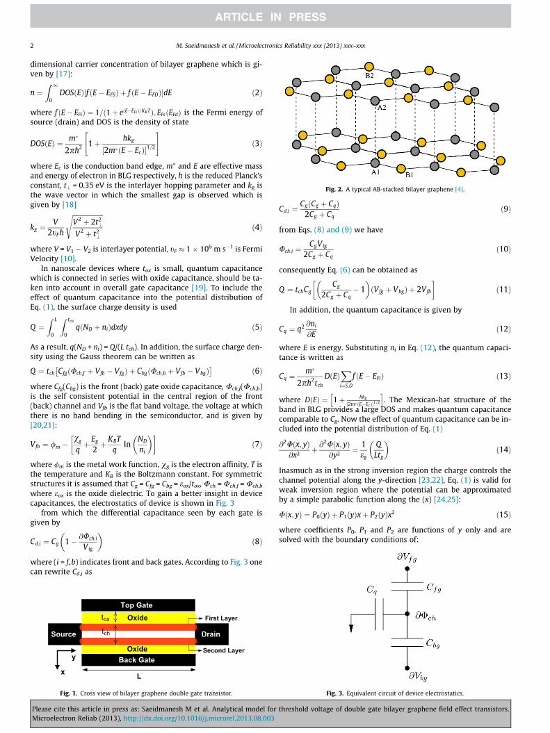
Fig. 2. A typical AB-stacked bilayer graphene [4].
2 M. Saeidmanesh et al. / Microelectronics Reliability xxx (2013) xxx–xxx
dimensional carrier concentration of bilayer graphene which is gi-ven by [17]:
n ¼Z 1
0DOSðEÞ½f ðE� EFSÞ þ f ðE� EFDÞ�dE ð2Þ
where f ðE� EFiÞ ¼ 1=ð1þ eðE�EFiÞ=KBTÞ; EFsðEFdÞ is the Fermi energy ofsource (drain) and DOS is the density of state
DOSðEÞ ¼ m�
2p�h2 1þ �hkg
2m�ðE� EcÞ½ �1=2
" #ð3Þ
where Ec is the conduction band edge, m⁄ and E are effective massand energy of electron in BLG respectively, �h is the reduced Planck’sconstant, t\ = 0.35 eV is the interlayer hopping parameter and kg isthe wave vector in which the smallest gap is observed which isgiven by [18]
kg ¼V
2tF�h
ffiffiffiffiffiffiffiffiffiffiffiffiffiffiffiffiffiffiffiV2 þ 2t2
?
V2 þ t2?
sð4Þ
where V = V1 � V2 is interlayer potential, tF � 1 � 106 m s�1 is FermiVelocity [10].
In nanoscale devices where tox is small, quantum capacitancewhich is connected in series with oxide capacitance, should be ta-ken into account in overall gate capacitance [19]. To include theeffect of quantum capacitance into the potential distribution ofEq. (1), the surface charge density is used
Q ¼Z L
0
Z tch
0qðND þ niÞdxdy ð5Þ
As a result, q(ND + ni) = Q/(L tch). In addition, the surface charge den-sity using the Gauss theorem can be written as
Q ¼ tch CfgðUch;f þ Vfb � VfgÞ þ CbgðUch;b þ Vfb � VbgÞ� �
ð6Þ
where Cfg(Cbg) is the front (back) gate oxide capacitance, Uch,f(Uch,b)is the self consistent potential in the central region of the front(back) channel and Vfb is the flat band voltage, the voltage at whichthere is no band bending in the semiconductor, and is given by[20,21]:
Vfb ¼ /m �vg
qþ Eg
2þ KBT
qln
ND
ni
� �� �ð7Þ
where /m is the metal work function, vg is the electron affinity, T isthe temperature and KB is the Boltzmann constant. For symmetricstructures it is assumed that Cg = Cfg = Cbg = eox/tox, Uch = Uch,f = Uch,b
where eox is the oxide dielectric. To gain a better insight in devicecapacitances, the electrostatics of device is shown in Fig. 3
from which the differential capacitance seen by each gate isgiven by
Cd;i ¼ Cg 1� @Uch;i
V ig
� �ð8Þ
where (i = f,b) indicates front and back gates. According to Fig. 3 onecan rewrite Cd,i as
Oxide
Source Drain
Top Gatetox
OxideBack Gate
x
y
tch
L
Second Layer
First Layer
Fig. 1. Cross view of bilayer graphene double gate transistor.
Please cite this article in press as: Saeidmanesh M et al. Analytical model forMicroelectron Reliab (2013), http://dx.doi.org/10.1016/j.microrel.2013.08.003
Cd;i ¼CgðCg þ CqÞ
2Cg þ Cqð9Þ
from Eqs. (8) and (9) we have
Uch;i ¼CgVig
2Cg þ Cqð10Þ
consequently Eq. (6) can be obtained as
Q ¼ tchCgCg
2Cg þ Cq� 1
� �ðVfg þ VbgÞ þ 2Vfb
� �ð11Þ
In addition, the quantum capacitance is given by
Cq ¼ q2 @ni
@Eð12Þ
where E is energy. Substituting ni in Eq. (12), the quantum capaci-tance is written as
Cq ¼m�
2p�h2tch
DðEÞXi¼S;D
f ðE� EFiÞ ð13Þ
where DðEÞ ¼ 1þ �hkg
2m�ðE�EcÞ½ �1=2
h i. The Mexican-hat structure of the
band in BLG provides a large DOS and makes quantum capacitancecomparable to Cg. Now the effect of quantum capacitance can be in-cluded into the potential distribution of Eq. (1)
@2Uðx; yÞ@x2 þ @
2Uðx; yÞ@y2 ¼ 1
eg
QLtg
� �ð14Þ
Inasmuch as in the strong inversion region the charge controls thechannel potential along the y-direction [23,22], Eq. (1) is valid forweak inversion region where the potential can be approximatedby a simple parabolic function along the (x) [24,25]:
Uðx; yÞ ¼ P0ðyÞ þ P1ðyÞxþ P2ðyÞx2 ð15Þ
where coefficients P0, P1 and P2 are functions of y only and aresolved with the boundary conditions of:
Fig. 3. Equivalent circuit of device electrostatics.
threshold voltage of double gate bilayer graphene field effect transistors.
M. Saeidmanesh et al. / Microelectronics Reliability xxx (2013) xxx–xxx 3
Uð0; yÞ ¼ Uf ðyÞUðtch; yÞ ¼ UbðyÞdUðx; yÞ
dx
x¼0¼ eox
eg
Uf ðyÞ � V 0fgtox
dUðx; yÞdx
x¼tch
¼ eox
eg
V 0bg �UbðyÞtox
ð16Þ
where V 0fg ¼ Vfg � Vfb;V0bg ¼ Vbg � Vfb;Uf ðyÞðUbðyÞÞ is the potential
on front (back) channel surface. The coefficients Pi(i = 0, 1, 2) canbe determined by applying the boundary conditions of Eq. (16) inEq. (15)
P0ðyÞ ¼ Uf ðyÞ ð17aÞ
P1ðyÞ ¼eox
eg
Uf ðyÞ � V 0fgtox
ð17bÞ
P2ðyÞ ¼ð1þ Cg=CchÞV 0fg þ V 0bg � ð2þ Cg=CchÞUf ðyÞ
t2chð1þ 2Cch=CgÞ
ð17cÞ
where Cch = eg/tch. Substitution Eq. (17) in Eq. (15) one can obtainthe potential distribution in every point (x,y) of channel
Uðx; yÞ ¼ Uf ðyÞ þeox
eg
Uf ðyÞ � V 0fgtox
x
þð1þ Cg=CchÞV 0fg þ V 0bg � ð2þ Cg=CchÞUf ðyÞ
t2chð1þ 2Cch=CgÞ
x2 ð18Þ
The front surface potential, (x = 0), can be obtained by substitutingEq. (18) in Eq. (1)
@2Uf ðyÞ@2y
� aUf ðyÞ ¼ b ð19Þ
where
a ¼ 2ð2þ Cg=CchÞt2
chð1þ 2Cch=CgÞð20aÞ
b ¼ðQtch=LÞð1þ 2Cch=CgÞ � 2ð1þ Cg=CchÞV 0fg � 2V 0bg
t2chð1þ 2Cch=CgÞ
ð20bÞ
solving Eq. (19) with boundary conditions of Uf(0) = Vbi andUf(L) = Vbi + Vds, where Vbi = VTln (ND/ni) is the built-in potential ofthe channel-drain and channel-source junctions with VT = KBT/q asthermal voltage, the front gate surface potential along the channelcan be given by
Uf ðyÞ ¼ C1expðffiffiffiap
yÞ þ C2expð�ffiffiffiap
yÞ � ba
ð21Þ
where
0 5 100.2
0.25
0.3
0.35
0.4
0.45
0.5
0.55
0.6
L (nm)
Surfa
ce P
oten
tial (
V)
0 10.1
0.2
0.3
0.4
0.5
0.6
L (
Cq=3µF/cm2
Cq=5 µF/cm2
Cq=3
Cq=
L= 10 nm L= 20 n
Fig. 4. Surface potential along channel distance for different channel lengths and quantuthe calculated results from the analytical model are represented by the solid lines.
Please cite this article in press as: Saeidmanesh M et al. Analytical model forMicroelectron Reliab (2013), http://dx.doi.org/10.1016/j.microrel.2013.08.003
C1 ¼#S �#Sexpð
ffiffiffiap
LÞ � #D
expðffiffiffiap
LÞ � expð�ffiffiffiap
LÞð22aÞ
C2 ¼#Sexpð
ffiffiffiap
LÞ � #D
expðffiffiffiap
LÞ � expð�ffiffiffiap
LÞð22bÞ
#S ¼baþ Vbi ð22cÞ
#D ¼baþ Vbi þ VDS ð22dÞ
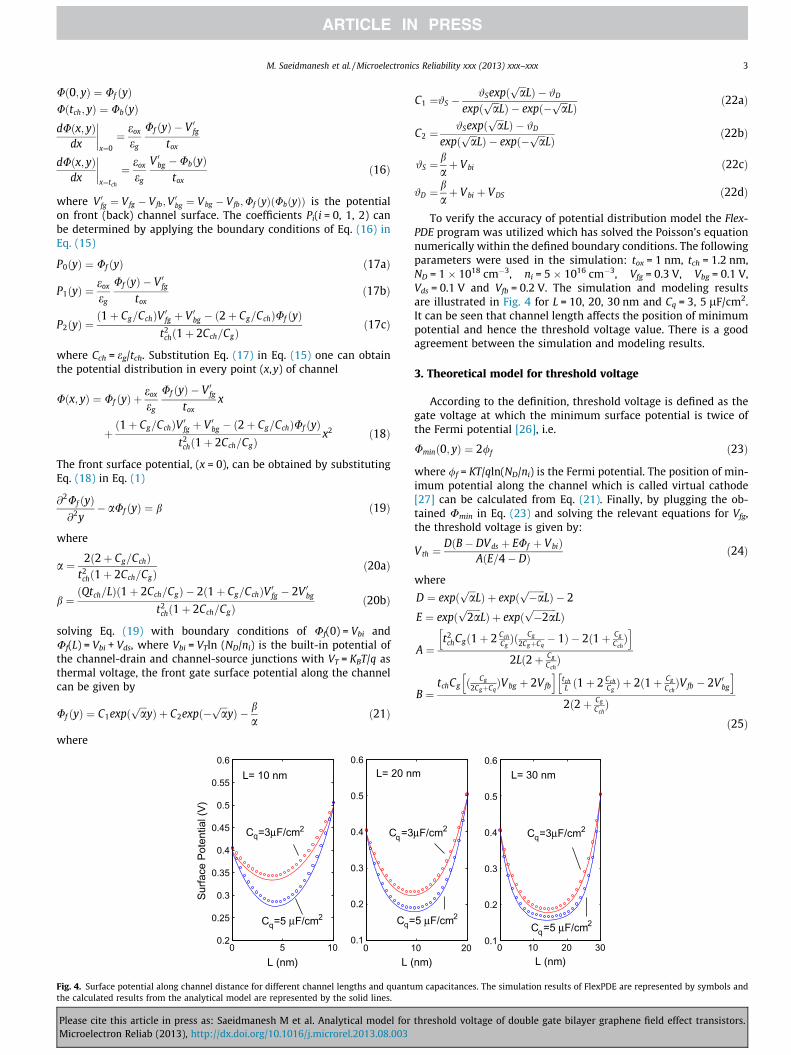
To verify the accuracy of potential distribution model the Flex-PDE program was utilized which has solved the Poisson’s equationnumerically within the defined boundary conditions. The followingparameters were used in the simulation: tox = 1 nm, tch = 1.2 nm,ND = 1 � 1018 cm�3, ni = 5 � 1016 cm�3, Vfg = 0.3 V, Vbg = 0.1 V,Vds = 0.1 V and Vfb = 0.2 V. The simulation and modeling resultsare illustrated in Fig. 4 for L = 10, 20, 30 nm and Cq = 3, 5 lF/cm2.It can be seen that channel length affects the position of minimumpotential and hence the threshold voltage value. There is a goodagreement between the simulation and modeling results.
3. Theoretical model for threshold voltage
According to the definition, threshold voltage is defined as thegate voltage at which the minimum surface potential is twice ofthe Fermi potential [26], i.e.
Uminð0; yÞ ¼ 2/f ð23Þ
where /f = KT/qln(ND/ni) is the Fermi potential. The position of min-imum potential along the channel which is called virtual cathode[27] can be calculated from Eq. (21). Finally, by plugging the ob-tained Umin in Eq. (23) and solving the relevant equations for Vfg,the threshold voltage is given by:
Vth ¼DðB� DVds þ EUf þ VbiÞ
AðE=4� DÞ ð24Þ
where
D ¼ expðffiffiffiap
LÞ þ expðffiffiffiffiffiffiffi�ap
LÞ � 2
E ¼ expðffiffiffiffiffiffi2ap
LÞ þ expðffiffiffiffiffiffiffiffiffiffi�2ap
LÞ
A ¼t2
chCgð1þ 2 CchCgÞð Cg
2CgþCq� 1Þ � 2ð1þ Cg
CchÞ
h i2Lð2þ Cg
CchÞ
B ¼tchCg ð Cg
2CgþCqÞVbg þ 2Vfb
h itchL ð1þ 2 Cch
CgÞ þ 2ð1þ Cg
CchÞVfb � 2V 0bg
h i2ð2þ Cg
CchÞ
ð25Þ
0 20nm)
0 10 20 300.1
0.2
0.3
0.4
0.5
0.6
L (nm)
µF/cm2 Cq=3µF/cm2
5 µF/cm2Cq=5 µF/cm2
m L= 30 nm
m capacitances. The simulation results of FlexPDE are represented by symbols and
threshold voltage of double gate bilayer graphene field effect transistors.

0 5 10 15 200.2
0.3
0.4
0.5
0.6
0.7
Position in the Channel (nm)
Surfa
ce P
oten
tial (
V)
Vds=0 VVds=0.1 VVds=0.2 V
Fig. 5. Surface potential along channel distance for different values of drain–sourcevoltages with tox = 1 nm, ND = 1 � 1018 cm�3 and ni = 5 � 1016 cm�3.
5 10 15 200.15
0.2
0.25
0.3
0.35
L (nm)
Thre
shol
d Vo
ltage
(V)
tox=1 nm
tox=2 nm
tox=3 nm
Fig. 6. Threshold voltage versus channel length for different oxide thickness’s withVds = 0.1 V, ND = 1 � 1017 cm�3 and ni = 5 � 1016 cm�3.
5 10 15 200
0.1
0.2
0.3
0.4
L (nm)
Thre
shol
d Vo
ltage
(V)
ND=1e+017ND=5e+017ND=9e+017
Fig. 7. Threshold voltage versus channel length for different doping concentrationwith Vds = 0.1 V, tox = 1 nm and ni = 5 � 1016 cm�3.
5 10 15 200.2
0.25
0.3
0.35
0.4
L (nm)
Thre
shol
d Vo
ltage
(V)
Vds=0.05 VVds=0.1 VVds=0.15 V
Fig. 8. Threshold voltage versus channel length for different drain source voltageswith tox = 1 nm, ND = 1 � 1017 cm�3 and ni = 5 � 1016 cm�3.
4 M. Saeidmanesh et al. / Microelectronics Reliability xxx (2013) xxx–xxx
4. Results and discussion
We have analytically calculated potential distribution andthreshold voltage of double gate BLG-FETs for different doping con-centrations, drain–source voltages and structural dimensions. Aschannel length becomes shorter the depletion region increaseswhich produces a huge surface potential that decreases the barrierheight. This phenomena is depicted in Fig. 5 where surface poten-tial is plotted versus channel length with Vds as parameter. It can beseen that the minimum surface potential value and its location aredependent on the drain voltage which is a sign of drain inducedbarrier lowering (DIBL).
In Fig. 6 the variation of threshold voltage as a function of chan-nel length is illustrated for different gate-oxide thickness (tox). Itcan be seen that threshold voltage increases as tox increases. Thisis because of the fact that gate-oxide electric field increases as tox
decreases. Even for an invariant gate voltage this electric fieldincrement induces more charge near the interface by decrementof threshold voltage.
In Fig. 7 the variation of threshold voltage versus channel lengthis shown for different doping concentrations (ND). It is illustratedthat as ND increases the threshold voltage also increases. This isdue to the fact that source-channel barrier increases with ND incre-ment which results in threshold voltage increment. Also, it is ob-served that threshold voltage decreases as source–drain distance(channel length) reduces that is because of the increment of elec-tric field effect on depletion regions of source and drain junctions.
Please cite this article in press as: Saeidmanesh M et al. Analytical model forMicroelectron Reliab (2013), http://dx.doi.org/10.1016/j.microrel.2013.08.003
Finally, Fig. 8 shows the effect of drain–source voltage onthreshold voltage along the channel. It can be seen that the thresh-old voltage reduces as drain–source voltage increases, and the ef-fect of drain–source voltage is also more significant for thesource side of the channel which represents the DIBL.
5. Conclusions
An analytical expression has been presented for potential distri-bution and threshold voltage of double gate BLG-FETs taking intoaccount the effect of quantum capacitance in potential model.For sake of verification, the analytical results were compared withthe simulation results of FlexPDE and a good agreement has beendemonstrated. The results show that channel length, doping con-centration and drain voltage could be used to adjust the thresholdvoltage. However, it has been proven that channel length of lessthan 10 nm and doping concentration in the order of 1017 cm�3
are effective. In addition, drain–source voltage is effective for chan-nels with L < 10 nm. As doping in the order of 1017 cm�3 is difficultand device with dimensions of less than 10 nm is still hard tofabricate, it is concluded that adjusting the threshold voltage inBLG-FET using L, Vds and ND is not a flexible approach.
Acknowledgements
The authors thank the Research Management Centre (RMC) ofUniversiti Teknologi Malaysia (UTM) for providing excellent re-search environment in completing this work.
threshold voltage of double gate bilayer graphene field effect transistors.

M. Saeidmanesh et al. / Microelectronics Reliability xxx (2013) xxx–xxx 5
References
[1] International technology roadmap for semiconductors. <http://www.itrs.net/>.[2] Castro Neto AH, Guinea F, Peres NMR, Novoselov KS, Geim AK. The electronic
properties of graphene. Rev Mod Phys 2009;81:109–62. http://dx.doi.org/10.1103/RevModPhys.81.109.
[3] Novoselov KS, Morozov SV, Mohinddin TMG, Ponomarenko LA, Elias DC, YangR, Barbolina II, Blake P, Booth TJ, Jiang D, Giesbers J, Hill EW, Geim AK.Electronic properties of graphene. Phys Status Solidi (b) 2007;244(11).
[4] Nilsson J, Castro Neto AH, Guinea F, Peres NMR. Electronic properties of bilayerand multilayer graphene. Phys Rev B 2008;78:045405. http://dx.doi.org/10.1103/PhysRevB.78.045405.
[5] Gusynin VP, Sharapov SG. Unconventional integer quantum hall effect ingraphene. Phys Rev Lett 2005;95:146801. http://dx.doi.org/10.1103/PhysRevLett.95.146801.
[6] Oostinga JB, Heersche HB, Liu X, Morpurgo AF. Gate-induced insulating state inbilayer graphene devices. Nat Mater 2007;7(2):151–7.
[7] Katsnelson MI, Novoselov KS, Geim AK. Chiral tunnelling and the Klein paradoxin graphene. Nat Phys 2006;2:620–5. http://dx.doi.org/10.1038/nphys384.read. arXiv:arXiv:cond-mat/0604323.
[8] Zhang Y, Tang T-T, Girit C, Hao Z, Martin MC, Zettl A, Crommie MF, Shen YR,Wang F. Direct observation of a widely tunable bandgap in bilayer graphene.Nature 2009;(7248):820–3. doi:10.1038/nature08105.
[9] Ohta T, Bostwick A, Seyller T, Horn K, Rotenberg E. Controlling the electronicstructure of bilayer graphene. Science 2006;313(5789):951–4.
[10] Castro EV, Novoselov KS, Morozov SV, Peres NMR, dos Santos JMBL, Nilsson J,et al. Biased bilayer graphene: semiconductor with a gap tunable by theelectric field effect. Phys Rev Lett 2007;99:216802. http://dx.doi.org/10.1103/PhysRevLett.99.216802.
[11] Sako R, Tsuchiya H, Ogawa M. Influence of band-gap opening on ballisticelectron transport in bilayer graphene and graphene nanoribbon fets. IEEETrans Electron Dev 2011;58(10):3300–6. http://dx.doi.org/10.1109/TED.2011.2161992.
[12] Cheli M, Fiori G, Iannaccone G. A semianalytical model of bilayer-graphenefield-effect transistor. IEEE Trans Electron Dev 2009;56(12):2979–86. http://dx.doi.org/10.1109/TED.2009.2033419.
[13] Sano E, Otsuji T. Bandgap engineering of bilayer graphene for field-effecttransistor channels. Japanese J Appl Phys 2009;48:14–16. doi:10.1143/JJAP.48.091605.
[14] Schwierz F. Graphene transistors. Nat Nano 2010;5(7):487–96.[15] Lu CL, Chang CP, Huang YC, Chen RB, Lin ML. Influence of an electric field on
the optical properties of few-layer graphene with AB stacking. Phys Rev B2006;73:144427. http://dx.doi.org/10.1103/PhysRevB.73.144427.
Please cite this article in press as: Saeidmanesh M et al. Analytical model forMicroelectron Reliab (2013), http://dx.doi.org/10.1016/j.microrel.2013.08.003
[16] Imam MA, Osman MA, Osman AA. Threshold voltage model for deep-submicron fully depleted SOI MOSFETs with back gate substrate inducedsurface potential effects. Microelectron Reliab 1999;39(4):487–95. http://dx.doi.org/10.1016/S0026-2714(99)00012-8.
[17] Saeidmanesh M, Ahmadi M, Ghadiry M, Akbari E, Kiani M, Ismail R.Perpendicular electric field effect on bilayer graphene carrier statistic. JComput Theore Nanosci 2013;10(9):1975–8. http://dx.doi.org/10.1166/jctn.2013.3158.
[18] Nilsson J, Neto AHC, Guinea F, Peres NMR. Electronic properties of graphenemultilayers. Phys Rev Lett 2006;97:266801. http://dx.doi.org/10.1103/PhysRevLett.97.266801.
[19] Fang T, Konar A, Xing H, Jena D. Carrier statistics and quantum capacitance ofgraphene sheets and ribbons. Appl Phys Lett 2007;91(9):092109. http://dx.doi.org/10.1063/1.2776887. <http://link.aip.org/link/?APL/91/092109/1>.
[20] Song SM, Park JK, Sul OJ, Cho BJ. Determination of work function of grapheneunder a metal electrode and its role in contact resistance. Nano Lett2012;12(8):3887–92. http://dx.doi.org/10.1021/nl300266p. arXiv:http://pubs.acs.org/doi/pdf/10.1021/nl300266p, <http://pubs.acs.org/doi/abs/10.1021/nl300266p>.
[21] Svilii B, Jovanovi V, Suligoj T. Analytical models of front- and back-gatepotential distribution and threshold voltage for recessed source/drain UTB SOIMOSFETs. Solid-State Electron 2009;53(5):540–7. http://dx.doi.org/10.1016/j.sse.2009.03.002. <http://www.sciencedirect.com/science/article/pii/S0038110109000537>.
[22] Chen Q, Meindl JD. Nanoscale metaloxidesemiconductor field-effecttransistors: scaling limits and opportunities. Nanotechnology2004;15(10):S549.
[23] Taur Y. Analytic solutions of charge and capacitance in symmetric andasymmetric double-gate MOSFETs. IEEE Trans Electron Dev2001;48(12):2861–9. http://dx.doi.org/10.1109/16.974719.
[24] Young K. Short-channel effect in fully depleted SOI MOSFETs. IEEE TransElectron Dev 1989;36(2):399–402. http://dx.doi.org/10.1109/16.19942.
[25] Yan R-H, Ourmazd A, Lee K. Scaling the Si MOSFET: from bulk to SOI to bulk.IEEE Trans Electron Dev 1992;39(7):1704–10. http://dx.doi.org/10.1109/16.141237.
[26] Bhattacherjee S, Biswas A. Modeling of threshold voltage and subthresholdslope of nanoscale DG MOSFETs. Semicond Sci Technol 2008;23(1):015010.
[27] Chen Q, Harrell I, EM, Meindl J. A physical short-channel threshold voltagemodel for undoped symmetric double-gate MOSFETs. IEEE Trans Electron Dev2003;50(7):1631–7. http://dx.doi.org/10.1109/TED.2003.813906.
threshold voltage of double gate bilayer graphene field effect transistors.