Embed Size (px)
Citation preview

Analysis of Power Distribution Network in Glass,
Silicon Interposer and PCB
Youngwoo Kim, Kiyeong Kim Jonghyun Cho, and
Joungho Kim
Department of Electrical Engineering,
KAIST
Daejeon, South Korea
Venky Sundaram and Rao Tummala
3D Systems Packaging Research Center
Georgia Institute of Technology
Atlanta, GA 30332, USA
Abstract—3D integration using a glass interposer and
through glass via technologies is expected to improve the
performance of a whole system significantly. However, due to the
high quality factor of the glass substrate, the sharp impedance
peaks on the Power Distribution Networks arise at the
resonances. When the mode resonances occur, performance of a
whole system could be degraded. Segmentation based impedance-
estimation was used to analyze the PDN impedance and analyzed
system degradation at resonance frequencies. To maximize
advantages of the glass interposers, the PDN should be carefully
designed to suppress the resonances. Considering the current
status of the glass fabrication processes, we propose that placing
the ground vias near the signal vias is the most promising
solution for maximizing the advantages of the glass interposers.
Keywords—interposer; PDN; glass; silicon; pcb; resonance,
segmentation method
I. INTRODUCTION
Recently, semiconductor industries have difficulties to
overcome technical challenges associated with the
performance saturation and limitation of CMOS technologies.
3D-Integration is expected to be the next generation solution
for system integration to achieve higher electrical performance
and at the same time reducing size of the whole systems.
However, it is still difficult to produce 3D products due to low
yield and high cost. Because these factors are critical to the
companies and customers, a new packaging technology using
an interposer, so called 2.5D integration is proposed. In the
2.5D integration, an interposer which is an interconnecting
medium is used to enable communication between various ICs
such as 3D stacked DRAMs, RF sensors and processors.
Interposers must have finer line pitch compared to PCB/PKGs
to mount ICs more compactly and have more I/Os. Because of
these reasons 2.5D-ICs using an interposer have comparable
electrical performance and size to 3D-ICs.
For the interposer substrate, silicon was proposed because
CMOS process has the longest history thus most advanced
among the semiconductor processes. Therefore using silicon
as an interposer substrate can enable very fine metal routing.
However, silicon shows high insertion loss which can degrade
performance of the whole system at the high frequency due to
conductivity and additionally very high in cost resulting from
the fine on-chip metal processes. To overcome these
difficulties that hinder 2.5D integration, glass can be used for
the interposer substrates. Compared to silicon interposers
which are fabricated by processing the wafers, glass
interposers use large panel processes which has higher yield
[1]. Also glass has no conductivity which will result in low
insertion loss of the signal at the high frequency [2]. Even
though minimum metal width and space on the glass
interposer are larger than that of silicon, it is enough to be
used for the signal routing on both side of an interposer and
soon, they are expected to be smaller.
It is apparent that glass has many advantages, however to
take advantages of the glass over silicon and FR-4 used as a
conventional PCBs/PKGs substrate, careful electrical design is
required. When the signal passes through the substrate,
discontinuity in the return current path arises. Return current
of the signal flows through the parasitic capacitor formed
between the power and ground planes thus it is heavily
affected by the substrate materials. Due to the high Q-factor,
sharp impedance peaks are generated on the PDN at resonance
frequencies. When the resonances occur, signal quality of the
glass interposers could be worse than that of silicon
interposers. At the same time, noise could be coupled to the
P/G planes since the signal vias can operate as a switching
current source [3]. Fig.1 illustrates possible problems that
could arise at the mode resonances. Therefore the PDNs of
glass interposers should be carefully designed to suppress the
mode resonances.
Fig.1. Possible problems that could occur at resonance frequencies of 2.5D-IC
with double side glass interposer.
978-1-4799-5545-9/14/$31.00 ©2014 IEEE 470
In this paper, we compare the PDN self-impedance of the
glass, silicon interposer and PCB and correlate them with
insertion loss. At the mode resonances, signal quality of the
glass interposers and PCBs was severely degraded, which was
worse than that of silicon interposers. Additionally, at the
resonance frequencies, noise could be coupled to the
power/ground planes. The PDN impedance of glass, silicon
interposer and PCB are estimated and analyzed using the
segmentation method to reduce computational resources and
time. Based on analysis, resonance suppression methods are
proposed.
II. COMPARISON OF PDN IMPEDANCE BETWEEN GLASS,
SILICON INTERPOSER AND PCB
A. PDN Impedance estimation using a Segmentation-method
Appearance of the sharp impedance peaks on the PDNs at
the mode resonance frequencies depends on port locations. By
using the segmentation method, we can accurately estimate the
PDN impedance of an interposer with different port
configuration in short time [4]. To estimate the PDN
impedance of the glass, silicon interposers and PCBs, unit cell
of each structure should be modeled. Only difference between
three structures is the substrate material. Dielectric material
and dimensions are fixed to analyze the effect of material on
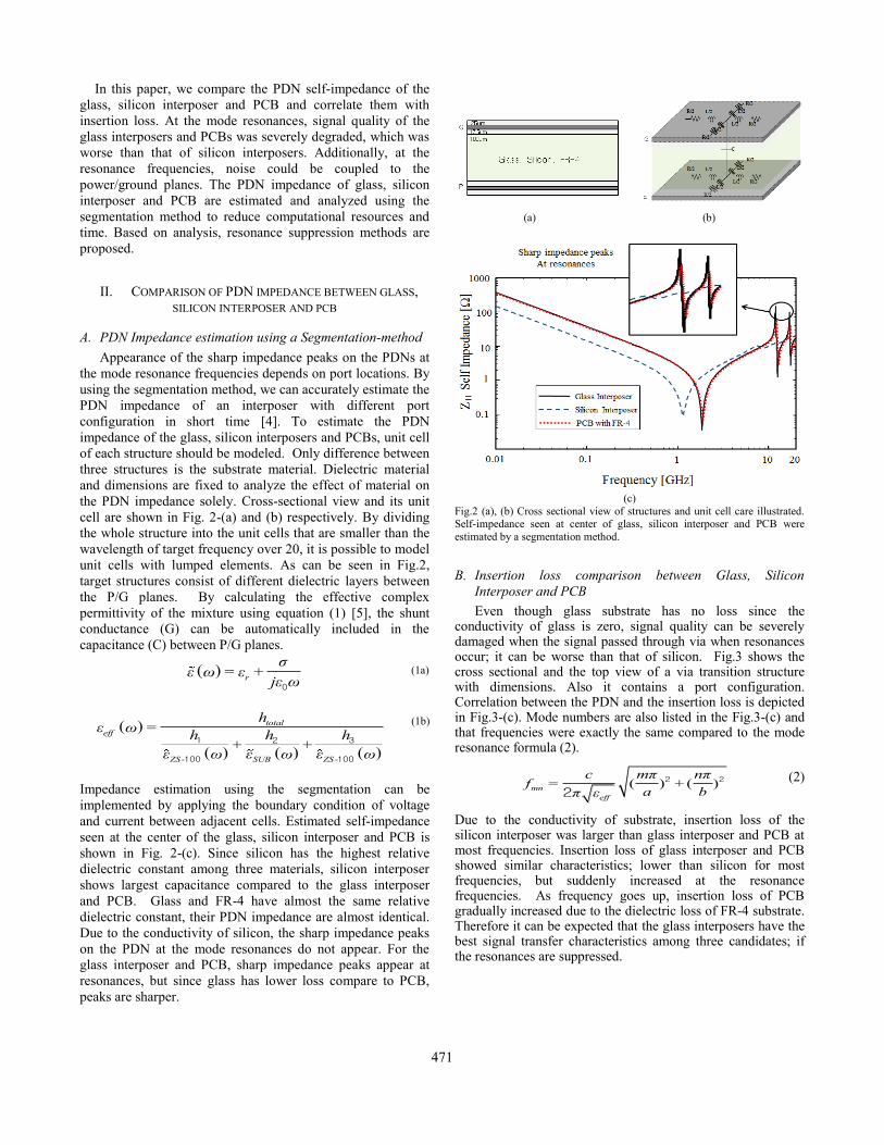
the PDN impedance solely. Cross-sectional view and its unit
cell are shown in Fig. 2-(a) and (b) respectively. By dividing
the whole structure into the unit cells that are smaller than the
wavelength of target frequency over 20, it is possible to model
unit cells with lumped elements. As can be seen in Fig.2,
target structures consist of different dielectric layers between
the P/G planes. By calculating the effective complex
permittivity of the mixture using equation (1) [5], the shunt
conductance (G) can be automatically included in the
capacitance (C) between P/G planes.
( ) = +r
σε ω ε
jε ω0
(1a)
( )
( ) ( ) ( )- -
=
+ +
total
eff
ZS SUB ZS
hε ω
h h h
ε ω ε ω ε ω1 2 3
100 100
(1b)
Impedance estimation using the segmentation can be
implemented by applying the boundary condition of voltage
and current between adjacent cells. Estimated self-impedance
seen at the center of the glass, silicon interposer and PCB is
shown in Fig. 2-(c). Since silicon has the highest relative
dielectric constant among three materials, silicon interposer
shows largest capacitance compared to the glass interposer
and PCB. Glass and FR-4 have almost the same relative
dielectric constant, their PDN impedance are almost identical.
Due to the conductivity of silicon, the sharp impedance peaks
on the PDN at the mode resonances do not appear. For the
glass interposer and PCB, sharp impedance peaks appear at
resonances, but since glass has lower loss compare to PCB,
peaks are sharper.
(a) (b)
(c)
Fig.2 (a), (b) Cross sectional view of structures and unit cell care illustrated. Self-impedance seen at center of glass, silicon interposer and PCB were
estimated by a segmentation method.
B. Insertion loss comparison between Glass, Silicon
Interposer and PCB
Even though glass substrate has no loss since the conductivity of glass is zero, signal quality can be severely damaged when the signal passed through via when resonances occur; it can be worse than that of silicon. Fig.3 shows the cross sectional and the top view of a via transition structure with dimensions. Also it contains a port configuration. Correlation between the PDN and the insertion loss is depicted in Fig.3-(c). Mode numbers are also listed in the Fig.3-(c) and that frequencies were exactly the same compared to the mode resonance formula (2).
= ( ) + ( )mn
eff
c mπ nπf
a bπ ε
2 2
2
(2)
Due to the conductivity of substrate, insertion loss of the silicon interposer was larger than glass interposer and PCB at most frequencies. Insertion loss of glass interposer and PCB showed similar characteristics; lower than silicon for most frequencies, but suddenly increased at the resonance frequencies. As frequency goes up, insertion loss of PCB gradually increased due to the dielectric loss of FR-4 substrate. Therefore it can be expected that the glass interposers have the best signal transfer characteristics among three candidates; if the resonances are suppressed.
471

(a) Cross sectional view (b) Top view
(c)
Fig.3 (a) Cross sectional view of via transition structure and (b) Top view is illustrated. Port configuration and dimensions are listed. Substrate thickness and polymer thickness are the same as Fig.2 (a). (c) Correlation between PDN impedance and insertion loss of each structure is illustrated. Numbers in parenthesis are mode resonance number. Frequencies where impedance peaks and insertion loss peaks appear well correlated.
C. Signal Quality comparison between glass, silicon
interposer and PCB at resonance frequencies and P/G
noise coupling
As can be seen in the section B, the signal quality can be severely distorted by the resonance. In this section, signal transfer characteristics were analyzed by using the eye diagram simulation. It is apparent that at the frequency where resonance does not appear, glass will show the best signal transfer characteristics. Therefore the eye diagrams were simulated at the data rate equal to certain resonance frequency to investigate how much resonance affects the signal. Also at that frequency, noise coupling voltage was observed at P/G planes. Simulation was carried out by applying PRBS signal with amplitude of 1V at port 1 and eye diagram was simulated at the port 2. Noise coupled to the P/G planes were observed at the port located at the side of each structure. Fig. 4 contains eye diagram and P/G noise of each structure at 26.6Gbps which corresponds to the mode (2,1) and (1,2) resonance’s frequency. It can be seen that at the resonance frequencies of a glass interposer and PCB, signal was distorted. Timing jitter of a glass interposer was 4ps (13.3% of UI), where the jitter of a silicon interposer was only 2ps (6.7% of UI). Also about 50mV to 70mV noise, which is about 5~7% of an input signal was coupled to the P/G planes. To maximize the advantages of the glass interposers, resonance suppression is crucial.
(a) Glass
(b) Silicon
(c) PCB
Fig. 4 Eye diagram and noise coupling through P/G planes were simulated at 26.6Gbps which corresponds to resonance frequency. (a) Glass interposer, (b) Silicon interposer, (c) PCB
III. SOLUTION FOR SUPPRESSING MODE RESONANCE OF
GLASS INTERPOSER
As can be seen in the Fig.3-(c), when the resonances occur, return current experience the high impedance. Also unwanted noise can be coupled to the PDNs. In 2.5D-ICs, various components are connected to the PDNs, therefore when the resonances occur, noise can be coupled to other components. To minimize the drawbacks of glass interposers, the PDNs should be designed to provide the return paths which have the low impedance. By placing decoupling capacitors or the ground vias near the signal vias, return current path discontinuity can be solved. However, placing the decoupling capacitors can solve many Power Integrity problems; it might not be the appropriate solution for the glass interposers’ resonance suppression. Decoupling capacitor pad sizes in glass interposer are still large. Due to this reason, the distance between the power and ground pins of the decoupling capacitors increase which cannot provide appropriate return current path. Also, a decoupling capacitor itself generates another resonance. New impedance peak is generated on the PDN, at that frequency, unexpected signal loss can occur [3]. Fig5.-(a) shows a decoupling capacitor configuration: 0603 size decoupling capacitors with 10pF are placed 300um away from the signal vias. Fig5-(b) shows a simulation result of the PDN impedance and insertion loss of the glass interposer with and without four 10pF 0603 decoupling capacitors.
472

(a)
(b)
Fig5. (a) Shows a top view of glass interposer with four 10pF 0603 capacitors and (b) Insertion loss and Self-impedance are compared between glass interposer with and without decoupling capacitors.
As can be seen in the Fig5-(b), placing the 0603 decoupling
capacitors did not affect much on neither PDN impedance nor
insertion loss; only some peaks are shifted to the higher
frequency. Therefore we can conclude that placing the
decoupling capacitors might not be the suitable solution for
the glass interposer’s resonance problems. Another solution is placing the ground vias near the signal vias to provide the return current path with the low impedance. As can be seen in Fig. 6-(a), two ground vias were located 120um away from the signal vias. Fig. 6-(b) contains the PDN impedance and insertion loss of glass interposer simulated with and without ground vias. In Fig. 6-(c) and (d), eye diagram and P/G noise coupling of both cases are compared. By locating the ground vias near the signal vias suppressed the magnitude of the impedance peaks on the PDN at the resonances. Additionally, insertion loss at the resonances also decreased. As can be seen in Fig.6-(b) eye opening increased at 26.6Gpbs which is resonance frequency; 0.284V to 0.317V. Timing jitter decreased to 2ps (6.7%) which is half of 4ps (13.3%). Additionally, magnitude of noise coupled to P/G planes went down significantly. By placing the ground vias near signal vias, The P/G noise coupling decreased and signal quality was improved.
(a)
(b)
(c)
(d)
Fig.6 (a) Ground vias are located near signal vias to provide the return current path. Design rules were provided by Georgia Tech Packaging Research Center. (b) PDN impedance and insertion loss of glass interposer with and without ground vias are compared. For the glass interposer containing ground vias, it is simulated with ground of PCB connected to interposer. (c) Eye-diagram simulation results of glass interposer with and without ground vias near signal vias. (d) P/G noise coupling comparison
Therefore we can conclude placing the ground vias is the best solutions for suppressing the mode resonances of the glass interposers to maximize its advantages.
473

I. CONCLUSION
2.5D-Integration based on interposer and through via
technologies is promising solution to achieve high system
performance and reducing the size of a whole system. Usually
silicon is used as a substrate material of an interposer;
however it is expensive and suffers signal loss at the high
frequency. As an alternative, glass can be used as a substrate
material which can solve the problems of the silicon
interposers. However, due to the low loss of the glass substrate,
the return current suffers the high impedance at the resonance
frequencies. At the resonances of the glass interposers, signal
is distorted and noise can be coupled to other components
integrated on interposer via PDN. To maximize the advantages
of the glass interposers, placing the ground vias near the signal
vias is mandatory when designing the PDNs of glass
interposers.
ACKNOWLEDGMENT
This work was supported by International Collaborative R&D
Program (funded by the Ministry of Trade, Industry and
Energy (MKE, Korea) [N0000899, Glass interposer based RF
FEM for Next Generation Mobile Smart Phone] also we
would like to acknowledge the financial support from the
R&D Convergence Program of MSIP (Ministry of Science,
ICT and Future Planning) and ISTK (Korea Research Council
for Industrial Science and Technology) of Republic of Korea
(Grant B551179-12-04-00).
REFERENCES
[1] Venky Sundaram, Quio Chen, Yuya Suzuki, Gokul Kumar, Fuhan Liu,
and Rao Tummala, "Low-cost and low-loss 3D silicon interposer for high bandwidth logic-to-memory interconnections without TSV in the logic IC," Electronic Components and Technology Conference (ECTC), 2012 IEEE 62nd, pp.292,297, May29 2012-June 1 2012
[2] Vijay Sukumaran, Tapobrata Bandyopadhyay, Venky Sundaram, Rao Tummala, "Low-Cost Thin Glass Interposers as a Superior Alternative to Silicon and Organic Interposers for Packaging of 3-D ICs," IEEE Transactions on Components, Packaging and Manufacturing Technology, vol.2, no.9, pp.1426,1433, Sept. 2012
[3] J.Cho, Y.Kim and J.Kim, “Analysis of glass interposer PDN and proposal of PDN resonance suppression methods,” 3D Systems Integration Conference (3DIC), 2013 IEEE International, Oct 2-5 2013
[4] K. Kim, W.Lee, J.Kim, T.Song, J.Kim, J.S.Pak and J.Kim, “Analysis of power distribution network in TSV-based 3D-IC” Electrical Performance of Electronic Packaging and Systems (EPEPS), 2010 IEEE 19th ,pp177,180, October 25 2010 – October 27 2010
[5] E. Tuncer, Y.V. Serdyuk, and S.M.Gubanski, “Dielectric mixtures: Electrical properties and modeling,” IEEE Trans. Dielectric. Electr. Insul.,vol. 9, no. 5, pp. 809-828, Oct. 2002
474


![Highly textured silicon [111 ... - Solar-Tectic LLC · Highly textured silicon [111] crystalline thin-film on buffered soda-lime glass by e-beam evaporation Shane McMahona, Ashok](https://img.dokumen.tips/doc/110x75/600fc27a2a567a149c76fd98/highly-textured-silicon-111-solar-tectic-highly-textured-silicon-111-crystalline.jpg)