Embed Size (px)
Citation preview

Wright State University Wright State University
CORE Scholar CORE Scholar
Browse all Theses and Dissertations Theses and Dissertations
2007
Analysis of a Small-Signal Model of a PWM DC-DC Buck-Boost Analysis of a Small-Signal Model of a PWM DC-DC Buck-Boost
Converter in CCM Converter in CCM
Julie JoAnn Lee Wright State University
Follow this and additional works at: https://corescholar.libraries.wright.edu/etd_all
Part of the Electrical and Computer Engineering Commons
Repository Citation Repository Citation Lee, Julie JoAnn, "Analysis of a Small-Signal Model of a PWM DC-DC Buck-Boost Converter in CCM" (2007). Browse all Theses and Dissertations. 159. https://corescholar.libraries.wright.edu/etd_all/159
This Thesis is brought to you for free and open access by the Theses and Dissertations at CORE Scholar. It has been accepted for inclusion in Browse all Theses and Dissertations by an authorized administrator of CORE Scholar. For more information, please contact [email protected].

ANALYSIS OF SMALL-SIGNAL MODEL OF A PWMDC-DC BUCK-BOOST CONVERTER IN CCM.
A thesis submitted in partial fulfillment
of the requirements for the degree of
Master of Science in Engineering
By
Julie J. Lee
B.S.EE, Wright State University, Dayton, OH, 2005
2007
Wright State University

WRIGHT STATE UNIVERSITYSCHOOL OF GRADUATE STUDIES
August 17, 2007
I HEREBY RECOMMEND THAT THE THESIS PREPARED UNDER MYSUPERVISION BYJulie J. Lee ENTITLED Analysis of Small-Signal Model of a DC-DC Buck-Boost Converter in CCMBE ACCEPTED IN PARTIAL FULFILLMENT OF THE REQUIREMENTSFOR THE DEGREE OFMaster of Science in Engineering
Marian K. Kazimierczuk, Ph.D.Thesis Director
Fred D. Garber, Ph.D.Department Chair
Committee onFinal Examination
Marian K. Kazimierczuk, Ph.D.
Kuldip S. Rattan, Ph.D.
Ronald Riechers, Ph.D.
Joseph F. Thomas, Jr., Ph.D.Dean, School of Graduate Studies

Abstract
Lee, Julie J. M.S. Egr., Department of Electrical Engineering, Wright State University, 2007.Analysis of Small-Signal Model PWM DC-D Buck-Boost Converter in CCM.
The objective of this research is to analyze and simulate thepulse-width-modulated (PWM)
dc-dc buck-boost converter and design a controller to gain stability for the buck-boost con-
verter. The PWM dc-dc buck-boost converter reduces and/or increases dc voltage from one
level to a another level in devices that need to, at differenttimes or states, increase or decrease
the output voltage.
In this thesis, equations for transfer funtions for a PWM dc-dc open-loop buck-boost con-
verter operating in continuous-conduction-mode (CCM) arederived. For the pre-chosen de-
sign, the open-loop characterics and the step responses arestudied. The converter is simulated
in PSpice to validate the theoretical analysis. AC analysisof the buck-boost converter is per-
formed using theoretical values in MatLab and a discrete point method in PSpice. Three
disturbances, change in load current, input voltage, and duty cycle are examined using step
responses of the system. The step responses of the output voltage are obtained using MatLab
Simulink and validated using PSpice simulation.
Design and simulation of an integral-lead (type III) controller is chosen to reduce dc error
and gain stability. Equations for the integral-lead controller are given based on steady-state
and AC analysis of the open-loop circuit, with a design method illustrated. The designed
controller is implemented in the circuit, and the ac behavior of the system is presented.
Closed loop transfer fuctions are derived for the buck-boost converter. AC analysis of the
buck-boost converter is studied using both theoretical values and a discrete point method in
PSpice. The step responses of the output voltage due to step change in reference voltage, input
voltage and load current are presented. The design and the obtained transfer functions of the
PWM dc-dc closed-loop buck-boost converter are validated using PSpice.
iii

Contents
1 Introduction 1
1.1 Background . . . . . . . . . . . . . . . . . . . . . . . . . . . . . . . . . . . 1
1.2 Thesis Objectives . . . . . . . . . . . . . . . . . . . . . . . . . . . . . . . .2
2 Open-Loop Buck-Boost 3
2.1 Transfer Functions for Small-Signal Open-Loop Buck-Boost . . . . . . . . . 3
2.1.1 Open-Loop Input Control to Output Voltage Transfer Function . . . . 3
2.1.2 Open-Loop Input Voltage to Output Voltage Transfer Function . . . . 13
2.1.3 Open-Loop Input Impedance . . . . . . . . . . . . . . . . . . . . . . 15
2.1.4 Open-Loop Output Impedance . . . . . . . . . . . . . . . . . . . . . 21
2.2 Open-Loop Responses of Buck-Boost using MatLab and Simulink . . . . . . 23
2.2.1 Open-Loop Response due to Input Voltage Step Change . .. . . . . 23
2.2.2 Open-Loop Response due to Load Current Step Change . . .. . . . 28
2.2.3 Open-Loop Response due to Duty Cycle Step Change . . . . .. . . 30
2.3 Open-Loop Responses of Buck-Boost Using PSpice . . . . . . .. . . . . . 32
2.3.1 Open-Loop Response of Buck-Boost . . . . . . . . . . . . . . . . .32
2.3.2 Open-Loop Response due to Input Voltage Step Change . .. . . . . 34
2.3.3 Open-Loop Response due to Load Current Step Change . . .. . . . 34
2.3.4 Open-Loop Response due to Duty Cycle Step Change . . . . .. . . 36
iv

3 Closed Loop Response 38
3.1 Closed Loop Transfer Functions . . . . . . . . . . . . . . . . . . . . .. . . 38
3.1.1 Integral-Lead Control Circuit for Buck-Boost . . . . . .. . . . . . . 42
3.1.2 Loop Gain of System . . . . . . . . . . . . . . . . . . . . . . . . . . 51
3.1.3 Closed Loop Control to Output Voltage Transfer Function . . . . . . 53
3.1.4 Closed Loop Input to Output Voltage Transfer Function. . . . . . . 53
3.1.5 Closed Loop Input Impedance . . . . . . . . . . . . . . . . . . . . . 57
3.1.6 Closed Loop Output Impedance . . . . . . . . . . . . . . . . . . . . 62
3.2 Closed Loop Step Responses of Buck-Boost . . . . . . . . . . . . .. . . . . 65
3.2.1 Closed Loop Response due to Input Voltage Step Change .. . . . . 65
3.2.2 Closed Loop Response due to Load Current Step Change . .. . . . . 68
3.2.3 Closed Loop Response due to Reference Voltage Step Change . . . . 71
3.3 Closed Loop Step Responses using PSpice . . . . . . . . . . . . . .. . . . . 73
3.3.1 Closed Loop Response of buck-boost . . . . . . . . . . . . . . . .. 73
3.3.2 Closed Loop Response due to Input Voltage Step Change .. . . . . 74
3.3.3 Closed Loop Response due to Load Current Step Change . .. . . . 76
3.3.4 Closed Loop Response due to Reference Voltage Step Change . . . . 79
4 Conclusion 81
4.1 Contributions . . . . . . . . . . . . . . . . . . . . . . . . . . . . . . . . . . 81
4.2 Future Work . . . . . . . . . . . . . . . . . . . . . . . . . . . . . . . . . . . 82
Appendix A 83
References 86
v

List of Figures
2.1 Small-signal model of buck-boost. . . . . . . . . . . . . . . . . . .. . . . . 4
2.2 Block diagram of buck-boost. . . . . . . . . . . . . . . . . . . . . . . .. . 4
2.3 Small-signal model of buck-boost to determineTp the input control to output
voltage transfer function. . . . . . . . . . . . . . . . . . . . . . . . . . . .. 5
2.4 Theoretical open-loop magnitude Bode plot of input control to output voltage
transfer functionTp for a buck-boost. . . . . . . . . . . . . . . . . . . . . . 11
2.5 Open-loop phase Bode plot of input control to output voltage transfer function
Tp for a buck-boost with and without 1µs delay. . . . . . . . . . . . . . . . 11
2.6 Discrete point open-loop magnitude Bode plot of input control to output volt-
age transfer functionTp for a buck-boost. . . . . . . . . . . . . . . . . . . . 12
2.7 Discrete points open-loop phase Bode plot of input control to output voltage
transfer functionTp for a buck-boost. . . . . . . . . . . . . . . . . . . . . . 12
2.8 Small-signal model of the buck-boost to determine the input to output voltage
transfer functionMv the input to output function. . . . . . . . . . . . . . . . 13
2.9 Open-loop magnitude Bode plot of input to output voltagetransfer function
Mv for a buck-boost. . . . . . . . . . . . . . . . . . . . . . . . . . . . . . . 16
2.10 Open-loop phase Bode plot of input to output transfer functionMv for a buck-
boost. . . . . . . . . . . . . . . . . . . . . . . . . . . . . . . . . . . . . . . 16
vi

2.11 Open-loop magnitude Bode plot of input to output transfer functionMv for a
buck-boost. . . . . . . . . . . . . . . . . . . . . . . . . . . . . . . . . . . . 17
2.12 Open-loop phase Bode plot of input to output transfer functionMv for a buck-
boost. . . . . . . . . . . . . . . . . . . . . . . . . . . . . . . . . . . . . . . 17
2.13 Open-loop magnitude Bode plot of input impedance transfer functionZi for a
buck-boost. . . . . . . . . . . . . . . . . . . . . . . . . . . . . . . . . . . . 19
2.14 Open-loop phase Bode plot of input impedance transfer functionZi for a buck-
boost . . . . . . . . . . . . . . . . . . . . . . . . . . . . . . . . . . . . . . . 19
2.15 Discrete points open-loop magnitude Bode plot of inputimpedance transfer
functionZi for a buck-boost. . . . . . . . . . . . . . . . . . . . . . . . . . . 20
2.16 Discrete points open-loop phase Bode plot of input impedance transfer func-
tion Zi for a buck-boost. . . . . . . . . . . . . . . . . . . . . . . . . . . . . 20
2.17 Small-signal model of the buck-boost for determining output impedanceZo. 21
2.18 Open-loop magnitude Bode plot of output impedance transfer functionZo for
a buck-boost. . . . . . . . . . . . . . . . . . . . . . . . . . . . . . . . . . . 24
2.19 Open-loop phase Bode plot of output impedance transferfunction Zo for a
buck-boost . . . . . . . . . . . . . . . . . . . . . . . . . . . . . . . . . . . . 24
2.20 Discrete points open-loop magnitude Bode plot of output impedance transfer
functionZo for a buck-boost. . . . . . . . . . . . . . . . . . . . . . . . . . . 25
2.21 Discrete points open-loop phase Bode plot of output impedance transfer func-
tion Zo for a buck-boost . . . . . . . . . . . . . . . . . . . . . . . . . . . . . 25
2.22 Open-Loop step response due to step change in input voltagevi. . . . . . . . 28
2.23 Open-Loop step response due to step change in load current io. . . . . . . . 30
2.24 Open-Loop step response due to step change in duty cycled. . . . . . . . . . 32
2.25 Open-loop buck-boost model with disturbances. . . . . . .. . . . . . . . . 33
2.26 Open-loop buck-boost response without disturbances.. . . . . . . . . . . . 33
vii

2.27 PSpice model of Open-Loop buck-boost with step change in input voltage. . 34
2.28 Open-Loop step response due to step change in input voltage using PSpice. . 35
2.29 PSpice model of Open-Loop buck-boost with step change in load current. . . 35
2.30 Open-Loop step response due to step change in load current using PSpice. . 36
2.31 PSpice model of Open-Loop buck-boost with step change in duty cycle. . . . 37
2.32 Open-Loop step response due to step change in duty cycleusing PSpice. . . 37
3.1 Closed loop circuit of voltage controlled buck-boost with PWM. . . . . . . . 39
3.2 Closed loop small-signal model of voltage controlled buck-boost. . . . . . . 39
3.3 Block diagram of a closed-loop small-signal voltage controlled buck-boost. . 40
3.4 Simplified block diagram of a closed-loop small-signal voltage controlled buck-
boost. . . . . . . . . . . . . . . . . . . . . . . . . . . . . . . . . . . . . . . 40
3.5 Magnitude Bode plot of modulator and input control to output voltage transfer
functionTmp for a buck-boost. . . . . . . . . . . . . . . . . . . . . . . . . . 43
3.6 Phase Bode plot of modulator and input control to output voltage transfer
functionTmp for a buck-boost. . . . . . . . . . . . . . . . . . . . . . . . . . 43
3.7 Magnitude Bode plot of the input control to output voltage transfer function
Tk before the compensator is added for a buck-boost. . . . . . . . . .. . . . 44
3.8 Phase Bode plot of the input control to output voltage transfer functionTk
before the compensator is added for a buck-boost. . . . . . . . . .. . . . . 44
3.9 The Integral Lead Controller . . . . . . . . . . . . . . . . . . . . . . .. . . 45
3.10 Magnitude Bode plot of the controller transfer function Tc for a buck-boost. . 52
3.11 Phase Bode plot of the controller transfer functionTc for a buck-boost. . . . 52
3.12 Magnitude Bode plot of the loop gain transfer functionT for a buck-boost. . . 54
3.13 Phase Bode plot of the loop gain transfer functionT for a buck-boost. . . . . 54
3.14 Magnitude Bode plot of the input control to output transfer functionTcl for a
buck-boost. . . . . . . . . . . . . . . . . . . . . . . . . . . . . . . . . . . . 55
viii

3.15 Phase Bode plot of the input control to output transfer functionTcl for a buck-
boost. . . . . . . . . . . . . . . . . . . . . . . . . . . . . . . . . . . . . . . 55
3.16 Magnitude Bode plot of the input control to output transfer functionTcl for a
buck-boost. . . . . . . . . . . . . . . . . . . . . . . . . . . . . . . . . . . . 56
3.17 Phase Bode plot of the input control to output transfer functionTcl for a buck-
boost. . . . . . . . . . . . . . . . . . . . . . . . . . . . . . . . . . . . . . . 56
3.18 Magnitude Bode plot of the input to output voltage transfer functionMvcl for
a buck-boost. . . . . . . . . . . . . . . . . . . . . . . . . . . . . . . . . . . 58
3.19 Phase Bode plot of the input to output voltage transfer function Mvcl for a
buck-boost. . . . . . . . . . . . . . . . . . . . . . . . . . . . . . . . . . . . 58
3.20 Magnitude Bode plot of the input to output voltage transfer functionMvcl for
a buck-boost. . . . . . . . . . . . . . . . . . . . . . . . . . . . . . . . . . . 59
3.21 Phase Bode plot of the input to output voltage transfer function Mvcl for a
buck-boost. . . . . . . . . . . . . . . . . . . . . . . . . . . . . . . . . . . . 59
3.22 Magnitude Bode plot of the input impedance transfer functionZicl for a buck-
boost. . . . . . . . . . . . . . . . . . . . . . . . . . . . . . . . . . . . . . . 63
3.23 Phase Bode plot of the input impedance transfer function Zicl for a buck-boost. 63
3.24 Magnitude Bode plot of the input impedance transfer functionZicl for a buck-
boost. . . . . . . . . . . . . . . . . . . . . . . . . . . . . . . . . . . . . . . 64
3.25 Phase Bode plot of the input impedance transfer function Zicl for a buck-boost. 64
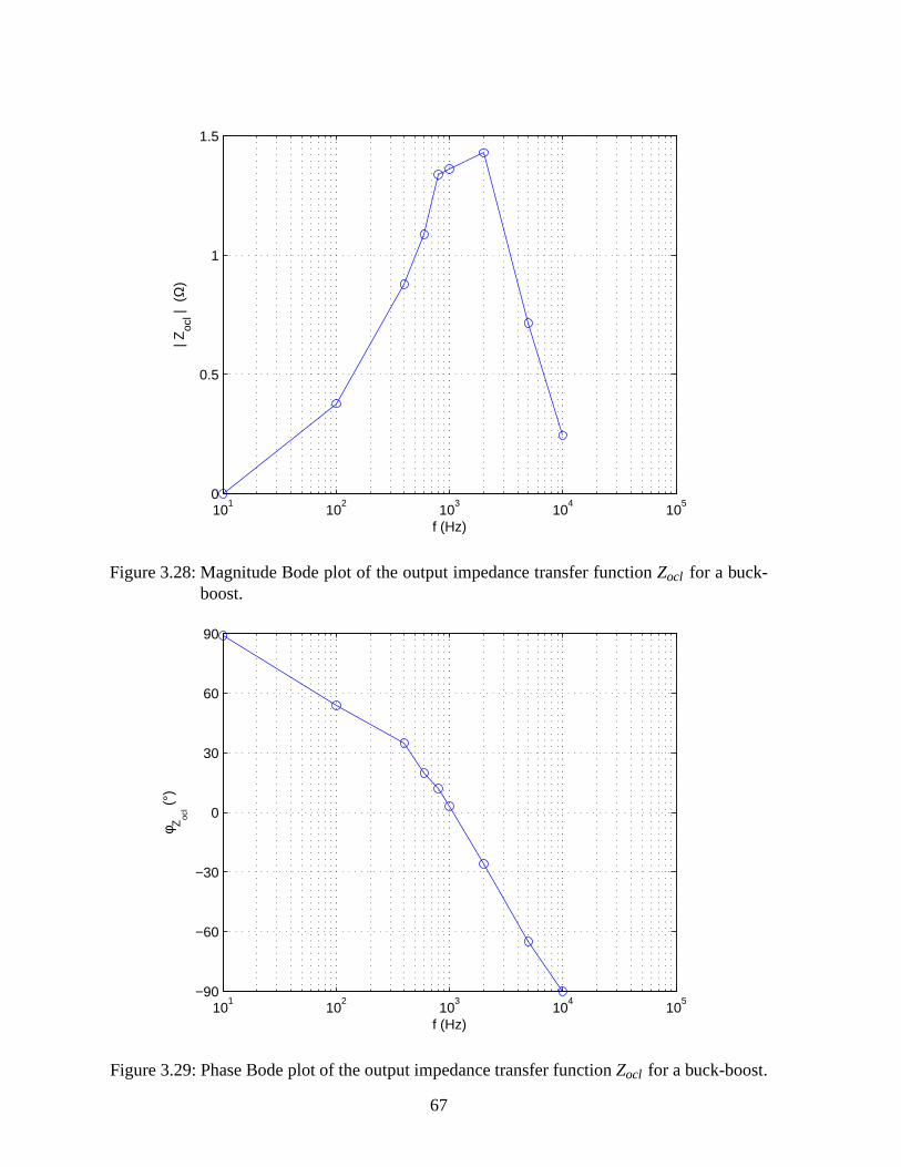
3.26 Magnitude Bode plot of the output impedance transfer function Zocl for a
buck-boost. . . . . . . . . . . . . . . . . . . . . . . . . . . . . . . . . . . . 66
3.27 Phase Bode plot of the output impedance transfer functionZocl for a buck-boost. 66
3.28 Magnitude Bode plot of the output impedance transfer function Zocl for a
buck-boost. . . . . . . . . . . . . . . . . . . . . . . . . . . . . . . . . . . . 67
3.29 Phase Bode plot of the output impedance transfer functionZocl for a buck-boost. 67
ix

3.30 Closed Loop step response due to step change invi. . . . . . . . . . . . . . . 69
3.31 Closed Loop step response due to step change inio. . . . . . . . . . . . . . . 71
3.32 Closed Loop step response due to step change invr. . . . . . . . . . . . . . 73
3.33 Closed loop buck-boost model with disturbances. . . . . .. . . . . . . . . . 74
3.34 Closed loop buck-boost response without disturbances. . . . . . . . . . . . . 75
3.35 PSpice model of Closed Loop buck-boost with step changein input voltage. 76
3.36 Closed Loop step response due to step change in input voltage using PSpice. 77
3.37 PSpice model of Closed Loop buck-boost with step changein load current. . 77
3.38 Closed Loop step response due to step change in load current using PSpice. . 78
3.39 PSpice model of Closed Loop buck-boost with step changein duty cycle. . . 79
3.40 Closed Loop step response due to step change in reference voltage using
PSpice. . . . . . . . . . . . . . . . . . . . . . . . . . . . . . . . . . . . . . 80
x

Acknowledgements
I would like to thank my advisor, Dr. Marian K. Kazimierczuk,for his guidance and input on
the thesis development process.
I also wish to thank Dr. Ronald Riechers and Dr. Kuldip S. Rattan for serving as members
of my MS thesis defense committee, giving the constructive criticism necessary to produce a
quality technical research document.
I would also like to thank the Department of Electrical Engineering and Dr. Fred D. Garber,
the Department Chair, for giving me the opportunity to obtain my MS degree at Wright State
University.

1 Introduction
1.1 Background
Trends in the current consumer electronics market demand smaller, more efficient devices.
With the increasing use of electronic devices on the market,a demand of low power and low
supply voltages is ever increasing. The key for power management is balancing need for
less power and lower supply voltages with maintaining operational ability. Many electronic
devices require several different voltages and are provided by either a battery or a rectified
ac supply line current. However, the voltage is usually not the required, or the ripple voltage
could be to high. Voltage regulator methodology is a constant dc voltage despite changes in
line voltage, load and temperature.
Voltage regulator can be classified into linear regulators and switching-mode regulators.
Some drawbacks of linear regulators are poor efficiency, which also leads to excess heat dis-
sipation and it is impossible to generate voltages higher than the supply voltage. Switching-
mode regulators can be separated into the following categories: Pulse-Width Modulated (PWM)
dc-dc regulators, Resonant dc-dc converters, and Switched-capacitor voltage regulators. The
PWM dc-dc regulators can be divided into three important topologies: buck converter, boost
converter, and buck-boost converter. The buck-boost converter is chosen for analysis.
The PWM dc-dc buck-boost converter reduces and increases dcvoltage from one level to
a another [1]-[5]. A buck-boost converter can operate in both continuous conduction mode
1

(CCM), which is the state discussed, and discontinuous conduction mode (DCM) depending
on the inductor current waveform. In CCM, the inductor current flows continuously for the
entire period, whereas in DCM, the inductor current reducesto zero and stays at zero for the
rest of the period before it begins to rise again.
1.2 Thesis Objectives
The objectives of this thesis are as follows:
1. To analyze and simulate the dc-dc buck-boost converter for open-loop.
2. To design a control circuit for the buck-boost converter.
3. To analyze and simulate the dc-dc buck-boost converter for closed-loop.
2

2 Open-Loop Buck-Boost
Derived small-signal open-loop transfer functions for theinput control to ouput voltage
transfer fuctionTp, audio susceptibilityMv, input impedanceZi and output impedanceZo. Us-
ing the transfer functions finding the AC analysis of the transfer fuction by finding the Bode
plots. Step responses of the system are found due to a step change in input voltagevi, duty
cycled and load currentio.
2.1 Transfer Functions for Small-Signal Open-Loop
Buck-Boost
2.1.1 Open-Loop Input Control to Output Voltage Transfer
Function
A small-signal open-loop buck-boost model is shown in Fig 2.1. A block diagram of a buck-
boost converter is shown in Fig 2.2. The MOSFET and diode are replaced by a small-signal
model of a switching network (dependent voltage and currentsources), the inductor is replaced
by a short and the capacitor is replaced by an open circuit. The pre-chosen measured values
of the circuit are:VI = 48 V, D = 0.407,VF = 0.7V, rDS = 0.4 Ω, RF = 0.02Ω, L = 334 mH,
C = 68µF, rC = 0.033Ω, andRL = 14Ω.
3

Z1
DilI dL
V dSD
D v − v( i o)
i l
RLio
rC
vo
+
−
vsd+
vi
−
−
+d
L
r
C
Z2
+
+
Figure 2.1: Small-signal model of buck-boost.
Z o
Mv
d
+
+
io
vi
vo’’ vo
Tp
vo’’’
vo’
Figure 2.2: Block diagram of buck-boost.
4

Di lI dL
V dSD
i l
rC
vsd+
Z1
−
d
L
r
C
RL vo
+
−
vi = 0
io= 0
i Z2
Dvsd Dvo= −
Z 2
−+
−+
Figure 2.3: Small-signal model of buck-boost to determineTp the input control to output volt-age transfer function.
The dependent sources are related to duty cycle. Setting theother two inputs to zero relates
the control input to the output. This transfer function due to duty cycle affecting the output is
Tp. The derivation using Fig 2.3 ofTp is below starting from first principles of KCL and KVL.
Finding the transfer function of the plantTp
iZ2 =vz2
Z2=
vo
Z2(2.1)
Using KCL
il + iZ2− Ild−Dil = 0
il (1−D)+ iZ2 − Ild = 0 (2.2)
ilZ1−VSDd −Dvsd = vo (2.3)
vsd = −vo (2.4)
ilZ1 = vo +VSDd −Dvo
5

il =vo(1−D)+ vsdd
Z1(2.5)
Substituting values
vo(1−D)+VSDdZ1
(1−D)+vo
Z2− ILd = 0 (2.6)
vo(1−D)2
Z1+
+VSDd(1−D)
Z1+
vo
Z2− ILd = 0
vo
[
(1−D)2
Z1+
1Z2
]
= d
[
IL −VSD(1−D)
Z1
]
Tp ≡vo(s)d(s)
|vo=io=0=
(
Il − VSD(1−D)Z1
)
(
(1−D)2
Z1+ 1
Z2
) =Il
(
1− VSD(1−D)IL
)
(1−D)2+ Z1Z2
(2.7)
Il =ID
(1−D)= − Io
(1−D)= − vo
(1−D)RL(2.8)
Using KVL
rIL −Dvsd + vF − vo = 0 (2.9)
vsd − vI − vF + vo = 0 ∴ vsd = vI + vF − vo (2.10)
Substituting values
r
[ −vo
(1−D)RL
]
−D(vI + vF − vo)+ vF − vo = 0 (2.11)
6

r
[ −vo
(1−D)RL
]
+DvF − o + vF − vo = DvI
−vo
[
r(1−D)Rl
− vID− vF
vo+1+D
(
vF
vo
)]
= vID
−vo
[
r(1−D)RL
+(1−D)
(
1− vF
vo
)]
= vID
vsd = vI + vF − vo = −vo
(
1− vF
vo− vI
vo
)
= ILRL(1−D)
(
1− vF
vo− 1
MV DC
)
vsd
IL=
1D
[
RL(1−D)
(
1+vF
|vo|+ r
)]
Tp(s) ≡vo
d|vi=io=0 =
IL
(
1− VSD(1−D)Il
)
(1−D)2+ Z1Z2
Tp(s) =IL
[
Z1− (1−D) vsdIL
]
Z1Z2
+(1−D)2
Tp(s) =IL
[
Z1− (1−D) vsdIL
]
Z1+(1−D)2Z2Z2
=IL
[
Z1− (1−D) vsdIL
]
Z2
Z1 +(1−D)2Z2(2.12)
Z1 = r + sL (2.13)
Z2 =RL(
rc + 1sC
)
RL + rC + 1sC
(2.14)
7

vsd
IL=
1D
[
RL(1−D)
(
1+vF
|vo|
)
+ r
]
(2.15)
IL =−vo
(1−D)RL(2.16)
Tp =IL
[
Z1− (1−D) vsdIL
]
Z2
Z1 +(1−D)2Z2(2.17)
DenTp = (r + sL)+(1−D)2 RL(
rc + 1sC
)
RL + rC + 1sC
DenTp =
(
RL + rC +1
sC
)
(r + sL)+(1−D)2RL
(
rc +1
sC
)
= RLr + rrC + r1
sC+ sLRL + sLrC +
LC
+(1−D)2(
RLrC +RL
sC
)
= sCRLr + sCrCr + r + s2CLRL + s2LCrC + sL+(1−D)2(sCRLrC +RL)
= s2+C[
r (RL + rC)+(1−D)2RLrC]
+L
LC (RL + rC)s+
r +(1−D)2RL
LC (RL + rC)(2.18)
NumTp = (sC)
[
1LC (RL + rC)
]
IL
[
RL(
rc + 1sC
)
RL + rC + 1sC
]
[
RL + rC +1
sC
][
Z1− (1−D)vsd
IL
]
= IL (RL(sCrC +1)(r + sL))− 1D
[
RL(1−D)2(
1+vF
|vo|+ r
)][
1LC (RL + rC)
]
8

=− Vo
(1−D)RL(RL(sCrC +1))
(
1LC(RL + rC)
)
(L)
[
s− 1DL
(
RL(1−D)2(1+vF
|vo|)+ r(1−2D)
)]
NumTp = − Vo
((1−D)RL + rC)
(
s+1
CrC
)[
s− 1DL
(RL(1−D)2(
1+vF
|vo|)+ r(1−2D)
)]
(2.19)
ζ =C[
r (RL + rC)+(1−D)2RLrC]
+L
2√
LC (RL + rC) [r +(1−D)2RL](2.20)
ωo =
√
r +(1−D)2RL
LC(RL + rC)(2.21)
ωzn = − 1CrC
(2.22)
ωzp =1
DL
[
RL(1−D)2(
1+vF
|vo|
)
+ r(1−2D)
]
(2.23)
Tp ≡vo
d|vi=io=0 = − V o
(1−D)(RL + rC)
(s+ωzn)(s+ωzp)
s2+2ζ ωos+ω2o
(2.24)
Tpx = − Vo
(1−D)(RL + rC)(2.25)
Tpo = Tp(0) =−VoR
(1−D)(RL + rC)
ωznωzp
ω2o
=VorC
(1−D)(RL + rC)
(
− 1CrC
)
1DL
(
RL(1−D)2(
1+ vF|vo|
)
+ r (1−2D))
r+(1−D)2RLLC(RL+rC)
9
=VorC
(1−D)(RL + rC)
(
RL(1−D)2(
1+vF|vo|
)
+r(1−2D))
CDLrC
r+(1−D)2RLLC(RL+rC)
Tpo =Vo
D(1−D)
RL(1−D)2(
1+ vF|vo|
)
+ r(1−2D)
r +(1−D)2RL
(2.26)
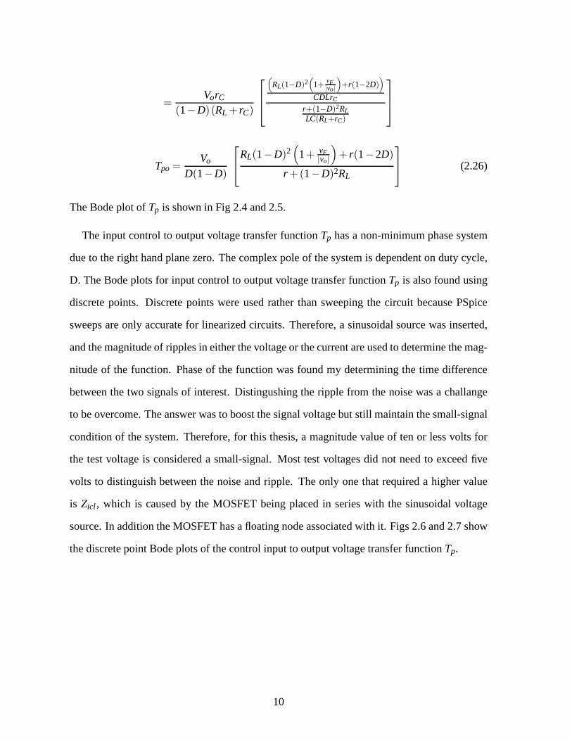
The Bode plot ofTp is shown in Fig 2.4 and 2.5.
The input control to output voltage transfer functionTp has a non-minimum phase system
due to the right hand plane zero. The complex pole of the system is dependent on duty cycle,
D. The Bode plots for input control to output voltage transfer functionTp is also found using
discrete points. Discrete points were used rather than sweeping the circuit because PSpice
sweeps are only accurate for linearized circuits. Therefore, a sinusoidal source was inserted,
and the magnitude of ripples in either the voltage or the current are used to determine the mag-
nitude of the function. Phase of the function was found my determining the time difference
between the two signals of interest. Distingushing the ripple from the noise was a challange
to be overcome. The answer was to boost the signal voltage butstill maintain the small-signal
condition of the system. Therefore, for this thesis, a magnitude value of ten or less volts for
the test voltage is considered a small-signal. Most test voltages did not need to exceed five
volts to distinguish between the noise and ripple. The only one that required a higher value
is Zicl, which is caused by the MOSFET being placed in series with thesinusoidal voltage
source. In addition the MOSFET has a floating node associatedwith it. Figs 2.6 and 2.7 show
the discrete point Bode plots of the control input to output voltage transfer functionTp.
10

100
101
102
103
104
105
−20
−10
0
10
20
30
40
50
f (Hz)
|Tp |
(dB
V)
Figure 2.4: Theoretical open-loop magnitude Bode plot of input control to output voltagetransfer functionTp for a buck-boost.
101
102
103
104
105
−90
−60
−30
0
30
60
90
120
150
180
f (Hz)
φ Tp (
°)
td = 0
td = 1µ s
Figure 2.5: Open-loop phase Bode plot of input control to output voltage transfer functionTp
for a buck-boost with and without 1µs delay.
11

101
102
103
104
105
−20
−10
0
10
20
30
40
50
f (Hz)
|Tp |
(dB
V)
Figure 2.6: Discrete point open-loop magnitude Bode plot ofinput control to output voltagetransfer functionTp for a buck-boost.
101
102
103
104
105
−90
−60
−30
0
30
60
90
120
150
180
f (Hz)
φ Tp (
°)
Figure 2.7: Discrete points open-loop phase Bode plot of input control to output voltage trans-fer functionTp for a buck-boost.
12
Z1
Di l
i l
r
vi
C
−
+
L
r
C=
Z2
vsd+ −
RL vo
+
−
+
Z i
Z 2ii i
D v − v( i o)
Dvsd
d = 0
io = 0
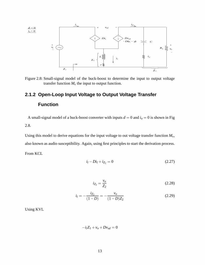
Figure 2.8: Small-signal model of the buck-boost to determine the input to output voltagetransfer functionMv the input to output function.
2.1.2 Open-Loop Input Voltage to Output Voltage Transfer
Function
A small-signal model of a buck-boost converter with inputsd = 0 andio = 0 is shown in Fig
2.8.
Using this model to derive equations for the input voltage toout voltage transfer functionMv,
also known as audio susceptibility. Again, using first principles to start the derivation process.
From KCL
il −Dil + iZ2 = 0 (2.27)
iZ2 =vo
Z2(2.28)
il = − iZ2
(1−D)= − vo
(1−D)Z2(2.29)
Using KVL
−ilZ1 + vo +Dvsd = 0
13

ilZ1 = vo +D(vi − vo)
ilZ1 = Dvi +(1−D)vo
− vo
Z2(1−D)Z1 = Dvi +(1−D)vo
Dvi = −(1−D)vo
[
1+Z1
Z2(1−D)2
]
Mv(s) ≡vo(s)vi(s)
|d=io=0 = − D
(1−D)[
1+ Z1Z2(1−D)2
]
= − D(1−D)
1
1+ Z1Z2(1−D)2
= − D(1−D)
(1−D)2
[
1
(1−D)+ Z1Z2
]
Mv =(1−D)DRLrC
L(RL + rC)
s+ωzn
s2 +2ζ ωos+ω2o
(2.30)
Mvx =(1−D)DRLrC
L(RL + rC)(2.31)
Mvo = Mv(0) = −(1−D)DRLrC
L(RL + rC)
ωzn
ω2o
= −(1−D)DRLrC
L(RL + rC)
1CrC
r+(1−D)2RLLC(RL+rC)
14

Mvo = − (1−D)DRL
r +(1−D)2RL(2.32)
Fig: 2.9 and 2.10 show the theoretical Bode plots ofMv.
Using PSpice to determine certain points of interest gives the following Bode plot shown in
figures 2.11 and 2.12.
2.1.3 Open-Loop Input Impedance
Finding the input impedanceZi for the open-loop buck-boost converter circuit. Using Fig
2.8 to derive the open-loop impedance of the buck-boost small-signal model.
Using KCL
Dil − il − iZ2 = 0
iZ2 = Dil − il
iZ2 = −(1−D)il (2.33)
From KVL
−Z1il +D(vi − vo)+ vo = 0
−Z1il +Dvio(1−D) = 0
−ilZ1+Dvi − il(1−D)(1−D)Z2 = 0
−ilZ1 +Dvi − il(1−D)2Z2 = 0
Dvi = il(Z1+(1−D)2Z2)
15

100
101
102
103
104
105
−90
−80
−70
−60
−50
−40
−30
−20
−10
0
10
f (Hz)
|Mv |
(dB
V)
Figure 2.9: Open-loop magnitude Bode plot of input to outputvoltage transfer functionMv fora buck-boost.
100
101
102
103
104
105
0
30
60
90
120
150
180
f (Hz)
φ MV
(°)
Figure 2.10: Open-loop phase Bode plot of input to output transfer functionMv for a buck-boost.
16

101
102
103
104
105
−90
−80
−70
−60
−50
−40
−30
−20
−10
0
10
f (Hz)
|Mv |
(dB
V)
Figure 2.11: Open-loop magnitude Bode plot of input to output transfer functionMv for abuck-boost.
101
102
103
104
105
0
30
60
90
120
150
180
f (Hz)
φ MV
(°)
Figure 2.12: Open-loop phase Bode plot of input to output transfer functionMv for a buck-boost.
17

Zi =vi
ii=
(Z1+(1−D)2Z2)
D2
=1
D2
[
r + sL+r +(1−D)2RL
LC(RL + rC)(1−D)2
]
=(r + sL)(RL + rC + 1
sC )+RL(rC + 1sC )(1−D)2
D2(RL + rC + 1sC )
=1
D2
[
rRL + rrC + rsC + sLRL + sLrC + L
C +RLrC(1−D)2+(1−D)2RLsC
RL + rC + 1sC
]
=1
D2
LC (RL + rC)s2+[
C(r(rC +RL)+RLrC(1−D)2)+L]
s+RL(1−D)2+ r
sCRL + sCrC +1
Zi =1
D2(LC (RL + rC))
(
s2+ C(r(RL+rC)+RLrC(1−D)2+LLC(RL+rC)
s+ RL(1−D)2+rLC(RL+rC)
)
sC (RL + rC)+1
where
ωrc =1
C(RL + rC)(2.34)
Zi =L
D2
s2+2ζ ωos+ω2o
s+ωrc(2.35)
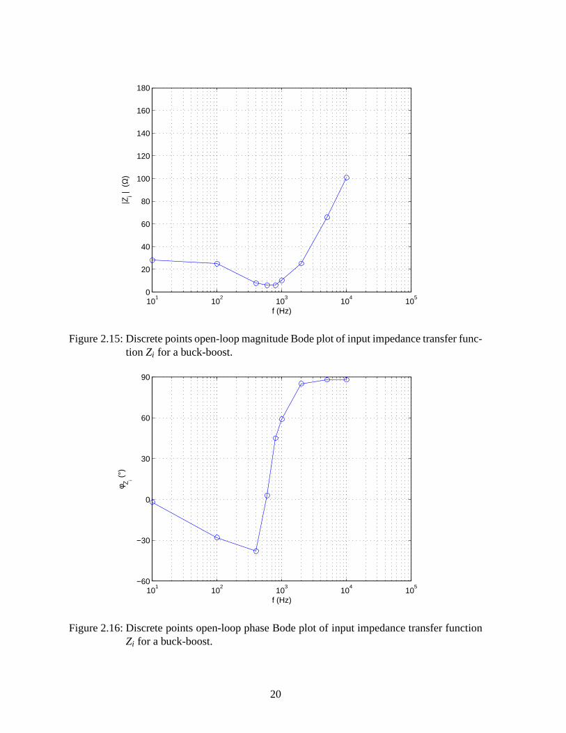
Figs: 2.13 and 2.14 show the theoretical Bode plots ofZi.
As shown above the Magnitude of|Zi| decreases quickly with an increase inD.
Figs 2.15 and 2.16 show the discrete point Bode plots forZi.
18

100
101
102
103
104
105
0
20
40
60
80
100
120
140
160
180
f (Hz)
|Zi|
(db
V)
Figure 2.13: Open-loop magnitude Bode plot of input impedance transfer functionZi for abuck-boost.
100
101
102
103
104
105
−60
−30
0
30
60
90
f (Hz)
φ Zi (
°)
Figure 2.14: Open-loop phase Bode plot of input impedance transfer functionZi for a buck-boost
19
101
102
103
104
105
0
20
40
60
80
100
120
140
160
180
f (Hz)
|Zi |
(Ω
)
Figure 2.15: Discrete points open-loop magnitude Bode plotof input impedance transfer func-tion Zi for a buck-boost.
101
102
103
104
105
−60
−30
0
30
60
90
f (Hz)
φ Zi (
°)
Figure 2.16: Discrete points open-loop phase Bode plot of input impedance transfer functionZi for a buck-boost.
20

Di l
i l
r
Z1
CL
r
C
Z2
+
vsd+ −
tvRL vo
+
−
Dvsd
−Dvo=
iZ2
it
Zo
ib
d = 0
vi = 0
io = 0
Figure 2.17: Small-signal model of the buck-boost for determining output impedanceZo.
2.1.4 Open-Loop Output Impedance
Solving for the transfer function of output impedanceZo. Output impedanceZo of the buck-
boost small-signal model is shown in Fig 2.17 where all threeinputsd, vi, andio equal 0. A
test voltagevt with a current ofit is applied to the output of the model. The ratio ofvt to it
determinesZo.
Using KVL
−Z1il −Dvt + vt = 0 (2.36)
il =(1−D)vt
Z1(2.37)
KCL
ib + iZ2 − it = 0
ib = (1−D)il (2.38)
21

(1−D)il = it − iZ2
(1−D)2vt
Z1= it −
vt
Z2
vt
(
c+1Z2
)
= it (2.39)
Zo =vt
it=
11
Z2+ (1−D)2
Z1
=Z1
Z1Z2
+(1+D)2
=
(r + sL)
(
RL(rC+ 1sC)
RL+rC+ 1sC
)
r + sL+RL(rC+ 1
sC)
RL+rC+ 1sC
(1−D)2
=(r + sL)
(
RL(
rC + 1sC
))
(r + sL)[
RL(
rC + 1sC
)]
+RL(1−D)2(
rC + 1sC
)
=1
LC(RL + rC)
s2 + CrRLrC+LRLLCRLrC
s+ rRLLCRLrC
s2+2ζ ωos+ω2o
Zo =1
LC(RL + rC)
(
s+ rL
)
(
s+ 1CrC
)
s2+2ζ ωos+ω2o
ωrL =rL
(2.40)
ωzn =1
CrC(2.41)
22

Zo ≡vt
it=
RLrC
(RL + rC)
(s+ωrL)(s+ωzn)
s2+2ζ ωos+ω2o
(2.42)
Figs: 2.18 and 2.19 show the Bode plots forZo.
As D increases so does the magnitude of|Zo|at low frequencies.
Figs: 2.18 and 2.19 show the discrete points PSpice simulated Bode plots forZo.
2.2 Open-Loop Responses of Buck-Boost using
MatLab and Simulink
2.2.1 Open-Loop Response due to Input Voltage Step Change
Response of output voltagevo due to a step change of 1 Volt in input voltagevi. The total
input voltage is given by equation 3.40 whereu(t) is the unit step function andVI(0−) is the
input voltage before applying the step voltage.
vI(t) = VI(0−)+4VIu(t) (2.43)
rearranging T_p open-loop input control to output voltage transfer function
M_v open-loop input to output voltage transfer function,audio suceptibility
Z_i open-loop input impedance transfer function
Z_o open-loop output impedance transfer function
vi(t) = 4VIu(t) = vI(t)−VI(0−) (2.44)
Changing from time domain to s-domain
23

100
101
102
103
104
105
0
1
2
3
4
5
6
7
f (Hz)
|Zo| (
dB V
)
Figure 2.18: Open-loop magnitude Bode plot of output impedance transfer functionZo for abuck-boost.
100
101
102
103
104
105
−90
−60
−30
0
30
60
f (Hz)
φ Zo (
°)
Figure 2.19: Open-loop phase Bode plot of output impedance transfer functionZo for a buck-boost
24

101
102
103
104
105
0
1
2
3
4
5
6
7
f (Hz)
|Zo |
(Ω)
Figure 2.20: Discrete points open-loop magnitude Bode plotof output impedance transferfunctionZo for a buck-boost.
101
102
103
104
105
−90
−60
−30
0
30
60
f (Hz)
φ Zo (
°)
Figure 2.21: Discrete points open-loop phase Bode plot of output impedance transfer functionZo for a buck-boost
25

vi(s) = Lvi(t) (2.45)
where the step change in s-domain is
vi(s) =4VI
s(2.46)
Therefore the transient response due to a step change invi becomes
vo(s) =v(s)
s(2.47)
= 4VIMvoω2
0
ωzn
s+ωzn
s(s2+2ζ ωos+ω2o )
= 4VIMvxs+ωzn
s(s2+2ζ ωos+ω2o )
(2.48)
Returning from s-domain to time domain
vo(t) = Lvo(s) (2.49)
producing the magnitude of the transient response is
= 4VIMvo
1+
√
1− 2ζ ωo
ωzn+
(
ωo
ωzn
)2 e−σt√
1−ζ 2sin(ωdt +φ)
(2.50)
Where
φ = tan−1
ωd
ωzn
(
1− ζωoωzn
)
+ tan−1
(
√
1−ζ 2
ζ
)
(2.51)
The total output voltage response is
vo(t) = V (0−)+ vo(t) t ≥ 0 (2.52)
26

The maximum overshoot defined in equation wherevo(∞) is the steady state value of the
output voltage.
Smax =vomax − vo(∞)
vo(∞)(2.53)
Obtaining the derivative for equation and setting it equal to zero produces the time instants at
which the maximum ofvo occurs
vomax = 4VIMvo
1+
√
1− 2ζ ωo
ωzn+
(
ωo
ωzn
)2 e−πζ√
1−ζ 2
(2.54)
Therefore the maximum overshoot is
Smax =
√
1− 2ζ ωo
ωzn+
(
ωo
ωzn
)2 e−πζ√
1−ζ 2(2.55)
The maximum relative transient ripple of the total output voltage can be defined as
δmax =vomax − vo(∞)
vo(∞)(2.56)
wherevo(∞) is defined as the steady state value of the output voltage. Given the measured
values of the circuit are:VI = 48 V, D = 0.407,VF = 0.7 V, rDS = .4 Ω, RF = 0.02 Ω, L =
334 mH,C = 68µF, rC = 0.033Ω, andRL = 14Ω. These values lead to a maximum overshoot
, Smax = 35.67% and a relative transient rippleδmax = 1.05%.
The step change due tovi is shown in Fig: 2.22 .
27

0 1 2 3 4 5
−28.8
−28.7
−28.6
−28.5
−28.4
−28.3
−28.2
−28.1
−28
t (ms)
v O (
V)
Figure 2.22: Open-Loop step response due to step change in input voltagevi.
2.2.2 Open-Loop Response due to Load Current Step Change
Response ofvo due to a step change of .1 Amp inio. The total load current is given
by equation 3.40 whereu(t) is the unit step function andIo(0−) is the input current before
applying the step current.
Io(t) = Io(0−)+4Iou(t) (2.57)
Step change in the time domain is
io(t) = io(t)− Io(0−) = 4Iou(t) (2.58)
28
Changing from time domain into s-domain the step change becomes
io(s) =4Io
s(2.59)
The transient component of the output voltage is
vo(s) = Zo(s)io(s) = −4IoRLrC
RL + rC
(s+ωzn)(s+ωrl)
s(s2+2ζ ωos+ω2o )
= −4 IoZox(s+ωzn)(s+ωrl)
s(s2+2ζ ωos+ω2o )
(2.60)
Switching back from s-domain to time domain
vo(t) = L−1vo(s) (2.61)
The total output voltage is
vo(t) = V (0−)+ vo(t) (2.62)
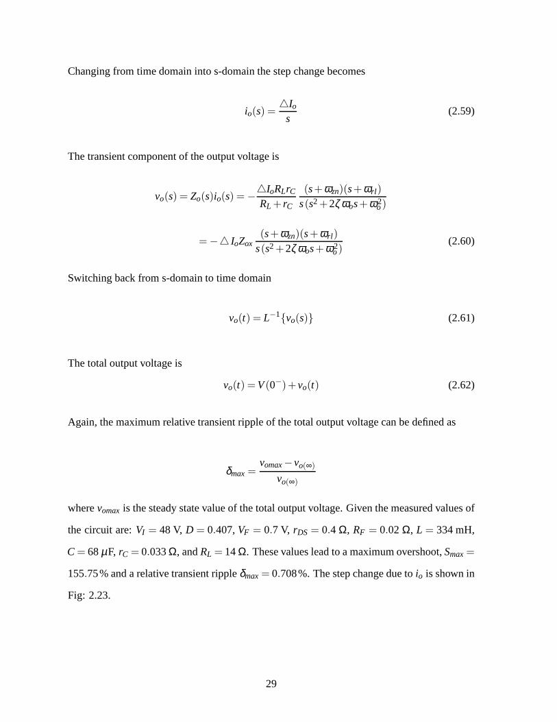
Again, the maximum relative transient ripple of the total output voltage can be defined as
δmax =vomax − vo(∞)
vo(∞)
wherevomax is the steady state value of the total output voltage. Given the measured values of
the circuit are:VI = 48 V, D = 0.407,VF = 0.7 V, rDS = 0.4 Ω, RF = 0.02 Ω, L = 334 mH,
C = 68µF, rC = 0.033Ω, andRL = 14Ω. These values lead to a maximum overshoot,Smax =
155.75% and a relative transient rippleδmax = 0.708%. The step change due toio is shown in
Fig: 2.23.
29

0 1 2 3 4 5−28.35
−28.3
−28.25
−28.2
−28.15
−28.1
−28.05
−28
t (ms)
v O (
V)
Figure 2.23: Open-Loop step response due to step change in load currentio.
2.2.3 Open-Loop Response due to Duty Cycle Step Change
The step response ofvo for a step change of 0.1 ind is given. The total duty cycle is given
by equation 3.40 whereu(t) is the unit step function and D is the duty cycle before applying
the step change in the duty cycle.
dT (t) = D+4dT u(t) (2.63)
The time domain step change in the duty cycle is
d(t) = dT (t)−D = 4dT u(t) (2.64)
30

leading to the s-domain version which is
d(s) =4dT
s(2.65)
The transient response of the output voltage of the open-loop buck-boost in s-domain is
vo(s) = Tp(s)d(s) =4dT Tp(s)
s
= −4dT Tpoω2
o
ωznωzp
(s+ωzn)(s−ωzp)
s(s2+2ζ ωos+ω2o )
(2.66)
Switching back from s-domain to time domain
vo(t) = L−1vo(s)
The total output voltage is
vo(t) = V (0−)+ vo(t)
Again, the maximum relative transient ripple of the total output voltage can be defined as
δmax =vomax − vo(∞)
vo(∞)
wherevomax is the steady state value of the total output voltage. Given the measured values of
the circuit are:VI = 48 V, D = 0.407,VF = 0.7 V, rDS = 0.4 Ω, RF = 0.02 Ω, L = 334 mH,
C = 68µF, rC = .033Ω, andRL = 14Ω. These values lead to a maximum overshoot,Smax =
36.01% and a relative transient rippleδmax = 10.16%. The step change due tod is shown in
Fig: 2.24 .
31

0 1 2 3 4 5
−42
−40
−38
−36
−34
−32
−30
−28
t (ms)
v O (
V)
Figure 2.24: Open-Loop step response due to step change in duty cycled.
2.3 Open-Loop Responses of Buck-Boost Using
PSpice
2.3.1 Open-Loop Response of Buck-Boost
A circuit showing the open-loop buck-boost is shown in Fig 2.25 and a model of this circuit is
shown in Fig 2.1. The measured values of the circuit are:VI = 48 V, D = 0.389,L = 334 mH,
C = 68µF, rC = 0.033Ω, rL = 0.32Ω andRL = 14Ω. An International Rectifier IRF150 power
MOSFET is selected, which has aVDSS = 100V , ISM = 40A, rDS = 55mΩ, Co = 100pF, and
Qg = 63nC. Also, an International Rectifier 10CTQ150 Schottky Common Cathode Diode is
selected with aVR = 100V, IF(AV ) = 10A,VF = 0.73V andRF = 28mΩ . The duty cycle for
the MOSFET changes from 0.407 to 0.389 to obtain the correct output of−28 V as predicted
using MatLab. Also the switching frequency forVp which controls the duty cycle is 100kHz
32

RL ioIV
vi
o
Vp
v
D
+L C
rL rC
Figure 2.25: Open-loop buck-boost model with disturbances.
0 1 2 3 4 5 6 7 8−40−38−36−34−32−30−28−26−24−22−20−18−16−14−12−10
−8−6−4−2
0
t (ms)
Vou
t (V
)
Figure 2.26: Open-loop buck-boost response without disturbances.
allowing for a fast response time. The disturbances to the system arevi, io andd.
The output voltage of the buck-boost without any disturbances can be seen in Fig 2.26 . The
maximum overshoot is 41.25 %, settling time within five percent of steady state value is 3ms,
and settling time withing one percent of steady state value is 7ms.
33

CVp
RLIV
vi
o
rL r
v
D
+L C
Figure 2.27: PSpice model of Open-Loop buck-boost with stepchange in input voltage.
2.3.2 Open-Loop Response due to Input Voltage Step Change
The PSpice circuit with step change in input voltage is shownin Fig 2.27. An additional
voltage pulse source of 1 volt was added with a delay of 10 ms, so that the circuit ran for
sufficient time to reach steady state value, and then the disturbance is activated. The output
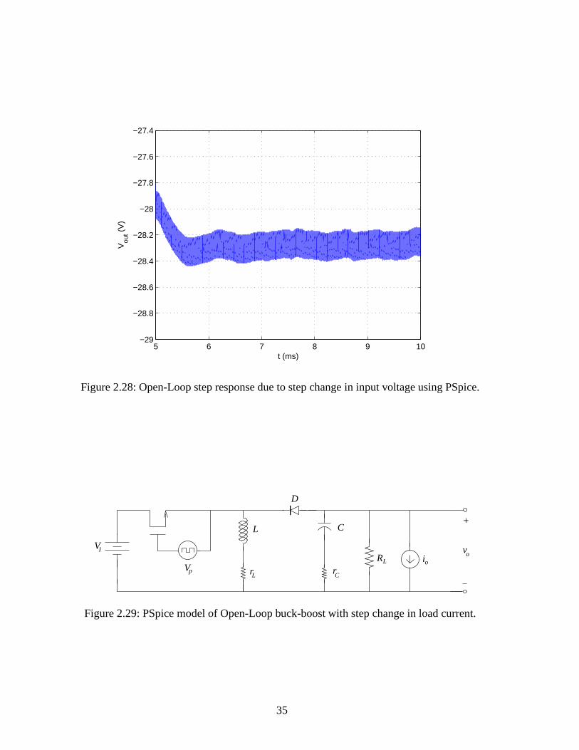
voltage of the buck boost can be seen in Fig 2.28. The voltage ripple is.22 volts contained be-
tween−27.33V and−27.55V, the average value of steady state is−27.425V. The maximum
overshoot isSmax = 21.74% and settling time within one percent is 2ms which contains the
ripple of steady state value. The relative maximum overshoot is δmax = 0.455%.
2.3.3 Open-Loop Response due to Load Current Step Change
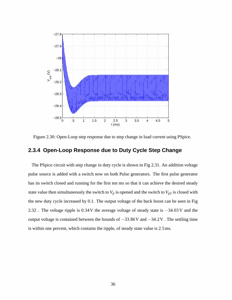
The PSpice circuit with step change in load current is shown in Fig 2.29. An additional
current pulse source of .1 Amp was added with a delay of 10 ms sothat the circuit ran for
sufficient time to reach steady state value, then the disturbance is activated. The output voltage
of the buck boost can be seen in Fig 2.30 . The voltage ripple is0.22V and the output voltage
is contained between−28.36V and−28.14V. the average value of steady state is−22.25V .
The maximum overshoot isSmax = 88% and settling time within one percent is 1.4ms which
contains the ripple of steady state value. The relative maximum overshoot isδmax = 0.779%.
34
5 6 7 8 9 10−29
−28.8
−28.6
−28.4
−28.2
−28
−27.8
−27.6
−27.4
t (ms)
Vou
t (V
)
Figure 2.28: Open-Loop step response due to step change in input voltage using PSpice.
CVp
RL ioo
rL r
v
D
+L C
VI
Figure 2.29: PSpice model of Open-Loop buck-boost with stepchange in load current.
35
0 .5 1 1.5 2 2.5 3 3.5 4 4.5 5−28.5
−28.4
−28.3
−28.2
−28.1
−28
−27.9
−27.8
t (ms)
Vou
t (V
)
Figure 2.30: Open-Loop step response due to step change in load current using PSpice.
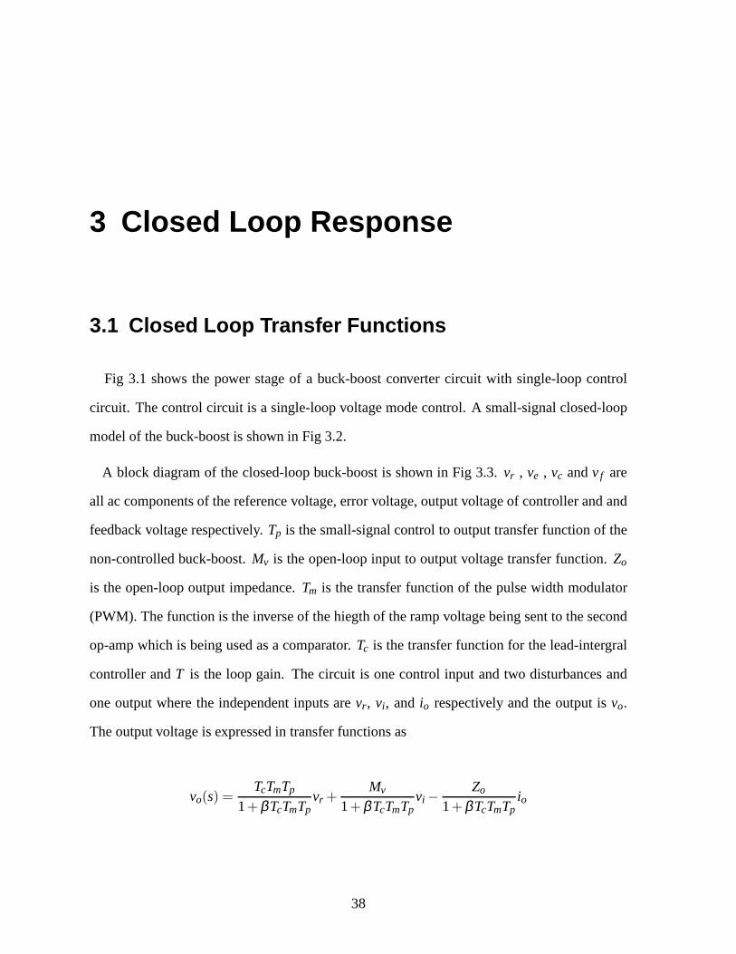
2.3.4 Open-Loop Response due to Duty Cycle Step Change
The PSpice circuit with step change in duty cycle is shown in Fig 2.31. An addition voltage
pulse source is added with a switch now on both Pulse generators. The first pulse generator
has its switch closed and running for the first ten ms so that itcan achieve the desired steady
state value then simultaneously the switch toVp is opened and the switch toVp2 is closed with
the new duty cycle increased by 0.1. The output voltage of thebuck boost can be seen in Fig
2.32 . The voltage ripple is 0.34V the average voltage of steady state is−34.03 V and the
output voltage is contained between the bounds of−33.86V and−34.2V . The settling time
is within one percent, which contains the ripple, of steady state value is 2.5ms.
36

CVp
RL
vo
rL r
V
+L C
Vp2
D
I
Figure 2.31: PSpice model of Open-Loop buck-boost with stepchange in duty cycle.
0 1 2 3 4 5 6−35
−34
−33
−32
−31
−30
−29
−28
−27
t (ms)
Vou
t (V
)
Figure 2.32: Open-Loop step response due to step change in duty cycle using PSpice.
37
3 Closed Loop Response
3.1 Closed Loop Transfer Functions
Fig 3.1 shows the power stage of a buck-boost converter circuit with single-loop control
circuit. The control circuit is a single-loop voltage mode control. A small-signal closed-loop
model of the buck-boost is shown in Fig 3.2.
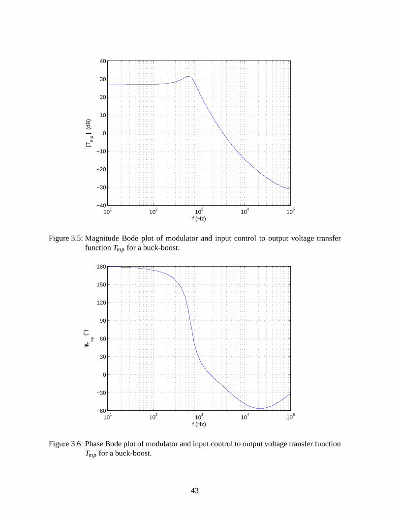
A block diagram of the closed-loop buck-boost is shown in Fig3.3. vr , ve , vc andv f are
all ac components of the reference voltage, error voltage, output voltage of controller and and
feedback voltage respectively.Tp is the small-signal control to output transfer function of the
non-controlled buck-boost.Mv is the open-loop input to output voltage transfer function.Zo
is the open-loop output impedance.Tm is the transfer function of the pulse width modulator
(PWM). The function is the inverse of the hiegth of the ramp voltage being sent to the second
op-amp which is being used as a comparator.Tc is the transfer function for the lead-intergral
controller andT is the loop gain. The circuit is one control input and two disturbances and
one output where the independent inputs arevr, vi, andio respectively and the output isvo.
The output voltage is expressed in transfer functions as
vo(s) =TcTmTp
1+βTcTmTpvr +
Mv
1+βTcTmTpvi −
Zo
1+βTcTmTpio
38

VV
+
+
++
+ +
RA
RB
vo
vo
vGS
RL io
+
+
L C
β
R
VI
vc
Z f
Zi
vAB
vt
iv
dTvE
vF
v
vI
++
+vF
Figure 3.1: Closed loop circuit of voltage controlled buck-boost with PWM.
I dL
i l
io
rC
vsd+
Z1
Di l
−
L
r
C
β+ +
+ T T d+
+
+vi−
+
vo
+
−
RL
Z2
V dSD
D v − v( i o)
ΖoclΖicl
ii
vf
RBRAvf vo
ve cv
vR
Figure 3.2: Closed loop small-signal model of voltage controlled buck-boost.
39

voTpTm Tc
β
vR
ve vc
vfα
d+ vo’
Z o
Mv
’’
io
vi
vo’’’
vo
Figure 3.3: Block diagram of a closed-loop small-signal voltage controlled buck-boost.
Z o
Mv+
+
io
vi
vo’’
vo’’’
vo’
vr
vo
A
1 +T1
Figure 3.4: Simplified block diagram of a closed-loop small-signal voltage controlled buck-boost.
=A
1+Tvr +
Mv
1+Tvi −
Zo
1+Tio = Tclvr +Mvclvi −Zocl io (3.1)
WhereA = TcTmTp andT = βA
PWM transfer function is expressed
40

Tm ≡ d(s)vc(s)
=1
VT m(3.2)
WhereVT m is peak value of the triangular pulse.
CombiningTm andTp together, the control to output transfer function is produced giving a
new functionTmp, given by
Tmp(s) = Tm(s)Tp(s) =vorC
VT m(1−D)(RL + rC)
(s+ωzn)(s−ωzp)
s2+2ζ ωos+ω2o
(3.3)
Tmpx =vorC
VT m(1−D)(RL + rC)(3.4)
Tmpo = TmTpo =Tpo
VT m=
vorCωznωzp
VT m(1−D)(RL + rC)ω2o
(3.5)
Figs: 3.5 and 3.6 show the Bode plots ofTmp.
To find the compensator value findTk
Tk ≡v f
vc|vi=0 = βTmTp = βTmp
= − βvorC
VT m(1−D)(RL + rC)
(s+ωzn)(s+ωzp)
s2 +2ζ ωos+ω2o
(3.6)
Tkx =βvorC
VT m(1−D)(RL + rC)(3.7)
Tko =βvorCωznωzp
VT m(1−D)(RL + rC)ω2o
(3.8)
41

Changing from s-domain intojω domain gives
|Tk| = Tko
√
1+(
ffzn
)2√
1+(
ffzp
)2
√
(
1+(
ffo
)2)2
+(
2ζ ffo
)2(3.9)
φTk = tan−1(
ffzn
)
− tan−1(
ffzp
)
− tan−1
(
2ζ ffo
)
1−(
ffo
)2
when
ffo
< 1, (3.10)
φTk = −180 + tan−1(
ffzn
)
− tan−1(
ffzp
)
− tan−1
(
2ζ ffo
)
1−(
ffo
)2
when
ffo
> 1. (3.11)
Figs: 3.7 and 3.8 show the Bode plots ofTk.
3.1.1 Integral-Lead Control Circuit for Buck-Boost
The following reasons explain the need for a control circuitin dc-dc power converters:
1. To achieve a sufficient degree of relative stability, an acceptable gain between 6 to 12
dB and phase margins between 45 and 90.
2. To reduce dc error.
3. To achieve a wider bandwidth and fast transient response.
4. To reduce the output impedanceZocl.
5. To reduce sensitivity of the closed-loop gainTcl to component values over a wide fre-
quency range.
6. To reduce the input to output noise transmission.
42
101
102
103
104
105
−40
−30
−20
−10
0
10
20
30
40
f (Hz)
|Tm
p | (
dB)
Figure 3.5: Magnitude Bode plot of modulator and input control to output voltage transferfunctionTmp for a buck-boost.
101
102
103
104
105
−60
−30
0
30
60
90
120
150
180
f (Hz)
φ Tm
p (°)
Figure 3.6: Phase Bode plot of modulator and input control tooutput voltage transfer functionTmp for a buck-boost.
43

100
101
102
103
104
105
−60
−50
−40
−30
−20
−10
0
10
f (Hz)
|Tk |
(dB
)
Figure 3.7: Magnitude Bode plot of the input control to output voltage transfer functionTk
before the compensator is added for a buck-boost.
101
102
103
104
105
−240
−210
−180
−150
−120
−90
−60
−30
0
f (Hz)
φ Tk (
°)
Figure 3.8: Phase Bode plot of the input control to output voltage transfer functionTk beforethe compensator is added for a buck-boost.
44

h
vF vc
C3R3
R1
vR
C1 R2
Rbd
C2
+ +
11
+
−
Figure 3.9: The Integral Lead Controller
Fig 3.9 shows the integral-lead controller that was chosen.This controller was chosen
because the integral part of the controller allows for high gain at low frequencies but introduces
a−90phase shift at all frequencies. This causes stability issues which is negated by the lead
part of the controller that compensates for the phase lag andmore. Theoretically is should
introduce a 180 phase lead but practically produces a shift of between 150 and 160. The
impedances of the amplifier are
Zi = h11+R1
(
R3+ 1sC3
)
R1 +R3+ 1sC3
=h11
(
R1+R3+ 1sC3
)
+R1
(
R3 + 1sC3
)
R1 +R3+ 1sC3
=sC3h11R1+ sC3h11R3 +h11+R1R3sC3+R1
sC3R1+ sC3R3 +1
=C3(h11(R1+R3)+R1R3)
C3(R1+R3)
s+ h11+R1C3(h11(R1+R3)+R1R3)
s+ 1C3(R1+R3)
45

=
(
h11+R1R3
(R1 +R3)
) s+ h11+R1C3(h11(R1+R3)+R1R3)
s+ 1C3(R1+R3)
(3.12)
Z f =
1sC2
(
R2+ 1sC1
)
R2 + 1sC1
+ 1sC2
=
1sC2
R2 + 1C1C2s2
R2+ 1sC1
+ 1sC2
=1
C2
(
s+ 1R2C2
)
s(
s+ C1+C2R2C1C2
) (3.13)
and
h11 =RARB
RA +RB.
Assume infinite open-loop dc gain and open-loop bandwidth ofthe operational amplifier.
Therefore, from equations 3.12 and 3.13, the voltage transfer function of the amplifier is
Av(s) ≡vc(s)v f (s)
= −Z f
Zi=
1C2
h11+ R1R2R1+R2
(
s+ 1R2C2
)
s(
s+C1+C2R2C1C2
)
s+h11+R1
C3(h11(R1+R3)+R1R3)
s+ 1C3(R1+R3)
=R1 +R3
C2(h11(R1+R3)+R1R3)
(
s+ 1R2C2
)(
s+ 1C3(R1+R3)
)
s(
s+ C1+C2R2C1C2
)(
s+ h11+R1C3(h11(R1+R3)+R1R3)
)
(3.14)
Becausevr = 0, ve = vr−v f =−v f , the voltage transfer function of the integral lead controller
is
Tc ≡vc
ve= − vc(s)
v f (s)= B
(s+ωzc1)(s+ωzc2)
s(s+ωpc1)(s+ωpc2)(3.15)
where
B =R1+R3
C2(h11(R1+R3)+R1R3)
46

ωzc1 =
(
s+1
R2C2
)
ωzc2 =
(
s+1
C3(R1+R3)
)
ωpc1 =
(
s+C1+C2
R2C1C2
)
ωpc2 =
(
s+h11+R1
C3(h11(R1+R3)+R1R3)
)
Assume thatωzc1 = ωzc2 = ωzc andωpc1 = ωpc2 = ωpc. Therefore
K =ωpc1
ωzc1=
ωpc2
ωzc2=
ωpc
ωzc
=
C1+C2R2C1C2
1R2C1
=
h11+R1C3(h11(R1+R3)+R1R3)
1C3(R1+R3)
=(h11+R1)(R1+R3)
h11(R1+R3)+R1R3= 1+
C2
C1(3.16)
This leads to the voltage transfer function of the controller to be
Tc ≡vc
ve= B
(s+ωzc)2
s(s+ωpc)2 = B(s+ωzc)
2
s(s+ωpc)2 =B(1+ s
ωzc)2
K2s(1+ sωpc
)2 .
For s = jω, the magnitude and phase shift ofTc is
|T c( jω)| =B(1+ ω
ωzc)2
K2s(1+ ωωpc
)2 =B
ωmK=
1ωmC2(R1+h11)
47

and
φTc = −π2
+2tan−1
ωωzc
− ωωpc
1+ ω2
ωzcωpc
Design of Integral Lead Controller
For stability reasons a gain marginGM ≥ 9dB, a phase marginPM ≥ 60, and the cutoff
frequencyfc = 2kHz is chosen. The values of the buck-boost areVI = 48 V, D = 0.407,VF =
0.7 V, rDS = 0.4 Ω, RF = 0.02Ω, L = 334 mH,C = 68µF, rC = 0.033Ω, andRL = 14Ω.
The maximum value of phase inTc occurs
ωc = ωm =√
Kωzc =ωpc√
K=
√K
R2C1=
h11+R1√KC3(h11(R1+R3)+R1R3)
Therefore the maximum phase shift possible can be describedby
φm = φTc( fm)+π2
= 2tan−1(
K−1
2√
K
)
Solving for K leads to
K =1+sin
(
φm2
)
1−sin(
φm2
) = tan2(
φm
4+
π4
)
Therefore,
φm = −π +4tan−1(√
K)
AssumingVT m = 5V , the reference voltage is
VR = DnomVT m = .407(5) = 2.035V
48

The feedback network transfer functionβ is
β =VF
Vo=
VR
Vo= − RA
RA +RB= − 2
28= −0.0714
AssumingRB = 910Ω, RA is
RA = RB
(
1|β | −1
)
= 910
(
1.0714
−1
)
= 11.83kΩ = 12kΩ
If RB = 910Ω, RA = 12kΩ then
h11 =RARB
RA +RB= 846Ω.
h22 can be neglected becauseRA +RB is so much larger thenRL.
Utilizing the cutoff frequencyfc the phaseφTk andφm are
φTk = −180+ tan−1(
fc
fzn
)
− tan−1(
fc
fzp
)
− tan−1
2ζ fcfo
1−(
fcfo
)2
= −183.9
and
φm = PM−φTk −90= 153.9.
This leads to
K = tan2(
φm
4+
π4
)
= 76.42.
Knowing K , fzc and fzp are calculated
fzc =fc√K
= 228.779Hz
49

and
fzp = fc
√K = 17.484kHz
The magnitude ofTk andTc are used to calculate B
|Tk| = Tko
√
1+(
fcfzn
)2√
1+(
fcfzp
)2
√
[
1−(
fcfo
)2]2
+(
2ζ fcfo
)2= 0.1945
|Tc| =1|Tk|
=1
.1954= 5.141
Therefore
B = ωcK|Tc| = 4.9374x10⁶ rad/s
Values of compensator are calculated. AssumeR1 = 100kΩ and using the equations above
C2 =|Tk( fc)|
ωc (R1+h11)= .1535nF ≈ .15nF.
R3 =R1 [R1−h11(K −1)]
(K −1)(R1+h11)= 475Ω ≈ 470Ω
C1 = C2(K−1) = 11.313nF ≈ 12nF
R2 =
√K
ωcC1= 57.97kΩ ≈ 56kΩ
C3 =R1+h11√
Kωc [R1R3+h11(R1+R3)]= 6.95nF≈ 6.8nF
50

The pole and zero frequencies of the control circuit with standard resistor and capacitor values
are
fzc1 =1
2πR2C1= 236.84Hz
fzc2 =1
2πC3(R1+R3)= 232.96Hz
fpc1 = fzc1
(
C1
C2+1
)
= 19.184kHz
and
fpc2 =R1+h11
2πC3 [R1R3+h11(R1+R3)]= 17.881kHz.
Figs: 3.10 and 3.11 show the Bode plots ofTc.
3.1.2 Loop Gain of System
Loop gain of the system is
T (s) ≡ v f
ve|vi=io=0 = βTcTmTp = TcTk
T (s) = − βBvorC
VT m(1−D)(RL + rC)
(
(s+ωzc)2(s+ωzn)(s−ωzp)
s(s+ωpc)22+2ζ ωos+ω2o )
)
T (s) = Tx
(
(s+ωzc)2(s+ωzn)(s−ωzp)
s(s+ωpc)22+2ζ ωos+ω2o )
)
(3.17)
where
Tx = − βBvorC
VT m(1−D)(RL + rC)(3.18)
51

101
102
103
104
105
0
10
20
30
40
50
60
70
f (Hz)
|Tc |
(dB
V)
Figure 3.10: Magnitude Bode plot of the controller transferfunctionTc for a buck-boost.
101
102
103
104
105
−90
−60
−30
0
30
60
90
f (Hz)
φ Tc (
°)
Figure 3.11: Phase Bode plot of the controller transfer function Tc for a buck-boost.
52

Figs: 3.12 and 3.13 show the Bode plots ofT . The controller expands the bandwidth by
moving the gain cross-over frequency by one kilohertz.
3.1.3 Closed Loop Control to Output Voltage Transfer Function
The control to output voltage closed-loop transfer function of the buck-boost is
Tcl ≡vo
vr|io=vi=0 =
TcTmTp
1+βTcTmTp=
1β T
1+T=
1β
T1+T
Tcl = − 1β
βBVorC
VT m(1−D)(RL + rC)
[
(s+ωzc)2(s+ωzn)(s−ωzp)
s(s+ωpc)2(s2+2ζ ωos+ω2o )
]
Tcl = −Tx
β
(
(s+ωzc)2(s+ωzn)(s−ωzp)
s(s+ωpc)2(s2+2ζ ωos+ω2
o )
)
(3.19)
Figs: 3.14 and 3.15 show the Bode plots ofTcl. Figs: 3.16 and 3.17 show the discrete point
Bode plots ofTcl.
3.1.4 Closed Loop Input to Output Voltage Transfer Function
The input to output voltage closed-loop transfer function of the buck-boost is
Mvcl ≡vo
vt|vr=io=0 =
Mv
1+T
Mvcl =
(1−D)DRLrCL(RL+rC)
s+ωzns2+2ζωos+ω2
o
1+− βBvorCVTm(1−D)(RL+rC)
(
(s+ωzc)2(s+ωzn)(s−ωzp)
s(s+ωpc)2(s2+2ζωos+ω2o)
)
=Mvx
s+ωzn(s2+2ζωos+ω2
o)
(
s(s+ωpc)2(s2+2ζ ωos+ω2
o ))
s(s+ωpc)2(s2+2ζ ωos+ω2o )+Tx(s+ωzc)2(s+ωzn)(s−ωzp)
53

101
102
103
104
105
−40
−30
−20
−10
0
10
20
30
f (Hz)
|T |
(db
)
Figure 3.12: Magnitude Bode plot of the loop gain transfer functionT for a buck-boost.
101
102
103
104
105
−300
−270
−240
−210
−180
−150
−120
−90
−60
−30
0
f (Hz)
φ T (
°)
Figure 3.13: Phase Bode plot of the loop gain transfer functionT for a buck-boost.
54

101
102
103
104
105
−15
−10
−5
0
5
10
15
20
25
f (Hz)
|Tcl
| (d
B V
)
Figure 3.14: Magnitude Bode plot of the input control to output transfer functionTcl for abuck-boost.
101
102
103
104
105
−120
−90
−60
−30
0
30
60
90
120
150
180
f (Hz)
φ Tcl
(°)
Figure 3.15: Phase Bode plot of the input control to output transfer functionTcl for a buck-boost.
55

101
102
103
104
105
0
5
10
15
20
25
f (Hz)
|Tcl
| (d
B V
)
Figure 3.16: Magnitude Bode plot of the input control to output transfer functionTcl for abuck-boost.
101
102
103
104
105
−120
−90
−60
−30
0
30
60
90
120
150
180
f (Hz)
φ Tcl
(°)
Figure 3.17: Phase Bode plot of the input control to output transfer functionTcl for a buck-boost.
56

=Mvxs(s+ωpc)
2s+ωzn
s(s+ωpc)2(s2+2ζ ωos+ω2o )+Tx(s+ωzc)2(s+ωzn)(s−ωzp)
(3.20)
Figs: 3.18 and 3.19 show the Bode plots of input to output voltage transfer functionMvcl.
Figs: 3.18 and 3.19 show the discrete point Bode plots ofMvcl.
3.1.5 Closed Loop Input Impedance
Fig 3.2 is used to derive the equations for the input impedance, and settingvr = 0,
d = −βvoTcTm (3.21)
From the small-signal model of the buck-boost in Fig 3.2 and using KCL
−ILd −Dil + il + iZ2 = 0
il(1−D) = ILd − vo
Z2(3.22)
Rearranging gives
il =ILd
(1−D)− vo
(1−D)Z2. (3.23)
ii = Dil + ILd (3.24)
Substituting equations 3.21 and 3.23 into 3.24 provides theequation
ii = D
(
ILd(1−D)
− vo
(1−D)Z2
)
+ ILd
57

101
102
103
104
105
−90
−80
−70
−60
−50
−40
−30
−20
−10
f (Hz)
| Mvc
l | (
db)
Figure 3.18: Magnitude Bode plot of the input to output voltage transfer functionMvcl for abuck-boost.
101
102
103
104
105
−360
−330
−300
−270
−240
−210
−180
−150
−120
−90
f (Hz)
φ Mvc
l (°)
Figure 3.19: Phase Bode plot of the input to output voltage transfer functionMvcl for a buck-boost.
58

101
102
103
104
105
−90
−80
−70
−60
−50
−40
−30
−20
−10
f (Hz)
| Mvc
l | (
db)
Figure 3.20: Magnitude Bode plot of the input to output voltage transfer functionMvcl for abuck-boost.
101
102
103
104
105
−360
−330
−300
−270
−240
−210
−180
−150
−120
−90
f (Hz)
φ Mvc
l (°)
Figure 3.21: Phase Bode plot of the input to output voltage transfer functionMvcl for a buck-boost.
59

ii = D
((
IL(−βvoTcTm)
(1−D)− vo
(1−D)Z2
)
+ IL(−βvoTcTm)
)
ii = − voD(1−D)Z2
− ILβvoTcTm
(
D1−D
+1
)
ii = − vo
(1−D)Z2− ILβvoTcTm
(1−D)
ii = −(
D(1−D)Z2
+ILβvoTcTm
(1−D)
)
vo. (3.25)
DC analysis gives the equation
IL =−Io
(1−D)(3.26)
and
Io =vo
RL. (3.27)
Yicl =vi
ii|vr=0 =
Dil + ILdvi
(3.28)
Substituting equations 3.26 and 3.22 into 3.28 gives the equation
Yicl = −(
D(1−D)Z2
+ILβTcTm
(1−D)
)
vo. (3.29)
Using the definition ofYicl , equations 3.20 and dividing through byTp yields the equation
=
(
IoβTcTm
(1−D)2 −D
(1−D)Z2
)
vo
vi
60

=
(
IoβTcTm
(1−D)2 −D
(1−D)Z2
)
Mvcl
=
(
IoβTcTm
(1−D)2 −D
(1−D)Z2
)
Mv
1+T
Mv
Tp=
(1−D)DRLrCL(RL+rC)
s+ωzns2+2ζωos+ω2
o
− V o(1−D)(RL+rC)
(s+ωzn)(s+ωzp)
s2+2ζωos+ω2o
Mv
Tp=
(1−D)2RLDLvo
=D(1−D)2
LIo(s−ωzp)
Mv =
(
D(1−D)2
LIo(s−ωzp)
)
Tp (3.30)
=
(
D(1−D)2Tp
LIo(s−ωzp)
)(
IoβTcTm
(1−D)2
)
=βT
L(s−ωzp)(1+T)
Yicl =βT
L(s−ωzp)(1+T)− DMv
(1−D)Z2(1+T )
Yicl =β
L(s−ωzp)Tcl −
D(1−D)Z2
Mvcl (3.31)
=L(1−D)RLrC(s−ωzp)(s+ωzn)
[
βD(1−D)RLrC(s+ωzn)(
Txβ
)
(s+ωzc)2(s+ωzn)(s−ωzp)+D(RL+rC)(s+ωrc)L(s−ωzp)(
(1−D)DRLrCLLC)
)
s(s+ωpc)2(s+ωzn)
s(s+ωpc)22+2ζωos+ω2o)+Tx(s+ωzc)2(s+ωzn)(s−ωzp)
]
(3.32)
Zicl =L[
s(s+ωpc)2(s2+2ζ ωos+ω2
o )+Tx(s+ωzc)2(s+ωzn)(s−ωzp)
]
DTx(s+ωzc)2(s+ωzn)+D2s(s+ωrc)(s+ωpc)2 (3.33)
61

NumZicl = s(s+ωpc)2(s2+2ζ ωos+ω2
o )+Tx(s+ωzc)2(s+ωzn)(s−ωzp)
= (s3+2ωpcs2+ωpcs)(s2+2ζ ωos+ω2o )+Tx(s
2+2ωzcs+ω2zc)(s
2+(−ωzp+ωzn)s−ωzpωzn)
NumZicl = s5+s4(2ζ ωo+2ωpc+Tx)+s3[ω2o +ω2
pc +4ωoωpc +T x((−ωzp +ωzn)+2ωzc)]
+
s2[2ωpcω2o +2ζ ωoω2
pc +Tx(−ωzpωzn +2ωzc(ωzn −ωzp)+ω2zc
]
+
s[
ω2o +ω2
pc +Tx(−2ωzcωzpωzn +ωzc(−ωzp +ωzn))]
−Txω2zcωzpωzn (3.34)
DenZicl = D2s4+ s3 [DTx +2ωpc +ωrc]+ s2[DTx(ωzn +2ωzc)+D2(ω2pc +2ωrcωpc)
]
+
s[
DTx(2ωzcωzn +ω2zc)+D2(ωrcω2
pc)]
+DTxωznω2zc (3.35)
Figs: 3.22 and 3.23 show the Bode plots of closed-loop input impedanceZicl. Figs: 3.24 and
3.25 show the discrete point Bode plots of closed-loop inputimpedanceZicl.
3.1.6 Closed Loop Output Impedance
The closed-loop output impedance for the buck-boost is
Zocl ≡vo
io|vi=vr=0 =
Zo
1+T
62

101
102
103
104
105
0
50
100
150
200
250
f (Hz)
| Zic
l | (
Ω)
Figure 3.22: Magnitude Bode plot of the input impedance transfer functionZicl for a buck-boost.
101
102
103
104
105
−180
−150
−120
−90
−60
−30
0
30
60
90
f (Hz)
φ Zic
l (°)
Figure 3.23: Phase Bode plot of the input impedance transferfunctionZicl for a buck-boost.
63

101
102
103
104
105
0
50
100
150
200
250
f (Hz)
| Zic
l | (
Ω)
Figure 3.24: Magnitude Bode plot of the input impedance transfer functionZicl for a buck-boost.
101
102
103
104
105
−180
−150
−120
−90
−60
−30
0
30
60
90
f (Hz)
φ Zic
l (°)
Figure 3.25: Phase Bode plot of the input impedance transferfunctionZicl for a buck-boost.
64

Zocl =
RLrC(RL+rC)
(s+ωrL)(s+ωzn)s2+2ζωos+ω2
o
1+T
Zocl =Zoxs(s+ωpc)
2(s+ωzn)(s+ωrl)
s(s+ωpc)2(s2+2ζ ωos+ω2o )+Tx(s+ωzc)2(s+ωzn)(s−ωzp)
(3.36)
Figs: 3.26 and 3.27 show the Bode plots of closed-loop outputimpedanceZocl. Figs: 3.28 and
3.29 show the certain discrete point Bode plots of closed loop output impedanceZocl .
3.2 Closed Loop Step Responses of Buck-Boost
3.2.1 Closed Loop Response due to Input Voltage Step Change
Response of output voltagevo due to a step change of 1 Volt in input voltagevi. The total
input voltage is given by equation 3.37.
vI(t) = VI(0−)+4VIu(t) (3.37)
vi(t) = vI(t)−VI(0−)
vi(s) = Lvi(t)
vi(s) =4vI
s
vo(s) = Mvcl(s)vi(s)
65

101
102
103
104
105
0
.25
0.5
.75
1
1.25
1.5
f (Hz)
| Zoc
l | (
Ω)
Figure 3.26: Magnitude Bode plot of the output impedance transfer functionZocl for a buck-boost.
101
102
103
104
105
−90
−60
−30
0
30
60
90
f (Hz)
φ Zoc
l (°)
Figure 3.27: Phase Bode plot of the output impedance transfer functionZocl for a buck-boost.
66
101
102
103
104
105
0
0.5
1
1.5
f (Hz)
| Zoc
l | (
Ω)
Figure 3.28: Magnitude Bode plot of the output impedance transfer functionZocl for a buck-boost.
101
102
103
104
105
−90
−60
−30
0
30
60
90
f (Hz)
φ Zoc
l (°)
Figure 3.29: Phase Bode plot of the output impedance transfer functionZocl for a buck-boost.
67

vo(s) =Mvcl 4 vI
s
vo(t) = Lvo(s)
vo(t) = V (0−)+ vo(t)
The maximum overshoot defined in equation wherevo(∞) is the steady state value of the
normalized output voltage.
Smax =vomax − vo(∞)
vo(∞)(3.38)
The relative maximum ripple defined in the following equation wherevo(∞) is the steady state
value of the output voltage.
δmax =vomax − vo(∞)
vo(∞)
wherevo(∞)is defined as the steady state value of the output voltage. Given the measured
values of the circuit are:VI = 48 V, D = 0.407,VF = .7 V, rDS = 0.4 Ω, RF = 0.02 Ω, L =
334 mH,C = 68 µF, rC = 0.033Ω, andRL = 14Ω. These values lead to maximum relative
transient rippleδmax = 0.625%. The step change due tovi is shown in Fig:??.
3.2.2 Closed Loop Response due to Load Current Step Change
Response of output voltagevo due to a step change of 0.1 Amp in load currentio
68

0 2 4 6 8 10−28.2
−28.18
−28.16
−28.14
−28.12
−28.1
−28.08
−28.06
−28.04
−28.02
−28
t (ms)
v O (
V)
Figure 3.30: Closed Loop step response due to step change invi.
69

Io(t) = Io(0−)+4Iou(t)
io(t) = io(t)− Io(0−)
io(s) = Lio(t)
io(s) =4Io
s
vo(s) = ocl(s)io(s)
vo(s) =Zocl 4 io
s
vo(t) = Lvo(s)
vo(t) = V (0−)+ vo(t)
The maximum overshoot defined in equation wherevo(∞) is the steady state value of the
normalized output voltage.
Smax =vomax − vo(∞)
vo(∞)(3.39)
δmax =vomax − vo(∞)
vo(∞)
70

0 1 2 3 4 5−28
−27.98
−27.96
−27.94
−27.92
−27.9
−27.88
t (ms)
v O (
V)
Figure 3.31: Closed Loop step response due to step change inio.
wherevo(∞)is defined as the steady state value of the output voltage. Given the measured
values of the circuit are:VI = 48 V, D = 0.407,VF = 0.7 V, rDS = 0.4 Ω, RF = .02 Ω, L =
334 mH,C = 68µF, rC = 0.033Ω, andRL = 14Ω. These values lead to a maximum relative
transient ripple ofδmax = 0.375%. The step change due to load currentio is shown in Fig:
3.32 .
3.2.3 Closed Loop Response due to Reference Voltage Step
Change
Response of output voltagevo due to a step change of 1 volt in reference voltagevr
vR(t) = VR(0−)+4VRu(t)
71

vr(t) = vR(t)−VR(0−)
vr(s) = Lvr(t)
vr(s) =4vR
s
vo(s) = Tpcl(s)vr(s)
vo(s) =Tpcl 4 vR
s
vo(t) = Lvo(s)
vo(t) = V (0−)+ vo(t)
The maximum undershoot is defined as
Smax =vomax − vo(∞)
vo(∞)(3.40)
wherevo(∞) is defined as the steady state value of the normalized output voltage. The relative
maximum ripple defined in equation wherevo(∞)is the steady state value of the output voltage.
δmax =vomax − vo(∞)
vo(∞)
72

0 1 2 3 4 5−28
−27.98
−27.96
−27.94
−27.92
−27.9
−27.88
t (ms)
v O (
V)
Figure 3.32: Closed Loop step response due to step change invr.
Given the measured values of the circuit are:VI = 48 V, D = 0.407,VF = 0.7 V, rDS = 0.4 Ω,
RF = 0.02Ω, L = 334 mH,C = 68 µF, rC = 0.033Ω, andRL = 14Ω. These values lead to
a maximum undershoot ofSmax = 28.57 % and a maximum relative transient rippleδmax =
9.25%. The step change due tovr is shown in Fig:??.
3.3 Closed Loop Step Responses using PSpice
3.3.1 Closed Loop Response of buck-boost
A circuit showing the closed-loop buck-boost and control circuit is shown in Fig 3.33.
The measured values of the circuit are:VI = 48 V, D = 0.389, L = 334 mH,C = 68 µF,
rC = 0.033Ω, rL = 0.32Ω andRL = 14Ω. An International Rectifier IRF150 power MOSFET
73

VV
+
+
++
+ +
RA
RB
vo
vo
vGS
RL io
+
+
L C
β
R
VI
vc
Z f
Zi
vAB
vt
iv
dTvE
vF
v
vI
++
+vF
Figure 3.33: Closed loop buck-boost model with disturbances.
is selected, which has aVDSS = 100V ,ISM = 40A,rDS = 55mΩ,Co = 100pF, andQg = 63nC.
Also, a International Rectifier 10CTQ150 Schottky Common Cathode Diode is selected with
a VR = 100V, IF(AV ) = 10A, VF = 0.73V andRF = 28mΩ . The control circuit contains
a National Semiconductor LF357 op-amp. The op-amp selectedis not rail to rail and has
aVmax = ±18V . The voltage divider values forβ are RA = 12kΩ and RB = 910Ω. The
control circuit is shown in Fig 3.9 and contains the following values:R1 = 100kΩ, R2 = 56kΩ,
R3 = 470Ω, Rbd = 100kΩ, C1 = 12nF,C2 = .15nF,C3 = 6.8nF, andh11 = 846Ω.
The output voltage of the buck-boost without any disturbances or step changes can be seen
in Fig 3.34. The relative maximum overshoot isδmax = 1.78%, and a settling time within two
percent of steady state value in 2.2ms.
3.3.2 Closed Loop Response due to Input Voltage Step Change
The PSpice circuit with step change in input voltage is shownin Fig 3.35. An addition
voltage pulse source of 1 volt was added with a delay of 10 ms sothat the circuit ran for
sufficient time to reach steady state value before the disturbance is activated.
74

0 1 2 3 4 5−30
−28
−26
−24
−22
−20
−18
−16
−14
−12
−10
−8
−6
−4
−2
0
t (ms)
Vou
t (V
)
Figure 3.34: Closed loop buck-boost response without disturbances.
75

B
vo
vo
vGS
R
RA
R
L
+
+
L C
β
VV
+
+
++
+ +
VI
vc
Z f
Zi
vR
vt
iv
dTvE
vF
vAB
vI
++
+vF
Figure 3.35: PSpice model of Closed Loop buck-boost with step change in input voltage.
The output voltage of the buck boost can be seen in Fig 3.36. The voltage ripple is 0.22 volts
contained between−28.65V and−28.3V , the average value of steady state is−28.475V .
The maximum overshoot isSmax = 72% and settling time is within two percent in 5ms which
contains the ripple of steady state value. The relative maximum overshoot isδmax = 0.526%.
The reason steady state did not return to−28 as predicted by MatLab is because of the non-
ideal op-amps. The gain is only 667, not infinite, as shown in the MatLab model.
3.3.3 Closed Loop Response due to Load Current Step Change
The PSpice circuit with step change in load current is shown in Fig 3.37. An additional current
pulse source of 0.1 Amp was added with a delay of 10 ms so that the circuit ran for sufficient
time to reach steady state value, and then the disturbance isactivated.
The output voltage of the buck boost can be seen in Fig 3.38. The voltage ripple is.35V, and
the output voltage is contained between−27.81V and−28.16V. the average value of steady
state is−27.99V .The relative maximum overshootδmax = 1.07% and settling time is within
two percent in 2.2ms which contains the ripple of steady state value.
76

0 1 2 3 4 5−29
−28.8
−28.6
−28.4
−28.2
−28
−27.8
t (ms)
Vou
t (V
)
Figure 3.36: Closed Loop step response due to step change in input voltage using PSpice.
B
vo
vo
vGS
RL i
RA
R
o
+
+
L C
β
VV
+
+
++
+
VI
vc
Z f
Zi
vR
vt
dTvE
vF
vAB
++
+vF
Figure 3.37: PSpice model of Closed Loop buck-boost with step change in load current.
77

0 0.5 1 1.5 2 2.5−28.5
−28.4
−28.3
−28.2
−28.1
−28
−27.9
−27.8
−27.7
−27.6
−27.5
t (ms)
Vou
t (V
)
Figure 3.38: Closed Loop step response due to step change in load current using PSpice.
78

B
vo
vo
vGS
R
RA
R
L
+
+
L C
β
VV
+
+
++
+
VI
vc
Z f
Zi
vR
vt
dTvE
vF
vAB
++
+vF
Figure 3.39: PSpice model of Closed Loop buck-boost with step change in duty cycle.
3.3.4 Closed Loop Response due to Reference Voltage Step
Change
The PSpice circuit with step change in reference voltage is shown in Fig 3.39. The Piecewise
Linear function in PSpice is utilized to create a step function in the reference voltage.
The output voltage of the buck boost can be seen in Fig3.40 . The voltage ripple is 0.42V,
the average voltage of steady state is−30 V and the output voltage is contained between the
bounds of−30.13V and−29.85V . The maximum overshootSmax = 675%, and settling time
is within two percent in 6ms, which contains the ripple of steady state value. The relative
maximum overshoot isδmax = 45%
79

0 1 2 3 4 5 6 7 8−44
−42
−40
−38
−36
−34
−32
−30
−28
−26
t (ms)
Vou
t (V
)
Figure 3.40: Closed Loop step response due to step change in reference voltage using PSpice.
80

4 Conclusion
4.1 Contributions
The principles on operation of open-loop and closed-loop ofthe dc-dc buck-boost converter
is discussed. Also, design and analysis of an intergral-lead type III controller for the closed-
loop buck-boost is discussed. Equations for the transfer functions and step responses for a
selected prechosen design of a dc-dc buck-boost converter.For the selected design, the step
response and Bode plots is found using both matlab and PSpice. The observations can be
summarized as:
1. The discrete point Bode plots found coincide with the theoretical Bode plots given by
MatLab.
2. The step responses determined by PSpice are consistent with the theoretical step re-
sponses given by MatLab.
3. Stabilizing the buck-boost converter is a challenge because of the RHP zero but can be
accomplished by using a type III controller.
4. The theoretical phase shift achieved by the integral-lead is 180 but in reality only 150
to 160 can be achieved.
5. The magnitude of input to output voltage transfer function Mv is reduced by negative
feedback.
81

4.2 Future Work
Improving the response time, efficiency and reducing lossesis a major challenge because
of the practical limitations of a buck-boost conveter. Selecting the MOSFET, diode, and cur-
rent transformer for experimentation for small-signal applications is a good choice for future
research. Voltage mode control and Current mode control of the PWM dc-dc buck-boost. As
well as distinguish the characteristics of finding a Bode plot without using discrete points.
Also, finding a methodology for the charateristics of a small-signal model.
82

Appendix A
VO DC output voltagevo AC component of the output voltage
vO Total output voltage
IO DC output current
io AC component of the output current
iO Total output current
d AC component of duty cycle
D DC component of duty cycle
VI DC input Voltage
vi AC component of the input voltage
vI Total input voltage
rDS Parasitic on-resistance of the MOSFET
rL Parasitic componet of Inductor
RF Forward resistance of the diode
VF Forward voltage drop of diode
VSD DC component of the voltage between MOSFET and Diode
83

vsd AC component of the voltage between MOSFET and Diode
r Combination of parasitic componets of mosfet, diode, and inductor
C Capacitor
L Inductor
IL DC inductor current
il AC component of inductor current
iL Total inductor current
rC Parasitic component of capacitor
RL Load resistor
Z1 Impedance caused by the series combination ofr and inductor
Z2 Impedance caused by the parallel combination of load resistor and capacitor
Tp Open-loop input control to output voltage transfer function
Mv Open-loop input to output voltage transfer function, audiosuceptibility
Zi Open-loop input impedance transfer function
Zo Open-loop output impedance transfer function
Tcl Closed-loop input control to output voltage transfer function
Mvcl Closed-loop input to output voltage transfer function, audio suceptibility
Zicl Closed-loop input impedance transfer function
Zocl Closed-loop output impedance transfer function
Tc Compensator transfer function
T Loop gain transfer function
84

Tm Modulator transfer fuction
Tmp Modulator and open-loop input control to output transfer fuction
Tk Gain of the system before control added
A Forward gainTcTmp
85

References
1. M. K. Kazimierczuk, Class notes, EE 742-Power Electronics II, Wright State University,
Winter 2006.
2. R. D. Middlebrook and S. Cuk,Advances in Switched-Mode Power Conversion, vols. I,
II, and III. Pasadena, CA: TESLAco, 1981.
3. J. G. Kassakian, M. F. Schlecht, and G. C. Verghese,Principles of Power Electronics,
Reading, Mass.: Addison-Wesley, 1991.
4. N. Mohan, T. M. Undeland, and W. P. Robbins,Power Electronics: Converters, Appli-
cations, and Design, 3rd Ed.,New York: John Wiley \& Sons, 2004.
5. DATEL, Inc.,Power Converter Theory, Available: www.datel.com.
6. G. Massobrio and P. Antogetti,Semiconductor Device Modeling with SPICE, 2nd Ed.
New York: McGraw-Hill, 1993.
7. www.irf.com.
8. www.national.com
9. M. K. Kazimierczuk, N. Sathappan, and D. Czarkowski, "Voltage-mode controlled
PWM buck dc-dc converters,"Proc. of the IEEE National Aerospace Conf. (NAE-
CON’93), Dayton, OH, May 24-28, 1993, vol. 1, pp. 1253-1256.
10. M. K. Kazimierczuk and R. Cravens, II, and A. Reatti, "Closed-loop input impedance of
86
the PWM buck-derived dc-dc converters",IEEE International Conference on Circuits
and Systems, London, U.K., May 30-June 2, 1994, vol. 6 pp. 61-64.
11. M. K. Kazimierczuk and R. Cravens, II, "Closed-loop input impedance of a voltage-
mode-controlled PWM buck-derived dc-dc converters,"IEEE 37th Midwest Symposium
on circuits and Systems, Lafayette, LA, August 3-5, 1994, pp. 1253-1256.
12. M. K. Kazimierczuk and R. Cravens, II, "Closed-loop characteristics of voltage-mode-
controlled PWM boost dc-dc converter with an integral-leadcontroller,"Journal of Cir-
ciuts, Systems, and Conputers, vol. 4, no.4 pp. 429-458, December 1994.
13. M. K. Kazimierczuk and R. Cravens, II, "Input impedance of a closed-loop PWM boost
dc-dc converter for CCM,"IEEE International Conference on Circuits and Systems,
Seattle, WA, April 30-May 3, 1995, pp. 2047-2050.
87