Embed Size (px)
Citation preview
151Analysis and Simulation of PV System Fed Impedance Source Inverter
IJCTA, 9(29), 2016, pp. 151-163© International Science Press
Analysis and Simulation of PV System Fed Impedance Source Inverter
J. Nagarjuna Reddy* D. Lenine** and G. Sai Sumana***
Abstract : This paper presents the control of photovoltaic system fed with three phase fi ve level Z-source diode clamped inverter. Solar power is the most abundant renewable energy source. By using PV cells we can convert solar radiation into electrical energy to meet the increasing demand. Multi Level Inverters has the benefi t of higher power ability plus higher voltage level. As the number of levels in output voltage increases, the waveform accomplishes the shape of sine wave of less total harmonic distortion. But multi level inverters cannot enhance the output ac voltage greater than the dc voltage coming from PV system. An impedance network is connected between the PV system and diode clamped MLI to enhance the AC output voltage to a desired value.. The simulation of a PV system, three phase fi ve level diode clamped multi level inverter is presented using MATLAB/ SIMULINK. Keywords : Photovoltaic (PV) module, Impedance Source Inverter (Z-SI), diode clamped multi level inverter, simple boost control pwm technique.
* Assistant Professor, Dept. of Electrical and Electronics Engineering, R.G.M College of Engineering & Technology, Nandyal, A.P-518501, Email: [email protected]
** Professor, Dept. of Electrical and Electronics Engineering, R.G.M College of Engineering & Technology, Nandyal, A.P-518501, Email: [email protected]
*** PG Student, Dept. of Electrical and Electronics Engineering, R.G.M College of Engineering & Technology, Nandyal, A.P-518501, Email: [email protected]
1. INTRODUCTION
Recently, as the fossil fuel exhaustion and environmental pollution are aggravated, the concern of the development of alternative energy systems, which are renewable and pollution free, has been increased continuously. Among them the photovoltaic (PV) power generation systems standout as an important solution because they produce electric power without inducing environmental pollution, by directly transforming solar irradiation into electricity. The main drawbacks of PV systems are high fabrication cost and low energy conversion effi ciency, which are partly caused by their nonlinear and temperature dependent V–I and P–I characteristics. To overcome these drawbacks, three essential approaches can be followed [1]: • Improving manufacturing processes of solar arrays : Many research efforts have been per-
formed with respect to materials and manufacturing of PV arrays. • Controlling the insolation input to PV arrays : The input solar energy is maximized using
sun-tracking solar collectors. • Utilization of output electric power of solar arrays : The main reasons for the low electrical
effi ciency are the nonlinear variations of output voltage and current with solar radiation levels, operating temperature and load current.

152 J. Nagarjuna Reddy, D. Lenine and G. Sai Sumana
In conventional PV cell systems, a dc-dc boost converter is employed to boost the dc output voltage of PV system which is coupled to inverter to convert boosted dc output voltage to ac voltage. In a traditional voltage source inverter (VSI), the two switches of the same-phase leg should not be switched ON at the same time because this causes a short circuit (shoot through of current), which would destroy the switches. In addition, the maximum output inverter voltage accessible can never exceed the dc bus voltage. These limitations can be overcome by the Z-source inverter (ZSI)[2]-[3].
The ZSI provides the special features that cannot be observed in the traditional inverter, and the features of ZSI are as follows: • ZSI is a boost converter for dc-to-ac power conversion and a desired ac voltage can be obtained
which is greater than the source voltage. • A short circuit across any phase leg is allowed and so the dead time is not necessary. • The second-order fi lter is provided which is more effective in suppressing voltage ripples than the
capacitor used in the traditional PWM inverter. • The in-rush current and harmonics in the current can be reduced due to the inductor.
Multilevel inverters have advantages over conventional two level inverters due to their ability to handle high voltage with minimum voltage stress on the switching devices, have a low harmonic content in the output voltage, generate lower dv/dt, and have a lower common-mode voltage, which results in reduced stress on motor bearings in drive applications. In diode-clamped multilevel inverters, device voltage sharing is achieved via the clamping diodes, whereas lower dv/dt is achieved with stepped voltage changes. However, the diode clamped multilevel suffers from dc-link capacitor unbalance[3].
In this paper, a ZSI is employed instead of dc-dc boost converter. The ZSI utilizes the impedance network between the dc source and inverter circuit to achieve the voltage boost operation. This paper is organized as follows: the modeling of PV system is presented in section II. Working of Z-source inverter along with its equivalent circuit in different modes is presented in section III, Circuit of fi ve level Diode clamped inverter is presented in section IV, its PWM strategy is discussed in section V. Simulation results are shown in section VI. Finally, section VI concludes the study of DC-MLI with Z-source network when connected to a PV system.
2. MODELING OF PV SYSTEM
As is well known a PV array consists of a collection of solar cells connected in series and/or parallel. Each of these cells is basically a p-n diode that converts the light energy into electrical energy. The most commonly used model for PV-cell is one diode equivalent circuit is shown in Fig.1. Since the shunt resistance RSh is large, it is normally neglected. This simplifi ed circuit is used in this paper for modeling of a PV-cell [1]-[2].
Fig. 1. One-diode equivalent circuit models for a PV cell (a) Five parameters model (b) Simplifi ed four parameters model.
153Analysis and Simulation of PV System Fed Impedance Source Inverter
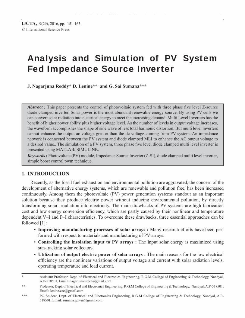
From fi gure (1.b) the relation between the output Vpv and the output current Ipv can be expressed as:
IPV = IL – ID = IL – Io
V I Rexp 1pv pv s –
é ùæ ö+ ÷çê ú÷ç ÷ê úç ÷çè øë û (1)
where IL = Light current; Io = Saturation current; Rs = Series Resistance; α = Thermal voltage timing completion factor. The above four parameters are need to be determined to obtain the I-V characteristics of PV-module. Thus, this model can be termed as Four-parameter model. The equations for determining the four parameters are given below.
The non-linear of Vpv – Ipv and P–Vpv curves are correspondingly drawn as shown below:
Fig. 2. Vpv – Ipv and P-Vpv characteristics of a PV cell.
(i) Light Current (IL)
IL = ref
GG
(ILref + μISC (TC – TCref )) (2)
Where G = solar irradiance (W/m2); Gref = reference irradiance, ILref = light current at the reference condition; TC = PV cell temperature (°C); TCref = reference cell temperature (25°C is used in this study); μIsc = temperature coeffi cient of the short-circuit current (A/°C).
(ii) Saturation Current (IO)
Io = 3
Cref CrefOref
C s ref C
T 273 T 273I exp 1T 273 N T 273
gape q–
æ öæ ö æ ö+ + ÷÷ ç ÷ç ç ÷÷ ÷çç ç ÷÷ ÷çç ç ÷÷ ÷ç ç ÷ç+ µ +è ø è øè ø (3)
Where Ioref = saturation current at the reference condition (A); egap = band gap of the material 1.17 eV for Si materials); Ns = number of cells in series of a PV module; q = charge of an electron (1.60217733×10⁻¹⁹ C); αref = the value of α at reference condition.
Ioref can be calculated as:
IOref = ILref exp OCref
ref
V–æ ö÷ç ÷ç ÷ç ÷ç µè ø
(4)
(iii) Calculation of α
= Cref
Cref
T 273T 273
+µ
+ (5)

154 J. Nagarjuna Reddy, D. Lenine and G. Sai Sumana
The value of αref can be calculated as:
ref = SC
SC S
2V VI I
1I I I
mpref ocref
ref mpref
ref mpref cref
–
ln ––
æ ö÷ç ÷ç+ ÷ç ÷÷çè ø
(6)
Where Vmpref = maximum power point voltage at the reference condition (V); Impref = maximum power point current at the reference condition (A); Iscref = short circuit current at the reference condition (A). From the above equation for α, it can be observed that α is a function temperature.
(iv) Series Resistance (RS)
Some manufacturers provide the value of Rs. If not provided, the following equation can be used to estimate its value:
RS = OCrefSCref
Iln 1 V V
II
mprefref mpref
mpref
– –æ ö÷ç ÷µ +ç ÷ç ÷çè ø (7)
RS is taken as a constant in the model of this study.
(v) Thermal Model of PV
From equations (1) to (6), it can be noted that the temperature plays an important role in the PV performance. Therefore, it is necessary to have a thermal model for a PV cell/module. In this study, a lumped thermal model is developed for the PV module. The temperature of the PV module varies with surrounding temperature, irradiance, and its output current and voltage, and can be written as:
CPV CTd
dt = PV PV
loss CV IK G K (T – T )
Ainpv a– – (8)
CPV = the overall heat capacity per unit area of the PV cell/ module[J/(C–m2)]; Kinpv = Transmittance-absorption product of PV cells ; Kloss = overall heat loss coeffi cient [W/(°C–m2)]; Ta = ambient temperature (°C); A = effective area of the PV cell/module (m2).
3. Z-SOURCE INVERTER
Fig. 3. Generation of Switching pulses to Conventional & ZSI.
155Analysis and Simulation of PV System Fed Impedance Source Inverter
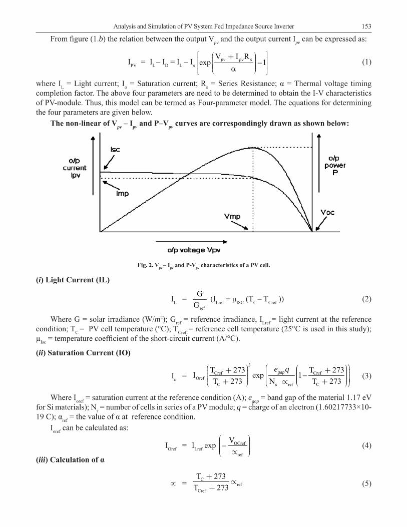
The Conventional Inverter will operate in two states: active state & null state. In ZSI along with active state & null State, the third state i.e., shoot through state is allowed. In six active states and in zero-state (null state) mode, the ZSI operates as conventional inverter. In the shoot-through state, all the switches in one or more legs are turned on. The operating states of conventional inverter & ZSI are shown in Fig. 3. Null states are represented as “0” & shoot through state is represented as “1”. From this fi gure It is observed that shoot through states are inserted in the null states without disturbing the active states. By controlling the shoot through duration the DC link voltage is varied, which in turn modifi es the output voltage magnitude to any desired value [5].
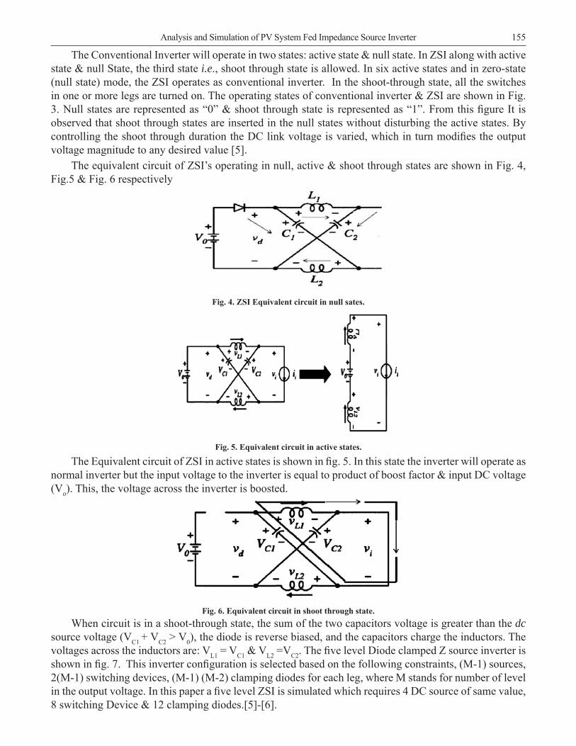
The equivalent circuit of ZSI’s operating in null, active & shoot through states are shown in Fig. 4, Fig.5 & Fig. 6 respectively
Fig. 4. ZSI Equivalent circuit in null sates.
Fig. 5. Equivalent circuit in active states.
The Equivalent circuit of ZSI in active states is shown in fi g. 5. In this state the inverter will operate as normal inverter but the input voltage to the inverter is equal to product of boost factor & input DC voltage (Vo). This, the voltage across the inverter is boosted.
Fig. 6. Equivalent circuit in shoot through state.When circuit is in a shoot-through state, the sum of the two capacitors voltage is greater than the dc
source voltage (VC1 + VC2 > V0), the diode is reverse biased, and the capacitors charge the inductors. The voltages across the inductors are: VL1 = VC1 & VL2 =VC2. The fi ve level Diode clamped Z source inverter is shown in fi g. 7. This inverter confi guration is selected based on the following constraints, (M-1) sources, 2(M-1) switching devices, (M-1) (M-2) clamping diodes for each leg, where M stands for number of level in the output voltage. In this paper a fi ve level ZSI is simulated which requires 4 DC source of same value, 8 switching Device & 12 clamping diodes.[5]-[6].

156 J. Nagarjuna Reddy, D. Lenine and G. Sai Sumana
To generate shoot through state one of the following switching combination is used. 1. To get complete shoot through state, the Switches Sa1, Sa2, Sa3, Sa4, Sa1
1, Sa21, Sa3
1 & Sa41 are turned
on. 2. To get shoot through state in Z source 1 alone, the switches Sa1, Sa2, Sa3, Sa4, Sa1
1 & Da4 are turned on.
3. To get shoot through period in Z source 2 alone, the switches Da1, Sa2, Sa3, Sa4, Sa11 Sa2
1 & Da5 are turned on
4. To get shoot through period in Z source 3 alone, the switches Da2, Sa3, Sa4, Sa11 Sa2
1 Sa31 & Da6 are
turned on 5. To introduce shoot through period in Z source 4 alone, the switches Da3, Sa4, Sa11, Sa21, Sa31 & Sa4
1 are turned on
6. To get upper shoot through state (ZSI1 & ZSI2), the switches Sa1, Sa2, Sa3 and Sa4 are turned on 7. To get lower shoot through state (ZSI3 & ZSI4), the switches Sa11, Sa2
1, Sa31 & Sa4
1 are turned onAlong with the above combination there exist other switching combinations to create shoot through
state.
Fig. 7. Z source based Multilevel Inverter.
4. PWM TECHNQIUES FOR ZSI (i) Simple Boost Method
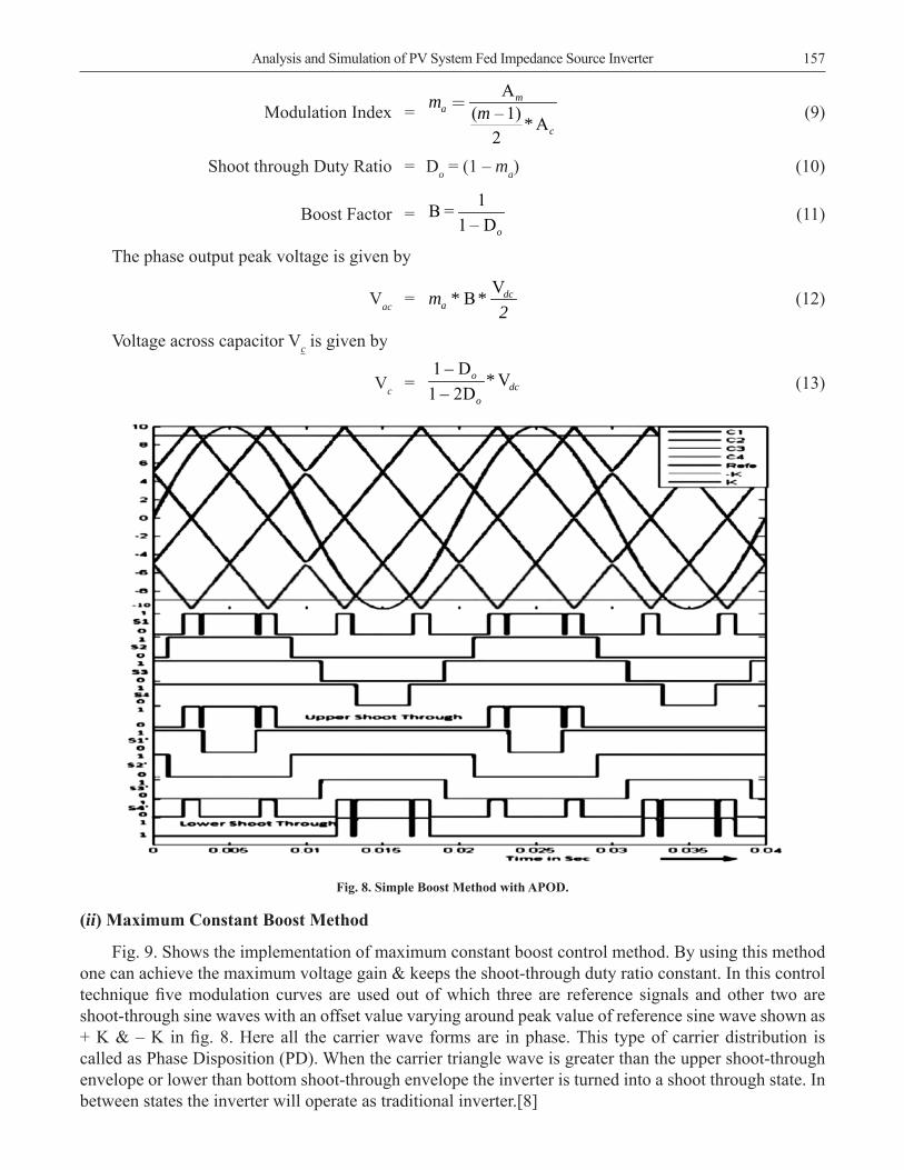
This method uses two straight lines of equal magnitude with opposite polarities are used shown in Figure 8. To insert shoot through state the magnitude of carrier wave must be greater than the carrier. In this method all carriers are in phase opposition with the neighbor carriers & it is called as Alternate Phase Opposition Disposition (APOD). When the carrier waveform is greater than the upper constant, or lower than the bottom constant line the circuit goes into shoot through state. Otherwise it operates as a conventional carrier based PWM. This method is very simple. However, the resulting voltage stress across the switches is relatively high because some traditional zero states are not utilized. The theoretical values of modulation index, shoot through duty ratio, boost factor, output peak ac voltage & voltage across capacitors is obtained by using below equations[7]-[11].
157Analysis and Simulation of PV System Fed Impedance Source Inverter
Modulation Index = A
( – 1) A2
ma
c
m m *= (9)
Shoot through Duty Ratio = Do = (1 – ma) (10)
Boost Factor = 1B =
1 – Do (11)
The phase output peak voltage is given by
Vac = VB dcam * *
2 (12)
Voltage across capacitor Vc is given by
Vc = 1 D V
1 2Do
dco
– *– (13)
Fig. 8. Simple Boost Method with APOD.
(ii) Maximum Constant Boost Method
Fig. 9. Shows the implementation of maximum constant boost control method. By using this method one can achieve the maximum voltage gain & keeps the shoot-through duty ratio constant. In this control technique fi ve modulation curves are used out of which three are reference signals and other two are shoot-through sine waves with an offset value varying around peak value of reference sine wave shown as + K & – K in fi g. 8. Here all the carrier wave forms are in phase. This type of carrier distribution is called as Phase Disposition (PD). When the carrier triangle wave is greater than the upper shoot-through envelope or lower than bottom shoot-through envelope the inverter is turned into a shoot through state. In between states the inverter will operate as traditional inverter.[8]

158 J. Nagarjuna Reddy, D. Lenine and G. Sai Sumana
Modulation Index = A
( – 1) Am
a
c
m m *2
= (14)
Shoot through Duty Ratio = 3D 1 a
o* m–2
æ ö÷ç ÷=ç ÷ç ÷÷çè ø (15)
Boost Factor = 1B
3 1am –= (16)
The phase output peak voltage is given by
Vac = VB2dc
am * * (17)
Voltage acroos capacitor Vc is given by
Vc = 1 D2 V1 – 2D3
odc
o
– * (18)
Fig. 9. Maximum constant Boost method with PD.
(iii) Maximum Boost Method
Fig. 10. Shows the implementation of maximum boost control strategy. In this control method, the six active states are unchanged and turns all zero states into shoot-through states. Thus maximum shoot through time interval, maximum Boost Factor and maximum voltage gain are obtained for any given modulation index M without distorting the output waveforms. It can be seen from Fig. 10 that, circuit is in shoot-through state when the carrier wave is either larger than the maximum value of the references or lesser than the minimum of the references. All carrier waveforms above the zero reference are in phase and are out of phase with those below zero reference by 180°. This type of carrier distribution is called as Phase Opposition Disposition (POD). [8]-[10].

159Analysis and Simulation of PV System Fed Impedance Source Inverter
Modulation Index = A
( – 1) Am
a
c
m m *2
= (19)
Shoot through Duty Ratio = 2 3 3D2
ao
– m
= (20)
Boost Factor = B3 3 am –
= (21)
The phase output peak voltage is given by
Vac = VB2dc
am * * (22)
Voltage acroos capacitor Vc is given by
Vc = 1 D2 V
1 2D2 3o
dco
–* *–
(23)
Fig. 10. Maximum Boost PWM technique with POD.
5. SIMULATION RESULTS
To study the performance of PV system fed Z source inverter, simulations were performed in MATLAB/SIMULINK.
(i) Model Performance of PV System
Based on the mathematical equations discussed before, a dynamic model for a PV module consisting of 153 cells in series has been developed using MATLAB/Simulink. The input quantities (solar irradiance G and the ambient temperature Ta) together with manufacturer data are used to calculate the four parameters. Then, based on equation (1), the output voltage is obtained numerically. The thermal model

160 J. Nagarjuna Reddy, D. Lenine and G. Sai Sumana
is used to estimate the PV cell temperature. The two output quantities (PV output voltage Vpv and the PV cell temperature Tc), and the load current Ipv, are fed back to participate in the calculations. The model parameters used in the simulation are given in Table I.[1]-[2]
Table 1. The PV Model Parameters.
ISCref(ILref) 2.664A Gref 1000w/m2
αref 5.472 Tcref 25°c
RS 1.324Ω Cpv 5*104J/(0c-m2)
VOCref 87.72V A 1.5m2
VMPref 70.731V Kinpv 0.9
IMPref 2.448A Kloss 30W/(0c-m2)
The model Ipv–Vpv characteristic curves under different irradiances are given in Figure 11 at 25˚C. It is noted from the fi gure that the higher is the irradiance, the larger are the short-circuit current (Isc) and the open-circuit voltage (Voc). And, obviously, the larger will be the maximum power (P), shown in Figure 12.
Fig. 11. Vpv–Ipv characteristics for constant Tc and Varying G.
Fig. 12. P–Vpv characteristics for constant Tc and Varying G.
161Analysis and Simulation of PV System Fed Impedance Source Inverter
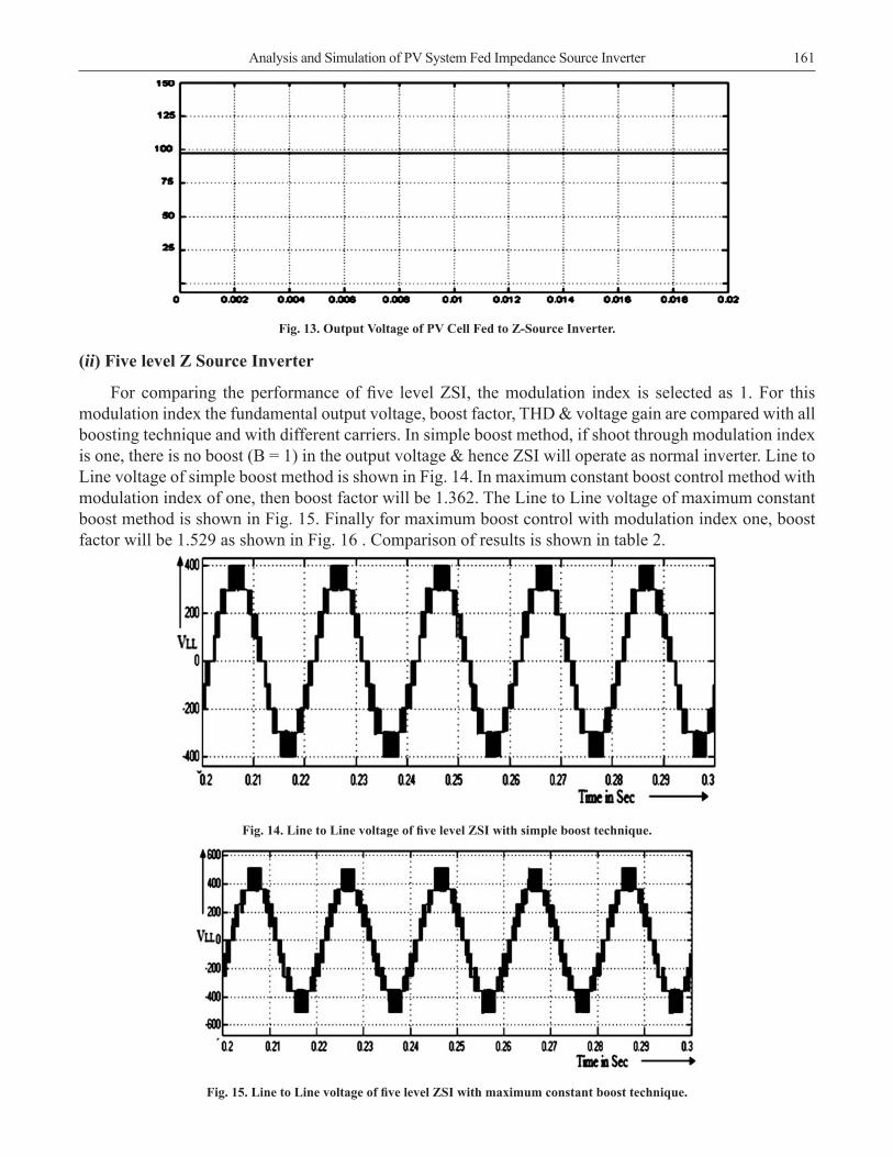
Fig. 13. Output Voltage of PV Cell Fed to Z-Source Inverter.
(ii) Five level Z Source Inverter
For comparing the performance of fi ve level ZSI, the modulation index is selected as 1. For this modulation index the fundamental output voltage, boost factor, THD & voltage gain are compared with all boosting technique and with different carriers. In simple boost method, if shoot through modulation index is one, there is no boost (B = 1) in the output voltage & hence ZSI will operate as normal inverter. Line to Line voltage of simple boost method is shown in Fig. 14. In maximum constant boost control method with modulation index of one, then boost factor will be 1.362. The Line to Line voltage of maximum constant boost method is shown in Fig. 15. Finally for maximum boost control with modulation index one, boost factor will be 1.529 as shown in Fig. 16 . Comparison of results is shown in table 2.
Fig. 14. Line to Line voltage of fi ve level ZSI with simple boost technique.
Fig. 15. Line to Line voltage of fi ve level ZSI with maximum constant boost technique.

162 J. Nagarjuna Reddy, D. Lenine and G. Sai Sumana
Fig. 16: Line to Line voltage of fi ve level ZSI with maximum boost technique
Table 2. Comparison Table For Five Level Z Source Inverters.
Boosting Type of Fundamental % of THD Voltage Stress across the Technique Carrier voltage switch in Volts Simple PD 347.7 15.51 100 Boost POD 344.7 19.2 100 APOD 344.3 21.48 100 Maximum PD 426.5 18.25 100 constant POD 430.4 24.17 102 Boost APOD 430.1 27.5 103 Maximum PD 597.8 19.28 107 Boost POD 566.4 22.03 105 APOD 569.9 29.93 110
From comparison Table 2 it is clear that system is giving better performance with Phase disposition carrier when compared to phase opposition disposition & Alternate Phase opposition disposition carrier.
6. CONCLUSION
This paper investigates the voltage gain, THD and voltage stress with three major types of boosting techniques used for ZSI when connected to PV system using MATLAB/SIMULINK. Based on the availability of input & requirement of load, proper control method is chosen. THD is controlled by increasing the number of levels in the output voltage. Simple boost method is easy for the implementation but available output voltage is limited and voltage stress across the switches increases. Maximum boost method will have good voltage gain and voltage stress across the switches is reduced when compare to simple & maximum constant boost method.
7. REFERENCES 1. Reddy, J. Nagarjuna, B. M. Manjunatha, and Mallikarjuna Matam. “Improving effi ciency of Photovoltaic System
with Neural Network Based MPPT Connected To DC Shunt Motor.” International Journal of Modern Engineering Research 3.5 (2013): 901-2907.
2. Cashing Wang “Modeling and Control of Hybrid Wind/Fuel Cell/Distributed Systems”, Ph.D Thesis, Montana State University, Bozeman, Montana, July 2006.

163Analysis and Simulation of PV System Fed Impedance Source Inverter
3. Manjunatha, B. “Advanced Pulse Width Modulation Techniques for Z Source Multi Level Inverter”. World Academy of Science, Engineering and Technology, International Science Index 99, International Journal of Electrical, Comput-er, Energetic, Electronic and Communication Engineering, (2015), 9(3), 359 - 364.
4. J. H. Park “A Control Strategy for the Grid-connected PV System Using a Z-Source Inverter,” 2nd IEEE Internation-al Conference on Power and Energy (PECon 08), December 1-3, 2008, Johor Baharu, Malaysia
5. F. Z. Peng, “Z source Inverter,” IEEE Trans. Ind. Appl., vol. 39, pp. 504-510, March/April 2003
6. S. Thangaprakash, A. Krishnan, “Comparative evaluation of modifi ed pulse width modulation schemes of Z-source inverter for various applications & demands,” International journal of Engineering, Science and Technology, Vol. 2, No. 1, 2010, pp. 103-115
7. K. Janardhana, P. Agarwal “Performance Analysis of Different PWM control for Three-Phase Z-Source Inverter,” UACEE international journal of advancement in Electronics and Electrical engineering vol. 1, No. 1.
8. P. C. Loh, F. Blaabjerg, and C. P. Wong, “Comparative evaluation of pulse width modulation strategies for Z-source neutral-point-clamped inverter,” IEEE Trans. Power Electron., vol. 22, no. 3, pp. 1005-1013, May 2007
9. P. C. Loh, F. Gao, F. Blaabjerg, S. Y. Feng, and K. N. Soon, “Pulse Width Modulated Z-source neutral-point-clamped inverter,” IEEE Trans. Ind. Appl., vol. 43, no. 5, pp. 1295-1308, Sep./Oct. 2007.
10. Miaosen Shen and Peng.F.Z, “Operation Modes and Characteristics of the Z-source Inverter with small inductance”, IEEE Trans. Ind. Appl., Vol. 55, No.1, pp. 89-96, Jan., 2008.
11. P. C. Loh, S. W. Lim, F. Gao, and F. Blaabjerg, “Three-level Z-source Inverters using a single LC impedance net-work,” IEEE Trans. Power Electron., vol. 22, no. 2, pp. 706-711, Mar. 2007


![CPW-Fed Slot Antenna for Wideband Applicationsdownloads.hindawi.com/journals/ijap/2008/379247.pdfslot antenna with linear taper is presented in [12] to increase the impedance bandwidth](https://img.dokumen.tips/doc/110x75/5eb2153555a03648d618ab54/cpw-fed-slot-antenna-for-wideband-a-slot-antenna-with-linear-taper-is-presented.jpg)