Embed Size (px)
Citation preview
Nuclear Inst. and Methods in Physics Research, A 959 (2020) 163479
Contents lists available at ScienceDirect
Nuclear Inst. and Methods in Physics Research, A
journal homepage: www.elsevier.com/locate/nima
Analysis and numerical design of Resistive AC-Coupled Silicon Detectors(RSD) for 4D particle trackingM. Mandurrino a,∗, R. Arcidiacono a,b, M. Boscardin c,d, N. Cartiglia a, G.-F. Dalla Betta d,e,M. Ferrero a,f, F. Ficorella c,d, L. Pancheri d,e, G. Paternoster c,d, F. Siviero a,f, V. Sola a,f, A. Staiano a,A. Vignati a
a INFN, Sezione di Torino, Via P. Giuria, 1, 10125 Torino, Italyb Universitá del Piemonte Orientale, Largo Donegani, 2/3, 20100 Novara, Italyc Fondazione Bruno Kessler, Via Sommarive, 18, 38123 Povo (TN), Italyd TIFPA-INFN, Via Sommarive, 18, 38123, Povo (TN), Italye Universitá degli Studi di Trento, Via Sommarive, 9, 38123 Povo (TN), Italyf Universitá degli Studi di Torino, Via P. Giuria, 1, 10125 Torino, Italy
A R T I C L E I N F O
Keywords:TCAD modelingCharge multiplicationSolid-state silicon detectorsParticle tracking detectorsParticle timing detectorsFast detectors
A B S T R A C T
In this paper we present the numerical simulation of silicon detectors with internal gain as the main tool for 4-dimensional (4D) particle trackers design and optimization. The Low-Gain Avalanche Diode (LGAD) technologyand its present limitations are reviewed with the aim of introducing the Resistive AC-Coupled Silicon Detectors(RSD) paradigm as a case study of our investigation. Authors here present Spice-like and 2D/3D TechnologicalComputer-Aided Design (TCAD) simulations to characterize sensors in terms of both their electrostatic behavior,capacitive (dynamic) coupling and radiation-hardness performances, showing the methodological approachused in order to extract the set of layout rules allowing the release of RSD1, the incoming production runat Fondazione Bruno Kessler (FBK) of next-generation silicon detectors for 4D tracking with intrinsic 100%fill-factor.
1. Introduction
Numerical simulation is an effective tools to design new detectorstructures and optimize existing devices. The technique described inthis work is based on the well-known Technology Computer-AidedDesign (TCAD) approach. By solving the Drift-Diffusion model forthe structures under consideration through the commercial softwareSentaurus Device by Synopsys, we are able to predict the generalbehavior of our devices as well as all the critical features characterizingtheir operation. Such procedure allowed to define the layout rulesleading us to submit the lithographic masks of a first batch of ResistiveAC-Coupled Silicon Detectors (RSD), produced by Fondazione BrunoKessler (FBK) in Trento, Italy.
2. The role of RSD in 4D particle tracking
One of the most difficult challenges in silicon technology for 4Dparticle tracking is to combine the spatial and timing information whilemaintaining high levels of accuracy in both aspects. To this purpose,in the past years, the Italian National Institute for Nuclear Physics(INFN) in Torino developed the Ultra-Fast Silicon Detectors (UFSD), a
∗ Corresponding author.E-mail address: [email protected] (M. Mandurrino).
project aiming at improving the measurement of particle arrival timethrough the LGAD paradigm [1,2]. Essentially, LGAD are 𝑛-in-𝑝 sensorsensuring fast and large signals thanks to a proper p+-type gain layerimplanted beneath the cathode. In reverse polarization regime, suchlayer is responsible for the multiplication of primary charges that areproduced by traveling particles through the impact ionization of latticeatoms. By keeping the multiplication factor, or gain 𝐺, adequately low,it has been demonstrated that it is possible to have large output signalamplitude with, at the same time, a noise below the electronics readoutnoise [3].
For their timing performance, LGAD sensors have now been chosenfor the upgrade of CMS and ATLAS experiments at CERN in viewof High-Luminosity LHC (HL-LHC) [4]. In fact, with the expectedluminosity in excess of about 1035 cm−2s−1, between 10%–20% ofvertices identified by the inner tracking detector will be composed bythe overlap of two subsequent pp collisions that happen so close to eachother in space to be mistakenly interpreted as a single interaction. Theonly way to correctly disentangle such vertices is to measure the time ofeach track: as the interactions of each bunch crossing occur randomlyin a time spread of the order of 150 ps, measuring the time of each track
https://doi.org/10.1016/j.nima.2020.163479Received 29 April 2019; Received in revised form 13 January 2020; Accepted 19 January 2020Available online 22 January 20200168-9002/© 2020 Elsevier B.V. All rights reserved.
M. Mandurrino, R. Arcidiacono, M. Boscardin et al. Nuclear Inst. and Methods in Physics Research, A 959 (2020) 163479
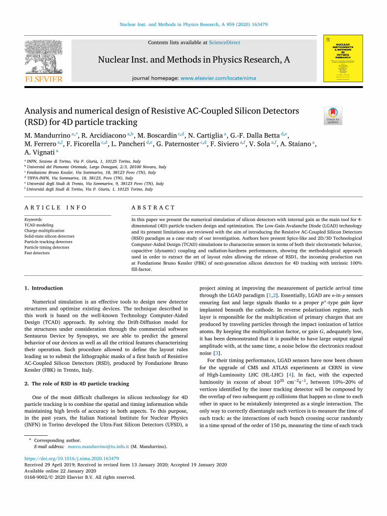
Fig. 1. (a) Cross section of the segmentation structures between two adjacent LGADactive areas and (b) gain 𝐺 as a function of the particle hit position calculated throughnumerical simulations. In the dashed rectangle: simple-2D slice including only theessential LGAD implants to be used in simplified simulations.
with an accuracy of about 30–35 ps can remarkably reduce the overlap,allowing current reconstruction algorithms to distinguish almost alwaysthe two collisions.
To obtain also a good spatial granularity with fast signals, one ofthe most used solutions is to implement LGAD sensors with patternedsensitive areas, where each pixel unit is identified by its gain implant.An important implication of such segmentation scheme is the needto avoid early breakdown at pixel edges and short-circuit betweennearby pixels. This is achieved through the implantation of propertermination structures between sensitive areas which are, respectively,the JTE and p-stop implants depicted in Fig. 1(a). This set of features,which compose the inter-pixel segmentation, determines a dead area(or no-gain area) for particle detection, having charge multiplicationonly when the particle passes through a gain area and not in the inter-pixel regions. To this purpose, it is useful to introduce the conceptof fill-factor, which is defined as the ratio between the gain area andthe total area. Panel (a) of Fig. 1 shows the segmentation structuresbetween two adjacent pixels of an LGAD sensor along with, in panel (b),the gain behavior as a function of the longitudinal position where thecharged particle hits the sensor. Due to hermetic coverage required byhigh-luminosity experiments – e.g., fill-factor must be > 95% in the CMSMIP Timing Layer (see, for instance, Refs. [4,5]) – the need of newtechnologies arises since, even though the smallest possible layout rulesare implemented, the dead area cannot be made smaller than ∼40 μm.This dimension results from the combination of two effects: (i) thephysical distance between gain implants, also inclusive of their lateralspreading distributions, and (ii) the effective gain turn-on, determinedby the shape of field lines in silicon.
To get rid of any gain loss due to segmentation structures, we de-signed Resistive AC-Coupled Silicon Detectors (RSD), which essentiallyare LGAD optimized for both spatial and timing detection (4D-tracking)with high segmentation level [6]. They are currently being developed inTorino under a contract framework between INFN and FBK. Benefitingfrom the experience gained in the LGAD framework in terms of radia-tion hardness and time resolution, their process flow is almost as simpleas that of the LGAD. This translates into low-budget production costsand large areas implementation. The RSD operation principle is basedon the resistive AC-coupled readout, as shown in panel (a) of Fig. 2,where the detector bulk is modeled by a grid of capacitors 𝐶det con-nected to a resistive 𝑛+ layer of a given sheet resistance 𝑅sheet (∼k𝛺).The readout takes place via AC-coupling capacitors 𝐶AC, designed toinduce a signal on the metal pads. In this layout the resistive electrodeis required to be such that the multiplied charges are kept frozen for acharacteristic time sufficient to guarantee the complete signal inductionbefore being discharged, but also short enough to minimize pile-up
effects. Then the discharge occurs through proper DC contacts (notrepresented in Fig. 2) that are usually located at the device periphery,on the front side.
Having such readout scheme, with signals that are locally inducedon the pad where charges have been generated, RSD do not requirethe segmentation layout proper of standard technology. For this reasonthey can be realized with both continuous gain layer and 𝑛-electrodeimplants, allowing spatial reconstruction of tracks with a fill-factorintrinsically equal to 100%. A drawback of the RSD technology mightbe represented by the charge sharing between adjacent pads, that canbe kept under control by an accurate engineering of the doping profileworking as cathode layer and, in turn, of its effective sheet resistance.Panels (b) and (c) of Fig. 2 show, respectively, the cut of an RSD device(notice the continuity of the 𝑝+ gain layer) and its simplified circuitalmodel for a single node of the electrical grid. As one may note, theresistive stage is implemented through an optimized version of theusual 𝑛 layer, while the AC-coupling is realized by placing a capacitivedielectric spacer between silicon and readout electrodes. In this newparadigm, both the cathode and the gain layer remain homogeneousand constant along the sensor area, creating an almost uniform electricfield. It is a key element of the design that, even though the volumeof the whole sensor might be rather large, each AC readout pad, dueto the resistive sheet, is sensitive only to a small region of the detector(or, in other words, to the local value of 𝐶det), and it will be almostuncorrelated to the total leakage.
3. Modeling methods and simulation
In order to calculate the signal generated by the RSD under ir-radiation, 1D preliminary TCAD simulations using the drift-diffusion(DD) framework have been used (see [7,8] as previous referencesfor numerical simulation of charge multiplication in silicon particledetectors). Then, the output waveforms are implemented into Spiceto simulate the electrical behavior of a full sensor module and extractthe most important design parameters, i.e. the electrode resistivity, theoxide thickness with its capacitance and the pad size and pitch. Afterthis calibration, 2D and 3D simulations have been performed with aTCAD tool in order to characterize the RSD devices in terms of chargemultiplication, static/dynamic electrical properties (such as 𝐶(𝑉 ), 𝐼(𝑉 ),charge sharing or signal capacitive coupling), radiation resistance and,consequently, to define all the layout rules for the first production runof sensors.
3.1. The drift-diffusion framework
For the purposes explained in the introduction, we have chosen touse a commercial tool [9] based on the drift-diffusion (DD) model,where the Poisson equation of semiconductors
∇2𝐫 𝜑(𝐫, 𝑡) = −
𝜌(𝐫, 𝑡)𝜖
, (1)
describing the coupling between the electric field = −∇𝐫 𝜑 and thetotal charge density 𝜌 = 𝑞 (𝑝 − 𝑛 + 𝐶), is self-consistently solved withthe continuity equations for electrons and holes𝜕𝑛(𝐫, 𝑡)
𝜕𝑡= + 1
𝑞∇𝐫 𝐽𝑛(𝐫, 𝑡) − 𝑈𝑛(𝐫, 𝑡)
𝜕𝑝(𝐫, 𝑡)𝜕𝑡
= − 1𝑞∇𝐫 𝐽𝑝(𝐫, 𝑡) − 𝑈𝑝(𝐫, 𝑡)
(2)
where 𝜑 is the electrostatic potential, 𝜖 the isotropic dielectric con-stant, 𝑞 is the elementary charge, 𝑝, 𝑛 and 𝐶 are, respectively, thedensity of holes, electrons and fixed charges (like defects and traps),𝐽𝑛,𝑝 is the electron/hole current density and 𝑈𝑛,𝑝 the net genera-tion/recombination (GR) rate of charge carriers, i.e. the number ofelectron/hole pairs generated or recombined per cm3 in the unit time.Within the DD framework
𝑈 (𝐫, 𝑡) = 𝐺(𝐫, 𝑡) − 𝑅(𝐫, 𝑡) , (3)
2

M. Mandurrino, R. Arcidiacono, M. Boscardin et al. Nuclear Inst. and Methods in Physics Research, A 959 (2020) 163479
Fig. 2. Basic operational principles of the resistive AC-coupled readout: (a) Electronic equivalent circuit. (b) Cross-sectional sketch of a silicon n-in-p RSD where the 𝑛-type cathode,freezing the charges, and a cap dielectric, to allow the signal transfer to the pads by capacitive induction, are represented. (c) Circuital model in correspondence of a single nodeof the resistive sheet, i.e. for a readout pad.
where 𝐺 and 𝑅 terms respectively represent the generation and re-combination rates, and all current densities are computed as a sumof a drift contribution, driven by the electric field, and a diffusioncomponent, determined by the gradient of charge concentration so that,for electrons,
𝐽𝑛(𝐫, 𝑡) = 𝐽diff𝑛 (𝐫, 𝑡) + 𝐽drift
𝑛 (𝐫, 𝑡)
= 𝑞[
𝐷𝑛∇𝐫 𝑛(𝐫, 𝑡) − 𝜇𝑛(
∇𝐫 𝜑(𝐫, 𝑡))
𝑛(𝐫, 𝑡)]
(4)
and similarly for holes, where
𝐷𝑛,𝑝(𝐫, 𝑡) = 𝜇𝑛,𝑝(𝐫, 𝑡)𝑘B𝑇𝑞
(5)
are the Einstein diffusion coefficients for electrons and holes, 𝜇𝑛,𝑝 theirmobilities, written as
𝜇𝑛,𝑝(𝐫, 𝑡) =𝑣drift𝑛,𝑝
(𝐫, 𝑡)= −
𝑣drift𝑛,𝑝
∇𝐫 𝜑(𝐫, 𝑡), (6)
and 𝑣drift𝑛,𝑝 are the electron/hole drift velocities due to the local internal
field .To solve the set of partial differential equations (PDE) composing
the DD model written in Eqs. (1)–(2), we have to adopt a scheme forsampling all the physical quantities to be computed inside the detectorof our interest and linearize the system. To this purpose the devicegeometry is discretized with the Scharfetter–Gummel triangulation pro-cedure and, by applying proper boundary conditions (BC), the DDsystem is linearized through a finite boxes (FB) approach and then issolved with the Newton iterative method at each node of the discretiza-tion grid. The GR mechanisms accounted for as proper net rates 𝑈are the Shockley–Read–Hall (SRH), band-to-band tunneling (BTBT) andavalanche impact ionization. In particular, charge multiplication hasbeen implemented by means of three commonly used models: Massey,van Overstraeten–de Man and Okuto-Crowell model (see Refs. [10–12]). They are all describing the avalanche charge multiplication insilicon as
𝑈aval = 𝛼𝑛𝑛𝑣𝑛 + 𝛼𝑝𝑝𝑣𝑝 , (7)
where 𝑈aval is the net GR rate for the avalanche ionization, 𝑣𝑛,𝑝 are thetotal carrier velocities and 𝛼𝑛,𝑝 represent the electron/hole ionizationcoefficients (in cm−1), whose expression, following the well-knownChynoweth law [13], varies according to the specific formalism weare taking into account. In particular, for the Massey model – thatwe implemented as an external C++ routine via the Sentaurus PMI(Physical Model Interface) tool, being not included among the built-infunctions – we have
𝛼Mas𝑛,𝑝 () = 𝐴Mas
𝑛,𝑝 exp
(
−𝐵Mas𝑛,𝑝 (𝑇 )
)
, (8)
while, in the van Overstraeten–de Man approach
𝛼vOv𝑛,𝑝 () = 𝛾 𝐴vOv
𝑛,𝑝 exp
(
−𝛾𝐵vOv𝑛,𝑝
)
(9)
and, finally, the Okuto–Crowell formalism reads
𝛼Oku𝑛,𝑝 () =𝐴Oku
𝑛,𝑝
(
1 + (𝑇 − 300)𝐶Oku𝑛,𝑝
)
× exp
⎡
⎢
⎢
⎢
⎣
−
⎛
⎜
⎜
⎜
⎝
𝐵Oku𝑛,𝑝
(
1 + (𝑇 − 300)𝐷Oku𝑛,𝑝
)
⎞
⎟
⎟
⎟
⎠
2⎤
⎥
⎥
⎥
⎦
, (10)
where the pre-factor 𝐴 (in cm−1), the critical field 𝐵 (V/cm), thecoefficient 𝛾, 𝐶 and 𝐷 (both in K−1) are different in the three models(see the Appendix or Ref. [7]).
By imposing proper initial conditions (IC) at the device electrodesand an initial guess for the electrostatic potential 𝜑, the TCAD solvercan self-consistently evaluate all the nodal unknowns, such as theelectron/hole carrier and current densities (𝑛, 𝑝 and 𝐽𝑛,𝑝), as well asthe device-level macroscopic output quantities (total current flowingthrough the detector, capacitance or induced signals).
3.2. Radiation damage modeling
Being the RSD technology conceived to operate also in radiation-intense frameworks, its TCAD-based design and optimization has tonecessarily include the role of lattice damaging mechanisms. The ev-idence of trap states production in silicon under irradiation has beenextensively reported in literature since 50s of the last century (see, forinstance, Ref. [14]), and it can be simply managed from the numericalviewpoint by introducing proper ad-hoc empirical laws for each familyof defects where the overall trap density is modeled through a certainfunction of the radiation fluence 𝜙 (in cm−2).
But the phenomena which we are more interested in are somecrystal-level modifications occurring to dopant atoms in correspon-dence of the multiplication implant and, in particular, the mechanismsknown in the literature as acceptor deactivation (sometimes also goingunder the less proper name of acceptor removal). Indeed, more recentobservations [15] reported that the active (substitutionals) acceptorelements are removed from their lattice sites due to a two-step process:(i) the radiation produces interstitial Si atoms that subsequently (ii) cap-ture and deactivate the doping elements via kick-out reactions (Watkinsmechanism [16]) producing ion-acceptor complexes (interstitials) [17].
The strategy we used to introduce both the defect production anddeactivation mechanisms in our simulations consists in an off-linerecomputation of the gain layer and acceptor bulk profiles accordingto the model [2]
𝑁A(𝜙, 𝑥) = 𝑔eff 𝜙 +𝑁A(0, 𝑥) e−𝜙 𝑐(𝑁A(0,𝑥)) . (11)
Here the resulting acceptor concentration, function of both the fluence𝜙 and the initial (nominal) acceptor density 𝑁A(0, 𝑥), is the linearcombination of a term accounting for the effective generation of traps,𝑔eff 𝜙, and an exponential contribution coming from the acceptor deac-tivation occurring within the p+-type gain layer. In the case of LGAD
3

M. Mandurrino, R. Arcidiacono, M. Boscardin et al. Nuclear Inst. and Methods in Physics Research, A 959 (2020) 163479
technology, it has been empirically proven that 𝑔eff ≃ 0.02 cm−1
provides a good description of the first mechanism [18,19].In Eq. (11), the acceptor deactivation coefficient 𝑐
(
𝑁A(0, 𝑥))
(incm2) is the inverse of the fluence needed to reduce the initial dopingdensity 𝑁A(0, 𝑥) by a factor 1∕e, and has been empirically modeled by(see details in Ref. [19])
𝑐(
𝑁A(0, 𝑥))
= 𝑘c𝑁Si ⋅𝑁int ⋅ 𝜎Si0.63 ⋅𝑁A(0, 𝑥)
1
1 +( 𝑁A,crit𝑁A(0,𝑥)
)23
, (12)
where 𝑘c is the probability of capturing a doping element, 𝜎Si (in cm−2)the Silicon cross-section of the scattering process with the ionizingparticle, 𝑁Si (5 ⋅1022 cm−3) and 𝑁int (in cm−3) are, respectively, the Sil-icon atomic density in the lattice and the concentration of interstitialscreated by radiation and, finally, where 𝑁A,crit (in cm−3) is an empiricalfitting parameter indicating the critical acceptor concentration at whichthe interstitial Silicon atoms have a probability of 0.5 to capture anddeactivate an acceptor state.
From such model the fact that the acceptor density profile hasto be corrected locally (in space 𝑥) comes quite straightforwardly.Furthermore, it has to be noticed that parameters 𝑁int, 𝜎Si and 𝑁A,critmay assume different values depending on whether we irradiate silicondetectors samples with protons or neutrons, while the value of 𝑘c ismainly subjected to the chemical nature of acceptor dopants used inthe gain layer (e.g., Boron or Gallium) and for the bulk doping.
3.3. Calibration of the minimum ionizing particle (MIP) energy release
In reverse bias and full-depletion conditions, and with electronsand holes at their saturation velocity, primary charges generated byan ionizing particle drift towards their respective electrodes: electronsto the 𝑛-cathode and holes to the 𝑝-anode. When such electrons driftacross the gain layer, they experience the high electric field responsiblefor the multiplication mechanism and participate to the phenomenonof avalanche impact ionization. For each primary electron a certainnumber of secondary (multiplied) electron/hole pairs are generatedthrough the further ionization of silicon atoms. This number is afunction of the electron velocity which, in turn, directly depends onthe electric field and, finally, on the applied reverse bias. This is thereason why, near a threshold field (∼300 kV/cm), there is the onsetof an exponential-like trend of the detector gain 𝐺 as a function theincreasing bias.
In order to study the charge multiplication after the passage of acharged particle, we activated in Sentaurus the Heavy Ion function,which emulates an ion traveling through the detector. This functionallows the user to control the amount of ionization energy releasedby the ion, that we want to set as the Minimum Ionizing Particle(MIP) energy. Typically, a MIP provides an energy large enough toproduce approximately 75 electron/hole pairs every micron of siliconcrossed. To correctly calibrate such number, we proceeded to test ourmodeling framework by comparing simulated and measured collectedcharges in silicon detectors coming from different vendors. In a firstphase, such calibration has been performed with p-i-n diodes, i.e. de-tectors without the internal multiplication layer, where the gain is onlydue to avalanche processes in the bulk under very-high electric fieldconditions.
By simulating the transient through which an heavy ion transfersits energy to the silicon lattice, the DD model is able to predict thenumber of electron/hole pairs generated at a given external voltageand then multiplied in the gain layer. Indeed, once one of the discussedavalanche models has been selected, its related net GR rate 𝑈aval writ-ten in Eq. (7) can be evaluated. Then, the avalanche impact ionizationcontribution to the total current density is computed at run-time inall the mesh nodes by self-consistently solving the electron/hole con-tinuity equations. The generated and multiplied charges are collectedby electrodes and give origin to a current pulse which is the result
of: (i) an induced current component 𝑖ind(𝑡) due to the charge carriersflowing underneath the electrode itself, as stated by the Shockley–Ramotheorem [20,21]
𝑖ind𝑛,𝑝 (𝑡) = 𝑞 𝑤 𝑣drift
𝑛,𝑝 , (13)
where 𝑤 is the so-called weighting field, and (ii) the current contribu-tion 𝑖col(𝑡) due to the carriers physically collected by the same electrode.Integrating in time the total current pulse 𝑖𝑛,𝑝(𝑡) = 𝑖ind
𝑛,𝑝 (𝑡) + 𝑖col𝑛,𝑝 (𝑡) we
can compute the amount of multiplied charge and, then, the detectorgain at a given bias. Notice that, in RSD, physical collection of chargeat readout electrodes does not take place anymore, since the signalsare exclusively due to a capacitive coupling induced by the dielectricseparation layer (see Fig. 2). The discharge will only occur throughproper DC contacts representing the grounded path for electrons.
Fig. 3 shows the comparison between simulated and measuredcollected charge as a function of the reverse applied voltage for 1 MIPin two irradiated p-i-n diodes coming from different foundries: CentroNacional de Microelectrónica (CNM), in Barcelona, and HamamatsuPhotonics K.K. (HPK), Japan [22]. In the following we will refer quiteindifferently to collected charge as to 𝐺(𝑉 ) characteristics, since thegain 𝐺 of an LGAD is obtained dividing the charge multiplied in thedetector with internal gain by the charge collected in the correspondingdevice without the multiplication layer. In p-i-n diodes, instead, the𝐺(𝑉 ) curve can be simply constructed by dividing the number ofcharges read at the electrode at a given bias by the charges collectedin low-injection regime (where there is no avalanche, and 𝐺 = 1).
The good agreement between simulations and measurements shownin Fig. 3 has been obtained by setting an ionizing energy transferequal to 56 and 70 pairs per micron, respectively, and by using allthe three avalanche formalisms to model the ionization coefficients𝛼𝑛,𝑝. Moreover, in order to take into account the effects of radiation insilicon, the trap generation law 𝑁A(𝜙) = 𝑔eff 𝜙 has been implemented.The difference we observe about the number of generated pairs in thesamples under investigation from the typical value of 75 electron/holepairs may be due to the uncertainty on the true active thickness, orcan be the effect of local discrepancies or fluctuations around thenominal value of 50 μm. Nevertheless, such difference simply reflectsthe necessity to calibrate our numerical setup, and gives an indicationof the modeling limitations. Moreover, as one may appreciate, Masseyand van Overstraeten–de Man models reproduce the measured chargewith a better accuracy.
As already said, being without any gain implant, p-i-n diodes havea multiplication onset occurring at relatively high applied bias. Thisoccurs because the only contribution to the avalanche mechanismcomes from the bulk, thus the electric field has to be raised along thewhole device depth, which means a high potential difference beforeexceeding the threshold field. So our procedure is useful to set the𝐺(𝑉 ) baseline in low-bias conditions (i.e. the number of depositedprimary charges) when the multiplication factor is unitary rather thanfor describing its exponential growth. At any rate, Fig. 3 demonstratesthat – at least in this temperature range and for the devices of ouranalysis – the Massey model reproduces quite well the measured 𝐺(𝑉 )trend also in the high-injection regime.
In order to have an even more robust numerical setup, the samecalibration has been performed by simulating the diode under thestimulus of a laser beam. This procedure allows us to compare thecalculated 𝐺(𝑉 ) curves also with experimental data where the chargeionization is provided through the IR light and not by ion irradiation as,for instance, in Transient Current Technique (TCT) measurements [24].We found that an optimum agreement can be found between 𝐺(𝑉 )curves simulated with heavy ions producing 56 pairs per micron andwith an IR laser (𝜆 = 1060 nm) releasing the energy density of 310W/cm2. The most important difference between using the IR laseror the heavy ion is that, if necessary, in the first case the softwareallows to use an illumination window with a finite width. This allowsto implement a certain intensity profile, very useful when comparingsimulations and TCT measurements, as mentioned before. Nevertheless,once the MIP has been calibrated in the experimental setup, there is nodifference between signals generated with a laser or with particles.
4

M. Mandurrino, R. Arcidiacono, M. Boscardin et al. Nuclear Inst. and Methods in Physics Research, A 959 (2020) 163479
Fig. 3. Measured (symbols) and simulated (lines) collected charge (or gain) for 1 MIP in 50 μm-thick devices: (a) p-i-n diode irradiated with neutrons at 𝜙 = 3 ⋅ 1015 neq/cm2 and(b) pions at 𝜙 = 1.5 ⋅ 1015 neq/cm2, respectively. Experimental data presented in Refs. [7,22,23].
3.4. Simple-2D TCAD simulations of avalanche diodes
Once we calibrated our numerical setup on the simple p-i-n diodes,we can solve the DD diffusion model for an LGAD in order to find theavalanche model that better reproduces the gain in the devices underconsideration. By implementing a simplified quasi-2D geometry whichincludes only the most important implants without any transversaldependence, as indicated by the dashed box in Fig. 1(a), we can predictsome important detector characteristics, such as 𝐼(𝑉 ; 𝑇 ) and 𝐺(𝑉 ; 𝑇 ),before or after irradiation, and below the Geiger operation mode (i.e. inthe moderate-gain regime). As an example, Fig. 4 shows the measuredand calculated gain for an unirradiated 50 μm-thick LGAD sample byHPK as a function of the applied bias as well as the temperature. Thethree avalanche models have been applied after emulating a laser beamwith energy density deposited of 310 W/cm2, while the gain has beencomputed by simulating both the device with the multiplication layerand its related p-i-n diode and then by dividing, for each bias point, thenumber of charges collected in the LGAD by the charges produced inthe version without gain of such device.
Again, as in the previous simulations, Massey model provides thebest-fitting agreement with the available experimental data, at least forthe bias and temperature range at our disposal.
To test the effectiveness of the radiation damage model presentedin the previous sections we proceeded by comparing our simulationswith gain measurements coming from irradiated detectors. Panel (a)of Fig. 5 shows both simulated and experimental collected charges inan LGAD sensor by FBK at different fluences, from the non-irradiationcondition to 𝜙 = 5 ⋅ 1014 neq/cm2. Even if also temperature is changingamong samples, the van Overstraeten–de Man model is able to predictquite well all the curves of charge versus applied bias. All the calculatedcharges are simulated through the laser beam approach, with a releasedenergy density of 310 W/cm2.
Moreover, in panel (b), one can find the trend of the bias requiredto collect 20k electrons as a function of the fluence for differentLGAD sensors produced by CNM and HPK. Here simulations have beenobtained by using the Heavy Ion function, generating 56 pairs permicron.
The plots included in Fig. 5 reflect the robustness of the empiricalradiation damage parametrization written in Eq. (11) in describing thecharge multiplication mechanism for irradiated LGAD-based particledetectors. Nevertheless, another important aspect is the precision levelin catching by numerical simulation the onset bias of the multipli-cation process as a function of the gain dopant dose and species,which represents an essential feature in developing new detectors.Before implementing the usual static simulations in order to studythe collected charge at different bias voltages, we tested the gainprofiles by comparing simulated and measured 𝐶(𝑉 ) characteristics
(both performed with 1 kHz AC signals) for different samples comingfrom the run UFSD2 [27], a second production of 50 μm-thick LGADdetectors designed at Trento University and produced by FBK in 2017.In panel (a) of Fig. 6, the measured capacitance characteristics havebeen used to extract the acceptor profiles (regarding this proceduresee, for instance, Ref. [19]) that have been included in the solver asinput data of our simulated 𝐶(𝑉 ). This important cross-check strategyrepresents a robust proof about the reliability of our numerical setup,being the agreement between experimental data and simulations highlysatisfactory. In particular, both the kink at low bias and the subsequentfoot before the baseline (corresponding respectively to the depletion ofgain layer and active volume) are perfectly modeled by TCAD.
Having verified that the solving architecture works properly, weused the same setup to simulate the 𝐺(𝑉 ) characteristics of four unir-radiated UFSD2 samples differing for the gain layer dopants: Gallium,Gallium with Carbon co-implantation, Boron and Boron with Carbonco-implantation. Both the Gallium and Carbon implants represent twoR&D solutions to mitigate the radiation damage in Silicon and, in par-ticular, the effects of acceptor deactivation mechanism [19]. Panel (b)of Fig. 6 shows the satisfactory results of comparing measured andsimulated gain curves for the samples described above, where the vanOverstraeten–de Man model with the Heavy Ion energy release hasbeen implemented. Such simulations are obtained with the usual strat-egy of implementing both the LGAD and the p-i-n, and then performingthe ratio between their respective collected charges.
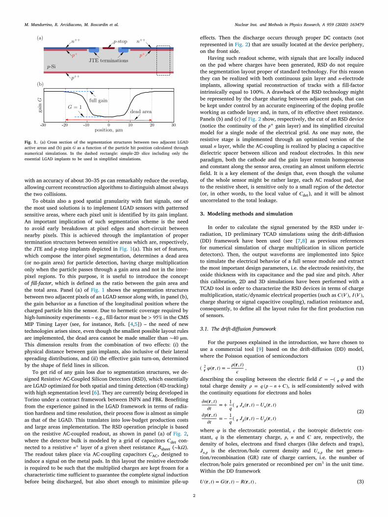
The last basic feature to be analyzed is the modeling sensitivity tothe gain layer doping dose and, in particular, the shift of the multiplica-tion onset towards low bias values with the increasing acceptor density.To this purpose, several 300 μm- and 50 μm-thick LGAD structuresrespectively coming from FBK and HPK, and (slightly) varying in theirmultiplication layer profiles, have been simulated. In the case of FBKdetectors, the dose increases for higher wafer numbers W while, inHPK sensors, the higher the letter progressively labeling the device thegreater the dopant dose. Again, both LGAD and p-i-n devices have beenimplemented.
As reported in Fig. 7, our numerical setup is perfectly sensitiveto dose variations in the gain layer. Moreover, both Massey andvan-Overstraeten–de Man formalisms well reproduce the experimentalcurves.
3.5. Electric field simulations
In the standard LGAD technology for particle tracking, one figure ofmerit to be carefully optimized with the simulator before designing thefinal detector layout is the electromagnetic insulation between sensitiveareas, i.e. at the level of inter-pixel termination structures, as well asin correspondence of the external guard region, designed to allow a
5

M. Mandurrino, R. Arcidiacono, M. Boscardin et al. Nuclear Inst. and Methods in Physics Research, A 959 (2020) 163479
Fig. 4. Comparison between measured (symbols) and simulated (lines) gain in unirradiated 50 μm-thick LGAD sensors by HPK as a function of (a) applied bias and (b) temperature.Experimental data taken at HPK and presented in Refs. [7,25].
Fig. 5. Measurements (symbols) and simulations (lines) of (a) charges versus bias in an irradiated 300 μm LGAD sensor by FBK and (b) bias to collect 20k electrons as a functionof fluence in 50 μm-thick LGAD sensors by HPK and CNM. Experimental data presented in Refs. [7,23,26].
Fig. 6. Unirradiated detectors. Panel (a): measured (symbols) and simulated (lines) 𝐶(𝑉 ) characteristics in Gallium and Boron carbonated 50 μm-thick LGAD from UFSD2 productionrun by INFN and FBK. Simulations are performed by generating electron/hole pairs with the heavy ion approach and by injecting a sinusoidal bias at 1 kHz. Panel (b): comparisonbetween experimental and numerical 𝐺(𝑉 ) characteristics for several UFSD2 devices.
correct scaling of bias voltage when the lithographic approach becomesmore aggressive. Moreover, as we have already seen in the previoussections, such traditional silicon detectors are affected by the signal (orgain) loss at the pixel periphery, so that a critical trade-off betweenlayout and efficiency has to be found.
We extensively explored such topics with numerical simulationswhen designing at INFN Torino, and in collaboration with FBK, the
last three runs of UFSD devices. And now we are facing with thenew challenges of optimizing our detectors in view of the upcomingproductions for the HL-LHC timing layers and within the RSD project.To this purpose, we have to abandon the simplified quasi-2D modelingscheme introduced in the previous section in favor of a more realisticsimulation framework, where all the oxide and metal layers have to
6
M. Mandurrino, R. Arcidiacono, M. Boscardin et al. Nuclear Inst. and Methods in Physics Research, A 959 (2020) 163479
Fig. 7. Room temperature comparison between measured (symbols) and simulated (lines) 𝐺(𝑉 ) characteristics in (a) 300 μm-thick LGAD detectors from UFSD1 production runby INFN and FBK (with the wafer number W increasing with the gain implant dose) and (b) 50 μm-thick LGAD devices by HPK (where, again, the last letter increases with theincreasing boron dose).
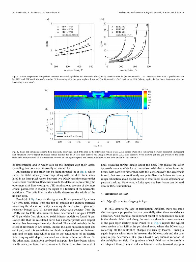
Fig. 8. Panel (a): simulated electric field (intensity color map) and drift lines in the inter-pixel region of an LGAD device. Panel (b): comparison between measured (histogram)and simulated (curve) signal amplitude versus position for an IR laser scan carried out along a 200 μm-pitch LGAD strip-detector. Note: pictures (a) and (b) are not to the samescale. (For interpretation of the references to color in this figure legend, the reader is referred to the web version of this article.)
be implemented and in which also all the implants with their lateralspreading functions are necessarily accounted for.
An example of this study can be found in panel (a) of Fig. 8, whichshows the field intensity color map, along with the drift lines, simu-lated in an inter-pixel region between two LGAD sensitive areas underreverse bias conditions. Red curves inside the detector, representing theoutermost drift lines closing on JTE terminations, are one of the mostcrucial parameters in shaping the signal as a function of the horizontalposition 𝑥. The drift lines in the middle determine the width of theno-gain area.
Panel (b) of Fig. 8 reports the signal amplitude generated by a laser(𝜆 = 1060 nm), shined from the top to emulate the charged particlestraversing the device vertically, scanning the inter-pixel region of areversely biased (230 V) 200 μm-pitch LGAD strip-detector from theUFSD2 run by FBK. Measurements have determined a no-gain FWHMof 75 μm while from simulation (with Massey model) we found 78 μm.Notice also that the calculated curve has a sharper profile with respectto what has been experimentally obtained. This could probably be theeffect of difference in two setups. Indeed, the laser has a finite spot size(∼15 μm), and this contributes to obtain a signal transition betweengain and no-gain zone which is due to the convolution of an electricfield, varying with depth, evaluated on a finite volume of silicon. Onthe other hand, simulations are based on a point-like laser beam, whichresults in a signal trend more conformal to the internal structure of drift
lines, revealing further details about the field. This makes the latterapproach more suitable for a comparison with data coming from testbeams with particles rather than with the laser. Anyway, the agreementis such that we can confidently use point-like simulations to have arough estimation about the fill-factor in traditional silicon detectors forparticle tracking. Otherwise, a finite spot size laser beam can be usedalso in TCAD simulations.
4. Simulation of RSD
4.1. Edge effects in the 𝑝+-type gain layer
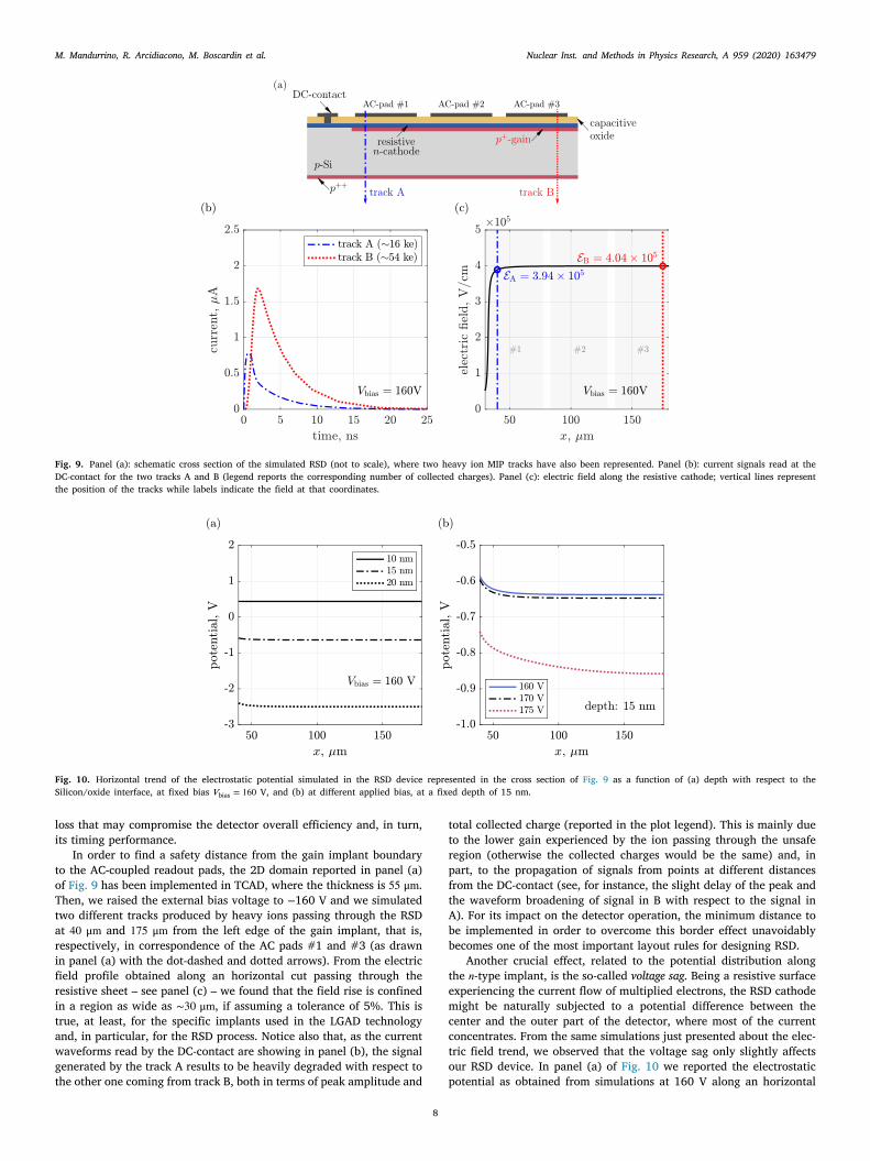
In RSD, despite the lack of termination implants, there are someelectromagnetic properties that can potentially affect the normal deviceoperation. As an example, an important aspect to be taken into accountis the electric field trend along the resistive sheet in correspondenceof the gain layer starting point. Panel (a) of Fig. 9 reports the typicalcross section of an RSD at its peripheral zone, where the DC-contactscollecting all the multiplied charges are usually located. Having a𝑝-gain implant which starts in between the DC-electrode and the cou-pling region determines (at a given bias) a longitudinal variation ofthe multiplication field. The gradient of such field has to be carefullyinvestigated through numerical simulations in order to avoid any gain
7
M. Mandurrino, R. Arcidiacono, M. Boscardin et al. Nuclear Inst. and Methods in Physics Research, A 959 (2020) 163479
Fig. 9. Panel (a): schematic cross section of the simulated RSD (not to scale), where two heavy ion MIP tracks have also been represented. Panel (b): current signals read at theDC-contact for the two tracks A and B (legend reports the corresponding number of collected charges). Panel (c): electric field along the resistive cathode; vertical lines representthe position of the tracks while labels indicate the field at that coordinates.
Fig. 10. Horizontal trend of the electrostatic potential simulated in the RSD device represented in the cross section of Fig. 9 as a function of (a) depth with respect to theSilicon/oxide interface, at fixed bias 𝑉bias = 160 V, and (b) at different applied bias, at a fixed depth of 15 nm.
loss that may compromise the detector overall efficiency and, in turn,its timing performance.
In order to find a safety distance from the gain implant boundaryto the AC-coupled readout pads, the 2D domain reported in panel (a)of Fig. 9 has been implemented in TCAD, where the thickness is 55 μm.Then, we raised the external bias voltage to −160 V and we simulatedtwo different tracks produced by heavy ions passing through the RSDat 40 μm and 175 μm from the left edge of the gain implant, that is,respectively, in correspondence of the AC pads #1 and #3 (as drawnin panel (a) with the dot-dashed and dotted arrows). From the electricfield profile obtained along an horizontal cut passing through theresistive sheet – see panel (c) – we found that the field rise is confinedin a region as wide as ∼30 μm, if assuming a tolerance of 5%. This istrue, at least, for the specific implants used in the LGAD technologyand, in particular, for the RSD process. Notice also that, as the currentwaveforms read by the DC-contact are showing in panel (b), the signalgenerated by the track A results to be heavily degraded with respect tothe other one coming from track B, both in terms of peak amplitude and
total collected charge (reported in the plot legend). This is mainly dueto the lower gain experienced by the ion passing through the unsaferegion (otherwise the collected charges would be the same) and, inpart, to the propagation of signals from points at different distancesfrom the DC-contact (see, for instance, the slight delay of the peak andthe waveform broadening of signal in B with respect to the signal inA). For its impact on the detector operation, the minimum distance tobe implemented in order to overcome this border effect unavoidablybecomes one of the most important layout rules for designing RSD.
Another crucial effect, related to the potential distribution alongthe 𝑛-type implant, is the so-called voltage sag. Being a resistive surfaceexperiencing the current flow of multiplied electrons, the RSD cathodemight be naturally subjected to a potential difference between thecenter and the outer part of the detector, where most of the currentconcentrates. From the same simulations just presented about the elec-tric field trend, we observed that the voltage sag only slightly affectsour RSD device. In panel (a) of Fig. 10 we reported the electrostaticpotential as obtained from simulations at 160 V along an horizontal
8

M. Mandurrino, R. Arcidiacono, M. Boscardin et al. Nuclear Inst. and Methods in Physics Research, A 959 (2020) 163479
cut located 10, 15 and 20 nm underneath the Silicon/oxide interface,i.e. through the resistive 𝑛-cathode. No voltage sag has to be noticedin these configurations (the slight decrease present within the first50 μm is directly related to the field rise observed in Fig. 9). If theexternal bias increases (see panel (b) of Fig. 10) and, in general,when we are approaching the breakdown voltage (about 175 V inthe simulation), the potential at a given depth progressively bends,producing a potential difference between AC-pad #1 and #3 of lessthan ∼100 mV (for a leakage current of some μA). This means that, forthe structure here considered and with the implants implemented, weare able to get rid of any sag effect when operating our RSD in a stableregime, i.e. suitably below the breakdown.
4.2. From spice-like to full-3D TCAD simulations of RSD
RSD simulations have been carried out in order to find the optimumrange of the most important design parameters, such as the dielectriccapacitance, the sheet resistance or the pad geometry. To this aim,Spice-like calculations accounting for the equivalent electrical modelof Fig. 2(a) have been implemented. By injecting into the circuitalnodes of the resistive sheet a test input signal – obtained through TCADsimulations of a 1D LGAD diode – one can read the output signalproduced by the simplified model in any other point of the same grid.
Fig. 11 shows two relevant results coming from this procedure,which have been simulated by parametrizing some of the characteristicRSD figures of merit: the pad size in panel (a) and the sheet resistance inpanel (b). In both graphs the same input signal has been injected (solidblack) while, in the first case, the capacitance of each node has beenchanged to emulate a parallel plate capacitor with constant thickness(at its technological standard for the FBK foundry) and area as indicatedby the legend. In the second case, the pad size has been kept fixed at500 × 500 μm2 and each resistor connecting two adjacent nodes hasbeen modulated from 0.5 kΩ to 2 kΩ. As one may appreciate, as the padsize or the sheet resistance increases, the output response read on thesame node (red dashed, dash-dotted and dotted curves) becomes higherin amplitude. We would like to stress that the test input signal weimplemented have been created and injected just to probe the circuitalproperties of RSD as a preliminary test before knowing any device’sfeature. Only the output pulses are calculated by Spice simulation.
Having obtained an indication of what would be the region ofinterest for our basic design parameters, full-TCAD simulations havebeen performed. When not otherwise specified, the technological rulesfor dielectric thickness and ion implantation are set as their foundrystandard to ensure an optimal AC-coupling. The first step consisted inimplementing the 2D geometry reported in Fig. 9(a), with a 55 μmthickness and pitch of 50 μm, and simulating the AC-signals induced onall the three readout pads by a MIP heavy ion passing perpendicularlyto the RSD and through the center of pad #1.
Fig. 12 reports the results of two different implant parametrizations.In panel (a) we tuned the 𝑝-gain dose by adding a 4% to the standardsetup. As the acceptor concentration increases the signal amplitudebecomes higher as well, without any significant modification of thepeak time. A similar result is reported in panel (b) for the tuning of the𝑛-cathode depth from the typical value to a deeper one. As one maynotice, all the waveforms are bipolar. Indeed, as occurring in standardLGAD-based detectors and as predicted by the Ramo’s theorem, thefirst lobe is due to the drift of multiplied electrons from the gainlayer to the detector surface. Then, since the AC readout pads in RSDdevices does not physically collect charges, when they move along thecathode towards the DC-contact, they produce an undershoot. Thus,the overall signal integral, given by both the induction and dischargecontributions, is always null.
In order to directly see the effects of having different couplingcapacitances, we simulated two RSD with the same features except forthe dielectric thickness: Fig. 13(a) reports the simulated signals for athin and a thick dielectric, showing that, as expected, the thinner thelayer the strongest the AC-coupling, albeit the effect is rather mild.
The same figure, in panel (b), shows the comparison between thethree usual signals simulated in 50 μm- and 100 μm-pitch devices. Wenotice that the signal induced in the readout pad where the particle hitsthe RSD sensor is larger when the pitch increases. In the case of the twonearest neighboring pads the signal waveforms tend to be longer butwith a lower amplitude, determining also a forward shift of the peak.Such spreading in time of the signals on pads #2 and #3 is essentiallydue to the increase of their dimension, which determines a longer pathfor charge carriers before being completely seen by the readout.
After characterizing the electrical properties of RSD devices as afunction of their technological parameters, it is useful to analyze thequality and the effectiveness of our simulations. In the framework ofLGAD design, the implementation of a full geometry becomes criticalonly when we are interested in investigating the extremal behavior ofthose structures, as the breakdown phenomena. For such a purpose theinclusion of guard regions is almost mandatory. Similarly, in RSD, arealistic modeling could help in identifying some fundamental figuresof merit such as, one among all, the capacitive coupling.
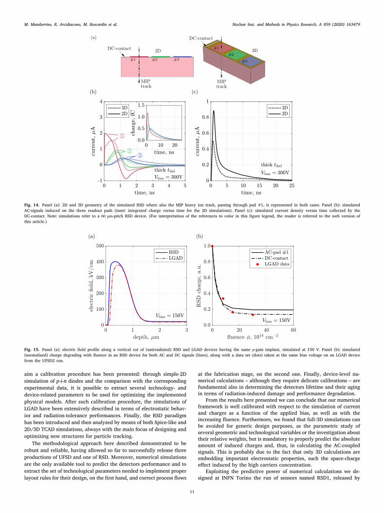
For these reasons now we want to answer the question: to whatextend the 3D simulation of RSD is necessary? To this aim, a 1 × 3structure as depicted on the right-hand side of Fig. 14(a) has beenimplemented. The rectangular metal region on top is, again, the DC-contact while colored square pads are the three AC-pads. On its left,the usual 2D version of the same RSD is reported for reference. In bothstructures the MIP heavy ion crosses the device perpendicularly to thecentral point of pad #1 (leftmost red pad).
As one may see in Fig. 14, the full-3D simulation gives a lower andbroadened (in time) signal with respect to the 2D geometry, both interms of AC- and DC-current. This can be probably due to the space-charge effect, not accounted for by the 2D simulation, caused by thehigh density of charges populating the resistive sheet during the signalfreezing time. So, if by the standpoint of coupling properties the full-3D simulation results to be the only possible investigation, on the otherhand, the parametric studies about all the RSD design and process rulesare feasible just through the simple 2D geometry.
The last two topics that the authors want to report are a comparisonbetween RSD and LGAD simulations, on one side, and the predictedperformances of RSD in terms of radiation tolerance and acceptor deac-tivation, on the other one. The plots showing such results are reportedin Fig. 15. Panel (a) includes a direct comparison between the electricprofiles along the device vertical cut simulated in an LGAD and an RSDat the same bias voltage (150 V), and with the same 𝑝-gain implants.What we can infer is that, for a given gain layer concentration anddue to the different 𝑛-cathode implant with respect to the traditionaltechnology, the multiplication occurs closer to the silicon surface in theRSD than in the LGAD. Moreover, the field intensity is higher for thefirst device, probably leading to more critical breakdown voltages withrespect to the traditional silicon technology for 4D particle tracking.
To explore the radiation tolerance of RSD and the degradation ofsignals with fluence, in case of their use for 4D-tracking inradiation-intense environments, 2D numerical simulations have beencarried out. By implementing both the creation of acceptor-like trapsin the bulk (which acts on the detector resistivity) and the Borondeactivation in the gain layer – as modeled by Eq. (11) – the resultsshown in Fig. 15(b) have been obtained. As usual, simulated signalsare triggered by a MIP heavy ion crossing the device in the center ofthe AC-pad #1, the same in which the charge is read. In the case ofAC-coupled signals, only the positive lobe of the current waveform hasbeen accounted for in calculating the induced charge, while for the DC-contact the entire signal shape has been integrated in time. Notice thatthe radiation resistance at high fluence corresponding to the capacitivecoupling is sightly better than the trend obtained for the traditional DCreadout, where less than the 20% of the original signal survives beyond1015 neq/cm2. Such behavior is quite well matching the experimentaldata coming from a UFSD2 sample with the same 𝑝-gain implant. Thisresult could be interpreted as the effect of having a higher electric fieldin the RSD compared to the corresponding LGAD, as shown in the samefigure.
9

M. Mandurrino, R. Arcidiacono, M. Boscardin et al. Nuclear Inst. and Methods in Physics Research, A 959 (2020) 163479
Fig. 11. RSD response (red curves) of a TCAD-like input signal (solid black) simulated with Spice as a function of (a) the AC-pad size and (b) sheet resistance. The signal isinjected and read on the same node of the resistive grid, as represented in the electrical model of Fig. 2(a).
Fig. 12. TCAD simulations of AC-coupled signals generated in a 50 μm-pitch three-pad RSD sensor (the circled numbers identify the position of the pad, from left to right) bya MIP heavy ion for (a) two 𝑝-gain doses and (b) 𝑛-cathode depths. The parametric setup is the standard one in the right plot while in the first one a thick dielectric has beenimplemented.
Fig. 13. TCAD simulations of AC-coupled signals generated in a 50 μm-pitch three-pad RSD sensor (the circled numbers identify the position of the pad, from left to right) by aMIP heavy ion for (a) two dielectric thicknesses and (b) pad pitches. The parametric setup is the standard one in the left plot while in the second one a thick dielectric has beenimplemented.
5. Comments and conclusions
In this paper, advanced and reliable techniques to model and char-acterize silicon particle detectors for 4D-tracking through device-levelnumerical simulation have been reviewed. As a case-study we analyzed
the LGAD technology and, in particular, the RSD sensors. After asummary of the main devices figures of merit, we moved to the frame-work of Technology Computer-Aided Design (TCAD) physics-basednumerical simulation, giving some relevant examples of its powerfulcapabilities in predicting the electrical behavior of real devices. To this
10
M. Mandurrino, R. Arcidiacono, M. Boscardin et al. Nuclear Inst. and Methods in Physics Research, A 959 (2020) 163479
Fig. 14. Panel (a): 2D and 3D geometry of the simulated RSD where also the MIP heavy ion track, passing through pad #1, is represented in both cases. Panel (b): simulatedAC-signals induced on the three readout pads (inset: integrated charge versus time for the 2D simulations). Panel (c): simulated current density versus time collected by theDC-contact. Note: simulations refer to a 60 μm-pitch RSD device. (For interpretation of the references to color in this figure legend, the reader is referred to the web version ofthis article.)
Fig. 15. Panel (a): electric field profile along a vertical cut of (unirradiated) RSD and LGAD devices having the same 𝑝-gain implant, simulated at 150 V. Panel (b): simulated(normalized) charge degrading with fluence in an RSD device for both AC and DC signals (lines), along with a data set (dots) taken at the same bias voltage on an LGAD devicefrom the UFSD2 run.
aim a calibration procedure has been presented: through simple-2Dsimulation of p-i-n diodes and the comparison with the correspondingexperimental data, it is possible to extract several technology- anddevice-related parameters to be used for optimizing the implementedphysical models. After such calibration procedure, the simulations ofLGAD have been extensively described in terms of electrostatic behav-ior and radiation-tolerance performances. Finally, the RSD paradigmhas been introduced and then analyzed by means of both Spice-like and2D/3D TCAD simulations, always with the main focus of designing andoptimizing new structures for particle tracking.
The methodological approach here described demonstrated to berobust and reliable, having allowed so far to successfully release threeproductions of UFSD and one of RSD. Moreover, numerical simulationsare the only available tool to predict the detectors performance and toextract the set of technological parameters needed to implement properlayout rules for their design, on the first hand, and correct process flows
at the fabrication stage, on the second one. Finally, device-level nu-merical calculations – although they require delicate calibrations – arefundamental also in determining the detectors lifetime and their agingin terms of radiation-induced damage and performance degradation.
From the results here presented we can conclude that our numericalframework is well calibrated with respect to the simulation of currentand charges as a function of the applied bias, as well as with theincreasing fluence. Furthermore, we found that full-3D simulations canbe avoided for generic design purposes, as the parametric study ofseveral geometric and technological variables or the investigation abouttheir relative weights, but is mandatory to properly predict the absoluteamount of induced charges and, thus, in calculating the AC-coupledsignals. This is probably due to the fact that only 3D calculations areembedding important electrostatic properties, such the space-chargeeffect induced by the high carriers concentration.
Exploiting the predictive power of numerical calculations we de-signed at INFN Torino the run of sensors named RSD1, released by
11

M. Mandurrino, R. Arcidiacono, M. Boscardin et al. Nuclear Inst. and Methods in Physics Research, A 959 (2020) 163479
FBK in June 2019 and currently under testing. This production willbe the definite workbench of our methodological approach and, in themeanwhile, will also represent the basis for both a characterization ofa novel kind of 4D particle trackers and their optimization in view ofa following production run.
Declaration of competing interest
The authors declare that they have no known competing finan-cial interests or personal relationships that could have appeared toinfluence the work reported in this paper.
CRediT authorship contribution statement
M. Mandurrino: Conceptualization, Methodology, Software, Vali-dation, Formal analysis, Investigation, Resources, Data curation, Writ-ing - original draft, Writing - review & editing, Visualization, Projectadministration, Funding acquisition. R. Arcidiacono: Validation, Re-sources. M. Boscardin: Resources. N. Cartiglia: Conceptualization,Methodology, Validation, Investigation, Resources, Writing - review &editing, Funding acquisition. G.-F. Dalla Betta: Investigation, Writ-ing - review & editing. M. Ferrero: Investigation, Data curation. F.Ficorella: Investigation, Data curation. L. Pancheri: Investigation,Writing - review & editing. G. Paternoster: Investigation, Data cura-tion. F. Siviero: Investigation, Data curation. V. Sola: Investigation,Data curation. A. Staiano: Investigation. A. Vignati: Investigation.
Acknowledgments
This work and the RSD project are supported by INFN, Italy Gruppo-V through the ‘‘2017 Young Researchers Grant’’ funding program (asin the INFN announcement No. 19105 and the related deliberation No.19567). The authors would also thank the RD50 Collaboration at CERNand UC Santa Cruz for the scientific endorsement.
Appendix. Parameters for the modeling of charge multiplication
Now we describe how the electron/hole impact ionization coeffi-cients 𝛼𝑛,𝑝 are parametrized for all the three models here employedin the numerical implementation of avalanche processes. By defini-tion, 𝛼𝑛,𝑝 (in cm−1) corresponds to the inverse of the electron/holemean free path between two subsequent scattering events, which giverise to the impact ionization of lattice atoms. When the field drivingcharge carriers becomes such that this process cannot be naturallydamped anymore, and carriers overcome a certain critical velocity, thenthe avalanche multiplication starts. The coefficients 𝛼𝑛,𝑝 describe in amacroscopic scale such mechanism, being the representation of how themean free path decreases as a function of the increasing electric field.
As we have seen in the previous sections, the ionization coeffi-cients follow the so-called Chynoweth law [13], where the exponentialgrowth is multiplied by a certain pre-factor. According to the physicalmodel, each term has a particular parametrization, coming from differ-ent experimental data taken on different samples of silicon devices. Inparticular, for the Massey formula [10] we have that
𝐴Mas𝑛 = 4.43 ⋅ 105 cm−1
𝐴Mas𝑝 = 1.13 ⋅ 106 cm−1 (14)
and𝐵Mas𝑛 (𝑇 ) = 𝐶Mas
𝑛 +𝐷Mas𝑛 ⋅ 𝑇
𝐵Mas𝑝 (𝑇 ) = 𝐶Mas
𝑝 +𝐷Mas𝑝 ⋅ 𝑇
(15)
where𝐶Mas𝑛 = 9.66 ⋅ 105 V/cm
𝐶Mas𝑝 = 1.71 ⋅ 106 V/cm
(16)
and𝐷Mas
𝑛 = 4.99 ⋅ 102 V cm−1 K−1
𝐷Mas𝑝 = 1.09 ⋅ 103 V cm−1 K−1 . (17)
In the same way, we have the parameters for van Overstraeten–deMan [11]
𝐴vOv𝑛 = 7.030 ⋅ 105 cm−1
𝐵vOv𝑛 = 1.231 ⋅ 106 V/cm
, (18)
𝐴vOv𝑝 = 1.582 ⋅ 106 cm−1 (below 4 ⋅ 105 V/cm)
𝐵vOv𝑝 = 2.036 ⋅ 106 V/cm (below 4 ⋅ 105 V/cm)
𝐴vOv𝑝 = 6.710 ⋅ 105 cm−1 (above 4 ⋅ 105 V/cm)
𝐵vOv𝑝 = 1.693 ⋅ 106 V/cm (above 4 ⋅ 105 V/cm)
(19)
and
𝛾 =tanh
( ℏ𝜔op2𝑘B300K
)
tanh( ℏ𝜔op2𝑘B𝑇
) , (20)
where ℏ𝜔op = 0.063 eV is the optical phonon energy in silicon, and forthe Okuto–Crowell model [12]
𝐴Oku𝑛 = 0.426V−1
𝐴Oku𝑝 = 0.243V−1
𝐵Oku𝑛 = 4.81 ⋅ 105 V/cm
𝐵Oku𝑝 = 6.53 ⋅ 105 V/cm
(21)
and𝐶Oku𝑛 = 3.05 ⋅ 10−4 K−1
𝐶Oku𝑝 = 5.35 ⋅ 10−4 K−1
𝐷Oku𝑛 = 6.86 ⋅ 10−4 K−1
𝐷Oku𝑝 = 5.67 ⋅ 10−4 K−1
. (22)
References
[1] N. Cartiglia, et al., Design optimization of UFSD silicon detectors, Nucl. Instrum.Methods Phys. Res. A 796 (2015) 141–148, http://dx.doi.org/10.1016/j.nima.2015.04.025.
[2] H.F.-W. Sadrozinski, A. Seiden, N. Cartiglia, 4D tracking with ultra-fast silicondetectors, Rep. Progr. Phys. 81 (2018) 026101, http://dx.doi.org/10.1088/1361-6633/aa94d3.
[3] N. Cartiglia, et al., Beam test results of a 16ps timing system based on ultra-fast silicon detectors, Nucl. Instrum. Methods Phys. Res. A 850 (2017) 83–88,http://dx.doi.org/10.1016/j.nima.2017.01.021.
[4] CMS Collaboration, Technical proposal for a MIP timing detector in the CMSexperiment Phase 2 upgrade, CERN-LHCC-2017-027; LHCC-P-009.
[5] J. Bendavid, MIP timing detector for CMS phase-II upgrade, in: CMS MTDMeeting, CERN, 2018.
[6] M. Mandurrino, et al., First demonstration of 200, 100, and 50 μm pitch resistiveAC-coupled silicon detectors (RSD) with 100% fill-factor for 4D particle tracking,2019, arXiv:1907.03314.
[7] M. Mandurrino, et al., TCAD simulation of silicon detectors: A validation toolfor the development of LGAD, in: 30th RD50 Workshop, Kraków, 2017.
[8] M. Mandurrino, et al., Numerical simulation of charge multiplication in ultra-fastsilicon detectors and comparison with experimental data, in: 2017 IEEE NuclearScience Symposium and Medical Imaging Conference, NSS/MIC, Atlanta, 2017,http://dx.doi.org/10.1109/NSSMIC.2017.8532702.
[9] Sentaurus Device User Guide, Version N-2017.09, Synopsys, Inc., Mountain View,CA, 2017.
[10] D.J. Massey, J.P.R. David, G.J. Rees, Temperature dependence of impact ion-ization in submicrometer silicon devices, IEEE Trans. Electron Devices 53 (9)(2006) 2328–2334, http://dx.doi.org/10.1109/TED.2006.881010.
[11] R. van Overstraeten, H. de Man, Measurement of the ionization rates in diffusedsilicon p–n junctions, Solid-State Electron. 13 (5) (1970) 583–608, http://dx.doi.org/10.1016/0038-1101(70)90139-5.
[12] Y. Okuto, C.R. Crowell, Threshold energy effect on Avalanche breakdown voltagein semiconductor junctions, Solid-State Electron. 18 (2) (1975) 161–168, http://dx.doi.org/10.1016/0038-1101(75)90099-4.
[13] A.G. Chynoweth, Ionization rates for electrons and holes in silicon, Phys. Rev.109 (5) (1958) 1537–1540, http://dx.doi.org/10.1103/PhysRev.109.1537.
12

M. Mandurrino, R. Arcidiacono, M. Boscardin et al. Nuclear Inst. and Methods in Physics Research, A 959 (2020) 163479
[14] B.R. Gossick, Disordered regions in semiconductors bombarded by fast neutrons,J. Appl. Phys. 30 (8) (1959) 1214–1218, http://dx.doi.org/10.1063/1.1735295.
[15] G. Kramberger, et al., Radiation effects in low gain Avalanche detectors afterhadron irradiations, J. Inst. 10 (7) (2015) P07006, http://dx.doi.org/10.1088/1748-0221/10/07/P07006.
[16] G.D. Watkins, EPR studies of lattice defects in semiconductors, in: B. Henderson,A.E. Hughes (Eds.), Defects and their structure in non-metallic solids, Plenum,New York, 1976, http://dx.doi.org/10.1007/978-1-4684-2802-5_7.
[17] R. Wunstorf, W.M. Bugg, J. Walter, F.W. Garber, D. Larson, Investigations ofdonor and acceptor removal and long term annealing in silicon with differentboron/phosphorus ratios, Nucl. Instrum. Methods A 377 (1–2) (1996) 228–233,http://dx.doi.org/10.1016/0168-9002(96)00217-3.
[18] J.P. Balbuena, et al., RD50 Status Report 2008 - Radiation hard semiconductordevices for very high luminosity colliders, CERN-LHCC-2010-012; LHCC-SR-003,CERN, Geneva, 2008, URL: http://cds.cern.ch/record/1291631.
[19] M. Ferrero, et al., Radiation resistant LGAD design, Nucl. Instrum. Methods A919 (2019) 16–26, http://dx.doi.org/10.1016/j.nima.2018.11.121.
[20] W. Shockley, Currents to conductors induced by a moving point charge, J. Appl.Phys. 9 (10) (1938) 635–636, http://dx.doi.org/10.1063/1.1710367.
[21] S. Ramo, Currents induced by electron motion, Proc. IRE 27 (9) (1939) 584–585,http://dx.doi.org/10.1109/JRPROC.1939.228757.
[22] G. Kramberger, et al., Radiation hardness of thin low gain Avalanche detectors,Nucl. Instrum. Methods Phys. Res. A 891 (2018) 68–77, http://dx.doi.org/10.1016/j.nima.2018.02.018.
[23] G. Kramberger, Results and plans on irradiated LGAD sensors, in: HighGranularity Timing Detector (HGTD) Meeting, CERN, 2017.
[24] V. Eremin, et al., Development of transient current and charge techniques forthe measurement of effective net concentration of ionized charges (𝑁eff) in thespace charge region of p–n junction detectors, Nucl. Instrum. Methods Phys. Res.A 372 (3) (1993) 388–398, http://dx.doi.org/10.1016/0168-9002(95)01295-8.
[25] H.F.-W. Sadrozinski, Timing measurements on ultra-fast silicon detectors, in: 12thTrento Workshop on Advanced Silicon Radiation Detectors, Trento, 2017.
[26] G. Kramberger, Radiation hardness of thin LGAD detectors, in: 12th TrentoWorkshop on Advanced Silicon Radiation Detectors, Trento, 2017.
[27] V. Sola, et al., First FBK production of 50μm ultra-fast silicon detectors, Nucl.Instrum. Methods Phys. Res. A 924 (2019) 360–368, http://dx.doi.org/10.1016/j.nima.2018.07.060.
13