Embed Size (px)
Citation preview

Analysis and Design of MultioutputFlyback Converter
A study For A Lab Upgrade on the Flyback converter assignment atChalmers Elteknik
Master’s thesis in Electric Power Engineering
Abdi AhmedAbdullahi Kosar
Department of Energy & EnvironmentChalmers University of TechnologyGothenburg, Sweden 2016

Master’s thesis 2016:ENM
Analysis and Design of Multioutput FlybackConverter
A study For A Lab Upgrade on the Flyback converter assignmentat Chalmers Elteknik
ABDI AHMEDABDULLAHI KOSAR
Department of Energy & EnvironmentDivision of Electric Power Engineering
Chalmers University of TechnologyGothenburg, Sweden 2016

Analysis and Design of Multioutput Flyback ConverterMaster’s thesis 2016:ENMABDI AHMEDABDULLAHI KOSAR
c© ABDI AHMEDABDULLAHI KOSAR, 2016.
Department of Energy & EnvironmentDivision of Electric Power EngineeringChalmers University of TechnologySE–412 96 GothenburgSwedenTelephone +46 (0)31–772 1000
Cover:Multi-output flyback converter prototype PCB
Chalmers ReproserviceGothenburg 2016

Analysis and Design of Multioutput Flyback ConverterMaster’s thesis 2016:ENMABDI AHMEDABDULLAHI KOSARDepartment of Energy & EnvironmentDivision of Electric Power EngineeringChalmers University of Technology
Abstract
This thesis work is done in order to improve the existing lab in Chalmers forthe study of Power Electronics. Assignments for the practical lab and computersimulation sessions of a flyback converter have been reviewed and analysed. Theanalyses of the existing assignments shows that the circuit board used in the labtoday is a multi purpose circuit and it is difficult to relate a equivalent circuitdiagram of a flyback converter. Furthermore, there is no relationship between thecircuit and the simulation model.
A simulation was done using PSpice and a prototype PCB board built with the aimof showing some of these interesting concepts in the course. The main suggestionsare related to the simplification of the circuits so that immediate correlation can bemade between the circuits being shown in the class and the PCB used in the lab.The simulation model can be used in the simulation session of the course.
The new simulation model and the circuit board can demonstrate the role of theinductor in the flyback transformer by varying its value. Another area of improve-ment would be on demonstrating of magnetics theory. There is no simulation orpractical assignments about magnetics in the course today. Understanding the re-lation between the current ripple and magnetic flux is in the scope of the courses.It is also important to understand how high frequency affects the losses and thesize of the core. Two transformers are designed in order to investigate these rela-tionships. The result of the transformer design shows that a new assignment thatcan demonstrate how magnetic core behaves can be introduced.
Keywords: Flyback, Multi-output, DCM,CCM, LM5020,Switch modepower supply
v


Acknowledgement
First of all we would like to thank the Almighty for making this possible. Thecontributions we had from our supervisor Andreas Henriksson were numerous andimmesuarable and we would like to acknowledge his commitment and effort inenabling this work. Of notable mention is Altran, Ericsson and Chalmers whowere the collaborating partners.
Encouragement and support from our family members and friends will not gounappreciated. Thank you.
Finally, Abdullahi would like to acknowledge the Swedish Institute for the generousscholarship for his master’s studies.
Abdi & Abdullahi
Gothenburg, September 27, 2016


Contents
Abstract v
Acknowledgments vii
Contents ix
List of Figures xi
List of Tables xiv
Abbreviations xv
1 Introduction 11.1 Background . . . . . . . . . . . . . . . . . . . . . . . . . . . . . . . 11.2 Problem . . . . . . . . . . . . . . . . . . . . . . . . . . . . . . . . . 21.3 Purpose . . . . . . . . . . . . . . . . . . . . . . . . . . . . . . . . . 31.4 Scope . . . . . . . . . . . . . . . . . . . . . . . . . . . . . . . . . . 3
2 Pedagogic Background 52.1 Existing Flyback Lab for ENM060 . . . . . . . . . . . . . . . . . . 62.2 Existing Simulation Task for flyback in ENM060 . . . . . . . . . . . 72.3 Suggestions . . . . . . . . . . . . . . . . . . . . . . . . . . . . . . . 8
3 Technical Background 113.1 Circuit Description . . . . . . . . . . . . . . . . . . . . . . . . . . . 123.2 Operating Modes . . . . . . . . . . . . . . . . . . . . . . . . . . . . 13
3.2.1 CCM mode of operation . . . . . . . . . . . . . . . . . . . . 143.2.2 DCM mode of operation . . . . . . . . . . . . . . . . . . . . 163.2.3 Boundary between CCM and DCM . . . . . . . . . . . . . . 18
ix

CONTENTS
3.3 Magnetics . . . . . . . . . . . . . . . . . . . . . . . . . . . . . . . . 203.3.1 Characteristic of a magnetic core . . . . . . . . . . . . . . . 213.3.2 Effect of Air gap . . . . . . . . . . . . . . . . . . . . . . . . 23
3.4 Control circuit of the flyback . . . . . . . . . . . . . . . . . . . . . 24
4 Design and simulation of the model 274.1 System specifications . . . . . . . . . . . . . . . . . . . . . . . . . . 274.2 Determination of Maximum duty ratio (Dmax) . . . . . . . . . . . . 294.3 Transformers primary inductance (Lm) . . . . . . . . . . . . . . . . 314.4 Core selection . . . . . . . . . . . . . . . . . . . . . . . . . . . . . . 32
4.4.1 Determine the maximum flux swing (∆Bmax) . . . . . . . . 364.4.2 Calculate windows area product AP . . . . . . . . . . . . . . 364.4.3 Determine the required number of minimum primary turns
Nminp . . . . . . . . . . . . . . . . . . . . . . . . . . . . . . . 37
4.5 Determing the Secondary Turns . . . . . . . . . . . . . . . . . . . . 374.6 Determing the Wire Diameter . . . . . . . . . . . . . . . . . . . . . 394.7 Choosing the diodes . . . . . . . . . . . . . . . . . . . . . . . . . . 404.8 Determine the output capacitors . . . . . . . . . . . . . . . . . . . . 414.9 Design of Clamp and Damping circuit . . . . . . . . . . . . . . . . . 424.10 Compensator Design . . . . . . . . . . . . . . . . . . . . . . . . . . 44
5 Simulation and PCB Design of a Flyback 475.1 Existing Simulation Model . . . . . . . . . . . . . . . . . . . . . . 475.2 Proposed Simulation Model . . . . . . . . . . . . . . . . . . . . . . 485.3 PCB Design . . . . . . . . . . . . . . . . . . . . . . . . . . . . . . . 49
5.3.1 Current Measuring . . . . . . . . . . . . . . . . . . . . . . . 51
6 Simulations and Measurements 536.1 Simulations . . . . . . . . . . . . . . . . . . . . . . . . . . . . . . . 53
6.1.1 Inductance value in CCM . . . . . . . . . . . . . . . . . . . 536.1.2 Inductance value in DCM . . . . . . . . . . . . . . . . . . . 546.1.3 Current sense simulations . . . . . . . . . . . . . . . . . . . 556.1.4 Compensation Network . . . . . . . . . . . . . . . . . . . . . 56
6.2 Measurements . . . . . . . . . . . . . . . . . . . . . . . . . . . . . . 57
7 Results 59
8 Discussion 63
9 Conclusion and Future Work 659.1 Conclusion . . . . . . . . . . . . . . . . . . . . . . . . . . . . . . . 659.2 Future Work . . . . . . . . . . . . . . . . . . . . . . . . . . . . . . . 66
x

CONTENTS
Bibliography 68
A Derivations of the mathematical equations A1A.1 Converter . . . . . . . . . . . . . . . . . . . . . . . . . . . . . . . . A1A.2 Control . . . . . . . . . . . . . . . . . . . . . . . . . . . . . . . . . A2A.3 Filter . . . . . . . . . . . . . . . . . . . . . . . . . . . . . . . . . . . A2A.4 Matlab code for compensation network . . . . . . . . . . . . . . . . A2
B Data sheets A1B.1 N87 datasheet . . . . . . . . . . . . . . . . . . . . . . . . . . . . . . A1
xi

CONTENTS
xii

List of Figures
3.1 Circuit diagram of the flyback converter . . . . . . . . . . . . . . . 123.2 Equivalent Circuit of flyback converter.(a) When the switch is on
and the diode is blocking.(b) When the diode is forward biased andthe switch is off. . . . . . . . . . . . . . . . . . . . . . . . . . . . . 13
3.3 Voltage and current wave forms of flyback converter working on CCM 143.4 Current and Voltage wave forms of the flyback converter working in
DCM. . . . . . . . . . . . . . . . . . . . . . . . . . . . . . . . . . . 173.5 Voltage and current wave forms of a flyback converter working on
BCM . . . . . . . . . . . . . . . . . . . . . . . . . . . . . . . . . . . 183.6 Normalized output current Io at the boundary as a function of duty
cycle (D) for a flyback converter. . . . . . . . . . . . . . . . . . . . 203.7 Relationships between the electrical and magnetic quantities . . . . 203.8 B-H loop . . . . . . . . . . . . . . . . . . . . . . . . . . . . . . . . . 223.9 Hysteresis in the B-H plane for ferromagnetic cores. Dashed line;
with air-gap Solid line;with no air-gap . . . . . . . . . . . . . . . . 243.10 Type II error amplifier . . . . . . . . . . . . . . . . . . . . . . . . . 26
4.1 flow chart of design procedure[1] . . . . . . . . . . . . . . . . . . . . 284.2 Switch and diode utilization factor versus duty cycle of a flyback. . 304.3 Relative core losses versus frequency for N87 core material . . . . . 344.4 Primary inductor mode current, blue for DCM and red for CCM . . 354.5 Hysteresis in the B-H plane for ferromagnetic cores.(a) typical fly-
back operating in CCM.(b) typical flyback operating in DCM . . . 354.6 An ideal diagram of the transformer . . . . . . . . . . . . . . . . . . 384.7 (a)Output capacitor current.(b) Simple circuit diagram of the out-
put capacitor, diode and load . . . . . . . . . . . . . . . . . . . . . 424.8 Circuit showing the arrangement of a TVS and diode to achieve
clamping . . . . . . . . . . . . . . . . . . . . . . . . . . . . . . . . 43
xiii

LIST OF FIGURES
4.9 Voltage across the MOSFET: (a) Without clamp (b) With clamp(c) with clamp and damping resistance and capacitor . . . . . . . . 43
4.10 Equivalent circuit of a flyback converter.(a) ON mode (b) OFFmode. . . . . . . . . . . . . . . . . . . . . . . . . . . . . . . . . . . 44
4.11 Theoretical bode plot of the system . . . . . . . . . . . . . . . . . . 45
5.1 The existing simulation model. . . . . . . . . . . . . . . . . . . . . 475.2 Simulation model of a flyback converter with two outputs . . . . . . 485.3 Top Silkscreen . . . . . . . . . . . . . . . . . . . . . . . . . . . . . 505.4 Top copper trace . . . . . . . . . . . . . . . . . . . . . . . . . . . . 515.5 Bottom Copper . . . . . . . . . . . . . . . . . . . . . . . . . . . . . 51
6.1 Simulation: Current waveforms in a flyback converter operating inCCM mode with different input voltages: (a) Vd=15 (b) Vd=30. . . 54
6.2 Current waveforms in a flyback converter operating in DCM modewith different input voltages: (a) Vd=30 (b) Vd=15. . . . . . . . . . 55
6.3 Simulation: Current waveforms in a flyback converter operating inDCM mode with different input voltages: (a) Vd=15 (b) Vd=30. . . 56
6.4 Current measurement in the simulation model . . . . . . . . . . . . 566.5 Transient responte of the output voltage: (a) When load-step is
applied at input 1 (b) When load-step applied at input 2 . . . . . . 576.6 Measured result . . . . . . . . . . . . . . . . . . . . . . . . . . . . . 586.7 Drain Voltage with lower inductance value . . . . . . . . . . . . . . 58
7.1 Overview of the circuit board compered to the circuit diagram ofthe flyback converter. . . . . . . . . . . . . . . . . . . . . . . . . . . 60
7.2 Overview of two transformer with two different frequencies. Thefrequency of the large and small transformers are 65 and 300 kHzrespectively . . . . . . . . . . . . . . . . . . . . . . . . . . . . . . . 61
xiv

List of Tables
4.1 System specification . . . . . . . . . . . . . . . . . . . . . . . . . . 294.2 The RMS value of the current and the resulting primary inductance 324.3 Core list and design properties . . . . . . . . . . . . . . . . . . . . . 334.4 Number of turns and core type . . . . . . . . . . . . . . . . . . . . 384.5 Copper diameter and their current carrying capacity for different
A/cm2 . . . . . . . . . . . . . . . . . . . . . . . . . . . . . . . . . . 404.6 Rms value of the current and the required number of wires . . . . . 404.7 Ratings of the power stage components . . . . . . . . . . . . . . . . 42
xv

LIST OF TABLES
xvi

1
Introduction
1.1 Background
Power electronic converters is a common object in today’s electronic world andfor a very good reason. With quite a bit of interest in smaller sized consumerproducts and energy efficiency, there is a need for power supplies to adapt
to these needs. The evolution of power supplies, as does many other electronicitems, follows a trend that ends up with better and more efficient designs.
The need to control power more efficiently and reduce losses coupled with theimprovement and advancement of power electronic switches led to the adoption ofswitched mode power supplies (SMPS). The main principle being that the inputis connected to the energy storage devices (capacitors and inductors) only as longas it is required; not all the time as is with the case of linear regulators. Powerelectronic switches that can be switched as fast as several MHz enables this.
A switch mode power supply has a high efficiency which reaches up to 90 %. Thehigh efficiency eliminates the need for big heat sinks and therefore the size and costof the power supply decreases significantly. For this reason, a SMPS is preferredto use in situations where a high supply efficiency is necessary [2]. Some of theareas where this technology is applicable is in battery-powered and hand-heldapplications where the battery lifetime and the temperature are essential [3]. Thedisadvantages of an SMPS are minor and can be overcome with a proper design.However, switched mode power supply design is inherently a time consuming jobrequiring many trade-offs and a large number of design variables.
Power electronics is one of the four major areas taught to electrical power engineer-ing students at Chalmers University of Technology. The main reason being that it
1

1.2. PROBLEM Chapter 1
is an area that has wide applications and require some level of familiarity to futureelectrical engineers. Two courses (Power Electronic Converters (ENM060 ) andPower Electronic Devices and Applications (ENM070 ) deal with a wide range ofapplications in terms of power and the students carry out lab activities in these twocourses. The aim of this thesis is to upgrade the lab exercises and the equipmentused in these labs ,in particular the practical lab for the flyback converter.
There are several reasons that make it necessary to upgrade the current lab equip-ment. The lectures are based on simplified circuits while the existing circuit boardcontains many more components making the correlation difficult for the students.From a pedagogical point of view, it would be easier for the students to have asimple circuit with fewer components on it. Therefore, it is proposed in this re-port to design a simple flyback converter which can be easily compared to thematerial shown in the lectures. Another important demonstration will be to showthe effects of different switching frequencies. The size of a switching power supplydecreases as the switching frequency increases, but a high frequency also comeswith high switching losses. In this thesis it is proposed to design two converterseach with a different switching frequency to give the students an insight into howthe frequency affects the different design parameters.
1.2 Problem
The laboratory sessions are aimed at giving a practical glimpse of some of theconcepts that have been discussed in the lectures. The aim being, especially inthe introductory courses, to give the student appreciation of some of the mostimportant elements in the course. The laboratory exercise should give the studentthe possibility to see the concepts come to life without necessarily bogging thestudent down with details. It should however not abstract the workings so muchas to turn it into another theoretical exercise. A fine balance has thus to be struckbetween simplicity and function.
The introductory elements which are most important to show in a practical lab andthe best laboratory arrangement that is able to show these fundamental conceptsis the aim of this thesis.
2

1.3. PURPOSE Chapter 1
1.3 Purpose
The purpose of this thesis is to investigate the lab tasks that could be interestingfor the students and the best way to link the lectures to the lab. A prototypecircuit will be built in an attempt to show some of the interesting concepts inthe study of power electronics. The thesis specifically deals with investigating amultiple output flyback converter. The design task will be to come up with a circuitthat will display some of the fundamentals of a flyback converter. The design willfirst be done by calculations, then simulated and finally a working circuit will becreated, tested and characterized.
1.4 Scope
The design task will be aimed at coming up with a working model that can displaysome of the most important fundamentals. Due to the nature of the the thesis,optimizations with regards to losses and EMI will not be a priority. There arealso limitations in regards to the existing power supply in the lab which also setsa limit on the maximum size of the converter that is to be built. The existingpower supply in the lab is rated 30V/2.5A which sets the limit for the flybackdesign.
The design will feature a multiple output design with one of the outputs being themaster. There are many ways to achieve cross regulation and this thesis will notbe overly interested with stabilizing the slave output beyond setting a large designmargin.
The feedback will not be isolated since it requires other components such as anoptocoupler. The design will be as simple as possible and the use of non-isolatedfeedback for this particular task will be safe due to the low power range of theconverter.
The choice of control strategy between voltage and current control will be basedon the chosen controller. In this design, current mode control will be chosen andthe choice is motivated through the choice of controller.
3

1.4. SCOPE Chapter 1
4

2
Pedagogic Background
There are two power electronic courses in the first year of the masters programof electric power engineering at Chalmers University of Technology. Thefirst course is power electronic converters (ENM060) and the aim of the
course is to give students the basic knowledge about the operating principles ofthe most common power electronic converter topologies. Basic converter design,analysis of the wave-shapes and efficiency calculations are among items that arecovered in this course. Besides the lectures and demonstrations, there are 7 PSpicesimulation tasks and two practical labs. Two of these simulations assignments arerelated to DC/DC converters, one for Boost and Buck converters and the otherone for flyback converters. In addition to this, there are two practical labs wherethe first lab covers the operating principle of a buck converter and the second lab isintended to demonstrate the operating principle of the flyback converter. However,this report will focus only on the flyback converter. Therefore, in this chapter theexisting simulation model and the practical lab of the flyback converter will bereviewed.
The ENM060 course also lays the foundation for the continuation course PowerElectronic Devices and Applications (ENM070). The topics that are related to theDC/DC converters which this course covers are:
• Gate and drive circuits
• Snubber circuits
• Control circuits for DC/DC-converters.
In the ENM070 course, there is a practical lab-project which covers the abovestated subjects and a circuit board of flyback converter is available in the lab. Thiscircuit board is poorly designed in terms of drive circuits, snubber circuits and the
5

2.1. EXISTING FLYBACK LAB FOR ENM060 Chapter 2
compensation network of the circuit. The idea with the lab is to modify the designof a flyback converter to achieve better performance. The existing assignmentsin this lab are relevant to the aim of the course and they cover the above statedpoints. However, currently there is no simulation model available which would givethe students more space to carry out different experiments and make it easier tostudy the converter behaviour. By simulating the circuit, students can optimizetheir solutions and therefore, this project is suggesting a new circuit board witha corresponding simulation model which can be implemented in the existing labassignments.
2.1 Existing Flyback Lab for ENM060
The practical lab of the ENM060 course consists of two parts. The first part is ahomework assignment in which the students prepare some theoretical calculations.This part focuses on the flowing points:
• Calculation of the magnetizing inductance (Lm) value from the core param-eters; the air gap (lg), relative permativity (µr) and the area of the core(Ae).
• Drawing of the wave forms of the current and voltage if the load resistanceand duty cycle are fixed and the frequency has two different values. Thisshows how the wave forms change when the frequency is changed.
• Deriving the transfer function of the voltage and current in different conduc-tion mode.
In the lab there are 7 tasks which are intended to verify the theoretically calcula-tions. These tasks can be arranged as follows:
• The first task is to calculate the magnetizing inductance from the wave formsand the duty cycle. The energy needed to be transferred by the converter isdirectly proportional to the inductance and by knowing the frequency andthe input power, the transferred energy can be calculated. The value of themagnetizing inductance Lm is compared to the inductance value calculatedfrom the core parameters in the home assignment. This is one way to showthe relationship between the value of the magnetizing inductance and theenergy stored in the core.
• Task two and three deal with how to verify the calculated values of thevoltage over the power switches and the current through them by comparingthe waveforms calculated in the home assignment with the measured curves.
6

2.2. EXISTING SIMULATION TASK FOR FLYBACK IN ENM060 Chapter 2
• In task four, the efficiency of the converter is calculated in three different op-erating points which demonstrates how the efficiency of the converter changesif the loading condition of the converter changes.
• One of the operation principles of the open loop flyback converter is thatthe output voltage becomes very high if the converter is lightly loaded. Theoutput voltage can be restricted to a reasonable level by adding one morewinding in the transformer. This task is intended to demonstrate the benefitof a third winding in the transformer.
• The other tasks are not directly connected to the home assignments. Theyshow the importance of the snubber circuits and the difference between twodiodes. One diode with high voltage drop but good switching characteristicsthat can be switched off quickly and another diode with low voltage dropand poor switching characteristics.
2.2 Existing Simulation Task for flyback in ENM060
The aim of the Pspice simulation in ENM060 is to analyze and perform analyticcalculations of an ideal flyback DC/DC converter. The operating principle of thistopology is thoroughly evaluated in both continuous and discontinuous conduc-tion mode by its current and voltage waveforms. As for the practical lab, thePspice assignment consists of two parts. The first part is to derive the theoreticalcalculations and consists of the following tasks:
• Derivation of the transfer function of a flyback converter operating in CCM.
• Theoretical calculation of the ripple in the magnetizing current ∆im
• Derivation of a transfer function for a flyback converter operating in DCM.
After the theoretical calculation of the wave forms and the transfer function ofthe flyback converter, the students shall simulate and verify the results from thetheoretical calculations. In this part, the following points are focused on:
• Study the wave forms of the converter in both continuous and discontinuousconduction mode.
• Verify that the load resistance has no impact on the transfer function be-tween the input and output voltages if the converter is working in continuousconduction mode.
7

2.3. SUGGESTIONS Chapter 2
• To demonstrate that the converter will move from CCM to DCM if the loadresistance increases.
The other tasks are not directly related to the home assignments but demonstratethe advantages of the third winding in the transformer and the need for snubbercircuits.
2.3 Suggestions
1. The first task in the practical lab is to study the circuit board and locatethe main components of the flyback converter. Since the circuit board is amultipurpose board, it is not an easy task to understand the function of everypart on the board. The students may mistakenly think that it is importantto use all parts on the board in order to get the flyback converter to function.Therefore, it is suggested to design a simple flyback converter in which thedifferent components of the converter can be easily identified.
2. As mentioned in chapter one, the operating frequency of the SMPS has ahuge impact on the size and the efficiency of the converter. To demonstratethis relationship, two flyback transformers will be designed that are workingwith two different switching frequencies (65 kHz and 300 kHz). Designing ofa flyback transformer can be also a good exercises for students to understandthe basics of the magnetics. Therefore, a flyback transformer is designed inthis theses, in order to investigate if it is suitable that the students can designa transformer during the course.
3. One of the advantages of a flyback converter is the possibility to have severaloutputs. For this reason, the proposed flyback converters will have twooutputs.
4. Apart from the design of the new flyback converters, this project is suggestingto make the flowing improvements for the existing tasks of the practical laband the Pspice simulation model:
• A simple simulation model which clearly shows the functionality of theflyback converter. The transformer should be model as an ideal trans-former in parallel with the inductor.
• The simulation model should be a close loop system in which studentscan design the control parameters of the system.
5. One more important thing to understand is that a typical converter is usually
8

2.3. SUGGESTIONS Chapter 2
designed to operate in either CCM or DCM. It is therefore import to calculatethe magnetizing inductance which can guarantee CCM or DCM depending onthe designers choice. It is essential to understand how to calculate the criticalinductance value which gives the decided conduction mode in all conditions.An assignment can be that the students should calculate the inductance valuewhich gives CCM or DCM and let students insert this value in the Pspicesimulation to verify that the theoretical calculation holds.
9

2.3. SUGGESTIONS Chapter 2
10

3
Technical Background
The design of a flyback converter requires a wide understanding of a variety ofcomponents and disciplines. The problems that have to be dealt with dur-ing the design process are for instance, magnetics, control loop analysis and
power devices such as switches, capacitors, and transformers. Therefore, a theo-retical review of the operating principle of a flyback converter, circuit descriptionand operation modes is done. Magnetics and control theory are also covered.
The input voltage of a DC/DC converter is typically unregulated and the converteris used to convert the unregulated voltage to a controllable voltage level [3][4]. ADC/DC converter can be used with or without electrical isolation depending on theapplication. The flyback converter is classified as an isolated converter since thereis electrical separation between the input and output. One of the main reasonsfor the isolation is to prevent the user from electric shock since the input voltagecan be hazardous. The isolation is achieved by adding a transformer to the basicbuck-boost converter. The operating principle of the Buck-boost converter is notincluded in the scope of this project, but a good explanation of this converter isprovided in [4],[5] and [6].
A flyback converter is a good choice for a robust design in the range of 20W to200W [5]. This is due to the low number of components required in this type ofconverter. Another advantage of the flyback converter is the possibility to haveseveral outputs which makes it very useful for applications where different voltagelevels are needed such as computers, TVs and other electronic equipment [5].
Fig 3.1 shows the basic circuit diagram of a multiple output flyback converter. Themain power stage is the part that transfers energy and consists of the transformer,the primary switching MOSFET (Q1), secondary rectifiers (D1 and D2) and theinput and output capacitors. The control circuit drives the switch Q1 with a fixed
11

3.1. CIRCUIT DESCRIPTION Chapter 3
N1 N2K
Q1
v1−
+
v2
D1
D2
+
−
CinVd
C1o Vo1
−
+
R1Load
Main power circuit
control circuit
C2o R2load
Fig. 3.1: Circuit diagram of the flyback converter
frequency and regulates the master output voltage Vo1 against any line and loadchanges [4] while the slave voltages are unregulated [2].
3.1 Circuit Description
The power circuit consists of the power switch Q1, the diode and the transformer.For description purposes, the equivalent circuit diagram of a single output flybackconverter will be analysed as shown in Fig 3.2. When the switch is conductingduring ton the diode is blocking as seen in Fig 3.2(a). This has to do with thenature of the transformer, when a current id flows into the dot at primary side, itflows out of the dot end of the secondary, which makes the diode reverse biased.When the switch is off, the diode is forward biased and starts to conduct. Sincethe secondary and primary sides of the flyback transformer are not conductingsimultaneously, the transformer behaves as a two winding inductor. [2][7][4].
The transformer of the converter is modelled with a simple equivalent circuit con-sisting of an ideal transformer in parallel with a magnetising inductance Lm asshown in Fig 3.2. The function of the primary inductance Lm is to store magneticenergy provided from the source Vd. When the diode D starts to conduct, thisstored energy is transferred to the load with inductance voltage and current scaled
12

3.2. OPERATING MODES Chapter 3
n:1
v1−
+
v2+
−
id
isw
im
Lm
Vd
C0 RL
(a)
n:1
v1−
+
v2+
−
im
Lm
Vd
iD
C0 RL
(b)
Fig. 3.2: Equivalent Circuit of flyback converter.(a) When the switch is on and thediode is blocking.(b) When the diode is forward biased and the switch is off.
according to the turns ratio of the transformer [5]. In order to get a smooth currentat the output a capacitor is applied on the secondary side of the transformer [2].The capacitor should be big enough to store enough energy during ton in order tosupply the required energy to the load when the diode is not conducting.
3.2 Operating Modes
Like other converters a flyback converter has two operating modes; continuousconduction mode (CCM) and discontinuous conduction mode (DCM). The twooperation modes have different transfer equations and different current and voltagewave forms. Therefore, from a design point of view it is important to analysethe current and voltage that the electric components in the converter experience.Particularly the current flowing through the circuit, voltage across the switch andthe diode [2]. The magnetizing inductance and the load current determines theoperation mode of the converter.
During the analysis of the different conduction modes of the converter, the follow-ing assumptions will be made [5].
• The converter is operating in steady state
• The converter is ideal, that is the input power is equal to the output power
• Leakage inductance, stray capacitors and stray resistances are neglected.
13

3.2. OPERATING MODES Chapter 3
t
Vd
−nV0 –
v1
t
t
im(0)
isecondary
iprimary
ton toff
Ts
DT
Fig. 3.3: Voltage and current wave forms of flyback converter working on CCM
3.2.1 CCM mode of operation
For this operation mode, the energy stored in the core during ton is not fullydissipated during toff . The current and voltage waveforms of this conductionmode are shown in Fig 3.3.
When the switch Q1 starts to conduct, the current that flows through the mag-netising inductance increases linearly due to the constant input voltage Vd [8]. Itis important to know the peak and the ripple value of the magnetising current,since the losses in the transformer, filters and the power switches are related tothe peak and RMS value of this current [5]. The magnetising current im durington can be expressed as
im(t) =VdLm
t+ im(0) (3.1)
where Lm is the magnetising inductance and im(0) is the initial value of the primary
14

3.2. OPERATING MODES Chapter 3
current when the switch starts to conduct. The peak value of the current occursat t = DT which is calculated as
im(DT ) =VdDT
Lm+ im(0) (3.2)
and the ripple current of the primary is
∆im = im(DT )− im(0) =VdDT
Lm. (3.3)
As shown in Fig 3.3, when the diode starts to conduct at t = DT the primarycurrent transfers to the secondary with the amplitude Is = nIp, where n is thetransformer turns ratio [2]. The current flowing through the magnetising induc-tance (im) cannot change instantaneously, therefore the magnetising inductancewill put up a negative voltage to drive this current. As shown in Fig 3.2, the mag-netising inductance is in parallel with the primary side of the ideal transformerand therefore the transformer changes polarity which forces the diode to conduct.The voltage that appears across the switch becomes
Vsw = Vd − v1 = Vd − (−nVo) = Vd + nV0 (3.4)
where −nVo is the output voltage reflected to the primary side of the transformer.Due to the constant negative value of the voltage, the current through the diodedecreases linearly [4]. The diode current during this period is
iD = im = im(DT )− Vo(1−D)T
Lm(3.5)
where im(DT ) is the initial value of the magnetising current when the diode startsto conduct and iD is the current through the diode. The average value of iD isequal to the output current Io and as seen from Fig 3.3, the duty cycle varies as Iochanges. Therefore, the output current is simply the average of the diode currentwhich becomes
ID =Io
1−D. (3.6)
This current which flows through the switch during ton is reflected to the secondaryside and can be expressed as
15

3.2. OPERATING MODES Chapter 3
Isw =1
n
Io1−D
. (3.7)
It can be observed from (3.6) and (3.7) that the maximum Isw and I0 is dependenton the maximum duty cycle.
The transfer function of the voltage can be derived from a a loss-less converter.The input and output power are equal which gives,
IoVo = VdId (3.8)
where the product of Vd and Id is the power drawn from the source. The meanvoltage across the magnetising inductance is zero during one period [8] whichmeans that the volt-second area during the on time is equal to the volt-secondarea during the off time
VdDT = nVo(D − 1)T. (3.9)
Therefore, the transfer function of the converter becomes
V0V1
=I1Io
=1
n
D
D − 1. (3.10)
3.2.2 DCM mode of operation
This mode of operation occurs when the energy stored in the transformer is com-pletely depleted in a single cycle. Fig 3.4 shows the current and voltage waveforms of a flyback converter operating in DCM. The magnetising current behavesas in CCM and can still be expressed with (3.1) except the initial condition ofthe current im(0) is zero in this case because all energy in the core has been dis-sipated during toff of the previous cycle [3]. Since the current starts form zero,a high peak current is required to deliver the required output power. This meansthat in this operating mode, the RMS value of the current is higher than in CCMand consequently the losses in the MOSFET, the transformer windings and thecapacitors become higher [9]. On the other hand, the high ripple current resultsin higher magnetic flux swing (∆B) which is proportional to the losses in the coreas explained in section 3.3.1.
According to (3.13) the transfer function of this operation mode is not only depen-dent on the duty cycle but also on the dead time ∆Ts which is when the current
16
3.2. OPERATING MODES Chapter 3
t
Vd
−(N1N2
)V0
v1
t
t
I1
I2
ton toff
Ts
∆Ts
Fig. 3.4: Current and Voltage wave forms of the flyback converter working in DCM.
through the magnetising inductance is zero. For the CCM case, the relationshipbetween iD and Io only depend on the duty cycle according to (3.6) whereas forDCM it becomes
Io =D1iD
2=
D1
2Lm
∫ D+D1
DT
nVodt =nVoD
21T
2Lm(3.11)
where D1T is the time that the energy stored in the magnetising inductance iscompletely discharged and nVo is the reflected voltage. According to the volt-second balance of the inductor, the relationship between the input and the outputvoltage can expressed as
V0Vd
=I1Io
=1
n
D
D1
. (3.12)
The output voltage and current are a function of D1 and duty cycle D accordingto (3.12) which complicates the design of the control loop in DCM. However, it is
17

3.2. OPERATING MODES Chapter 3
t
IB
∆im
iDisw
Vd(max)
nVo
DminT Tsw
(a) ∆im occurs at Dmin
t
IB
∆im
iDisw
Vd
nVo
DmaxT T
(b) The maximum ∆im occurs at Dmax
Fig. 3.5: Voltage and current wave forms of a flyback converter working on BCM
quite normal to use the boundary condition equations. The final transfer functionof a DCM flyback converter can derived by combining (3.11) and (3.12)
V0V1
=I1Io
= D
√TRL
2Lm(3.13)
3.2.3 Boundary between CCM and DCM
The boundary between CCM and DCM is when the switch starts to conduct at theinstant that the current through the diode goes to zero [4]. The waveforms of thecurrent and voltage for this operating point are shown in Fig 3.5. The figure showstwo extreme points, when the input voltage is minimum and when it is maximum.The case shown in Fig 3.5 (a) is a critical point for a converter designed to operatein CCM. Assume that the voltage reaches its maximum value and cannot increaseany further, the only parameter that can shift the system to DCM is the outputcurrent. The system will shift to DCM if Io decreases beyond the value shown inthe figure. On the other hand, the case shown in Fig 3.5 (b) is used as a designreference point when designing a converter intended to operate in DCM
According to (3.11), the output current can be expressed as
18

3.2. OPERATING MODES Chapter 3
Io =nVo(1−D)2
2Lmfs(3.14)
where the output current is a function of the output voltage, frequency, duty cycleand the primary inductance. The output voltage and frequency should be chosenaccording to the system requirements and the inductor value is a design factorwhich decides whether the converter operates in CCM or DCM. With a choseninductor value, a converter can change the operation mode as the duty cycle orthe output current changes. Fig 3.6 shows the normalised output current againstthe duty cycle which is expressed as
Io2LmfsnVo
= (1−D)2 (3.15)
where fs and Vo are fixed and Lm is chosen according to the desired operationmode of the converter. To ensure CCM in the worst case scenario where Io and Dare its minimum, a high inductance value should be chosen. If referring to Fig 3.6and assuming that the converter operates at point (A), a decrease in duty cycle asshown by the arrows will lead to the eventual movement of the operating point to(B) at the boundary. At this point, any further reduction of duty cycle or outputcurrent will shift the system to DCM. Conversely, for the operating point (C) inDCM, an increase of the duty cycle will shift the system to the boundary (D).Any further increase in the duty cycle or output current will shift the mode ofoperation.
The voltage and current waveforms of the operating point (A) are shown in Fig3.5(a). A flyback converter operating in CCM for all load and input voltage con-ditions should be designed to operate at point (A) while if operating in DCM itshould be designed for point (B). From a pedagogical point of view, it is importantto show both operating modes and therefore, the proposed converter in this thesiswill be designed to operate in CCM but allowing it to move to DCM when theinput voltage or the output current changes.
19

3.3. MAGNETICS Chapter 3
0 0.1 0.2 0.3 0.4 0.5 0.6 0.7 0.8 0.9 1
D
0
0.1
0.2
0.3
0.4
0.5
0.6
0.7
0.8
0.9
1
I o2Lmfs
nVo
CCM
DCM
D
C
AB
Fig. 3.6: Normalized output current Io at the boundary as a function of duty cycle(D) for a flyback converter.
3.3 Magnetics
Magnetics are integral to switching converters as designing of transformers andinductors requires a basic knowledge of the subject. Fig 3.7 summarises the rela-tionship between magnetic and electric parameters such as magnetic intensity H,magnetic flux density B, electric current and voltage.
i(t) H(t)
B(t)v(t)
Corecharacteristics
Faraday’s law
Ampere’s law
Electriccharacteristic
Fig. 3.7: Relationships between the electrical and magnetic quantities
The current relates to the magnetic field through Ampere’s law which states that
20

3.3. MAGNETICS Chapter 3
the line integral of magnetic intensity (H) around an enclosed path is equal to thetotal current that encloses that path [5] as
∮H · dl = Ni (3.16)
where, N is the number of turns [5]. Faraday’s law relates the voltage induced onthe winding to the magnetic field intensity
v(t) = Ndφ
dt= NAe
dB
dt(3.17)
where φ is the magnetic flux passing through a surface with area Ae. The re-lationship between the magnetic intensity H and the magnetic flux density B isdetermined by the permeability of the core material [10] which can be expressedas
B = µoµrH (3.18)
where µr is the relative permeability of the medium and µo is the permeabilityof free space. Most materials such as air, paper and copper, have a low relativepermeability compared to ferromagnetic materials. For instance, µr of air is 1while µr can reach up to 106 for ferromagnetic materials [10, 11]. In order to geta reasonable efficiency it is important to use materials that give low losses whenthe energy is being transformed from the electric to the magnetic dormain or viceversa. For example, a ferromagnetic core material will amplify B much better thana material with low permeability.
3.3.1 Characteristic of a magnetic core
The relationship between B and H is non-linear and dependent on the excitationwaveforms and it is not possible to predict the shape of the B-H loop [12]. Acomplete cycle of magnetisation and demagnetisation of typical ferromagnetic coreis shown Fig 3.8.
21

3.3. MAGNETICS Chapter 3
H
B
Bsat
−Bsat
−Br
Br−
Hc
Fig. 3.8: B-H loop
Assuming that the excitation field intensity H is sinusoidal, the resulting magneticflux becomes also sinusoidal. As H increases in the positive direction, B follows thearrows of the curve shown in Fig 3.8 which connects the origin and Bsat. WhenH starts to decrease to zero, B does not follow the previous curve and stays at Br
even when H becomes zero. This means a residual magnetic flux will be presentin the material. The process continues when H goes negative and B will only bezero for a certain negative value of H required to get rid of the residual B. Thisdeviation creates a hysteresis loop.
Hysteresis loops due to magnetising and demagnetising of the core materials rep-resents energy losses per unit volume [12][10][13]. The energy loss for one completecycle can be expressed as
Wcycle = VcoreABH (3.19)
where Wcycle is the energy loss per cycle, Vcore is the volume of the core and ABHis the area inside the BH-loop. The power loss is equal to the energy loss per cycletimes the excitation frequency
Pcycle = fsWcycle. (3.20)
In addition to the hysteresis losses, there are other losses in the core such as eddycurrent losses. One way to decrease the eddy losses is to use a core material witha high resistivity to prevent a high eddy current circulating in the core.
22

3.3. MAGNETICS Chapter 3
3.3.2 Effect of Air gap
The linearised hysteresis loop of a magnetic material can be modified by intro-ducing an air gap in the core. The presence of an air gap in the core makes itpossible to carry more current through the winding without risking saturating thecore. The B-H characteristics shown in Fig 3.8 can be linearly modelled by ne-glecting the hysteresis loop as shown in Fig 3.9 which shows how an air gap insidea magnetic core affects the relation between the current and the magnetic flux. Byrefomulating (3.16) and (3.17), this relationship can be expressed as
φ(<m + <g) = Ni (3.21)
where <m and <g are the reluctance of the magnetic material and the air, respec-tively. The reluctance is inversely proportional to the permeability of the materialin is
< =l
µA(3.22)
where µ = µrµ0 and l and A are the mean path length and the cross-sectionalarea of the core, respectively. Fig 3.9 shows that when an air gap is present in thecore, it will saturate with a higher current compared to the case with no air gap.This phenomena is in particular useful when designing a flyback. As describedearlier, the transformer in the flyback is an energy storage device which stores andreleases this energy for every cycle. Therefore, the energy stored in the transformerfor every cycle of period can be increased by introducing an air gap. However, anair gap will also affect the value of the inductance. The relationship between theinductor and the reluctance can be derived from (3.21) and (3.17) which gives theinductance as
L =N2
<m + <g. (3.23)
It can be observed from (3.23) and (3.22) that the inductance is directly propor-tional to the permeability of the air and the magnetic materials. If there is no airgap and <g = 0, then the inductance is just a function of the relative permeabilityµr of the core material which is a non linear parameter that is difficult to control.The permeability is dependent on the temperature, the magnetising history of the
23
3.4. CONTROL CIRCUIT OF THE FLYBACK Chapter 3
Ni
φ
1<c+<g
1<c
GappedUngapped
AeBsat
Isat2Isat1
Fig. 3.9: Hysteresis in the B-H plane for ferromagnetic cores. Dashed line; withair-gap Solid line;with no air-gap
material and the location of the operating point and in turn, the inductance be-comes difficult to control as well [11][12]. Therefore, another advantage of havingan air gap is that it gives an possibility to control the inductance value.
3.4 Control circuit of the flyback
The overall transfer function of a converter is
Tol = TpTc (3.24)
where Tp is the transfer function of the power stage and Tc is the compensationnetwork. Bode diagrams give an immediate overview of the stability of a circuit.In this case, one of the outputs of the converter is being controlled using a feedbackloop to achieve a constant voltage. The feedback loop compares the actual outputto the desired output and the controller takes corrective action by changing theduty cycle to make these two quantities equal.
In understanding a bode plot, two quantities are important. One of them is the DCgain and the other the phase margin. The DC gain is the gain at zero frequencyand the aim should be to have this as high as possible in order to reduce staticerrors. The phase margin represents the phase difference between the control signaland the output at unity gain(0 dB). The aim is to have this at a minimum of 45 .
24
3.4. CONTROL CIRCUIT OF THE FLYBACK Chapter 3
The compensation network should be designed to give us the required gain andphase margin of the total system. Depending on the needed phase boost, the erroramplifier can be configured in three different classes.
Type I: This error amplifier is configured just to give a DC gain and no phaseboost
Type II: When the phase margin is too low at the crossover frequency and lagsdown to negative 90
Type III: When the phase lag goes to negative 180 instead, a type III erroramplifier will do the job
Flyback converters that are operating in current mode, exhibit an open loop trans-fer function that requires a type II compensation network which consists of anintegrator with high DC gain, a zero and a pole in the transfer function. Themaximum boost occurs between the two frequencies where the zero and pole isplaced. As seen in Fig 3.10, the gain and phase plot of the amplifier shows theintegrator action that increases the gain and creates a phase boost. This type ofnetwork is realized by an operational amplifier with an impedance network of R1,C1 and C2 designed to introduce the poles and zeros at required frequencies.
The transfer function of the type II compensator becomes
Tc(s) =1 + sR2C1
sR1(C1 + C2)(1 + sR2C1C2
C1+C2)
(3.25)
where R2 and C1 are used to set the location of the zero such that
wz =1
R2C1
. (3.26)
The pole at the origin (integrator) is set at
wp1 =1
R1(C1 + C2)(3.27)
and the high frequency pole at
wp2 =1
R2C1C2
C1+C2
. (3.28)
The poles and zero locations are then choosen to shape the compensation network.The capacitors and resistor are choosen using (3.25) to (3.28) which defines thedesired transfer function of the converter.
25

3.4. CONTROL CIRCUIT OF THE FLYBACK Chapter 3
ω
Gc
Gain
−20dB/decade
Gain
(dB)
ωz ωp
BoostPhase
(a) Gain and phase in log scale
−
+
Vo1
Rupper
Rlower
R2C1
C2
(b) The error amplifier
Fig. 3.10: Type II error amplifier
26

4
Design and simulation of themodel
Designing of a SMPS is not an easy task and requires many trade-offs andconsiderations [3][1] and there are different design approaches that havebeen presented in [1][9][14]. There are several publications that provide
good design examples [2][3][6][5][15]. However, all the examples presented dealwith how to optimise a flyback converter for a specific operation point. Theseexamples focuses on the design process of a flyback operating in either CCM orDCM. The purpose of this master thesis is to design a flyback converter which canoperate both in CCM and DCM therefore the control system must be carefullyanalysed. For example, when the system shifts from DCM to CCM, its transferfunction changes and a the Right Hand Plane Zero (RHPZ) due to the CCM maycause instability. To avoid such problems, the converter can be designed for CCMand shift operation to DCM at light load [9]. Fig 4.1 shows the design procedureused in this project
4.1 System specifications
The design procedure starts by determination the system requirements [2][9]. Theinput voltage is designed to be varied from 15 V to 30 V to show the differentoperation points. The efficiency is required to be estimated in order to calculatethe input power according to
Pin =P0
η(4.1)
27

4.1. SYSTEM SPECIFICATIONS Chapter 4
1. Determine the system specifications (Vmin, Vmax,fsw,Po)
2. Determine the max-imum duty ratio(Dmax)
3.Determine the transformerprimary inductance (Lm)
4: Calculate maxi-mum ripple and peak
current(max(∆I), max(Ipeak))
5. Determine a propercore and the minimum
of primary turns (Nminp )
6. Determine the numberof turns for each output
7.Determine the wirediameter for winding
Is the window area (Aw) isenough for the winding?
Choose core with bigger Aw, ifnot possible start from step 3
Choose the output diodes
Determine the output capacitor
Design the snubber circuit
11.Design of the controller
Design is finished
yes
Fig. 4.1: flow chart of design procedure[1]
28

4.2. DETERMINATION OF MAXIMUM DUTY RATIO (DMAX) Chapter 4
A typical flyback converter has an efficiency of around 0.8 ∼0.85. The other systemparameters that are essential for the design process are listed in Table 4.1. Notethat two different values of switching frequencies are defined in Table 4.1.
Table 4.1: System specification
Parameters Value Description
Po 20 W Output power
I1o 1 A Load current
V1o 10 V Load voltage
I2o 2 A Load current
V2o 5 V Load voltage
fsw1 65 kHz Switching Frequency
fsw2 300 kHz Switching Frequency
Vd(max) 30 V Maximum input voltage
Vd(min) 15 V Minimum input Voltage
Efficiency(η) 80% converter efficiency
4.2 Determination of Maximum duty ratio (Dmax)
In many cases the maximum duty cycle ratio is limited by the controller circuitwhich can typically be 50%. However, it is important to understand how themaximum duty cycle affects the voltage and current ratings of the MOSFET andthe diode which are correlated with the losses in the converter. The voltage acrossthe switch is expressed by (3.4) and (3.10) gives the relationship between the inputvoltage (Vd) and the output voltage Vo. Rearranging these two equations gives thevoltage across the switch as a function of the duty cycle
Vsw =Vd
1−D. (4.2)
The average current through the diode is expressed in (3.6) which when referredto the primary side gives
Ip =Pin
(Vd − Vds)D(4.3)
29

4.2. DETERMINATION OF MAXIMUM DUTY RATIO (DMAX) Chapter 4
where Pin is the input power and Vds is the voltage drop across the switch. It canbe observed from (4.2), (4.3) and (3.6) that any selected value of Dmax has animpact on the voltage and current that the diode and switch experience. Thus,the optimum diode and switch utilisation is characterised by the output powercapability (Cp) of the flyback converter[5] which can be expressed as
Cp =PoPsw
=VoIoVswIsw
. (4.4)
The relationship between Isw and Io is given by (3.6) while Vsw can be related toVo through (4.2) and (3.10) which gives
Cp =VoIoIo
n(1−D)nV oD
= D(1−D) (4.5)
where D varies between 1 and 0. Fig. 4.2 shows Cp versus the duty cycle andas seen from the figure, Cp increases from zero as D increases and reaches itsmaximum value when D = 0.5 and finally decreasing to zero when D is 1. Thismeans the switch power Psw is minimum when D=0.5.
0 0.1 0.2 0.3 0.4 0.5 0.6 0.7 0.8 0.9 1
D
0
0.05
0.1
0.15
0.2
0.25
cp
Fig. 4.2: Switch and diode utilization factor versus duty cycle of a flyback.
The duty cycle (D) also appears in the transfer function of the flyback converter.If Dmax is set to 0.5, then the RHPZ of the plant is kept at higher frequenciescompared to when the duty cycle is allowed to grow further. Furthermore, a fly-back converter with current mode control operating in CCM causes sub-harmonic
30

4.3. TRANSFORMERS PRIMARY INDUCTANCE (LM) Chapter 4
oscillation with a duty cycle higher than 0.5. Therefore, the maximum duty cycleis set to Dmax = 0.5 [1].
After determination Dmax, the maximum voltage experienced by the MOSFET canbe calculated by (4.2), where Vsw get its maximum value when the input voltageis maximum which corresponds to the minimum duty cycle. The chosen switchshould withstand Vsw plus the voltage spikes due to the leakage inductance of thetransformer, which can be estimated to 0.3Vd. In addition to this, a 30% safetymargin is added [2] which gives the nominal voltage of the MOSFET as
V nomds = 1.3(Vsw + Vspike) (4.6)
where V nomds is the nominal voltage of the MOSFET.
4.3 Transformers primary inductance (Lm)
A flyback transformer can be modelled as an ideal transformer with a parallelinductor. The inductor should be able to store the energy that the load requiresduring one period[3][14]. The energy stored in an inductor is
W =1
2Lp∆i
2m (4.7)
where W is the energy stored in the core and ∆im is the ripple current through theinductor as expressed in (3.3). It is expected that the converter should change theoperating mode between CCM and DCM as the input voltage and load conditionschange. For both operation modes, the critical point occurs at the lowest specifiedinput voltage and full-rated output voltage [1][3]. The inductor should be ablestore maximum energy for this point.
One choice to be made is to select the ripple ratio relative to the average on-timecurrent. The average current drawn from the source is
Im =PinVdD
(4.8)
where Pin is the input power and Im and is the average of the magnetising current.The ripple current factor is then defined as
Kf =∆im2Im
. (4.9)
31

4.4. CORE SELECTION Chapter 4
A value of Kf < 1 is valid for CCM while Kf = 1 means that the converter isoperating in DCM. To design a flyback converter operating in CCM, it is recom-mended to set Kf = 0.25− 0.5 which in this case is set to Kf = 0.4. The primaryinductance can now be calculated if (3.3),(4.8) and (4.9) are combined to give
Lp =(VdminDmax)
2
2PinfsKf
. (4.10)
where fs is the switching frequency. The ripple current can be now calculated from(3.3) and the maximum current that flows through the inductance is
Ipeak = Im +∆im
2. (4.11)
The RMS value of the primary current is calculated according to the definition ofRMS value by applying Simpsons rule as in (4.12). For derivation, see AppendixA.1.
Irms =
√√√√D
3
[3I2m +
(∆im
2)
)2]
(4.12)
Table 4.2: The RMS value of the current and the resulting primary inductance
Frequency[kHz]
Ipeak[A]
Lprim[µ H]
Kf Im[A] Irms[A] ∆im[A](min)
∆im[A](max)
65 4.235 52.5 0.35 3.137 2.263 2.196 2.928
300 = 11.38 = = = = =
Table 4.2 shows the calculated values for the parameters.
4.4 Core selection
The core selection is an iterative process with trade offs between different propertiessuch as the core geometry (EE, RQ, PQ, EI) the core size and the material of thecore (e.g N27 and N87)[12][9][14].
32

4.4. CORE SELECTION Chapter 4
Table 4.3: Core list and design properties
Core List
Core Ve [mm3] Ae [mm2] AP [mm4]
EE 16/8/5 750 20.1 406
EE 20/10/6 1490 32.1 1120
EE 25/13/7 2990 52.0 3290
EFD 15/8/5 510 15A 240
EFD 20/13/9 1460 31.0 859
EFD25 3300 58 2330
ETD 29/16/10 5350 76.0 7220
Choosing a suitable core shape or geometry is important since different core shapeshave different windows area in relation to their sizes. For example, PQ cores havesmaller windows area compared to the same size EE core. For a flyback converter itis good to have a wider windows area in order to achieve a lower leakage inductance[16][17]. Therefore, the core chosen was the E family of cores (e.g. EE, EFD, andETD). Table 4.3 shows some commonly used core sizes and their related data.
Having chosen the core shape, a proper core material should be chosen for the corewhich is appropriate for the desired switching frequency. The switching frequencyis a balance between losses and the transformer’s size [9]. As described in section3.3.1, a high switching frequency leads to higher losses but a markedly smallertransformer size. For high frequency, the eddy currents should be accounted for ifthe core material has low resistivity. However, with the objective being to show howdifferent switching frequencies can affect the size and efficiency of the converter, twodifferent frequencies are used. A suitable core material for the selected switchingfrequencies is N87 which can be used for frequencies from 25-500 kHz. The datasheet can be found in Appendix B.1.
In Fig. 4.3, the core per unit volume loss for several Bac values is plotted as functionof the switching frequency. The Bac is the peak swing in the flux density aroundits average. At a given frequency, the core loss density (Pfe) can be approximatedas
Pfe = kfαs Bβac (4.13)
where the exponents and α and β and the coefficient k depend on the type of thematerial.
33

4.4. CORE SELECTION Chapter 4
Fig. 4.3: Relative core losses versus frequency for N87 core material
The core size has to be determined as well. Since a flyback transformer is used tostore energy, the core size should have sufficient power handling capability whilemaintaining an acceptable loss. The most commonly used method with manyvariations, is to use the windows area product(AP) which, as the name suggests,is the the product of the effective cross-sectional area of the core and the windowsopening available for winding. Manufacturers generally make use of the windowsutilisation factor (kf ), the frequency, the transferred power and the maximum fluxdensity as determining factors. However there are significant differences in howthe AP is defined and used [14][17].
In general, the limiting factor is either core losses due to the flux density swing∆B or core saturation. As described in section 3.3.1, B is proportional to H whichis in turn proportional to the current. Therefore, the flux swing ∆B is directlyrelated to the ripple current ∆I. For example, it can be seen from Fig 4.4 thata converter operating in CCM will have a relatively low ∆I and consequently alow ∆B. This translates to a low loss value since the area that the hysteresis loopencloses is relatively small as shown in Fig 4.5(a). In this case, the saturation levelis the limiting factor for the core utilisation.
On the other hand, if the converter is operating in DCM or BCM, the ripplecurrent is relatively high as seen in Fig 4.4. High ripple current results in highflux swing and the area enclosed by the hysteresis loop becomes larger. In this
34
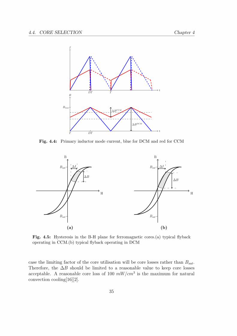
4.4. CORE SELECTION Chapter 4
I
DT Tt
B
DTTt
∆BCCM
∆BDCM
Bmax
Fig. 4.4: Primary inductor mode current, blue for DCM and red for CCM
H
B
∆I
∆B
Bsat−
Bsat−
(a)
H
B
∆I
∆B
Bsat−
Bsat−
(b)
Fig. 4.5: Hysteresis in the B-H plane for ferromagnetic cores.(a) typical flybackoperating in CCM.(b) typical flyback operating in DCM
case the limiting factor of the core utilisation will be core losses rather than Bsat.Therefore, the ∆B should be limited to a reasonable value to keep core lossesacceptable. A reasonable core loss of 100 mW/cm3 is the maximum for naturalconvection cooling[16][2].
35

4.4. CORE SELECTION Chapter 4
4.4.1 Determine the maximum flux swing (∆Bmax)
If the core is Bsat limited then the maximum B has to occur 10% above Ipeak soas to avoid any risk of saturating the core during transients or faults [16][1]. Ingeneral, the relationship between ∆I and ∆B can be expressed as
∆Bmax = Bmax∆Ipp
1.1 ∗ Ipeak(4.14)
where Bmax is the maximum allowed flux density which usually is less then Bsat
for practical reasons (in this case set to 300 mT). As can be observed from (3.3),the maximum current ripple occurs at maximum input voltage and minimum dutycycle. For our calculated value ∆Ipp of 2.93A, we get ∆Bmax=188.8 mT. Thisvalue is a peak-peak value and it should be divided by two to convert it to thepeak value. The core loss per volume due to the peak flux can be found in Fig4.3. The figure shows that when the switching frequency is 65 kHz the losses arearound 100 mW/cm3 with a peak flux of 100 mT. This means that the core of theconverter operating at 65 kHz is saturation limited and Bmax can be set to 300mT.On the contrary, when the switching frequency is 300 kHz the losses already reach100mW/cm3 when the flux density is barely 50mT. Therefore, the core for 300 kHzis loss limited and the flux swing should not be allowed to exceed 100mT(2∗50mT) if it is intended to have low losses [16].
4.4.2 Calculate windows area product AP
When the core is saturation limited, its windows area product can be estimatedby
APsat = AwAE =
(LIoverIrmsBmaxK1
) 43
(4.15)
where L is the primary inductance, Irms is the RMS value of the primary current,and K1 is a constant (K1 = 0.0085) [16]. As previously discussed, it is safe toset Bmax = 300mT and the primary inductance, the peak and the RMS currentcalculated according to (4.10), (4.11) and (4.12) respectively. The core size forthe 65 kHz converter can now be estimated to APsat = 1306mm4. To minimizethe number of iterations, it is a good idea to take a core which has a slightlybigger AP. The closest core size of the 65 kHz switching frequency transformer isEFD25.
36

4.5. DETERMING THE SECONDARY TURNS Chapter 4
When the core is loss limited, its area product can be estimated according to
APloss = AwAE =
(L∆IIrms∆BmaxK2
) 43
(4.16)
where ∆B and ∆I is the maximum flux and current swing respectively. K2 is aconstant (K2 = 0.006). The flux swing should be limited to 100mT which givesan area product of 630mm4. For the operating case with a swithching frequencyof 300kHz, an EFD20 core will be used with AP = 818mm4.
4.4.3 Determine the required number of minimum primaryturns Nmin
p
The minimum number of primary turns Nminp that can provide the desired induc-
tance value when the flux swing is maximum can be calculated as
Np =∆ImaxL
∆BmaxAe10−2 (4.17)
where L is the required inductance and Ae is the cross sectional area of the core.For the converter with the switching frequency of 65kHz, the core is saturationlimited and the value of ∆Bmax calculated from (4.14) is valid. On the otherhand, for the conveerter with the frequency of 300kHz, the core is loss limited at∆Bmax=100mT. The value of Np must be rounded to an integer value.
4.5 Determing the Secondary Turns
The output voltage reflected to the primary side of the transformer when the switchis blocking is given by
Vro =Dmax
1−Dmax
V mind . (4.18)
A simplified circuit diagram of the transformer is shown in Fig 4.6. The turns ratioof the transformer (n) can be calculated from Vro and the master output voltageVo1 which gives
37

4.5. DETERMING THE SECONDARY TURNS Chapter 4
n =Np
Ns1
=Vro
V01 + VF1
(4.19)
where VF1 is the forward voltage drop of diode D1 (1V) and Np is specified in(4.17). The number of turns for the second output is calculated from the masteroutput as
Ns2 =V02 + VF2
V01 + VF1
Ns1 (4.20)
where VF1 is the voltage drop of diode D2. Ns2 must be rounded to the nearstinteger so that the number of the primary turns does not exceed Nmin
p . The numberof turns for the auxiliary is given as
Naux =Vcc + VFauxV01 + VF1
Ns1 (4.21)
where Vcc is the nominal voltage of the control circuit and VFaux is the forwardvoltage drop of the diode Daux. The results are summarized in Table 4.4.
Np Ns1
−
+
Vro
−
+
V01
D1
Naux Ns2
−
+
Vcc
−
+
V02
D2Daux
Fig. 4.6: An ideal diagram of the transformer
Table 4.4: Number of turns and core type
Frequency [kHz] n Np Ns1 Ns2 Naux Coretype
65 1.4 14 10 5 12 EFD25
300 1.4 11 8 4 9 EFD20
38

4.6. DETERMING THE WIRE DIAMETER Chapter 4
4.6 Determing the Wire Diameter
In order to select a suitable wire size, the RMS value of the current through theprimary and the secondary side of the transformer should be known. The selectedwire should have enough cross-sectional area so that the temperature increase ofthe windings becomes sufficiently low. Table 4.5 shows the wire diameter andthe current carrying capacity of the wire with different current density. The RMSvalue of the secondary current can be calculated from the RMS value of the primarycurrent specified in (4.12) which gives
Irmssn = Irmsp NKln (4.22)
where Kl is the load occupying factor defined as
Kl =PonPo
(4.23)
where Po is the output power of the selected output. The power of the two outputsis equal and therefore Kl is the same for both outputs.
In order to utilise the cross-sectional area of the wire, a wire of diameter greaterthan twice the skin depth should be avoided. The skin depth (δ) is defined as thedistance from the surface where the current density has fallen by factor of 1/e [6].If the frequency is relatively high, the current density near the surface become veryhigh. The skin depth can be calculated as
δ =66.2√fs
[mm] (4.24)
where fs is the frequency it is subjected to. The diameter of the wires for thetransformer with the switching frequencies 65 kHz and 300 kHz should not begreater than 0.519 mm and 0.241 mm respectively. As seen from Table 4.5, wireswith Gauge # 26 and # 31 are suitable for 65 kHz and 300 kHz respectively.A suitable current density in each winding is 395A/cm2. Table 4.6 shows that anumber of parallel conductors must be used in order to reduce the skin depth whilereducing the AC-resistance. Table 4.5 summarises the results where the designfor 65kHz needs 5 parallel wires and the design for 300 kHz needs 15 parallelwires.
39

4.7. CHOOSING THE DIODES Chapter 4
Table 4.5: Copper diameter and their current carrying capacity for different A/cm2
Wire List
Gauge no Diameter[mm]
Current[A]@329A/cm2
Current[A]@395A/cm2
Current[A]@493A/cm2
25 0.455 0.534 0.6408 0.8010
26 0.404 0.4235 0.5082 0.6353
27 0.361 0.3359 0.403 0.5038
28 0.320 0.2663 0.3196 0.3995
30 0.254 0.1675 0.201 0.2513
31 0.226 0.1328 0.1594 0.1993
32 0.203 0.1053 0.1264 0.1580
Table 4.6: Rms value of the current and the required number of wires
Number of parallel wires
Current [A] RMS value 65 [kHz] 300 [kHz]
Ip 2.263 5 15
Is1 1.5864 4 10
Is2 2.978 6 19
4.7 Choosing the diodes
Proper design of the switch and the diode are essential to any switching converter.The switch has to be dimensioned to be able to withstand stresses while beingfast enough. The voltage across the diode when it is blocking is the input volt-age transferred to the secondary side of the transformed plus the output voltageaccording to
VDn = Von +Nsn
Np
V maxd (4.25)
where VDn is the voltage across the diode, Nsn is the number of secondary turnsspecified in (4.19) and (4.20) while V max
d is the maximum input voltage. Thevoltage rating of the selected diode should have at least 30% of safety margin. Thenominal voltage of the diode is 1.3VDn [18].
40

4.8. DETERMINE THE OUTPUT CAPACITORS Chapter 4
The maximum current that flows through the output diodes is the RMS current ofthe secondary which is presented in (4.6). The nominal current of the diode shouldbe at least 50% higher then the calculated value [9] to give sufficient margin. Sincethe master output is designed for 1A, a 1.5A rated diode was chosen and a 3Arated diode for the slave output (design current 2A). They were both available ata rated voltage of 90V which was beyond the requirement.
4.8 Determine the output capacitors
The output capacitors in the flyback converters provide energy to the load duringthe time that the diode is in blocking mode. See Fig 4.7(a) where the shaded areain the figure represents the charge that flows to the load and is given by
∆Q = ∆VoCo = DTIo (4.26)
where ∆Vo is the ripple in the output voltage and Co is the capacitance value. Thevalue of the ripple voltage is dependent on how sensitive the load is to voltage ripplewhich in this case is set to 0.2% of the output voltage. The minimum capacitorvalue can be now calculated as
Cmin =DIo
∆Vofs(4.27)
where fs is the switching frequency. As seen from Fig 4.7(b), the current throughthe capacitor produces a corresponding ripple voltage across the capacitor’s equiv-alent resistance (ESR). The selected capacitor must have an ESR that leads to alower ripple voltage than ∆Vo. The current rating of the capacitor is given by
Ic(rms) =√I2d − I2o (4.28)
where Id is the RMS value of the current flowing through the diode.
Table 4.7 summarises the chosen ratings of the MOSFET, the diodes and theoutput capacitors for the designed converters
41

4.9. DESIGN OF CLAMP AND DAMPING CIRCUIT Chapter 4
Ic
DT
∆Q
Tt
Io
(a)
iD
C
ic
ESR
Io
Rload
(b)
Fig. 4.7: (a)Output capacitor current.(b) Simple circuit diagram of the outputcapacitor, diode and load
Table 4.7: Ratings of the power stage components
Power ratings [V/A] Cap./ESR [µF/mΩ]
Frequency [kHz] MOSFET D1 D2 Co1 Co2
65 70/11 90/1.5 90/3 385 1539
300 70/11 90/1.5 90/3 83 333
4.9 Design of Clamp and Damping circuit
The transformer has a main flux that links the primary with the secondary andleakage flux which causes a leakage inductance. When the switch is off, the lumpedcapacitance of the switch leads to
dVDdt
=IpeakClump
. (4.29)
These spikes have a high rate of change and could exceed the breakdown valueof the MOSFET voltage therefore, a clamp circuit is needed to avoid this prob-lem.
42
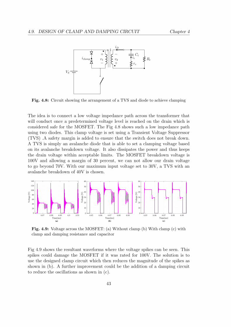
4.9. DESIGN OF CLAMP AND DAMPING CIRCUIT Chapter 4
n:1
v1−
+
v2+
−iclamp
Vd
iD
Ctic
rc
Rt
Fig. 4.8: Circuit showing the arrangement of a TVS and diode to achieve clamping
The idea is to connect a low voltage impedance path across the transformer thatwill conduct once a predetermined voltage level is reached on the drain which isconsidered safe for the MOSFET. The Fig 4.8 shows such a low impedance pathusing two diodes. This clamp voltage is set using a Transient Voltage Suppressor(TVS) .A safety margin is added to ensure that the switch does not break down.A TVS is simply an avalanche diode that is able to set a clamping voltage basedon its avalanche breakdown voltage. It also dissipates the power and thus keepsthe drain voltage within acceptable limits. The MOSFET breakdown voltage is100V and allowing a margin of 30 percent, we can not allow our drain voltageto go beyond 70V. With our maximum input voltage set to 30V, a TVS with anavalanche breakdown of 40V is chosen.
6.87 6.88 6.89 6.9 6.91
Time[ms]
0
20
40
60
80
100
120
140
Volt
age
[V]
(a)
6.85 6.86 6.87 6.88 6.89
Time[ms]
0
10
20
30
40
50
60
Volt
age
[V]
(b)
6.85 6.86 6.87 6.88 6.89
Time[ms]
0
10
20
30
40
50
60
Volt
age
[V]
(c)
Fig. 4.9: Voltage across the MOSFET: (a) Without clamp (b) With clamp (c) withclamp and damping resistance and capacitor
Fig 4.9 shows the resultant waveforms where the voltage spikes can be seen. Thisspikes could damage the MOSFET if it was rated for 100V. The solution is touse the designed clamp circuit which then reduces the magnitude of the spikes asshown in (b). A further improvement could be the addition of a damping circuitto reduce the oscillations as shown in (c).
43

4.10. COMPENSATOR DESIGN Chapter 4
4.10 Compensator Design
The first step in the compensator design procedure is to derive the transfer functionof the flyback converter. For the converter shown in Fig 4.10 the state spacecoefficients are A1 B1 C1 and D1 for the on-state in Fig 4.10(a), and A2 B2 C2 andD2 for off-mode in Fig 4.10(b)
n:1
v1−
+
v2+
−
id
rsw
isw
im
Lm
Vd
Ctic
rc
Rt
(a)
n:1
v1−
+
v2+
−
im
Lm
Vd
iD
Ctic
rc
Rt
(b)
Fig. 4.10: Equivalent circuit of a flyback converter.(a) ON mode (b) OFF mode.
The inductor current, the voltage across the ouput capacitor and the output voltagegive the states of the system. When the switch is on, the inductor current is
di
dt=Vd − imRsw
Lm, (4.30)
while the output voltage is
vo =Rt
(Rt + rc)(4.31)
and the voltage across the capacitor is
dvcdt
=vc
(Rt + rc)Ct(4.32)
where Rt and Ct are the total load resistance and capacitance respectively. For aconverter with more than one output, all the outputs appear in parallel since theinductance current is feeding all of them. Therefore, Ct and Rt are a combinationof the load resistance and capacitors of all the outputs [19]. When the switch isconducting the state equations of the system can be written as
44

4.10. COMPENSATOR DESIGN Chapter 4
vo =Rt
Rt + rcvc +
nRtrcRt + rc
im (4.33)
di
dt= − nRt
(Rt + rc)Lmvc −
n2Rtrc(Rt + rc)Lm
im (4.34)
and
dvcdt
=nRt
(Rt + rc)Cim −
1
(Rt + rc)Cvc (4.35)
The resulting state-space equations are presented in Appendix A.2. By averagingthe state space matrices, the desired transfer function of the power stage (Tp) canbe derived. The derivation of these equation are beyond the scope of this theses butstep-by-step explanation has been provided [4]. The small signal transfer functionis
Tp(s) = C[sI − A]−1[(A1 − A2)X + (B1 +B − 2)Vd] + (C1 − C2)X (4.36)
where Tp is a function of the duty cycle and the input voltage. The matlab fileprovided in Appendix A.4 simplifies (4.36) and calculates the compensation pa-rameters (C1, C2 and R2). The bode diagram of the total system is shown inFig 4.11 and shows that the system has a zero in the right hand plane when theinput voltage at its maximum. This operating point is the most critical point froma controller theory point of view and therefore the compensation parameters aredesigned at this operating point.
-50
0
50
Mag
nit
ude
(dB
)
102
103
104
105
106
107
180
270
360
Phas
e (d
eg)
Bode Diagram
Frequency (rad/s)
Fig. 4.11: Theoretical bode plot of the system
45

4.10. COMPENSATOR DESIGN Chapter 4
46
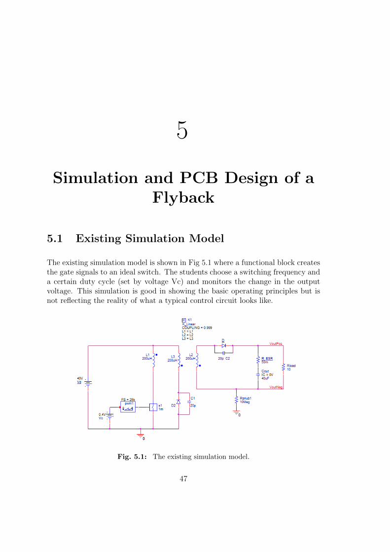
5
Simulation and PCB Design of aFlyback
5.1 Existing Simulation Model
The existing simulation model is shown in Fig 5.1 where a functional block createsthe gate signals to an ideal switch. The students choose a switching frequency anda certain duty cycle (set by voltage Vc) and monitors the change in the outputvoltage. This simulation is good in showing the basic operating principles but isnot reflecting the reality of what a typical control circuit looks like.
Fig. 5.1: The existing simulation model.
47

5.2. PROPOSED SIMULATION MODEL Chapter 5
5.2 Proposed Simulation Model
The simulation model of the flyback converter is as shown in Fig.5.2. The simu-lation was implemented using OrCAD Pspice. The manufacturer of the controllerhas provided a Spice model that was used in the simulation. A new model of thetransformer to enable multiple outputs was developed for this thesis. Below is adescription of the different signals and what effect they have on the circuit.
Fig. 5.2: Simulation model of a flyback converter with two outputs
VIN: The LM5020 works on a range of input voltages from 13V to 100V.
UVLO: Signal used to detect an under-voltage in the input and shuts down thecontroller. The designer chooses what will be the absolute minimum voltagefor the circuit to work. Using this value, a voltage divider is used to set thisvoltage to translate to the UVLO voltage minimum of 1.25V.
VCC: The output to the internal voltage regulator. This voltage is set to 7.7V.An auxiliary winding can be used to set this voltage above that to reducethe power consumption of the chip.
OUT: PWM controller output that drives the gate of the MOSFET with 1A peakcurrent capability.
48

5.3. PCB DESIGN Chapter 5
CS: Current sense pin used for cycle by cycle over-current protection. Any voltageabove 0.5V will shut off the controller. A sense resistor in series with theswitch is chosen so as to give 0.5 volts when the current threshold is reached.
SS: Soft start pin. A capacitor on this pin sets the gradual ramping of the inputto enable the output.
FB and COMP: The compensation network is connected between these two pins.
The new simulation model can be used for transient as well as steady state analysisof the circuit. The effect of having a non ideal switch, transformer, as well as diodescan then give the student a real feel of the actual converter. Students can thus usethe simulation for calculation of losses as well as design of snubber circuits for areal life flyback.
Above all, this simulation could be used to show important aspects in control of theflyback and how a proper feedback and compensation network should look like andwhat effects they have on the circuit. These control aspects can be shown throughthe step response of the output voltage. An AC analysis was not performed dueto lack of time.
5.3 PCB Design
A Printed Circuit Board (PCB) was designed for the circuit using the free programDesignSpark PCB. The PCB design process is initiated by a working simulationmodel. The simulation helps in deciding component values that will constitute thefinal circuit.
The first part of the design involves the creation of build schematics which iscomposed of how all the components are connected together. Power signals formthe main current paths through the input capacitors, the transformer and theswitch in the primary side of the converter. For the secondary side its mainlythe output diodes,capacitors and the load that have the power nodes. Since acontroller is used, it requires some signal nodes as well which are low power traces.Proper grounding is a key factor for the proper functioning of the converter as awhole while power and signal grounds have to be separated.
The following component and trace layout recommendations came in handy insetting up the final PCB board
1. When designing with a current sense resistor, all of the noise sensitive lowpower ground connections should be connected together locally to the con-
49

5.3. PCB DESIGN Chapter 5
Fig. 5.3: Top Silkscreen
troller.A single connection should be made to the high current power ground.This is recommended by the manufacturer.
2. The frequency setting resistor should be located close to the device andconnected directly to the pins of the controller
3. The decoupling capacitors on the Vin and VCC pins of the controller shouldbe located as close to the controller as possible
4. The power traces from the input voltage and in the output path should bemade as thick as possible
5. The current loops that are formed by the input source and the input capac-itors, the transformer and the switch should be made as short as possible.
6. The clamp circuit should be located as close to the transformer as possible.
7. If the load is of a resistive nature,it is likely to overheat and therefore theheat is conducted through the PCB. It is therefore recommended to placethe load on a separate PCB.
Fig 5.3 and Fig 5.4 show the top silkscreen and copper traces of the final circuit.Fig5.5 shows the bottom copper layer of the final circuit.
50

5.3. PCB DESIGN Chapter 5
Fig. 5.4: Top copper trace
Fig. 5.5: Bottom Copper
5.3.1 Current Measuring
In order to study the operation mode that a flyback converter is operating, thewaveforms of the current and the voltage should be measured The voltage and thecurrents that are important to measure is shown in Fig. 3.4, 3.3 and 3.5. There aredifferent ways that can be measured the current. One of these methods is to use acurrent sense amplifier. This device measures a voltage drop over a sense resistorplaced at the path of the current. For example, the current through the switchcan be measured by serially connecting a 100 mΩ. The current sense amplifierused in this thesis is MAX4173 which has a gain of +100V/V and wide 1.7MHzbandwidth.
51

5.3. PCB DESIGN Chapter 5
52

6
Simulations and Measurements
6.1 Simulations
The simulation model and the practical lab assignments should be connected tothe theoretical aspects of the converter as explained in chapter 3. The simulationmodel developed in this thesis is a simple model of a flyback converter in whichtransformer of the flyback is modelled as an ideal transformer in parallel with amagnetising inductance. The model is intended to demonstrate the operating prin-ciple of a flyback converter by demonstrating the different operation points (CCMand DCM) and what causes the transitions between them. Some of the parametersare summarised in (3.15) and shown in Fig. 3.6. Unlike the existing simulationmodel, this model simulates a closed loop system of a flyback converter.
6.1.1 Inductance value in CCM
The students can calculate the minimum value of the magnetising inductance Lmwhich give CCM as home assignment. The value of the magnetising inductanceused in this project is calculated from (4.10) and Fig. 6.1 shows how the wave-forms changes when the input voltage increases. This is aligned to the mathemat-ical equations demonstrated in Fig. 3.6 which show that the duty cycle decreasesas the input voltage increases. This means that the time that the transformeris discharging increases relative to the charging time and explains the transitionto DCM. Students can verify and investigate some of the mathematical relation-ship explained in chapter 3 by studying Fig. 6.1. For example, the students caninvestigate:
53

6.1. SIMULATIONS Chapter 6
11.955 11.96 11.965 11.97 11.975 11.98 11.985 11.99
Time[ms]
0
1
2
3
4
5
Cu
rren
t [A
]
Ip Is2
Is1
(a)
11.955 11.96 11.965 11.97 11.975 11.98 11.985
Time[ms]
0
1
2
3
4
5
Cu
rren
t [A
]
(b)
Fig. 6.1: Simulation: Current waveforms in a flyback converter operating in CCMmode with different input voltages: (a) Vd=15 (b) Vd=30.
• The input voltage that gives the maximum and minimum ripple currents.
• The ripple current that gives the maximum core losses. The core losses cannot be measured in the simulation but theoretically a high current rippleresults a high magnetic flux swing which in turn gives a high core losses.
• The input voltage that leads to the maximum duty cycle.
If the load is decreased, the system shifts to discontinuous conduction mode. Theduty cycle continues to decrease as the output current decreases. Fig 6.2 showsthat when the output voltage is maximum and the output current is minimum thesystem is operating in DCM. As the input voltage decreases the system shifts toCCM. This phenomena is also illustrated Fig.3.6. Load changes therefore affectthe operation mode in direct response to the energy required to be transferred tothe output. The shift between different modes can thus be achieved by changingthe load current or input voltage. The pedagogical tasks that the students caninvestigate from this are:
• When ever the input or output voltages change the resulting automaticchange in the duty cycle will be an interesting demonstration to the stu-dents.
• The system can shift to DCM if the load current decreases
6.1.2 Inductance value in DCM
The transformers magnetising inductance is a critical parameter that determinesthe operation mode. A high primary inductance Lm means that more energycan be stored in the transformer every cycle and it is very likely that this energywill not be dissipated in the same cycle, the converter will thus operate in CCM.
54

6.1. SIMULATIONS Chapter 6
6.905 6.91 6.915 6.92 6.925 6.93 6.935 6.94 6.945 6.95
Time[ms]
0
0.5
1
1.5
2
2.5
Cu
rren
t [A
]
Ip
Is2
Is1
(a)
6.91 6.915 6.92 6.925 6.93 6.935 6.94 6.945 6.95
Time[ms]
0
0.5
1
1.5
2
2.5
Cu
rren
t [A
]
(b)
Fig. 6.2: Current waveforms in a flyback converter operating in DCM mode withdifferent input voltages: (a) Vd=30 (b) Vd=15.
Lowering the inductance value will change the operation mode of the converter.This phenomena is presented in Fig. 3.6 which shows that a low inductance valueis needed in DCM. In the designed circuit, the operation point is changed byreplacing the core with another that has a bigger air gap thus decreasing theinductance value and consequently changed the operation mode. A change ofinductance from 52.5µH to 18µH for the same input and output conditions led tochange from CCM to DCM operation. The pedagogical tasks that the studentscan analyze are:
• The inductance value needed in DCM is less than one in CCM. Therefore,the size of the transformer can be reduced when operating DCM. This tasksdemonstrates that the transformer of a flyback converter is an energy storagedevice and the size of it is directly proportional to the stored energy.
• As can be observed from Fig. 6.2 and Fig. 6.3, the ripple and peak currentare relatively high in DCM compare to CCM. This leads to high losses inthe MOSFET and the diode. Therefore, it is preferred to use DCM for thelow current high voltage applications.
6.1.3 Current sense simulations
To measure the current through the switch and the diodes, a current sense amplifierwas implemented. The amplifier should have a relativity high bandwidth in orderto measure the high frequency content of the current. Fig. 6.4 shows the simulationresult where the actual value of the current is compared to the current senseresults.
55

6.1. SIMULATIONS Chapter 6
10.95 10.955 10.96 10.965 10.97 10.975 10.98 10.985 10.99 10.995 11
Time [ms]
0
1
2
3
4
5
Curr
ent
[A]
(b)
10.95 10.955 10.96 10.965 10.97 10.975 10.98 10.985 10.99 10.995 11
Time [ms]
0
1
2
3
4
5C
urr
ent
[A]
(a)
Is2
Is1Is1
IpIp
Is2
Fig. 6.3: Simulation: Current waveforms in a flyback converter operating in DCMmode with different input voltages: (a) Vd=15 (b) Vd=30.
11 11.02 11.04 11.06 11.08 11.1
Time [ms]
0
0.5
1
1.5
2
2.5
3
Cu
rren
t [A
]
Rsense
real
Fig. 6.4: Current measurement in the simulation model
6.1.4 Compensation Network
One problem for this simulation model is the compensation network which shouldbe tailored to the transfer function of the power stage. When the inductancevalue or the frequency is changed, the parameters of the compensation networkshould be recalculated which can be difficult to the students. This problem canbe solved by preparing the compensation network parameters to the students. Forexample, the Matlab file provided in Appendix A.4 calculates the compensationparameters according to the course literature in [4]. The matlab function takesthe frequency and inductance value as input arguments. And printouts the valuesof the compensation network. Fig.6.5 shows the step response of the system whena step was applied to the master output. As seen from Fig 6.5(a), the controllerreacts to bring the voltage back under control. The design of the compensationnetwork will be done for a particular operation mode which makes transitionsbetween the different operating modes particularly prone to stability issues.
On the other hand, when a step is applied on the second output (the slave output)
56

6.2. MEASUREMENTS Chapter 6
the voltage decreases as it can be observed from Fig. 6.5. An understanding ofthis concept will help the students to appreciate the role that the controller playsin stabilizing the output voltage in a flyback converter.
5 5.5 6 6.5 7 7.5 8 8.5 9
Time [ms]
4.9
4.95
5
5.05
5.1
5.15
Vo
ltag
e [V
]
(a)
9.8
9.9
10
10.1
10.2
Vo
ltag
e [V
]
9 10 11 12 13 14
Time [ms]
4.9
4.95
5
5.05
5.1
5.15
(b)
9.8
9.9
10
10.1
10.2
10.3
Vo
ltag
e [V
]
Master ouput voltage
Slave ouput voltage
Fig. 6.5: Transient responte of the output voltage: (a) When load-step is appliedat input 1 (b) When load-step applied at input 2
6.2 Measurements
One of the main aims set out in this masters thesis is to make an immediatecorrelation between the lectures and the lab exercises. The areas of study for theprototype of the circuit board are the current and voltage waveforms.
To achieve these aims, it should be possible to measure currents and voltages inthe circuit board so as to see the waveforms. The currents of interest are mainlythose through the switch and diodes. The current through the output capacitorscould also be shown. The voltages over the switch, the diode and the outputvoltage would be of interest for the objectives of the course. However, when thecurrent sense is implemented on the circuit board the result it gives is not asexpected. This could be attributed to low bandwidth as well as interference dueto non optimal placement of the current sense amplifiers. Therefore, to show theoperation of the converter, the functionality is illustrated with the voltage acrossthe switch.
Fig 6.6a shows the drain voltage for CCM operation for high output current. Thiscircuit was designed with two different load values that one can switch between.One of the loads is a high resistance load which translates to low current while theother load point is a low resistance load.
A modification was made in that the load was switched to the high resistance load
57

6.2. MEASUREMENTS Chapter 6
0.02 0.04 0.06 0.08 0.1 0.12
Time [ms]
0
10
20
30
40
50V
olt
age
[V]
(a) Drain Voltage when the load current ismaximum
0 0.01 0.02 0.03 0.04
Time [ms]
10
20
30
40
50
Vo
ltag
e [V
]
(b) Drain Voltage when the converter islightly loaded
Fig. 6.6: Measured result
thus reducing the output current. Fig 6.6b shows the resulting drain voltage. Itcan be seen that the operation point has changed to DCM.
0 0.02 0.04 0.06 0.08 0.1 0.12
Time [ms]
0
10
20
30
40
50
Volt
age
[V]
Fig. 6.7: Drain Voltage with lower inductance value
A further modification is done which involves replacing one half of the E-core withone that has a bigger gap effectively reducing the inductance value of the trans-former. Fig 6.7 shows the resulting waveforms. Not only has the operation pointgone deeper into DCM but there is evidence that the controller is not stable andsends gate signals to the MOSFET when it is in blocking mode. This as discussedearlier is one of the effects related to the compensation which was designed forCCM in this case.
58

7
Results
From pedagogical point of view, the suggested simulation model and the circuitboard upgrades the lab sessions of the flyback converter as flows:
1. One of the main aims set out in this masters thesis is to make an immediatecorrelation between the lectures and the lab exercises. This is achieved by asimple circuit as shown in Fig. 7.1. The figure shows the different parts ofthe schematic of a flyback and the corresponding parts of the circuit board.
The suggested areas of study for this circuit board are as follows:
• Load current: Change the load current by switching on two differentloads to observe the effect on the circuit waveforms.
• Inductance: Investigate the effect of changing the transformer induc-tance on the circuit waveforms. This can be achieved by changing theair gap. The advantage of this task is that it give students a practicalunderstanding how the air gap and inductance value are related.
• Compensation: Investigate the compensation network and its effect onthe stability of the output especially during transitions from CCM toDCM and vice versa. The circuit board that uses in the lab today isopen loop system and can not demonstrated the stability issue whenthe system shifts from CCM to DCM.
2. In order to investigate, the relation between frequency and the size of thetransformer, two transformers adopted for two frequencies (65 kHz and 300kHz) are designed. Fig. 7.2 shows the overview of the two transformers,the volume of the transformer with 65 kHz is 1490 mm3 and 3300 mm3 forthe transformer with 300 kHz. The size of the transformer decreases with
59

Chapter 7
control circuit
Fig. 7.1: Overview of the circuit board compered to the circuit diagram of theflyback converter.
a factor of 2 although the frequency is increases a factor of 4. This is dueto the fact that the flux swing of 65 kHz and 300 kHz are 50 mT and 100mT, respectively. A suitable pedagogical task that can demonstrate howthe frequencies affect the physical size and losses in the magnetic cores isessential. If the two converter are build the only thing that the studentscan study is the losses and compere the efficiency of the two converters.However, this is not showing much about the magnetic flux in the magneticcores. Therefore, this thesis is suggesting that the 65 kHz circuit should bebuild and use it to demonstrate practical lab assignments. Then a suitablepedagogical tasks is redesigning of the transformer, from a frequency of 65kHz to a frequency of 300 kHz. Due to the practical reasons, the students
60

Chapter 7
Fig. 7.2: Overview of two transformer with two different frequencies. The frequencyof the large and small transformers are 65 and 300 kHz respectively
can, design a transformer with frequency of 300 kHz. The important thingis that the students gets the knowledge of how to design a transformer andunderstand the basic properties such as the difference between when the coreis loss or saturation limited.
3. Demonstration of how the inductance value can change the operation modeof the converter.
• In the simulation this can be done by theoretically calculating the induc-tance value which gives CCM and it can be compared to the inductancevalue which gives DCM. The simulation model verifies if the calculatedinductor value behaves as it is supposed to. This tasks demonstratesthe function of a flyback transformer which is an energy storage de-vice. The amount of energy needed to be stored for the two operationmodes (CCM and DCM) are different, therefore their inductance valueare different.
• In the practical lab, the inductance value can be varied by changing
61

Chapter 7
the air gap. This task can give students a practical understanding howthe air gap and inductance value are related. The core used in thisproject has form of EE and has the gap between the two E. As it canbe observed from Fig. 7.2, it can be removed one of the cores andchanged to it with one which have larger or smaller gap.
4. Demonstration of how a flyback converter designed to operate in CCM canshift to DCM. This phenomena is explained and discusses in section 3.2.3.The operation mode can be changed by changing the load or the input volt-age. In the existing simulation and practical lab it can not be demonstratedwhat could happen for instance when the input voltage changes. The newsimulation model is a closed loop system and the duty cycle changes auto-matically when the input voltage changes. Therefore, the students can studyhow the duty cycle changes when the input voltage varies.
5. The flyback converter designed in this masters thesis has two outputs andthe controller regulates just one output. The reaction of the controller can beinvestigated by applying a load step. This task demonstrates that a flybackconverter my have two or more outputs but only one output can be regulated.
62

8
Discussion
The purpose of this thesis was to develop a simulation model and a circuitboard for a flyback converter to be used by students of power electronicconverters. The designed model is used to visualise the operating principle
of the flyback converter. The focus was on three main areas; different operationsmodes of the converter, transformer design and the role of the controller in theoverall function of the converter.
First the different operation modes of the converter is really at the heart of whatthe student should understand in the course. Terminology such as DCM and CCMmode of operation are a constant presence in ENM060 and ENM070. However,beyond identifying the different waveforms, it is not usually appreciated why aparticular operating mode is advantageous or what it means for the converter.Examples are when a certain operation mode is preferred over another with regardsto the output voltage and current, the stresses experienced by the switches anddiodes and sometimes why a particular operation mode is easier to stabilize thanthe other.
Secondly,for the flyback converter, the transformer plays an important role as anenergy storage element. Even though the design of a truly optimised transformermay be a daunting task with many considerations, a general feel for how to makedesign choices may be a desirable outcome of future lab work. Principles suchas the effect that the switching frequency has on the size of the transformer, therole of the air-gap, and the saturation effects are of importance to the student.Two different transformers were designed for 65kHz and 300kHz and the resultsshow that it is not really a scaling factor that is applicable for the two differentfrequencies. The inductance value will grow proportionally but the this is nottrue for the physical size as well. The magnetic flux swing allowed for 65kHz
63
Chapter 8
is double that for 300kHz (in the range of 200mT) which leads to different coreutilization.
Finally, the controller ensures proper functionality of the converter but is oftensidelined in the current course material and its function replaced by PWM gener-ation blocks. It has become clear that a thorough understanding of the controlleris essential for the student. Although it may not be necessarily detailed knowl-edge that is the aim here, at the very least an understanding of how to choosethe right controller is beneficial. Feedback design and compensation is key toproper functioning of the converter. Other functions of the controller such as over-current protection and undervoltage lockout (UVLO) could be introduced to thestudents.
To verify that it is possible to introduce the student to the concepts discussedabove, two tasks were undertaken as initial work towards improving the existinglab. A simulation model based on an actual controller and a model of the trans-former was built. A PCB prototype was also designed and built and measurementsmade to verify that it is possible to show the concepts to the students. It is pro-posed that building the circuit to have as few components as possible and having alayout that is close to what the students are used to seeing in schematics will be ofimmense benefit to the learning process. However, the current sense amplifier didnot work as it suppose to. Measuring of the current through the switch and thediodes are very important and students should be able to measure it. The currentsense amplifier is simulated before it was implemented and the result shows thatthe amplifier has enough bandwidth to measure the current. However, in the prac-tical lab the result that the current sense amplifier gives is not correct. This can bedue to one or several reasons combined together. The current sense is placed nearthe transformer and there is a chance that the leakage inductance can cause a highdi/dt which can effect the performance of the current sense. Another problem isthat the current sense is not placed close enough to the sense resistor which makesthe system vulnerable to the disturbances from the other devices. However, theexact reason that the current sense did not work was investigated due to the lackof time.
64
9
Conclusion and Future Work
9.1 Conclusion
Power electronics is an important area that has numerous applications and israpidly expanding. A good base knowledge is essential for students in the mastersprogram in Electric Power Engineering. This thesis has investigated the existinglab and suggested areas where it could be necessary to put a bit more focus byenhancing subjects taught in the lectures with practical lab work. It is clearthat emphasis should be placed on the different operation modes; when and whythey are applicable and what design choices have to be made to attain such aconverter.
A simulation model for a two output converter was created and a prototype PCBboard built based on this. The designed simulation and prototype board has fewcomponents which makes it possible for their use as supplementary materials inthe courses. Three main areas came out as focus points for this thesis; a thouroghunderstanding of modes of operations, magnetics design and controller design.These three areas should form a good basis for lab work in these courses.
A major suggestion of this work is that a design project should be created tosimulate and build a DC/DC converter. To fit within the allocated time, thestudents should have a ready PCB board but they should then focus on choosingthe right components and designing a flyback transformer.
65

9.2. FUTURE WORK Chapter 9
9.2 Future Work
There are a few areas that require further work and analysis. Below are some fewof the most important.
• Isolation: The designed feedback loop is a non isolated. However, it is quitecommon that modern flyback converters are isolated using an opto couplernetwork. This would form an excellent task in improving our flyback design.
• Current Measurement: A current sense amplifier was used to try and visu-alize the current through the switch and diodes. However the results werenot as expected. This was attributed to the bandwidth of the amplifier ICwhich was probably not sufficient. Different amplifier components were seento give better results in the simulations which should be invistigated further.
• Load: The load was made of power resistors which got quite hot if theconverter was operated for longer periods. Further work in this area couldbe suggestion of different types of loads or even designing of heat sinks.
• Compensation: As discussed in the results, instability was observed in themeasurements during transition from CCM to DCM. Further analysis on thecompensation network for the flyback converter is therefore necessary.
• PCB Design: There are various improvements that could be made on thecompactness as well as other aspects of the PCB.
66

Bibliography
[1] FairChild Semiconductor, Design Guidelines for Off-line flyback converter Us-ing Fairchild Power Siwtch (FPS), rev.1.0.3 (1 2003).
[2] A. I. Pressman, K. H. Billings, T. Morey, A. (e-book collection), Switchingpower supply design, 3rd Edition, McGraw-Hill, New York, 2009.
[3] M. Brown, S. A. (e-book collection), S. (e-book collection), Practical switchingpower supply design, Academic Press, San Diego, 1990;2012;.
[4] N. Mohan, T. M. Undeland, W. P. Robbins, Power electronics: converters,applications and design, 3rd Edition, Wiley, Hoboken, N.J, 2003.
[5] M. K. Kazimierczuk, Pulse-width modulated DC-DC power converters, Wiley,Chichester, U.K, 2008.
[6] S. Maniktala, S. (e-book collection), B. (e-book collection), Switchingpower supplies A to Z, second;2nd;2; Edition, Elsevier/Newnes, Amsterdam,2012;2014;.
[7] S. Maniktala, S. (e-book collection), B. (e-book collection), K. (e-book col-lection), E. (e-book collection), I. Books24x7, Troubleshooting switchingpower converters: a hands-on guide, Elsevier/Newnes, Amsterdam;Boston;,2008;2011;2007;2014;.
[8] N. Coruh, S. Urgun, T. Erfidan, Design and implementation of flyback con-verters, 2010, pp. 1189–1193.
[9] Infineon Technologies North America, Design Guide for Off-line Fixed Fre-quency DCM Flyback Converter, design Note DN 2013-01 (1 2013).
[10] C. W. T. McLyman, Transformer and inductor design handbook, 3rd Edition,Vol. 121., Dekker, New York, 2004.
67
BIBLIOGRAPHY
[11] D. K. Cheng, Field and wave electromagnetics, 2nd Edition, Addison-WesleyPub. Co, Reading, Mass, 1989.
[12] R. W. Erickson, D. Maksimovic, S. A. (e-book collection), Fundamentals ofPower Electronics, 2nd Edition, Springer, New York, 2012.
[13] W. G. Hurley, W. H. Wolfle, B. (e-book collection), E. (e-book collection),I. Books24x7, Transformers and inductors for power electronics: theory, designand applications, 1st Edition, Wiley-Blackwell, Chichester, West Sussex, 2013.
[14] STMicroelectronics, OFFLINE FLYBACK CONVERTERS DESIGNMETHODOLOGY WITH THE L6590 FAMILY, rev.1 (5 2001).
[15] C. P. Basso, A. (e-book collection), Switch-mode power supplies: SPICE sim-ulations and practical designs, McGraw-Hill, New York, 2008.
[16] Texas Instruments Incorporated, Inductor and flyback Transformer Design,section 5 (5 2001).
[17] Texas Instruments Incorporated, Power Transformer Design, section 4 (12011).
[18] D. Z. Chen, B. D. Bai, Multiple output single-ended flyback dc-dc switchingpower supply design, Applied Mechanics and Materials 392 (2013) 494.
[19] H. Choi, Practical feedback loop design considerations for switched modepower supplies.
68

A
Derivations of the mathematicalequations
A.1 Converter
The RMS value of the current is defined as:
Irms =
√1
T
∫ T
0
i(t)2dt (A.1)
The definition for Simpsons rule is:
1
T
∫ to+T
to
f(x)dx =1
6(f(to) + 4f(to +
T
2) + f(to + T ) (A.2)
The RMS current of the primary inductance operating in CCM can be calculatedas:
A1

A.2. CONTROL Chapter A
Irms =
√D
1
DT
∫ DT
0
imdt
=
√√√√D
6
[(Im − (
∆im2
)2
) + (4Im)2 +
(Im + (
∆im2
)
)2]
=
√√√√D
6
[6I2m + 2
(∆im
2)
)2]
=
√√√√D
3
[3I2m +
(∆im
2)
)2]
(A.3)
A.2 Control
On-mode state-space
A1 =
(rswLm
0
0 1(Rt+rc)
)B1 =
(1Lm
0
)C1 =
(0 Rt
Rt+rc
)
A2 =
n2RtrcLm(Rt+rc)
−nRt
Lm(Rt+rc)
nRt
Ct(Rt+rc)−1
(Rt+rc)
, B2 =
(0
0
)C2 =
(nRtrcRt+rc
Rt
Rt+rc
)and state average isA=A1D + A2(1-D)B=B1D + B2(1-D)C=C1D + C2(1-D)
where D is duty cycle
A.3 Filter
A.4 Matlab code for compensation network
A2

A.4. MATLAB CODE FOR COMPENSATION NETWORK Chapter A
f unc t i on [ R1 , C1 , C2 ] = compen ( fsw ,Lm)
s = t f ( ’ s ’ ) ;
% ∗∗∗∗∗∗∗∗∗∗∗∗∗∗∗∗∗∗∗∗∗∗∗∗∗∗∗∗∗∗∗∗∗% Component cons tant s% ∗∗∗∗∗∗∗∗∗∗∗∗∗∗∗∗∗∗∗∗∗∗∗∗∗∗∗∗∗∗∗∗∗
Vo1=10;Io1 =1;
Vo2=5;Io2 =2;
Rl1 =10;Rl2 =2.5;% the output load i s the t o t a l loadRload=(Rl1∗Rl2 )/ ( Rl1+Rl2 ) ;
% Input vo l tage , turn r a t i o and swi t ch ing fequancyVd=30;Dmin=0.333;Dmax=0.5;f s=fsw ∗1 e3 ;n1 =1.4;RT1=(1/( f s ∗158e−12))∗1e−3;
% Magnetis ing inductance ;Lm=Lm∗1e−6;
% Ca l cu la t i on o f Output c a p c i t o r s
Voutrps =0.002∗10; % r i p p l e vo l tage houtput 1Voutrpt =0.002∗5;% r i p p l e vo l tage output 2
Co1=(( Io1 ∗Dmax)/( f s ∗Voutrps ) ) ;
A3

A.4. MATLAB CODE FOR COMPENSATION NETWORK Chapter A
Co2=(( Io2 ∗Dmax)/( f s ∗Voutrpt ) ) ;
Cout=(Co1+Co2 ) ; % the t o t a l cap . i s Cout1//Cout2rc=30e−3; % ESRrsw=70e−3; %DCR
% Peak value o f sawtooth waveVtr i = 10 ;
%∗∗∗∗∗∗∗∗∗∗∗∗∗∗∗∗∗∗∗∗∗∗∗∗∗∗∗∗∗∗∗∗∗∗∗∗∗∗∗∗∗∗∗∗∗∗∗∗% State s o f the power s tage : x’=Ax+Bu ; y=Cx+Du ∗∗%∗∗∗∗∗∗∗∗∗∗∗∗∗∗∗∗∗∗∗∗∗∗∗∗∗∗∗∗∗∗∗∗∗∗∗∗∗∗∗∗∗∗∗∗∗∗∗∗∗
a211=(n1ˆ2∗Rload∗ rc )/ (Lm∗( Rload+rc ) ) ;a212=(n1∗Rload )/ (Lm∗( Rload+rc ) ) ;a221=(n1∗Rload )/ ( Cout∗( Rload+rc ) ) ;a222 =1/(( Rload+rc )∗Cout ) ;
A1=[−rsw/Lm, 0 ; 0 , 1/( ( Rload+rc )∗Cout ) ] ;
A2=[−a211 ,−a212 ; a221 ,−a222 ] ;
B1=[1/Lm; 0 ] ;B2 = [ 0 ; 0 ] ;
C11=[0 , Rload /( Rload+rc ) ] ;C22=[( Rload∗ rc ∗n1 )/ ( Rload+rc ) , Rload /( Rload+rc ) ] ;
A=A1∗Dmin+A2∗(1−Dmin ) ;B=B1∗Dmin ;C=C11∗Dmin+C22∗(1−Dmin ) ;X=inv (A)∗−B∗Vd;f =((A1−A2)∗X+(B1−B2)∗Vd ) ;
%∗∗∗∗∗∗∗∗∗∗∗∗∗∗∗∗∗∗∗∗∗∗∗∗∗∗∗∗∗∗∗∗∗∗∗∗∗∗%% Trans fe r func t i on o f power s tage %%%∗∗∗∗∗∗∗∗∗∗∗∗∗∗∗∗∗∗∗∗∗∗∗∗∗∗∗∗∗∗∗∗∗∗∗∗∗
A4

A.4. MATLAB CODE FOR COMPENSATION NETWORK Chapter A
Tp=s i m p l i f y (C∗ inv ( s∗ eye (2)−A)∗ f +(C11−C22)∗X) ;%bode (Tp ) :[ z , p , k ] = zpkdata (Tp, ’ v ’ ) ;wz1=abs ( r e a l (min ( z ( 2 ) ) ) ) ;wz2=abs ( r e a l (max( z ) ) ) ;wp1=abs ( r e a l (min (p ) ) ) ;
Tm = 1/ Vtr i ;%% From matlab f i l e used in the ENM060 course wr i t t en%%by Massimo Bongiorno and Andreas Karvonen , November 2007% Add the modulator and the power−s tage toghether
T converter = Tp∗Tm;% %∗∗∗∗∗∗∗∗∗∗∗∗∗∗∗∗∗∗∗∗∗∗∗∗∗∗∗∗∗∗∗∗∗% % Design o f r e g u l a t o r% % ∗∗∗∗∗∗∗∗∗∗∗∗∗∗∗∗∗∗∗∗∗∗∗∗∗∗∗∗∗∗∗∗∗%% % Desired c r o s s o v e r f requency% % Should be at l e a s t a tenth o f the sw i tch ing f requency
wcross = 0.06∗ f s ∗2∗ pi ; %To be changed during the l a b o r a t i o n !
% % Des ired phase margin and conver s i on to rad iansphase margin = 55 ;PM = phase margin∗ pi /180 ;
% Phase o f t r a n s f e r func t i on T1 at c r o s s o v e r f requency% See f i g u r e 10−25.f i 1 = phase ( f r e q r e s p ( T converter , wcross ) )
% Calcu la te the needed phase−boost at the cros s−over f requency% See equat ion 10−112boost = PM − f i 1 − pi /2 ;
% Calcu la te the f a c t o r K.% See equat ion 10−108K = tan ( p i /4 + boost / 2 ) ;G=1/abs ( f r e q r e s p ( T converter , wcross ) ) ;% Determine the component cons tant s with he lp o f the f a c t o r K.
A5

A.4. MATLAB CODE FOR COMPENSATION NETWORK Chapter A
% See equat ions 10−115 , 10−115 and 10−117.R1 = 2.43 e3 ;C2 = abs ( f r e q r e s p ( T converter , wcross ) ) / (K∗wcross∗R1 ) ;C1 = C2∗(Kˆ2 − 1 ) ;R2 = K/(C1∗wcross ) ;
% I n t e g r a t o r gain% See equat ion 10−102A = 1/(R1∗C2 ) ;
% C o n t r o l l e r ze ro% See equat ion 10−104wz = 1/(R2∗C1 ) ; %−4.04e3 ;
% C o n t r o l l e r po l e% See equat ion 10−105wp = (C1 + C2)/(R2∗C1∗C2);% −4.1860 e5 ;
% Trans fe r func t i on f o r c o n t r o l l e r% See equat ion 10−103T c o n t r o l l e r = A∗ ( ( s + wz )/( s ∗( s + wp ) ) ) ;
%end%
% % Inc lud ing c o n t r o l l e r , PWM−modulator and power s tage .T open loop = T c o n t r o l l e r ∗T converter ;
T c lo s ed loop = feedback ( T open loop , 1 ) ;
% Make a step in the c o n t r o l vo l tage at t =0.8ms[Y, X] = step ( T c losed loop , 2 e−3);
f i g u r e ;p l o t (X∗1e3 , Y, ’b ’ , ’ LineWidth ’ , 2 ) ;%a x i s ( [ 0 0 . 5 4 .8 6 . 5 ] ) ;x l a b e l ( ’ time [ ms ] ’ ) ;y l a b e l ( ’ Output Voltage ’ ) ;g r i d on
%%
A6

A.4. MATLAB CODE FOR COMPENSATION NETWORK Chapter A
di sp ( ’ Design Parmeters o f Compensation Network ’ )
formatSpec = ( ’\ nGain : %.0 f dB.\ nZero : %.0 f rad/ s .\ nPole . . .: %.0 f rad/ s .\nR2 : %2.4 f kOhm.\nC1 : %2.4 fnF\nC2. . .: %2.4 fnF\nRT1 : %2.4 f kohm.\n\n ’ ) ;f p r i n t f ( formatSpec ,A, wz , wp, R2∗1e−3,C2∗1e9 , C1∗1e9 ,RT1)
formatSpec = ( ’ Output1 Cap . : %.0 f uF .\ nOutput2 Cap .. . .: %2.4 f uF .\n\n ’ ) ;f p r i n t f ( formatSpec , Co1∗1e6 , Co2∗1 e6 )
A7

A.4. MATLAB CODE FOR COMPENSATION NETWORK Chapter A
A8

B
Data sheets
B.1 N87 datasheet
A1

Data SheetData SheetDate: September 2006
© EPCOS AG 2006. Reproduction, publication and dissemination of this publication, enclosures hereto and the information contained therein without EPCOS’ prior express consent is prohibited.
Ferrites and accessories
SIFERRIT material N87

2 09/06Please read Cautions and warnings and Important notes at the end of this document.
Material properties
Preferred application Power transformers
Material N87
Base material MnZn
Symbol Unit
Initial permeability (T = 25 °C)
i 2200 25%
Flux density (H = 1200 A/m, f = 10 kHz)
BS (25 °C) BS (100 °C)
mT mT
490 390
Coercive field strength (f = 10 kHz)
Hc (25 °C) Hc (100 °C)
A/m 21 13
Optimum frequency range kHz 25 … 500
Hysteresis material constant
B 10–6/mT <1.0
Curie temperature TC °C >210
Mean value of F at 25 … 55 °C
10–6/K 4
Density (typical values) kg/m3 4850
Relative core losses (typical values)
PV
25 kHz, 200 mT, 100 °C kW/m3 57
100 kHz, 200 mT, 100 °C kW/m3 375
300 kHz, 100 mT, 100 °C kW/m3 390
500 kHz, 50 mT, 100 °C kW/m3 215
Resistivity m 10
Core shapes RM, P, PM, ETD, EFD, E, ER, EP, EQ, ELP, U, Toroid
N87SIFERRIT materials

3 09/06Please read Cautions and warnings and Important notes at the end of this document.
N87 SIFERRIT materials
Complex permeability versus frequency (measured on R34 toroids, B 0.25 mT)
FAL0596-E
110
210
310
410
f
100
10
’ ;sµ ’’µs
102_ _1 100 101 210MHz
’sµ
’’sµ
Amplitude permeability versus AC field flux density (measured on R34 toroids, B 0.25 mT)
FAL0598-V
00
B
aµ
100 200 300 400 mT 500
< 10 kHzf25 ˚C
1000
2000
3000
4000
6000
100 ˚C
Initial permeability i
versus temperature (measured on R34 toroids, B 0.25 mT)
FAL0597-M
T
µi
˚C
1000
2000
3000
5000
20 60 100 140 180 2600_60 20_

4 09/06Please read Cautions and warnings and Important notes at the end of this document.
N87SIFERRIT materials
Dynamic magnetization curves (typical values) (f = 10 kHz, T = 25 °C)
FAL0599-4
H
0
B
-200 0 200 400 600 800 1000 A/m 1400
mT
100
200
300
500
DC magnetic bias of P, RM, PM and E cores (B 0.25 mT, f = 10 kHz, T = 25 °C)
FAL0601-J
µrev
10100
5
5
5
5
101
102
104
100 101 102 104
µe = 1000
1_
500
200
100
50
A/mDCH
Dynamic magnetization curves (typical values) (f = 10 kHz, T = 100 °C)
FAL0600-B
H
0
B
-200 0 200 400 600 800 1000 A/m 1400
100
200
300
400
500
mT
DC magnetic bias of P, RM, PM and E cores (B 0.25 mT, f = 10 kHz, T = 100 °C)
FAL0602-S
µrev
10100
5
5
5
5
101
102
104
100 101 102 104
µe = 1000
1_
500
200
100
50
A/mDCH

5 09/06Please read Cautions and warnings and Important notes at the end of this document.
N87SIFERRIT materials
Relative core losses versus AC field flux density (measured on R34 toroids)
VPmkW
3
= 100 kHzf
100 ˚C
B
25 ˚C
FAL0603-1
010
110
210
310
110 210 310mT
Relative core losses versus frequency (measured on R34 toroids)
FAL0605-H
PV
kW
10
f
m 3
010
110
210
310
410
101 5 kHz
100 ˚C1_
102 310
25 ˚C
200 mT
100 mT
50 mT
25 mT
Relative core losses versus temperature (measured on R34 toroids)
FAL0604-9
f
5
1
20
5
5
10
210
310
410
kW/m
T
PV
40 60 80 100 ˚C 120
3 = 100 kHz
200 mT
100 mT
50 mT
100
25 mT

6 09/06
SIFERRIT materialsCautions and warnings
General
Based on IEC 60401-3, the data specified here are typical data for the material in question, which have been determined principally on the basis of toroids (ring cores).
The purpose of such characteristic material data is to provide the user with improved means for comparing different materials.
There is no direct relationship between characteristic material data and the data measured using other core shapes and/or core sizes made of the same material. In the absence of further agree-ments with the manufacturer, only those specifications given for the core shape and/or core size in question are binding.
Effects of core combination on AL value
Stresses in the core affect not only the mechanical but also the magnetic properties. It is apparent that the initial permeability is dependent on the stress state of the core. The higher the stresses are in the core, the lower is the value for the initial permeability. Thus the embedding medium should have the greatest possible elasticity.
For detailed information see Data Book 2007, chapter “General – Definitions, 8.2”.
Heating up
Ferrites can run hot during operation at higher flux densities and higher frequencies.

7 04/09
Important notes
The following applies to all products named in this publication:
1. Some parts of this publication contain statements about the suitability of our products forcertain areas of application. These statements are based on our knowledge of typicalrequirements that are often placed on our products in the areas of application concerned. Wenevertheless expressly point out that such statements cannot be regarded as bindingstatements about the suitability of our products for a particular customer application.
As a rule, EPCOS is either unfamiliar with individual customer applications or less familiar withthem than the customers themselves. For these reasons, it is always ultimately incumbent on thecustomer to check and decide whether an EPCOS product with the properties described in theproduct specification is suitable for use in a particular customer application.
2. We also point out that in individual cases, a malfunction of electronic components or failurebefore the end of their usual service life cannot be completely ruled out in the current stateof the art, even if they are operated as specified. In customer applications requiring a veryhigh level of operational safety and especially in customer applications in which the malfunctionor failure of an electronic component could endanger human life or health (e.g. in accidentprevention or life-saving systems), it must therefore be ensured by means of suitable design ofthe customer application or other action taken by the customer (e.g. installation of protectivecircuitry or redundancy) that no injury or damage is sustained by third parties in the event ofmalfunction or failure of an electronic component.
3. The warnings, cautions and product-specific notes must be observed.
4. In order to satisfy certain technical requirements, some of the products described in thispublication may contain substances subject to restrictions in certain jurisdictions (e.g.because they are classed as hazardous). Useful information on this will be found in ourMaterial Data Sheets on the Internet (www.epcos.com/material). Should you have any moredetailed questions, please contact our sales offices.
5. We constantly strive to improve our products. Consequently, the products described in thispublication may change from time to time. The same is true of the corresponding productspecifications. Please check therefore to what extent product descriptions and specificationscontained in this publication are still applicable before or when you place an order.
We also reserve the right to discontinue production and delivery of products.Consequently, we cannot guarantee that all products named in this publication will always beavailable.
The aforementioned does not apply in the case of individual agreements deviating from theforegoing for customer-specific products.
6. Unless otherwise agreed in individual contracts, all orders are subject to the current versionof the “General Terms of Delivery for Products and Services in the Electrical Industry”published by the German Electrical and Electronics Industry Association (ZVEI).
7. The trade names EPCOS, BAOKE, Alu-X, CeraDiode, CSMP, CSSP, CTVS, DSSP, MiniBlue,MKK, MLSC, MotorCap, PCC, PhaseCap, PhaseCube, PhaseMod, SIFERRIT, SIFI, SIKOREL,SilverCap, SIMDAD, SIMID, SineFormer, SIOV, SIP5D, SIP5K, ThermoFuse, WindCap aretrademarks registered or pending in Europe and in other countries. Further information will befound on the Internet at www.epcos.com/trademarks.


![1 INTRODUCTION T IJSER€¦ · multioutput dc–dc converters [13]. In [14] and [15], nonisolated multiinput multioutput converter has large number of switch-es which cause low efficiency](https://img.dokumen.tips/doc/110x75/5f0b60887e708231d43037e7/1-introduction-t-ijser-multioutput-dcadc-converters-13-in-14-and-15-nonisolated.jpg)